EP4125122A1 - Method of assembling semiconductor devices and corresponding semiconductor device - Google Patents
Method of assembling semiconductor devices and corresponding semiconductor device Download PDFInfo
- Publication number
- EP4125122A1 EP4125122A1 EP22187591.7A EP22187591A EP4125122A1 EP 4125122 A1 EP4125122 A1 EP 4125122A1 EP 22187591 A EP22187591 A EP 22187591A EP 4125122 A1 EP4125122 A1 EP 4125122A1
- Authority
- EP
- European Patent Office
- Prior art keywords
- electrically conductive
- semiconductor die
- die
- semiconductor
- ribbons
- Prior art date
- Legal status (The legal status is an assumption and is not a legal conclusion. Google has not performed a legal analysis and makes no representation as to the accuracy of the status listed.)
- Pending
Links
Images



Classifications
-
- H—ELECTRICITY
- H10—SEMICONDUCTOR DEVICES; ELECTRIC SOLID-STATE DEVICES NOT OTHERWISE PROVIDED FOR
- H10W—GENERIC PACKAGES, INTERCONNECTIONS, CONNECTORS OR OTHER CONSTRUCTIONAL DETAILS OF DEVICES COVERED BY CLASS H10
- H10W70/00—Package substrates; Interposers; Redistribution layers [RDL]
- H10W70/40—Leadframes
- H10W70/464—Additional interconnections in combination with leadframes
- H10W70/466—Tape carriers or flat leads
-
- H—ELECTRICITY
- H10—SEMICONDUCTOR DEVICES; ELECTRIC SOLID-STATE DEVICES NOT OTHERWISE PROVIDED FOR
- H10W—GENERIC PACKAGES, INTERCONNECTIONS, CONNECTORS OR OTHER CONSTRUCTIONAL DETAILS OF DEVICES COVERED BY CLASS H10
- H10W70/00—Package substrates; Interposers; Redistribution layers [RDL]
- H10W70/40—Leadframes
- H10W70/479—Leadframes on or in insulating or insulated package substrates, interposers, or redistribution layers
-
- H—ELECTRICITY
- H10—SEMICONDUCTOR DEVICES; ELECTRIC SOLID-STATE DEVICES NOT OTHERWISE PROVIDED FOR
- H10W—GENERIC PACKAGES, INTERCONNECTIONS, CONNECTORS OR OTHER CONSTRUCTIONAL DETAILS OF DEVICES COVERED BY CLASS H10
- H10W70/00—Package substrates; Interposers; Redistribution layers [RDL]
- H10W70/40—Leadframes
- H10W70/481—Leadframes for devices being provided for in groups H10D8/00 - H10D48/00
-
- H—ELECTRICITY
- H10—SEMICONDUCTOR DEVICES; ELECTRIC SOLID-STATE DEVICES NOT OTHERWISE PROVIDED FOR
- H10W—GENERIC PACKAGES, INTERCONNECTIONS, CONNECTORS OR OTHER CONSTRUCTIONAL DETAILS OF DEVICES COVERED BY CLASS H10
- H10W90/00—Package configurations
-
- H—ELECTRICITY
- H10—SEMICONDUCTOR DEVICES; ELECTRIC SOLID-STATE DEVICES NOT OTHERWISE PROVIDED FOR
- H10W—GENERIC PACKAGES, INTERCONNECTIONS, CONNECTORS OR OTHER CONSTRUCTIONAL DETAILS OF DEVICES COVERED BY CLASS H10
- H10W90/00—Package configurations
- H10W90/811—Multiple chips on leadframes
-
- H—ELECTRICITY
- H10—SEMICONDUCTOR DEVICES; ELECTRIC SOLID-STATE DEVICES NOT OTHERWISE PROVIDED FOR
- H10W—GENERIC PACKAGES, INTERCONNECTIONS, CONNECTORS OR OTHER CONSTRUCTIONAL DETAILS OF DEVICES COVERED BY CLASS H10
- H10W72/00—Interconnections or connectors in packages
- H10W72/071—Connecting or disconnecting
- H10W72/073—Connecting or disconnecting of die-attach connectors
-
- H—ELECTRICITY
- H10—SEMICONDUCTOR DEVICES; ELECTRIC SOLID-STATE DEVICES NOT OTHERWISE PROVIDED FOR
- H10W—GENERIC PACKAGES, INTERCONNECTIONS, CONNECTORS OR OTHER CONSTRUCTIONAL DETAILS OF DEVICES COVERED BY CLASS H10
- H10W72/00—Interconnections or connectors in packages
- H10W72/071—Connecting or disconnecting
- H10W72/073—Connecting or disconnecting of die-attach connectors
- H10W72/07331—Connecting techniques
- H10W72/07337—Connecting techniques using a polymer adhesive, e.g. an adhesive based on silicone or epoxy
-
- H—ELECTRICITY
- H10—SEMICONDUCTOR DEVICES; ELECTRIC SOLID-STATE DEVICES NOT OTHERWISE PROVIDED FOR
- H10W—GENERIC PACKAGES, INTERCONNECTIONS, CONNECTORS OR OTHER CONSTRUCTIONAL DETAILS OF DEVICES COVERED BY CLASS H10
- H10W72/00—Interconnections or connectors in packages
- H10W72/071—Connecting or disconnecting
- H10W72/075—Connecting or disconnecting of bond wires
-
- H—ELECTRICITY
- H10—SEMICONDUCTOR DEVICES; ELECTRIC SOLID-STATE DEVICES NOT OTHERWISE PROVIDED FOR
- H10W—GENERIC PACKAGES, INTERCONNECTIONS, CONNECTORS OR OTHER CONSTRUCTIONAL DETAILS OF DEVICES COVERED BY CLASS H10
- H10W72/00—Interconnections or connectors in packages
- H10W72/071—Connecting or disconnecting
- H10W72/075—Connecting or disconnecting of bond wires
- H10W72/07551—Connecting or disconnecting of bond wires characterised by changes in properties of the bond wires during the connecting
- H10W72/07552—Connecting or disconnecting of bond wires characterised by changes in properties of the bond wires during the connecting changes in structures or sizes
-
- H—ELECTRICITY
- H10—SEMICONDUCTOR DEVICES; ELECTRIC SOLID-STATE DEVICES NOT OTHERWISE PROVIDED FOR
- H10W—GENERIC PACKAGES, INTERCONNECTIONS, CONNECTORS OR OTHER CONSTRUCTIONAL DETAILS OF DEVICES COVERED BY CLASS H10
- H10W72/00—Interconnections or connectors in packages
- H10W72/071—Connecting or disconnecting
- H10W72/076—Connecting or disconnecting of strap connectors
- H10W72/07631—Techniques
- H10W72/07632—Compression bonding, e.g. thermocompression bonding
- H10W72/07633—Ultrasonic bonding, e.g. thermosonic bonding
-
- H—ELECTRICITY
- H10—SEMICONDUCTOR DEVICES; ELECTRIC SOLID-STATE DEVICES NOT OTHERWISE PROVIDED FOR
- H10W—GENERIC PACKAGES, INTERCONNECTIONS, CONNECTORS OR OTHER CONSTRUCTIONAL DETAILS OF DEVICES COVERED BY CLASS H10
- H10W72/00—Interconnections or connectors in packages
- H10W72/50—Bond wires
- H10W72/521—Structures or relative sizes of bond wires
- H10W72/527—Multiple bond wires having different sizes
-
- H—ELECTRICITY
- H10—SEMICONDUCTOR DEVICES; ELECTRIC SOLID-STATE DEVICES NOT OTHERWISE PROVIDED FOR
- H10W—GENERIC PACKAGES, INTERCONNECTIONS, CONNECTORS OR OTHER CONSTRUCTIONAL DETAILS OF DEVICES COVERED BY CLASS H10
- H10W72/00—Interconnections or connectors in packages
- H10W72/50—Bond wires
- H10W72/541—Dispositions of bond wires
- H10W72/5445—Dispositions of bond wires being orthogonal to a side surface of the chip, e.g. parallel arrangements
-
- H—ELECTRICITY
- H10—SEMICONDUCTOR DEVICES; ELECTRIC SOLID-STATE DEVICES NOT OTHERWISE PROVIDED FOR
- H10W—GENERIC PACKAGES, INTERCONNECTIONS, CONNECTORS OR OTHER CONSTRUCTIONAL DETAILS OF DEVICES COVERED BY CLASS H10
- H10W72/00—Interconnections or connectors in packages
- H10W72/50—Bond wires
- H10W72/541—Dispositions of bond wires
- H10W72/5449—Dispositions of bond wires not being orthogonal to a side surface of the chip, e.g. fan-out arrangements
-
- H—ELECTRICITY
- H10—SEMICONDUCTOR DEVICES; ELECTRIC SOLID-STATE DEVICES NOT OTHERWISE PROVIDED FOR
- H10W—GENERIC PACKAGES, INTERCONNECTIONS, CONNECTORS OR OTHER CONSTRUCTIONAL DETAILS OF DEVICES COVERED BY CLASS H10
- H10W72/00—Interconnections or connectors in packages
- H10W72/50—Bond wires
- H10W72/59—Bond pads specially adapted therefor
-
- H—ELECTRICITY
- H10—SEMICONDUCTOR DEVICES; ELECTRIC SOLID-STATE DEVICES NOT OTHERWISE PROVIDED FOR
- H10W—GENERIC PACKAGES, INTERCONNECTIONS, CONNECTORS OR OTHER CONSTRUCTIONAL DETAILS OF DEVICES COVERED BY CLASS H10
- H10W72/00—Interconnections or connectors in packages
- H10W72/60—Strap connectors, e.g. thick copper clips for grounding of power devices
- H10W72/641—Dispositions of strap connectors
- H10W72/647—Dispositions of multiple strap connectors
-
- H—ELECTRICITY
- H10—SEMICONDUCTOR DEVICES; ELECTRIC SOLID-STATE DEVICES NOT OTHERWISE PROVIDED FOR
- H10W—GENERIC PACKAGES, INTERCONNECTIONS, CONNECTORS OR OTHER CONSTRUCTIONAL DETAILS OF DEVICES COVERED BY CLASS H10
- H10W72/00—Interconnections or connectors in packages
- H10W72/60—Strap connectors, e.g. thick copper clips for grounding of power devices
- H10W72/641—Dispositions of strap connectors
- H10W72/647—Dispositions of multiple strap connectors
- H10W72/6478—Dispositions of multiple strap connectors multiple strap connectors connecting to a common bond pad
-
- H—ELECTRICITY
- H10—SEMICONDUCTOR DEVICES; ELECTRIC SOLID-STATE DEVICES NOT OTHERWISE PROVIDED FOR
- H10W—GENERIC PACKAGES, INTERCONNECTIONS, CONNECTORS OR OTHER CONSTRUCTIONAL DETAILS OF DEVICES COVERED BY CLASS H10
- H10W72/00—Interconnections or connectors in packages
- H10W72/60—Strap connectors, e.g. thick copper clips for grounding of power devices
- H10W72/651—Materials of strap connectors
- H10W72/652—Materials of strap connectors comprising metals or metalloids, e.g. silver
-
- H—ELECTRICITY
- H10—SEMICONDUCTOR DEVICES; ELECTRIC SOLID-STATE DEVICES NOT OTHERWISE PROVIDED FOR
- H10W—GENERIC PACKAGES, INTERCONNECTIONS, CONNECTORS OR OTHER CONSTRUCTIONAL DETAILS OF DEVICES COVERED BY CLASS H10
- H10W72/00—Interconnections or connectors in packages
- H10W72/60—Strap connectors, e.g. thick copper clips for grounding of power devices
- H10W72/691—Bond pads specially adapted therefor
-
- H—ELECTRICITY
- H10—SEMICONDUCTOR DEVICES; ELECTRIC SOLID-STATE DEVICES NOT OTHERWISE PROVIDED FOR
- H10W—GENERIC PACKAGES, INTERCONNECTIONS, CONNECTORS OR OTHER CONSTRUCTIONAL DETAILS OF DEVICES COVERED BY CLASS H10
- H10W72/00—Interconnections or connectors in packages
- H10W72/851—Dispositions of multiple connectors or interconnections
- H10W72/853—On the same surface
- H10W72/871—Bond wires and strap connectors
-
- H—ELECTRICITY
- H10—SEMICONDUCTOR DEVICES; ELECTRIC SOLID-STATE DEVICES NOT OTHERWISE PROVIDED FOR
- H10W—GENERIC PACKAGES, INTERCONNECTIONS, CONNECTORS OR OTHER CONSTRUCTIONAL DETAILS OF DEVICES COVERED BY CLASS H10
- H10W72/00—Interconnections or connectors in packages
- H10W72/90—Bond pads, in general
- H10W72/921—Structures or relative sizes of bond pads
- H10W72/926—Multiple bond pads having different sizes
-
- H—ELECTRICITY
- H10—SEMICONDUCTOR DEVICES; ELECTRIC SOLID-STATE DEVICES NOT OTHERWISE PROVIDED FOR
- H10W—GENERIC PACKAGES, INTERCONNECTIONS, CONNECTORS OR OTHER CONSTRUCTIONAL DETAILS OF DEVICES COVERED BY CLASS H10
- H10W72/00—Interconnections or connectors in packages
- H10W72/90—Bond pads, in general
- H10W72/931—Shapes of bond pads
- H10W72/932—Plan-view shape, i.e. in top view
-
- H—ELECTRICITY
- H10—SEMICONDUCTOR DEVICES; ELECTRIC SOLID-STATE DEVICES NOT OTHERWISE PROVIDED FOR
- H10W—GENERIC PACKAGES, INTERCONNECTIONS, CONNECTORS OR OTHER CONSTRUCTIONAL DETAILS OF DEVICES COVERED BY CLASS H10
- H10W90/00—Package configurations
- H10W90/701—Package configurations characterised by the relative positions of pads or connectors relative to package parts
- H10W90/731—Package configurations characterised by the relative positions of pads or connectors relative to package parts of die-attach connectors
- H10W90/736—Package configurations characterised by the relative positions of pads or connectors relative to package parts of die-attach connectors between a chip and a stacked lead frame, conducting package substrate or heat sink
-
- H—ELECTRICITY
- H10—SEMICONDUCTOR DEVICES; ELECTRIC SOLID-STATE DEVICES NOT OTHERWISE PROVIDED FOR
- H10W—GENERIC PACKAGES, INTERCONNECTIONS, CONNECTORS OR OTHER CONSTRUCTIONAL DETAILS OF DEVICES COVERED BY CLASS H10
- H10W90/00—Package configurations
- H10W90/701—Package configurations characterised by the relative positions of pads or connectors relative to package parts
- H10W90/751—Package configurations characterised by the relative positions of pads or connectors relative to package parts of bond wires
- H10W90/752—Package configurations characterised by the relative positions of pads or connectors relative to package parts of bond wires between stacked chips
-
- H—ELECTRICITY
- H10—SEMICONDUCTOR DEVICES; ELECTRIC SOLID-STATE DEVICES NOT OTHERWISE PROVIDED FOR
- H10W—GENERIC PACKAGES, INTERCONNECTIONS, CONNECTORS OR OTHER CONSTRUCTIONAL DETAILS OF DEVICES COVERED BY CLASS H10
- H10W90/00—Package configurations
- H10W90/701—Package configurations characterised by the relative positions of pads or connectors relative to package parts
- H10W90/751—Package configurations characterised by the relative positions of pads or connectors relative to package parts of bond wires
- H10W90/753—Package configurations characterised by the relative positions of pads or connectors relative to package parts of bond wires between laterally-adjacent chips
-
- H—ELECTRICITY
- H10—SEMICONDUCTOR DEVICES; ELECTRIC SOLID-STATE DEVICES NOT OTHERWISE PROVIDED FOR
- H10W—GENERIC PACKAGES, INTERCONNECTIONS, CONNECTORS OR OTHER CONSTRUCTIONAL DETAILS OF DEVICES COVERED BY CLASS H10
- H10W90/00—Package configurations
- H10W90/701—Package configurations characterised by the relative positions of pads or connectors relative to package parts
- H10W90/751—Package configurations characterised by the relative positions of pads or connectors relative to package parts of bond wires
- H10W90/756—Package configurations characterised by the relative positions of pads or connectors relative to package parts of bond wires between a chip and a stacked lead frame, conducting package substrate or heat sink
-
- H—ELECTRICITY
- H10—SEMICONDUCTOR DEVICES; ELECTRIC SOLID-STATE DEVICES NOT OTHERWISE PROVIDED FOR
- H10W—GENERIC PACKAGES, INTERCONNECTIONS, CONNECTORS OR OTHER CONSTRUCTIONAL DETAILS OF DEVICES COVERED BY CLASS H10
- H10W90/00—Package configurations
- H10W90/701—Package configurations characterised by the relative positions of pads or connectors relative to package parts
- H10W90/761—Package configurations characterised by the relative positions of pads or connectors relative to package parts of strap connectors
- H10W90/766—Package configurations characterised by the relative positions of pads or connectors relative to package parts of strap connectors between a chip and a stacked lead frame, conducting package substrate or heat sink
-
- H—ELECTRICITY
- H10—SEMICONDUCTOR DEVICES; ELECTRIC SOLID-STATE DEVICES NOT OTHERWISE PROVIDED FOR
- H10W—GENERIC PACKAGES, INTERCONNECTIONS, CONNECTORS OR OTHER CONSTRUCTIONAL DETAILS OF DEVICES COVERED BY CLASS H10
- H10W90/00—Package configurations
- H10W90/701—Package configurations characterised by the relative positions of pads or connectors relative to package parts
- H10W90/761—Package configurations characterised by the relative positions of pads or connectors relative to package parts of strap connectors
- H10W90/767—Package configurations characterised by the relative positions of pads or connectors relative to package parts of strap connectors between a chip and a laterally-adjacent lead frame, conducting package substrate or heat sink
Definitions
- the description relates to semiconductor devices.
- One or more embodiments can be advantageously applied to power semiconductor devices.
- one or more power chips or dice are arranged side-by-side with a driver chip or die manufactured, for instance, using BCD (Bipolar-CMOS-DMOS) technology.
- BCD Bipolar-CMOS-DMOS
- chips can be mounted on respective adjacent die pads or paddles in a leadframe.
- Wire bonding is used to provide die-to-die or die-to-leadframe connections (e.g., signals, ground) and so-called "ribbons" wedge-bonded to the leadframe leads are used to provide conductive lines or paths capable of carrying high currents.
- die-to-die or die-to-leadframe connections e.g., signals, ground
- ribbons wedge-bonded to the leadframe leads are used to provide conductive lines or paths capable of carrying high currents.
- An object of one or more embodiments is to contribute in adequately dealing with such an issue.
- One or more embodiments relate to a corresponding semiconductor device.
- a semiconductor device such as a power device comprising plural, mutually coupled semiconductor chips or dice may be exemplary of such a device.
- One or more embodiments involve stacking at least one die (a driver or controller die, for instance) onto another die (a power die, for instance) by using one or more ribbon sections for attachment.
- a driver or controller die for instance
- a power die for instance
- the overall package height is (slightly) increased with the increase largely compensated by a notable reduction in package footprint. This may result in smaller leadframes, smaller packages as well as reduced footprint on final mounting substrates such as printed circuit board (PCBs).
- PCBs printed circuit board
- One or more embodiments thus rely on an unexpected recognition that ribbons such as conventionally used to provide current channels or paths in semiconductor power devices are strong enough to support adequately one or more semiconductor chips attached thereon.
- a certain chip for instance a small one
- a ribbon arranged between as a support structure.
- One or more embodiments thus facilitate reducing the overall X and Y dimensions of a semiconductor chip package with the capability of taking advantage of a possible synergic combination of die bonding, wire bonding and ribbon bonding (plus chip or die stacking) in manufacturing semiconductor devices.
- references to "an embodiment” or “one embodiment” in the framework of the present description is intended to indicate that a particular configuration, structure, or characteristic described in relation to the embodiment is comprised in at least one embodiment.
- phrases such as “in an embodiment”, “in one embodiment”, or the like, that may be present in various points of the present description do not necessarily refer exactly to one and the same embodiment.
- particular configurations, structures, or characteristics may be combined in any adequate way in one or more embodiments.
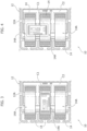
- Conventional semiconductor devices 10 as exemplified in Figures 1 and 2 may comprise plural semiconductor chips (or dice) C1, C2 arranged, whatever their number and functions, at respective adjacent die pads or paddles 12A in a substrate 12 such as leadframe.
- leadframe (or “lead frame”) is currently used (see, for instance the USPC Consolidated Glossary of the United States Patent and Trademark Office) to indicate a metal frame that provides support for an integrated circuit chip or die as well as electrical leads to interconnect the integrated circuit in the die or chip to other electrical components or contacts.
- a leadframe comprises an array of electrically-conductive formations (leads) 12B that from an outline location extend inwardly in the direction of a semiconductor chip or die thus forming an array of electrically-conductive formations from one or more die pads or paddles 12A configured to have at least one semiconductor chip or die attached thereon.
- a die attach adhesive a die attach film or DAF, for instance
- Leadframes are conventionally created using technologies such as a photo-etching technology.
- metal e.g., copper
- metal in the form of a foil or tape is etched on the top and bottom sides to create various pads and leads.
- Substrates such as leadframes are advantageously provided in a pre-molded version wherein an insulating resin (an epoxy resin, for instance) fills the empty spaces between the die pads 12A and leads 12B.
- an insulating resin an epoxy resin, for instance
- a pre-molded leadframe 12 is a thus a laminar substrate that is substantially flat with the pre-mold material (resin) filling the spaces in the electrically conductive structure (of metal material such as copper, for instance) of the leadframe, that has been bestowed a sculptured appearance including empty spaces during forming, by etching, for instance.
- the total thickness of the pre-mold leadframe is the same thickness of the sculptured electrically conductive structure.
- reference 14 indicates so-called “ribbons” (namely narrow strips of electrically conductive materials - copper may be exemplary of such material) providing electrically conductive lines extending over the power dice C2 and configured to carry currents from the power dice C2 to one or more electrical loads (not visible in the figures).
- the ribbons 14 may exhibit a wavy (undulated) pattern that facilitates welding through ultrasonic bonding.
- Power packages as exemplified in Figures 1 and 2 thus include at least two chips or dice.
- These may include, for instance, one or more "power" dice C2 - that provide the power section of the device 10 - and at least one smaller die C1 acting as a controller and connected both to the power die or dice C2 and to the external leads 12B in the substrate (leadframe) 12.
- ribbons such as 14 are primarily used for "heavy duty" lines while the controller die or dice C1 are usually wire bonded with thin wire.
- each die C1, C2 is arranged on a respective die paddle 12A.
- the final package dimensions are dictated by the number and dimensions of the die paddles provided to host the dice C1, C2.
- the number of die mounting positions available in a leadframe is directly linked to the sizes of the individual dice and a higher number of positions becomes available in a leadframe only in the presence of dice of smaller size.
- the positions available in a leadframe can increase, but are still limited by the device package dimension that is linked to the number of dice for each device.
- the final package cost is linked to the package size.
- ribbons 14 used in manufacturing power semiconductor devices as illustrated in Figures 1 and 2 can be rendered strong (rigid and resistant) enough to be used as mounting surfaces for semiconductor dice such as a drive die C1.
- Figure 3 is illustrative of the possibility of mounting (attaching) a small die such as the controller die C1 on a such planar ribbon surface 14A.
- Figure 3 is illustrative of a die C1 of small size capable of being completely accommodated over a planar surface 14A provided in a single one of the ribbons 14.
- That portion of the substrate (lead frame) 12 can be eliminated or used for another purpose as discussed in connection with Figure 7 .
- Figure 4 is exemplary of the fact that the size of the die C1 arranged (attached) on the ribbons 14 is not strictly binding in so far as a (e.g., larger) die as C1 illustrated in dashed outline, can be mounted "astride” or "bridge-like" across two neighboring ribbons 14 (e.g., between two respective planar portions 14A).
- Dice such as C1 can be bonded on top of ribbons 14 using attach materials such as glue or adhesive tape, which may be conductive or non-conductive, depending on the desired application.
- a bridge-like mounting as exemplified in Figure 4 can be exploited (e.g., using electrically conductive material to attach the die C1 on the ribbons 14) to create an electrically conductive path coupling two neighbouring ribbons 14.
- each electrically conductive ribbon 14 extends on one of the first semiconductor dice C2 and each one of the first semiconductor dice C2 lies intermediate the substrate 12 and a respective electrically conductive ribbon 14 in the pair of electrically conductive ribbons 14.
- the at least one second semiconductor die C1 can be arranged bridge-like across the electrically conductive ribbons 14 in the pair to provide a stacked arrangement of the at least one second semiconductor die C1, with each electrically conductive ribbon 14 in the pair of electrically conductive ribbons 14 intermediate a respective one of the first semiconductor dice C2 and one end of the second semiconductor die C1.
- Figure 5 is exemplary of the possibility of mounting plural dice C1 on respective attachment surfaces 14A of two (not necessarily neighbouring) ribbons 14.
- Figures 3 to 5 illustrate (by direct comparison with Figures 1 and 2 ) the possibility of significantly reducing the overall X and Y dimensions of the resulting package.
- This size reduction is beneficial in increasing the number of package positions available on a certain leadframe 12, with the possibility of reducing the final package cost.
- Figure 6 is illustrative of the possibility (along the lines of e.g., Figure 4 ) attaching a die C1 astride or bridge-like between two ribbons 14 and exploiting the space advantage achieved via stacking the chips C1 and C2 to provide an overall reduction of the device package.
- Figure 6 is illustrative of the possibility of attaching a die C1 astride or bridge-like between two ribbons 14 (along the lines of e.g., Figure 4 ) and exploiting the space advantage achieved via stacking the chips C1 and C2 to provide an overall reduction of the device package, by "eliminating" the right-hand portion of the substrate (lead frame) 12 in Figure 1 .
- Figure 7 is exemplary of the possibility of exploiting the space advantage achieved via stacking the chips C1 and C2 to retain the right-hand portion of the substrate (lead frame) 12 in Figure 1 and exploit that portion of the substrate 12 for mounting one or more additional chips or dice as indicated at C3 in dashed outline.
- Figure 6 is exemplary of the possibility of electrically coupling the controller die C1 to the power die C2 via conventional wire bonding 16.
- FIG. 7 illustrates, in addition to that possibility, the possibility of:
- a wire bonding process (as exemplified by the wire bonding lines 16, 18 and 20 of Figure 7 ) can be performed and continued with the other assembly steps (molding and encapsulation, singulation, and so on).
Landscapes
- Die Bonding (AREA)
- Lead Frames For Integrated Circuits (AREA)
- Details Of Connecting Devices For Male And Female Coupling (AREA)
Abstract
Description
- The description relates to semiconductor devices.
- One or more embodiments can be advantageously applied to power semiconductor devices.
- In various power semiconductor devices (including, for instance, power semiconductor devices in a Quad-Flat No-leads or QFN package) one or more power chips or dice are arranged side-by-side with a driver chip or die manufactured, for instance, using BCD (Bipolar-CMOS-DMOS) technology.
- These chips (or dice: the terms "chip" and "die" are used herein as synonyms) can be mounted on respective adjacent die pads or paddles in a leadframe.
- Wire bonding is used to provide die-to-die or die-to-leadframe connections (e.g., signals, ground) and so-called "ribbons" wedge-bonded to the leadframe leads are used to provide conductive lines or paths capable of carrying high currents.
- In such an arrangement, a substantial amount of substrate (leadframe) space is taken by distinct die pads or paddles used for mounting the various power and driver chips or dice.
- Documents such as
US 2012/326287 A1 orUS 2012/119343 A1 are exemplary of the prior art. - An object of one or more embodiments is to contribute in adequately dealing with such an issue.
- According to one or more embodiments, that object is achieved via a method having the features set forth in the claims that follow.
- One or more embodiments relate to a corresponding semiconductor device. A semiconductor device such as a power device comprising plural, mutually coupled semiconductor chips or dice may be exemplary of such a device.
- The claims are an integral part of the technical teaching provided herein in respect of the embodiments.
- One or more embodiments involve stacking at least one die (a driver or controller die, for instance) onto another die (a power die, for instance) by using one or more ribbon sections for attachment.
- In that way, the overall package height is (slightly) increased with the increase largely compensated by a notable reduction in package footprint. This may result in smaller leadframes, smaller packages as well as reduced footprint on final mounting substrates such as printed circuit board (PCBs).
- One or more embodiments thus rely on an unexpected recognition that ribbons such as conventionally used to provide current channels or paths in semiconductor power devices are strong enough to support adequately one or more semiconductor chips attached thereon.
- One or more embodiments offer one or more of the following advantages:
- compatibility with existing wire bonding machines,
- a plug & play process is provided, wherein the number of assembly steps remains substantially unchanged,
- wide applicability to several leadframe packages, package size reduction,
- cost savings due to package size reduction,
- selectivity due to the capability of customising wires and ribbons according to desired specifications.
- As is the case of in conventional arrangements comprising stacked chips, a certain chip (for instance a small one) can be placed "on top" of at least another chip by using a ribbon arranged between as a support structure.
- One or more embodiments thus facilitate reducing the overall X and Y dimensions of a semiconductor chip package with the capability of taking advantage of a possible synergic combination of die bonding, wire bonding and ribbon bonding (plus chip or die stacking) in manufacturing semiconductor devices.
- One or more embodiments will now be described, by way of example only, with reference to the annexed figures, wherein:
-
Figures 1 and 2 are plan views of semiconductor devices comprising plural semiconductor chips arranged on a substrate with ribbons providing power connection channels or paths, -
Figure 3 is a plan view of a semiconductor device according to embodiments of the present description, -
Figure 4 is a plan view of another semiconductor device according to embodiments of the present description, -
Figure 5 is a plan view of still another semiconductor device according to embodiments of the present description, -
Figure 6 is a plan view of a further semiconductor device according to embodiments of the present description, and -
Figure 7 is a plan view exemplary of a possible variant of the example presented inFigure 6 . - Corresponding numerals and symbols in the different figures generally refer to corresponding parts unless otherwise indicated.
- The figures are drawn to clearly illustrate the relevant aspects of the embodiments and are not necessarily drawn to scale.
- The edges of features drawn in the figures do not necessarily indicate the termination of the extent of the feature.
- In the ensuing description, various specific details are illustrated in order to provide an in-depth understanding of various examples of embodiments according to the description. The embodiments may be obtained without one or more of the specific details, or with other methods, components, materials, etc. In other cases, known structures, materials, or operations are not illustrated or described in detail so that various aspects of the embodiments will not be obscured.
- Reference to "an embodiment" or "one embodiment" in the framework of the present description is intended to indicate that a particular configuration, structure, or characteristic described in relation to the embodiment is comprised in at least one embodiment. Hence, phrases such as "in an embodiment", "in one embodiment", or the like, that may be present in various points of the present description do not necessarily refer exactly to one and the same embodiment. Furthermore, particular configurations, structures, or characteristics may be combined in any adequate way in one or more embodiments.
- The headings/references used herein are provided merely for convenience and hence do not define the extent of protection or the scope of the embodiments.
-
Conventional semiconductor devices 10 as exemplified inFigures 1 and 2 may comprise plural semiconductor chips (or dice) C1, C2 arranged, whatever their number and functions, at respective adjacent die pads orpaddles 12A in asubstrate 12 such as leadframe. - The designation "leadframe" (or "lead frame") is currently used (see, for instance the USPC Consolidated Glossary of the United States Patent and Trademark Office) to indicate a metal frame that provides support for an integrated circuit chip or die as well as electrical leads to interconnect the integrated circuit in the die or chip to other electrical components or contacts.
- Essentially, a leadframe comprises an array of electrically-conductive formations (leads) 12B that from an outline location extend inwardly in the direction of a semiconductor chip or die thus forming an array of electrically-conductive formations from one or more die pads or
paddles 12A configured to have at least one semiconductor chip or die attached thereon. - This may be via conventional means such as a die attach adhesive (a die attach film or DAF, for instance) .
- Leadframes are conventionally created using technologies such as a photo-etching technology. With this technology, metal (e.g., copper) material in the form of a foil or tape is etched on the top and bottom sides to create various pads and leads.
- Substrates such as leadframes are advantageously provided in a pre-molded version wherein an insulating resin (an epoxy resin, for instance) fills the empty spaces between the
die pads 12A and leads 12B. - A
pre-molded leadframe 12 is a thus a laminar substrate that is substantially flat with the pre-mold material (resin) filling the spaces in the electrically conductive structure (of metal material such as copper, for instance) of the leadframe, that has been bestowed a sculptured appearance including empty spaces during forming, by etching, for instance. - The total thickness of the pre-mold leadframe is the same thickness of the sculptured electrically conductive structure.
- In
Figures 1 and 2 reference 14 indicates so-called "ribbons" (namely narrow strips of electrically conductive materials - copper may be exemplary of such material) providing electrically conductive lines extending over the power dice C2 and configured to carry currents from the power dice C2 to one or more electrical loads (not visible in the figures). - As illustrated in
Figures 1 and 2 , theribbons 14 may exhibit a wavy (undulated) pattern that facilitates welding through ultrasonic bonding. - Power packages as exemplified in
Figures 1 and 2 thus include at least two chips or dice. - These may include, for instance, one or more "power" dice C2 - that provide the power section of the device 10 - and at least one smaller die C1 acting as a controller and connected both to the power die or dice C2 and to the
external leads 12B in the substrate (leadframe) 12. - As noted, ribbons such as 14 are primarily used for "heavy duty" lines while the controller die or dice C1 are usually wire bonded with thin wire.
- In conventional arrangements as illustrated in
Figures 1 and 2 , each die C1, C2 is arranged on arespective die paddle 12A. - Consequently, the final package dimensions are dictated by the number and dimensions of the die paddles provided to host the dice C1, C2.
- From a package perspective, this translates into a larger package size as the number of dice increases as is currently the case with power applications comprising multi-die packages.
- Stated otherwise, in conventional arrangements as illustrated in
Figures 1 and 2 - where the dice C1, C2 are arranged mutually adjacent - an increased number of dice C1, C2 leads to more space required and larger X and Y dimensions of the device package, with the final package dimensions inevitably increased. - In a complementary manner, the number of die mounting positions available in a leadframe is directly linked to the sizes of the individual dice and a higher number of positions becomes available in a leadframe only in the presence of dice of smaller size.
- If the dice have a smaller size, the positions available in a leadframe can increase, but are still limited by the device package dimension that is linked to the number of dice for each device.
- The final package cost is linked to the package size.
- The possibility of stacking chips or dice (e.g., by stacking a smaller die "on top" of a larger die) is well known in the art.
- On the other hand, looking at
Figures 1 and 2 , and thinking of, e.g., stacking the die C1 on the or one of the dice C2 one would inevitably conclude that theribbons 14 that extend over the dice C2 militate against such a solution. - This is particularly the case if one considers the general wavy pattern bestowed upon the
ribbons 14 in order to facilitate welding thereof, e.g., through ultrasonic bonding. - Contrary to such expectations,
ribbons 14 used in manufacturing power semiconductor devices as illustrated inFigures 1 and 2 can be rendered strong (rigid and resistant) enough to be used as mounting surfaces for semiconductor dice such as a drive die C1. - This may be particularly the case if (as illustrated in Figures starting from
Figure 3 onwards) the or each of theribbons 14 used for mounting a die C1 thereon are shaped (in a manner otherwise known to those of skill in the art of ribbon bonding) in such a way to exhibit a planar surface as exemplified at 14A inFigures 3 to 7 . - It is again noted that throughout these figures, parts or elements like or similar to parts or elements already discussed in connection with
Figures 1 and 2 are indicated with the same reference symbols: a corresponding detailed description will not be repeated for brevity. -
Figure 3 is illustrative of the possibility of mounting (attaching) a small die such as the controller die C1 on a suchplanar ribbon surface 14A. - This may occur via a conventional attachment material ("glue") as known to those of skill in the art.
-
Figure 3 is illustrative of a die C1 of small size capable of being completely accommodated over aplanar surface 14A provided in a single one of theribbons 14. - By comparing
Figure 3 withFigure 1 one may note that, with the die C1 mounted on one of theribbons 14 in turn extending over the die or dice C2 - as illustrated inFigure 3 - the portion of the substrate (lead frame) 12 that inFigure 1 hosts the die C1 (including thedie pad 12A on the right hand of the figure) is no longer used for mounting the die C1. - That portion of the substrate (lead frame) 12 can be eliminated or used for another purpose as discussed in connection with
Figure 7 . -
Figure 4 is exemplary of the fact that the size of the die C1 arranged (attached) on theribbons 14 is not strictly binding in so far as a (e.g., larger) die as C1 illustrated in dashed outline, can be mounted "astride" or "bridge-like" across two neighboring ribbons 14 (e.g., between two respectiveplanar portions 14A). - Dice such as C1 can be bonded on top of
ribbons 14 using attach materials such as glue or adhesive tape, which may be conductive or non-conductive, depending on the desired application. - A bridge-like mounting as exemplified in
Figure 4 can be exploited (e.g., using electrically conductive material to attach the die C1 on the ribbons 14) to create an electrically conductive path coupling two neighbouringribbons 14. - For instance, one can arrange on the substrate 12 a pair of adjacent first semiconductor dice C2 with a pair of electrically
conductive ribbons 14. Each electricallyconductive ribbon 14 extends on one of the first semiconductor dice C2 and each one of the first semiconductor dice C2 lies intermediate thesubstrate 12 and a respective electricallyconductive ribbon 14 in the pair of electricallyconductive ribbons 14. - The at least one second semiconductor die C1 can be arranged bridge-like across the electrically
conductive ribbons 14 in the pair to provide a stacked arrangement of the at least one second semiconductor die C1, with each electricallyconductive ribbon 14 in the pair of electricallyconductive ribbons 14 intermediate a respective one of the first semiconductor dice C2 and one end of the second semiconductor die C1. - For instance, one can attach the at least one second semiconductor die C1 bridge-like across the electrically
conductive ribbons 14 in the pair via electrically conductive attach material so that the electricallyconductive ribbons 14 are mutually electrically coupled. - A somewhat similar arrangement is disclosed in
European patent application 22181327.2 -
Figure 5 is exemplary of the possibility of mounting plural dice C1 on respective attachment surfaces 14A of two (not necessarily neighbouring)ribbons 14. - Whatever the arrangement adopted for attachment, solutions as illustrated is
Figures 3 to 5 illustrate (by direct comparison withFigures 1 and 2 ) the possibility of significantly reducing the overall X and Y dimensions of the resulting package. - This size reduction is beneficial in increasing the number of package positions available on a
certain leadframe 12, with the possibility of reducing the final package cost. - This possibility is exemplified by the comparison of
Figures 6 and7 . -
Figure 6 is illustrative of the possibility (along the lines of e.g.,Figure 4 ) attaching a die C1 astride or bridge-like between tworibbons 14 and exploiting the space advantage achieved via stacking the chips C1 and C2 to provide an overall reduction of the device package. -
Figure 6 is illustrative of the possibility of attaching a die C1 astride or bridge-like between two ribbons 14 (along the lines of e.g.,Figure 4 ) and exploiting the space advantage achieved via stacking the chips C1 and C2 to provide an overall reduction of the device package, by "eliminating" the right-hand portion of the substrate (lead frame) 12 inFigure 1 . -
Figure 7 is exemplary of the possibility of exploiting the space advantage achieved via stacking the chips C1 and C2 to retain the right-hand portion of the substrate (lead frame) 12 inFigure 1 and exploit that portion of thesubstrate 12 for mounting one or more additional chips or dice as indicated at C3 in dashed outline. - An essentially similar approach can be applied to the arrangement of
Figure 2 , where the place "left free" by the die C1 mounted on one or more of theribbons 14 on the left-hand side of the figure possibly used to mount another die. - Also,
Figure 6 is exemplary of the possibility of electrically coupling the controller die C1 to the power die C2 viaconventional wire bonding 16. -
Figure 7 illustrates, in addition to that possibility, the possibility of: - electrically coupling the power die C2 to
external leads 12B in the leadframe viafurther wire bonds 18; and - electrically coupling the controller die C1 to
external leads 12B in the leadframe via further wire bonds 20. - It will be appreciated that referring to the dice C1 and C2 as controller and power dice is purely exemplary: one or more embodiments may in fact apply irrespective of the nature and the type of the chips or dice involved.
- While "functional" ribbons such as 14 (namely ribbons intended to provide high current flow channels or paths for the device 10) have been exemplified herein, certain examples may contemplate providing "dummy" ribbons (that is, ribbons that per se are not necessitated by any electrical connection) in order to facilitate arranging a chip or die thereon, possibly in a bridge-like arrangement with a "functional" ribbon.
- Conventional metal materials (aluminum, copper or gold, for instance) as currently used in providing ribbons in semiconductor power devices were found to be adequate for the embodiments, that is, adequate for producing ribbons strong enough to support a semiconductor die such as C1 mounted thereon, with the capability of having planar portions such as 14A formed therein.
- The examples herein have no appreciable impact on the assembly flow of the
device 10. - In fact, after die bonding on one or more ribbons (as previously formed to provide power lines as desired) a wire bonding process (as exemplified by the
wire bonding lines Figure 7 ) can be performed and continued with the other assembly steps (molding and encapsulation, singulation, and so on). - Without prejudice to the underlying principles, the details and the embodiments may vary, even significantly, with respect to what has been described by way of example only without departing from the scope of the embodiments.
- The extent of protection is determined by the annexed claims.
Claims (12)
- A method, comprising:arranging on a die pad (12A) in a substrate (12) at least one first semiconductor die (C2) with at least one electrically conductive ribbon (14) extending on the at least one first semiconductor die (C2) wherein the at least one first semiconductor die (C2) lies intermediate the substrate (12) and the at least one electrically conductive ribbon (14), andattaching at least one second semiconductor die (C1) on the at least one electrically conductive ribbon (14) to provide on said die pad (12A) a stacked arrangement of the at least one second semiconductor die (C1) and the at least one first semiconductor die (C2) with the at least one electrically conductive ribbon (14) intermediate the at least one first semiconductor die (C2) and the at least one second semiconductor die (C1).
- The method of claim 1, comprising:arranging on said substrate (12) a pair of adjacent first semiconductor dice (C2) with a pair of electrically conductive ribbons (14) each electrically conductive ribbon (14) extending on one of the first semiconductor dice (C2), wherein each one of the first semiconductor dice (C2) lies intermediate the substrate (12) and a respective electrically conductive ribbon (14) in the pair of electrically conductive ribbons (14), andattaching the at least one second semiconductor die (C1) bridge-like across said electrically conductive ribbons (14) in said pair of electrically conductive ribbons (14) to provide a stacked arrangement of the at least one second semiconductor die (C1), with each electrically conductive ribbon (14) in the pair of electrically conductive ribbons (14) intermediate a respective one of the first semiconductor dice (C2) and one end of the second semiconductor die (C1).
- The method of claim 2, comprising attaching the at least one second semiconductor die (C1) bridge-like across said electrically conductive ribbons (14) in said pair of electrically conductive ribbons (14) via electrically conductive attach material wherein said electrically conductive ribbons (14) are mutually electrically coupled.
- The method of any of the previous claims, wherein the at least electrically conductive ribbon (14) has a wavy pattern and wherein the method comprises providing at least one planar portion (14A) in the electrically conductive ribbon (14) and attaching the at least one second semiconductor die (C1) on the at least one planar portion (14A) in the electrically conductive ribbon (14) .
- The method of any of the previous claims, comprising:providing in said substrate (12) a further die pad (12A) adjacent to said die pad (12A), andattaching on said further die pad (12A) at least one third semiconductor die (C3).
- The method of any of the previous claims, comprising at least one of:a first wire-bond pattern (16) mutually coupling the at least one first semiconductor die (C2) and the at least one second semiconductor die (C1) in said stacked arrangement of the at least one second semiconductor die (C1) and the at least one first semiconductor die (C2), and/ora second wirebond pattern (18) coupling said at least one first semiconductor die (C2) with electrically conductive formations (12B) in an array of electrically conductive formations provided in said substrate (12) around said die pad (12A), and/ora third wirebond pattern (20) coupling said at least one second semiconductor die (C1) with electrically conductive formations (12B) in an array of electrically conductive formations provided in said substrate (12) around said die pad (12A).
- A device (10), comprising:a substrate (12) comprising a die pad (12A) having arranged thereon at least one first semiconductor die (C2) with at least one electrically conductive ribbon (14) extending on the at least one first semiconductor die (C2) wherein the at least one first semiconductor die (C2) lies intermediate the substrate (12) and the at least one electrically conductive ribbon (14), andat least one second semiconductor die (C1) on the at least one electrically conductive ribbon (14) to provide on said die pad (12A) a stacked arrangement of the at least one second semiconductor die (C1) and the at least one first semiconductor die (C2) with the at least one electrically conductive ribbon (14) intermediate the at least one first semiconductor die (C2) and the at least one second semiconductor die (C1).
- The device (10) of claim 7, comprising:a pair of adjacent first semiconductor dice (C2) arranged on said substrate (12) with a pair of electrically conductive ribbons (14) each electrically conductive ribbon (14) extending on one of the first semiconductor dice (C2), wherein each one of the first semiconductor dice (C2) lies intermediate the substrate (12) and a respective electrically conductive ribbon (14) in the pair of electrically conductive ribbons (14), andat least one second semiconductor die (C1) attached bridge-like across said electrically conductive ribbons (14) in said pair of electrically conductive ribbons (14) to provide a stacked arrangement of the at least one second semiconductor die (C1), with each electrically conductive ribbon (14) in the pair of electrically conductive ribbons (14) intermediate a respective one of the first semiconductor dice (C2) and one end of the second semiconductor die (C1).
- The device (10) of claim 8, comprising the at least one second semiconductor die (C1) attached bridge-like across said electrically conductive ribbons (14) in said pair of electrically conductive ribbons (14) via electrically conductive attach material wherein said electrically conductive ribbons (14) are mutually electrically coupled.
- The device (10) of any of claims 7 to 9, wherein the at least electrically conductive ribbon (14) has a wavy pattern with at least one planar portion (14A) in the electrically conductive ribbon (14), wherein the at least one second semiconductor die (C1) is attached to the at least one planar portion (14A) in the electrically conductive ribbon (14).
- The device (10) of any of claims 7 to 10, comprising:a further die pad (12A) provided in said substrate (12) adjacent said die pad (12A), andat least one third semiconductor die (C3) attaching on said further die pad (12A)
- The device (10) of any of claims 7 to 11, comprising at least one of:a first wire-bond pattern (16) mutually coupling the at least one first semiconductor die (C2) and the at least one second semiconductor die (C1) in said stacked arrangement of the at least one second semiconductor die (C1) and the at least one first semiconductor die (C2), and/ora second wirebond pattern (18) coupling said at least one first semiconductor die (C2) with electrically conductive formations (12B) in an array of electrically conductive formations provided in said substrate (12) around said a die pad (12A), and/ora third wirebond pattern (20) coupling said at least one second semiconductor die (C1) with electrically conductive formations (12B) in an array of electrically conductive formations provided in said substrate (12) around said a die pad (12A).
Applications Claiming Priority (1)
| Application Number | Priority Date | Filing Date | Title |
|---|---|---|---|
| IT102021000020552A IT202100020552A1 (en) | 2021-07-30 | 2021-07-30 | PROCEDURE FOR ASSEMBLING SEMICONDUCTOR DEVICES AND CORRESPONDING SEMICONDUCTOR DEVICE |
Publications (1)
| Publication Number | Publication Date |
|---|---|
| EP4125122A1 true EP4125122A1 (en) | 2023-02-01 |
Family
ID=78049706
Family Applications (1)
| Application Number | Title | Priority Date | Filing Date |
|---|---|---|---|
| EP22187591.7A Pending EP4125122A1 (en) | 2021-07-30 | 2022-07-28 | Method of assembling semiconductor devices and corresponding semiconductor device |
Country Status (4)
| Country | Link |
|---|---|
| US (1) | US12506053B2 (en) |
| EP (1) | EP4125122A1 (en) |
| CN (2) | CN115692225A (en) |
| IT (1) | IT202100020552A1 (en) |
Families Citing this family (2)
| Publication number | Priority date | Publication date | Assignee | Title |
|---|---|---|---|---|
| IT202100020552A1 (en) | 2021-07-30 | 2023-01-30 | St Microelectronics Srl | PROCEDURE FOR ASSEMBLING SEMICONDUCTOR DEVICES AND CORRESPONDING SEMICONDUCTOR DEVICE |
| US12575468B2 (en) * | 2021-10-07 | 2026-03-10 | Stmicroelectronics S.R.L. | Roughened surface of a conductive wedge bonded ribbon encapsulated in a sermiconductor package |
Citations (2)
| Publication number | Priority date | Publication date | Assignee | Title |
|---|---|---|---|---|
| US20120119343A1 (en) | 2009-10-16 | 2012-05-17 | Texas Instruments Incorporated | Stacked leadframe implementation for dc/dc convertor power module incorporating a stacked controller and stacked leadframe construction methodology |
| US20120326287A1 (en) | 2011-06-27 | 2012-12-27 | National Semiconductor Corporation | Dc/dc convertor power module package incorporating a stacked controller and construction methodology |
Family Cites Families (6)
| Publication number | Priority date | Publication date | Assignee | Title |
|---|---|---|---|---|
| US7443018B2 (en) | 2005-11-09 | 2008-10-28 | Stats Chippac Ltd. | Integrated circuit package system including ribbon bond interconnect |
| JP2009231805A (en) | 2008-02-29 | 2009-10-08 | Renesas Technology Corp | Semiconductor device |
| US9082868B2 (en) | 2013-03-13 | 2015-07-14 | Semiconductor Components Industries, Llc | Semiconductor component and method of manufacture |
| KR101983165B1 (en) | 2013-12-26 | 2019-05-28 | 삼성전기주식회사 | Semiconductor package |
| JP7173487B2 (en) | 2018-11-30 | 2022-11-16 | ローム株式会社 | semiconductor equipment |
| IT202100020552A1 (en) | 2021-07-30 | 2023-01-30 | St Microelectronics Srl | PROCEDURE FOR ASSEMBLING SEMICONDUCTOR DEVICES AND CORRESPONDING SEMICONDUCTOR DEVICE |
-
2021
- 2021-07-30 IT IT102021000020552A patent/IT202100020552A1/en unknown
-
2022
- 2022-07-26 US US17/873,749 patent/US12506053B2/en active Active
- 2022-07-28 EP EP22187591.7A patent/EP4125122A1/en active Pending
- 2022-07-29 CN CN202210909307.8A patent/CN115692225A/en active Pending
- 2022-07-29 CN CN202221986369.0U patent/CN218957727U/en active Active
Patent Citations (2)
| Publication number | Priority date | Publication date | Assignee | Title |
|---|---|---|---|---|
| US20120119343A1 (en) | 2009-10-16 | 2012-05-17 | Texas Instruments Incorporated | Stacked leadframe implementation for dc/dc convertor power module incorporating a stacked controller and stacked leadframe construction methodology |
| US20120326287A1 (en) | 2011-06-27 | 2012-12-27 | National Semiconductor Corporation | Dc/dc convertor power module package incorporating a stacked controller and construction methodology |
Also Published As
| Publication number | Publication date |
|---|---|
| US20230032786A1 (en) | 2023-02-02 |
| CN218957727U (en) | 2023-05-02 |
| US12506053B2 (en) | 2025-12-23 |
| IT202100020552A1 (en) | 2023-01-30 |
| CN115692225A (en) | 2023-02-03 |
Similar Documents
| Publication | Publication Date | Title |
|---|---|---|
| US6927483B1 (en) | Semiconductor package exhibiting efficient lead placement | |
| US8410585B2 (en) | Leadframe and semiconductor package made using the leadframe | |
| JP3118167B2 (en) | Electronic package and manufacturing method thereof | |
| US6420783B2 (en) | Semiconductor device and a method of manufacturing the same | |
| US9184142B2 (en) | Semiconductor device and manufacturing method of the same | |
| US12506053B2 (en) | Method of assembling semiconductor devices and corresponding semiconductor device | |
| WO2007011511A2 (en) | Die package with asymmetric leadframe connection | |
| US7436049B2 (en) | Lead frame, semiconductor chip package using the lead frame, and method of manufacturing the semiconductor chip package | |
| JP2637247B2 (en) | Resin-sealed semiconductor device | |
| US20130200507A1 (en) | Two-sided die in a four-sided leadframe based package | |
| US6686651B1 (en) | Multi-layer leadframe structure | |
| EP4113600B1 (en) | Method of manufacturing semiconductor devices and corresponding semiconductor device | |
| KR20040108582A (en) | Seniconductor device and method for fabricating the same | |
| US8349655B2 (en) | Method of fabricating a two-sided die in a four-sided leadframe based package | |
| US20030119224A1 (en) | Semiconductor package | |
| US12463170B2 (en) | Semiconductor device and assortment of semiconductor devices with electrically conductive ribbon configurations | |
| CN102709199B (en) | Mold array process method for covering side edge of substrate | |
| EP4016617A1 (en) | Method of manufacturing semiconductor devices, component for use therein and corresponding semiconductor device | |
| EP4489070A1 (en) | Method of manufacturing semiconductor devices, corresponding pre-molded leadframe and semiconductor device | |
| US20230170283A1 (en) | Method of manufacturing semiconductor devices and corresponding semiconductor device | |
| EP4517819A1 (en) | Method of manufacturing semiconductor devices, corresponding component and semiconductor device | |
| EP4411814A1 (en) | Method of manufacturing semiconductor devices, corresponding ribbon, apparatus and device | |
| EP4365943A1 (en) | Method of manufacturing semiconductor devices, corresponding component, semiconductor device and method | |
| JP3938525B2 (en) | Manufacturing method of semiconductor device | |
| CN119275100A (en) | Method for manufacturing a semiconductor device, corresponding pre-molded lead frame and semiconductor device |
Legal Events
| Date | Code | Title | Description |
|---|---|---|---|
| PUAI | Public reference made under article 153(3) epc to a published international application that has entered the european phase |
Free format text: ORIGINAL CODE: 0009012 |
|
| STAA | Information on the status of an ep patent application or granted ep patent |
Free format text: STATUS: THE APPLICATION HAS BEEN PUBLISHED |
|
| AK | Designated contracting states |
Kind code of ref document: A1 Designated state(s): AL AT BE BG CH CY CZ DE DK EE ES FI FR GB GR HR HU IE IS IT LI LT LU LV MC MK MT NL NO PL PT RO RS SE SI SK SM TR |
|
| STAA | Information on the status of an ep patent application or granted ep patent |
Free format text: STATUS: REQUEST FOR EXAMINATION WAS MADE |
|
| 17P | Request for examination filed |
Effective date: 20230710 |
|
| RBV | Designated contracting states (corrected) |
Designated state(s): AL AT BE BG CH CY CZ DE DK EE ES FI FR GB GR HR HU IE IS IT LI LT LU LV MC MK MT NL NO PL PT RO RS SE SI SK SM TR |