EP4125121A1 - Method of manufacturing substrates for semiconductor devices, corresponding substrate and semiconductor device - Google Patents
Method of manufacturing substrates for semiconductor devices, corresponding substrate and semiconductor device Download PDFInfo
- Publication number
- EP4125121A1 EP4125121A1 EP22187296.3A EP22187296A EP4125121A1 EP 4125121 A1 EP4125121 A1 EP 4125121A1 EP 22187296 A EP22187296 A EP 22187296A EP 4125121 A1 EP4125121 A1 EP 4125121A1
- Authority
- EP
- European Patent Office
- Prior art keywords
- die pad
- anchoring formations
- mold material
- anchoring
- formations
- Prior art date
- Legal status (The legal status is an assumption and is not a legal conclusion. Google has not performed a legal analysis and makes no representation as to the accuracy of the status listed.)
- Granted
Links
Images


Classifications
-
- H—ELECTRICITY
- H10—SEMICONDUCTOR DEVICES; ELECTRIC SOLID-STATE DEVICES NOT OTHERWISE PROVIDED FOR
- H10W—GENERIC PACKAGES, INTERCONNECTIONS, CONNECTORS OR OTHER CONSTRUCTIONAL DETAILS OF DEVICES COVERED BY CLASS H10
- H10W70/00—Package substrates; Interposers; Redistribution layers [RDL]
- H10W70/40—Leadframes
- H10W70/479—Leadframes on or in insulating or insulated package substrates, interposers, or redistribution layers
-
- H—ELECTRICITY
- H10—SEMICONDUCTOR DEVICES; ELECTRIC SOLID-STATE DEVICES NOT OTHERWISE PROVIDED FOR
- H10W—GENERIC PACKAGES, INTERCONNECTIONS, CONNECTORS OR OTHER CONSTRUCTIONAL DETAILS OF DEVICES COVERED BY CLASS H10
- H10W70/00—Package substrates; Interposers; Redistribution layers [RDL]
- H10W70/01—Manufacture or treatment
- H10W70/04—Manufacture or treatment of leadframes
- H10W70/047—Attaching leadframes to insulating supports, e.g. for tape automated bonding [TAB]
-
- H—ELECTRICITY
- H10—SEMICONDUCTOR DEVICES; ELECTRIC SOLID-STATE DEVICES NOT OTHERWISE PROVIDED FOR
- H10W—GENERIC PACKAGES, INTERCONNECTIONS, CONNECTORS OR OTHER CONSTRUCTIONAL DETAILS OF DEVICES COVERED BY CLASS H10
- H10W70/00—Package substrates; Interposers; Redistribution layers [RDL]
- H10W70/40—Leadframes
- H10W70/411—Chip-supporting parts, e.g. die pads
-
- H—ELECTRICITY
- H10—SEMICONDUCTOR DEVICES; ELECTRIC SOLID-STATE DEVICES NOT OTHERWISE PROVIDED FOR
- H10W—GENERIC PACKAGES, INTERCONNECTIONS, CONNECTORS OR OTHER CONSTRUCTIONAL DETAILS OF DEVICES COVERED BY CLASS H10
- H10W70/00—Package substrates; Interposers; Redistribution layers [RDL]
- H10W70/40—Leadframes
- H10W70/421—Shapes or dispositions
- H10W70/435—Shapes or dispositions of insulating layers on leadframes, e.g. bridging members
Definitions
- the description relates to semiconductor devices.
- One or more embodiments can be applied to semiconductor power devices for the automotive sector, for instance.
- pads in pre-molded leadframes should desirably resist pressing forces (as developed, e.g., during ribbon ultrasonic wedge bonding) as well as pulling forces (as developed, e.g., during ribbon pulling for second bond, or as a result thermo-mechanical stress under operation).
- slot-like anchoring structures provide limited pulling resistance while taking a non-negligible pad area.
- An object of one or more embodiments is to deal with the issues as discussed in the foregoing.
- One or more embodiments relate to a corresponding substrate (leadframe) for semiconductor devices.
- One or more embodiments relate to a semiconductor device.
- One or more embodiments provide a die pad design for a pre-molded leadframe (formed through standard half-etch before pre-molding, by a leadframe supplier, for instance) comprising an alternation of 'fingernail-like' anchoring structures on the top and bottom sides of the die pad.
- references to "an embodiment” or “one embodiment” in the framework of the present description is intended to indicate that a particular configuration, structure, or characteristic described in relation to the embodiment is comprised in at least one embodiment.
- phrases such as “in an embodiment”, “in one embodiment”, or the like, that may be present in various points of the present description do not necessarily refer exactly to one and the same embodiment.
- particular configurations, structures, or characteristics may be combined in any adequate way in one or more embodiments.
- Semiconductor devices may comprise one or more semiconductor chips or dice arranged (attached) on substrates such as leadframes.
- Plastic packages are commonly used for semiconductor devices. Such packages may include a leadframe providing a base substrate comprising electrically conductive material such as copper, sized and shaped to accommodate semiconductor chips or dice and providing pad connections (leads) for these chips or dice.
- leadframe (or “lead frame”) is currently used (see, for instance the USPC Consolidated Glossary of the United States Patent and Trademark Office) to indicate a metal frame that provides support for an integrated circuit chip or die as well as electrical leads to interconnect the integrated circuit in the die or chip to other electrical components or contacts.
- Leadframes are conventionally created using technologies such as a photo-etching technology.
- metal e.g., copper
- metal in the form of a foil or tape is etched on the top and bottom sides to create various pads and leads.
- Substrates such as leadframes are advantageously provided in a pre-molded version wherein an insulating resin (an epoxy resin, for instance) fills the empty spaces between the die pads and leads.
- an insulating resin an epoxy resin, for instance
- a pre-molded leadframe is a thus a laminar substrate that is substantially flat with the pre-mold material (resin) filling the spaces in the electrically conductive structure (metal material such as copper, for instance) of the leadframe, that has been bestowed a sculptured appearance including empty spaces during forming, by etching, for instance.
- the total thickness of the pre-mold leadframe is the same thickness of the sculptured electrically conductive structure.
- a pre-molded leadframe can be exposed to repeated stress.
- pads in pre-molded leadframes are exposed to pressing forces (as developed, e.g., during ribbon ultrasonic wedge bonding) as well as to pulling forces (as developed, e.g., during ribbon pulling for second bond, or as a result of thermo-mechanical stress under operation).
- Figure 1 is a cross-sectional view of a portion of a conventional pre-molded leadframe illustrated as comprising, in general, electrically conductive (metal, e.g., copper) portions 10 included in a sculptured, electrically conductive structure of the leadframe (not visible in its entirety), having spaces filled by the pre-mold material (resin) 12.
- electrically conductive metal, e.g., copper
- a pre-molded leaframe PLF as illustrated in Figure 1 has opposite first and second die pad surfaces 10A and 10B, with the first surfaces 10A configured to have at least one semiconductor chip mounted thereon.
- Figure 1 is thus exemplary of a conventional approach wherein a sculptured, electrically conductive laminar structure is provided having spaces therein, the laminar structure including one or more die pads 10 having a first die pad surface 10A configured to have at least one semiconductor chip mounted thereon as well as a second die pad surface 10B opposite the first die pad surface 10A.
- Figure 1 is likewise exemplary of a conventional approach wherein pre-mold material 12 is molded onto the laminar structure 10.
- the pre-mold material 12 penetrates into the spaces formed (e.g., etched) in the sculptured, electrically conductive laminar structure and provides a laminar pre-molded substrate PLF, 10, 12 including one or more die pads left exposed by the pre-mold material 12 at the first surface 10A with the periphery of the die pad or pads 10 bordering on the pre-mold material 12 molded onto the laminar structure.
- the sculpturing bestowed on the electrically conductive (metal, e.g., copper) portions 10 of the (pre-molded) leadframe is beneficial in keeping all the leadframe parts (leads and die pads) together in a robust structure to facilitate the subsequent process steps.
- These steps may include, for instance - after attaching one or more chips or dice on the die pad or pads in the leadframe 10, 12 and the chips or dice being electrically bonded to the leads in the leadframe (not explicitly visible in Figure 1 ) - a molding resin being molded to provide an insulating encapsulation of a final device.
- Figure 1 is exemplary of a leadframe for, e.g., a Quad-Flat No-leads (QFN) device where the sculptured, electrically conductive structure of the leadframe is half etched, that is, a part of copper material is removed, e.g., at the periphery of die pad so that (as visible in Figure 1 ) the die pad is larger at the front or top surface 10A of the leadframe than at the back or bottom surface 10B of the leadframe.
- QFN Quad-Flat No-leads
- Half etching can be performed in any manner known to those of skill in the art.
- the die pad being larger at the front or top surface 10A than at the back or bottom surface 10B as illustrated in Figure 1 increases the molding adhesion around the leadframe parts. This is due to a step-like interface formed between the conductive (metal, e.g., copper) portions 10 of the leadframe and the pre-mold material (resin) 12 molded thereon.
- conductive metal, e.g., copper
- this design results in increased resistance to detachment (delamination) between the conductive portions 10 of the leadframe and the non-conductive pre-mold material 12 molded thereon as possibly induced by "pulling” forces F1 (namely forces urging the metal part 10 shown in Figure 1 in the direction from the back or bottom surface 10B towards the front or top surface 10A) and by “pushing” or “pressing” forces F2 (namely forces urging the metal part 10 shown in Figure 1 in the direction from the front or top surface 10A towards the back or bottom surface 10B).
- "pulling” forces F1 namely forces urging the metal part 10 shown in Figure 1 in the direction from the back or bottom surface 10B towards the front or top surface 10A
- F2 namely forces urging the metal part 10 shown in Figure 1 in the direction from the front or top surface 10A towards the back or bottom surface 10B.
- Such a step-like interface includes undercuts as indicated at 120 where the periphery of the conductive portion 10 of the leadframe abuts against the pre-mold material (resin) 12.
- This provides a form coupling such that the resistance to "pushing" forces F2 (directed downwards in Figure 1 ) is inevitably (much) higher than the resistance to "pulling” forces F1 (directed upwards in Figure 1 ).
- Forces applied to a pre-molded leadframe such as 10, 12 in Figure 1 during the assembly flow of a semiconductor device include both pressing forces such as, e.g., pressing forces applied during ribbon bonding by a bonding tool together with ultrasonic vibrations and pulling forces, e.g., when a ribbon is pulled or cut by moving or opening a bonding cutting tool.
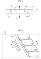
- Figure 2 and Figures 3A and 3B illustrate a solution as disclosed in US 2021/193591 A1 (to which EP 3 840 040 A1 corresponds) assigned to the same Assignee of the present application.
- the leadframe of US 2021/193591 A1 comprises a die pad portion having a first planar die-mounting surface 10A and a second planar surface 10B opposed the first surface 10A.
- the die pad surfaces 10A and 10B have facing peripheral rims jointly defining a peripheral outline of the die pad.
- At least one cavity 100 is provided extending through the die pad from the first planar surface 10A to the second planar surface 10B to define an anchoring portion of the die pad positioned between said at least one cavity and the peripheral outline.
- a first etched part extends into the first planar die-mounting surface 10A to a first depth less than a thickness of the die pad and a second etched part extends into the second planar surface to a second depth less than the thickness of the die pad.
- the first etched part defines a step surface within the cavity 100 that extends parallel to the first planar die-mounting surface 10A and the second etched part defines a thickness of the anchoring portion which is less than the thickness of the die pad.
- Figures 3A and 3B (where the pre-mold material 12 is visible, filling the spaces in the sculptured, electrically conductive structure 10 of the leadframe) show that such an arrangement may lead to the formations of undercuts 120, 120' facing in opposite directions.
- undercuts 120 and 120' provide a form coupling of the electrically conductive structure 10 of the leadframe and the pre-mold material 12 providing improved resistance also to pulling forces F1 ( Figure 3A ) in addition is pushing or pressing forces F2 ( Figure 3B ) .
- the resistance to pushing forces F2 may end up by being higher than the resistance to pulling forces F1, while for certain applications having a resistance to pulling forces F1 equal or possibly higher than the resistance to pushing or pressing forces F2 may be a desirable feature.
- cavities/apertures such as 100 in Figures 2 , 3A and 3B subtract area that should be desirably left available for die attachment.
- Examples as presented in Figures 4 to 7 comprise, in the place of a half-etched step-like metal-to-resin interface (as illustrated in Figure 1 ) or slots (such as 100 in Figure 2 ), an alternation or series of (e.g., fingernail-like) cutaway portions 200A, 200B formed along the border (that is, along the peripheral edge) of the die pad 10, advantageously all around the die pad 10.
- a half-etched step-like metal-to-resin interface as illustrated in Figure 1
- slots such as 100 in Figure 2
- cutaway portions 200A, 200B that are arranged alternatively (possibly alternately) at the front or top surface 10A and at the back or bottom surface 10B, are filled by the pre-mold resin 12 creating (once the resin is solidified, e.g., via thermosetting) a robust structure of the pre-molded leadframe PLF.
- the cutaway portions 200A, 200B may be all equal in shape (e.g., with a same length in the direction of the edges the die pad 10).
- the cutaway portions 200A, 200B may be provided equal in number at the front or top surface 10A and at the back or bottom surface 10B, so the resistance and the resin adhesion is balanced in both directions (forces F1 and F2).
- cutaway portions 200A, 200B does not entail any appreciate reduction of the surface (indicated as DAS in Figure 4 ) available for die attachment (and possibly for the provision of associated ribbons or wires) at the front surface 10A of the leadframe.
- the top or front surface of the die pad designated DAS is exempt from any aperture such as the slot 100 in Figure 2 .
- Examples as presented in Figures 4 to 7 comprise at and along the peripheral edge of the pad 10 an alternation of first anchoring formations 200A and second anchoring formations 200B that anchor the pad 10 to the pre-mold material 12 thus providing (once the material 12 is solidified, e.g., via thermosetting) a robust structure of the pre-molded leadframe PLF.
- the first anchoring formations 200A are configured to counter "pulling" detachment forces, namely forces such as F1 inducing displacement of the die pad 10 with respect to the pre-mold material 12 in a first direction (upwards in the figures) from the second die pad surface 10B to the first die pad surface 10A.
- the second anchoring formations 200B are configured to counter "pushing" or “pressing” detachment forces, namely forces such as F2 inducing displacement of the die pad 10 with respect to the pre-mold material 12 in a second direction (downwards in the figures) from the first die pad surface 10A to the second die pad surface 10A.
- first anchoring formations 200A are provided at the first die pad surface 10A and the second anchoring formations 200B are provided at the second die pad surface 10B.
- anchoring formations 200A and 200B as cutaway portions of the peripheral edge of the die pad 10 is advantageous in so far as the pre-mold material 12 can penetrate into these cutaway portions at the peripheral edge of the die pad 10 and establish (once solidified) a strong bond keeping together the various portions of the leadframe PLF.
- first anchoring formations 200A and second anchoring formations 200B may comprise single first anchoring formations 200A alternating (interleaved) with single second anchoring formations 200B.
- the alternation as exemplified in Figure 5 comprises the sequence of a first formation 200A, a second formation 200B, a first formation 200A, a second formation 200B, and so on.
- first anchoring formations 200A and second anchoring formations 200B may comprises at least one single first anchoring formation 200A alternating with a plurality of second anchoring formations 200B.
- the alternation may comprise plural first formations 200A interleaved with plural second formation 200B.
- the alternation may comprise the sequence of three first formations 200A followed by two second formations 200B, in turn followed by three first formations 200A again followed by two second formations 200B, and so on.
- Such interleaving may also comprise different numbers of first and second formations at each iteration.
- the alternation may comprise the sequence of three first formations 200A followed by two second formations 200B, in turn followed by two first formations 200A followed by three second formations 200B, and so on.
- This flexibility may be advantageously relied upon to "adjust" as desired the resistance of the leadframe PLF to pulling forces and pushing or pressing forces.
- first anchoring formations 200A and second anchoring formations 200B facilitates making the laminar pre-molded substrate PLF equally resistant to pulling forces F1 and to pushing or pressing forces F2.
- first anchoring formations 200A higher in number than the second anchoring formations 200B (see Figure 6 ) facilitate making the laminar pre-molded substrate PLF more resistant to pulling forces F1 than to pushing or pressing forces F2.
- Options as exemplified in Figures 6 and 7 may be helpful in dealing with semiconductor chips or dice C mounted on the die pad surface 10A left exposed by the pre-mold material 12 that are warped. This may be the case of large and/or thin semiconductor chips or dice C that may exhibit "crying" or “smiling" shapes.
Landscapes
- Encapsulation Of And Coatings For Semiconductor Or Solid State Devices (AREA)
- Photovoltaic Devices (AREA)
- Recrystallisation Techniques (AREA)
Abstract
Description
- The description relates to semiconductor devices.
- One or more embodiments can be applied to semiconductor power devices for the automotive sector, for instance.
- In substrates such as pre-molded leadframes, adequate adhesion between the sculptured, electrically conductive structure of the leadframe (copper, for instance) and the pre-mold resin (an epoxy resin, for instance) molded thereon should desirably absorb stresses generated if the pre-molded leadframe is pressed or bent.
- Particularly, pads in pre-molded leadframes should desirably resist pressing forces (as developed, e.g., during ribbon ultrasonic wedge bonding) as well as pulling forces (as developed, e.g., during ribbon pulling for second bond, or as a result thermo-mechanical stress under operation).
- It is noted that, while advantageous for other purposes, slot-like anchoring structures provide limited pulling resistance while taking a non-negligible pad area.
- An object of one or more embodiments is to deal with the issues as discussed in the foregoing.
- According to one or more embodiments, that object can be achieved thanks to a method of having the features set forth in the claims that follow.
- One or more embodiments relate to a corresponding substrate (leadframe) for semiconductor devices.
- One or more embodiments relate to a semiconductor device.
- The claims are an integral part of the technical teaching provided herein with reference to the embodiments.
- One or more embodiments provide a die pad design for a pre-molded leadframe (formed through standard half-etch before pre-molding, by a leadframe supplier, for instance) comprising an alternation of 'fingernail-like' anchoring structures on the top and bottom sides of the die pad.
- One or more embodiments will now be described, by way of example only, with reference to the annexed figures, wherein:
-
Figure 1 is exemplary of a conventional substrate such as a pre-molded leadframe and of forces that may be applied to such a leadframe; -
Figure 2 is exemplary of a similar substrate provided with slot-like anchoring structures; -
Figures 3A and 3B are cross-sectional along line II-II ofFigure 2 showing how a substrate as illustrated inFigure 2 can resist opposite forces applied thereto; -
Figure 4 is a perspective view of a part of the structure of a substrate such as a pre-molded leadframe according to embodiments of the present description; -
Figure 5 is a cross-sectional view along lines V-V inFigure 4 ; and -
Figure 6 and 7 are view substantially corresponding to the view ofFigure 5 showing possible variants of embodiments of the present description. - Corresponding numerals and symbols in the different figures generally refer to corresponding parts unless otherwise indicated.
- The figures are drawn to clearly illustrate the relevant aspects of the embodiments and are not necessarily drawn to scale.
- The edges of features drawn in the figures do not necessarily indicate the termination of the extent of the feature.
- In the ensuing description, various specific details are illustrated in order to provide an in-depth understanding of various examples of embodiments according to the description. The embodiments may be obtained without one or more of the specific details, or with other methods, components, materials, etc. In other cases, known structures, materials, or operations are not illustrated or described in detail so that various aspects of the embodiments will not be obscured.
- Reference to "an embodiment" or "one embodiment" in the framework of the present description is intended to indicate that a particular configuration, structure, or characteristic described in relation to the embodiment is comprised in at least one embodiment. Hence, phrases such as "in an embodiment", "in one embodiment", or the like, that may be present in various points of the present description do not necessarily refer exactly to one and the same embodiment. Furthermore, particular configurations, structures, or characteristics may be combined in any adequate way in one or more embodiments.
- The headings/references used herein are provided merely for convenience and hence do not define the extent of protection or the scope of the embodiments.
- Semiconductor devices may comprise one or more semiconductor chips or dice arranged (attached) on substrates such as leadframes.
- Plastic packages are commonly used for semiconductor devices. Such packages may include a leadframe providing a base substrate comprising electrically conductive material such as copper, sized and shaped to accommodate semiconductor chips or dice and providing pad connections (leads) for these chips or dice.
- The designation "leadframe" (or "lead frame") is currently used (see, for instance the USPC Consolidated Glossary of the United States Patent and Trademark Office) to indicate a metal frame that provides support for an integrated circuit chip or die as well as electrical leads to interconnect the integrated circuit in the die or chip to other electrical components or contacts.
- Leadframes are conventionally created using technologies such as a photo-etching technology. With this technology, metal (e.g., copper) material in the form of a foil or tape is etched on the top and bottom sides to create various pads and leads.
- Substrates such as leadframes are advantageously provided in a pre-molded version wherein an insulating resin (an epoxy resin, for instance) fills the empty spaces between the die pads and leads.
- A pre-molded leadframe is a thus a laminar substrate that is substantially flat with the pre-mold material (resin) filling the spaces in the electrically conductive structure (metal material such as copper, for instance) of the leadframe, that has been bestowed a sculptured appearance including empty spaces during forming, by etching, for instance.
- The total thickness of the pre-mold leadframe is the same thickness of the sculptured electrically conductive structure.
- During the assembly process of semiconductor devices using a pre-molded leadframe, a pre-molded leadframe can be exposed to repeated stress.
- Particularly, pads in pre-molded leadframes are exposed to pressing forces (as developed, e.g., during ribbon ultrasonic wedge bonding) as well as to pulling forces (as developed, e.g., during ribbon pulling for second bond, or as a result of thermo-mechanical stress under operation).
-
Figure 1 is a cross-sectional view of a portion of a conventional pre-molded leadframe illustrated as comprising, in general, electrically conductive (metal, e.g., copper)portions 10 included in a sculptured, electrically conductive structure of the leadframe (not visible in its entirety), having spaces filled by the pre-mold material (resin) 12. - A pre-molded leaframe PLF as illustrated in
Figure 1 has opposite first and seconddie pad surfaces first surfaces 10A configured to have at least one semiconductor chip mounted thereon. -
Figure 1 is thus exemplary of a conventional approach wherein a sculptured, electrically conductive laminar structure is provided having spaces therein, the laminar structure including one ormore die pads 10 having a firstdie pad surface 10A configured to have at least one semiconductor chip mounted thereon as well as a seconddie pad surface 10B opposite the firstdie pad surface 10A. -
Figure 1 is likewise exemplary of a conventional approach wherein pre-moldmaterial 12 is molded onto thelaminar structure 10. Thepre-mold material 12 penetrates into the spaces formed (e.g., etched) in the sculptured, electrically conductive laminar structure and provides a laminar pre-molded substrate PLF, 10, 12 including one or more die pads left exposed by thepre-mold material 12 at thefirst surface 10A with the periphery of the die pad orpads 10 bordering on thepre-mold material 12 molded onto the laminar structure. - As illustrated in
Figure 1 , the sculpturing bestowed on the electrically conductive (metal, e.g., copper)portions 10 of the (pre-molded) leadframe is beneficial in keeping all the leadframe parts (leads and die pads) together in a robust structure to facilitate the subsequent process steps. - These steps may include, for instance - after attaching one or more chips or dice on the die pad or pads in the
leadframe Figure 1 ) - a molding resin being molded to provide an insulating encapsulation of a final device. -
Figure 1 is exemplary of a leadframe for, e.g., a Quad-Flat No-leads (QFN) device where the sculptured, electrically conductive structure of the leadframe is half etched, that is, a part of copper material is removed, e.g., at the periphery of die pad so that (as visible inFigure 1 ) the die pad is larger at the front ortop surface 10A of the leadframe than at the back orbottom surface 10B of the leadframe. - Half etching can be performed in any manner known to those of skill in the art.
- Also, while "half" etching is currently referred to for simplicity, the part of copper material removed does not necessarily correspond to half the thickness of the metal structure of the leadframe.
- It is noted that the description above also applies - mutatis mutandis - to the embodiments discussed in the following, e.g., in connection with
Figures 4 to 7 . Such a detailed description will not be repeated for brevity. - The die pad being larger at the front or
top surface 10A than at the back orbottom surface 10B as illustrated inFigure 1 increases the molding adhesion around the leadframe parts. This is due to a step-like interface formed between the conductive (metal, e.g., copper)portions 10 of the leadframe and the pre-mold material (resin) 12 molded thereon. - After the pre-mold material is solidified (e.g., by thermosetting, as otherwise conventional in the art) this design results in increased resistance to detachment (delamination) between the
conductive portions 10 of the leadframe and the non-conductive pre-moldmaterial 12 molded thereon as possibly induced by "pulling" forces F1 (namely forces urging themetal part 10 shown inFigure 1 in the direction from the back orbottom surface 10B towards the front ortop surface 10A) and by "pushing" or "pressing" forces F2 (namely forces urging themetal part 10 shown inFigure 1 in the direction from the front ortop surface 10A towards the back orbottom surface 10B). - Such a step-like interface includes undercuts as indicated at 120 where the periphery of the
conductive portion 10 of the leadframe abuts against the pre-mold material (resin) 12. This provides a form coupling such that the resistance to "pushing" forces F2 (directed downwards inFigure 1 ) is inevitably (much) higher than the resistance to "pulling" forces F1 (directed upwards inFigure 1 ). - Forces applied to a pre-molded leadframe such as 10, 12 in
Figure 1 during the assembly flow of a semiconductor device include both pressing forces such as, e.g., pressing forces applied during ribbon bonding by a bonding tool together with ultrasonic vibrations and pulling forces, e.g., when a ribbon is pulled or cut by moving or opening a bonding cutting tool. - An arrangement as illustrated in
Figure 1 , with theundercuts 120 contrasting mainly the pressing forces (e.g., F2) and exhibiting poor adhesion resistance to pulling forces (e.g., F1) cannot be regarded as satisfactory for a variety of practical applications. -
Figure 2 andFigures 3A and 3B illustrate a solution as disclosed inUS 2021/193591 A1 (to whichEP 3 840 040 A1 corresponds) assigned to the same Assignee of the present application. - The leadframe of
US 2021/193591 A1 comprises a die pad portion having a first planar die-mounting surface 10A and a secondplanar surface 10B opposed thefirst surface 10A. - As visible in
Figure 2 (where theconductive structure 10 of the leadframe is shown prior to molding the pre-mold material 12) thedie pad surfaces cavity 100 is provided extending through the die pad from the firstplanar surface 10A to the secondplanar surface 10B to define an anchoring portion of the die pad positioned between said at least one cavity and the peripheral outline. - A first etched part extends into the first planar die-mounting
surface 10A to a first depth less than a thickness of the die pad and a second etched part extends into the second planar surface to a second depth less than the thickness of the die pad. The first etched part defines a step surface within thecavity 100 that extends parallel to the first planar die-mountingsurface 10A and the second etched part defines a thickness of the anchoring portion which is less than the thickness of the die pad. -
Figures 3A and 3B (where thepre-mold material 12 is visible, filling the spaces in the sculptured, electricallyconductive structure 10 of the leadframe) show that such an arrangement may lead to the formations ofundercuts 120, 120' facing in opposite directions. - These
undercuts 120 and 120' provide a form coupling of the electricallyconductive structure 10 of the leadframe and thepre-mold material 12 providing improved resistance also to pulling forces F1 (Figure 3A ) in addition is pushing or pressing forces F2 (Figure 3B ) . - Here again, however, the resistance to pushing forces F2 may end up by being higher than the resistance to pulling forces F1, while for certain applications having a resistance to pulling forces F1 equal or possibly higher than the resistance to pushing or pressing forces F2 may be a desirable feature.
- In any case, cavities/apertures such as 100 in
Figures 2 ,3A and 3B subtract area that should be desirably left available for die attachment. - In
Figures 4 to 7 , parts or elements like parts or elements already discussed in connection with the previous figures are indicated with like reference symbols, so that a detailed description will not be repeated for brevity. - Examples as presented in
Figures 4 to 7 comprise, in the place of a half-etched step-like metal-to-resin interface (as illustrated inFigure 1 ) or slots (such as 100 inFigure 2 ), an alternation or series of (e.g., fingernail-like)cutaway portions die pad 10, advantageously all around thedie pad 10. - These
cutaway portions top surface 10A and at the back orbottom surface 10B, are filled by thepre-mold resin 12 creating (once the resin is solidified, e.g., via thermosetting) a robust structure of the pre-molded leadframe PLF. - The
cutaway portions - The
cutaway portions top surface 10A and at the back orbottom surface 10B, so the resistance and the resin adhesion is balanced in both directions (forces F1 and F2). - The provision of the
cutaway portions Figure 4 ) available for die attachment (and possibly for the provision of associated ribbons or wires) at thefront surface 10A of the leadframe. - As visible, e.g., in Figure the top or front surface of the die pad designated DAS is exempt from any aperture such as the
slot 100 inFigure 2 . - It is noted that in the perspective view of
Figure 4 theconductive structure 10 of the leadframe is shown prior to molding thepre-mold material 12, with also some of the leads of the leadframe, indicated 10', visible on the right-hand side ofFigure 4 . - Examples as presented in
Figures 4 to 7 comprise at and along the peripheral edge of thepad 10 an alternation offirst anchoring formations 200A andsecond anchoring formations 200B that anchor thepad 10 to thepre-mold material 12 thus providing (once the material 12 is solidified, e.g., via thermosetting) a robust structure of the pre-molded leadframe PLF. - The
first anchoring formations 200A are configured to counter "pulling" detachment forces, namely forces such as F1 inducing displacement of thedie pad 10 with respect to thepre-mold material 12 in a first direction (upwards in the figures) from the seconddie pad surface 10B to the firstdie pad surface 10A. - The
second anchoring formations 200B are configured to counter "pushing" or "pressing" detachment forces, namely forces such as F2 inducing displacement of thedie pad 10 with respect to thepre-mold material 12 in a second direction (downwards in the figures) from the firstdie pad surface 10A to the seconddie pad surface 10A. - As illustrated herein, the
first anchoring formations 200A are provided at the firstdie pad surface 10A and thesecond anchoring formations 200B are provided at the seconddie pad surface 10B. - While other shapes (e.g., protrusions) are possible, providing the
anchoring formations die pad 10 is advantageous in so far as thepre-mold material 12 can penetrate into these cutaway portions at the peripheral edge of thedie pad 10 and establish (once solidified) a strong bond keeping together the various portions of the leadframe PLF. - Irrespective of the specific implementation details, a good degree of flexibility exists in providing an alternation of anchoring
formations die pad 10 illustrated herein. - As exemplified in
Figure 5 the alternation offirst anchoring formations 200A andsecond anchoring formations 200B may comprise singlefirst anchoring formations 200A alternating (interleaved) with singlesecond anchoring formations 200B. - That is, the alternation as exemplified in
Figure 5 comprises the sequence of afirst formation 200A, asecond formation 200B, afirst formation 200A, asecond formation 200B, and so on. - As exemplified in
Figures 6 and 7 the alternation offirst anchoring formations 200A andsecond anchoring formations 200B may comprises at least one singlefirst anchoring formation 200A alternating with a plurality ofsecond anchoring formations 200B. - For instance:
- the alternation as exemplified in
Figure 6 comprises the sequence of threefirst formations 200A followed by asecond formation 200B; and - the alternation as exemplified in
Figure 7 comprises the sequence of threesecond formations 200B followed by afirst formation 200A. - While not expressly illustrated for brevity, the alternation may comprise plural
first formations 200A interleaved with pluralsecond formation 200B. - For instance (this is just one possible example) the alternation may comprise the sequence of three
first formations 200A followed by twosecond formations 200B, in turn followed by threefirst formations 200A again followed by twosecond formations 200B, and so on. - Such interleaving may also comprise different numbers of first and second formations at each iteration.
- For instance (again, this is just one possible example) the alternation may comprise the sequence of three
first formations 200A followed by twosecond formations 200B, in turn followed by twofirst formations 200A followed by threesecond formations 200B, and so on. - This flexibility may be advantageously relied upon to "adjust" as desired the resistance of the leadframe PLF to pulling forces and pushing or pressing forces.
- This may possibly take into account the characteristics of the semiconductor chips or dice intended to be mounted (attached) on the leadframe PLF. In
Figures 5 to 7 the outline of a semiconductor chip or die C mounted onto thedie pad 10 is shown in dashed line. - For instance, providing in the alternation equal numbers of
first anchoring formations 200A andsecond anchoring formations 200B (see, e.g.,Figure 5 ) facilitates making the laminar pre-molded substrate PLF equally resistant to pulling forces F1 and to pushing or pressing forces F2. - Providing in the alternation first anchoring
formations 200A higher in number than thesecond anchoring formations 200B (seeFigure 6 ) facilitate making the laminar pre-molded substrate PLF more resistant to pulling forces F1 than to pushing or pressing forces F2. - Providing in the alternation second anchoring
formations 200B higher in number than thefirst anchoring formations 200A (seeFigure 7 ) facilitate making the laminar pre-molded substrate PLF more resistant to pushing or pressing forces F2 than to pulling forces F1. - Options as exemplified in
Figures 6 and 7 may be helpful in dealing with semiconductor chips or dice C mounted on thedie pad surface 10A left exposed by thepre-mold material 12 that are warped. This may be the case of large and/or thin semiconductor chips or dice C that may exhibit "crying" or "smiling" shapes. - Without prejudice to the underlying principles, the details and embodiments may vary, even significantly, with respect to what has been described in the foregoing, by way of example only, without departing from the extent of protection.
- The extent of protection is determined by the annexed claims.
Claims (13)
- A method, comprising:providing a sculptured electrically conductive laminar structure (10) having spaces therein, the laminar structure including at least one die pad (10) having a first die pad surface (10A) configured to have at least one semiconductor chip (C) mounted thereon as well as a second die pad surface (10B) opposite the first die pad surface (10A), andmolding pre-mold material (12) onto the laminar structure (10), wherein the pre-mold material (12) penetrates into said spaces and provides a laminar pre-molded substrate (PLF, 10, 12) including said first die pad surface (10A) left exposed by the pre-mold material (12) with the peripheral edge of the at least one die pad (10) bordering on the pre-mold material (12) molded onto the laminar structure (10),wherein the method comprises providing along the peripheral edge of the at least one die pad (10) an alternation of:first anchoring formations (200A) of the at least one die pad (10) to the pre-mold material (12), the first anchoring formations (200A) configured to counter first detachment forces (F1) inducing displacement of the at least one die pad (10) with respect to the pre-mold material (12) in a first direction from the second die pad surface (10B) to the first die pad surface (10A); andsecond anchoring formations (200B) of the at least one die pad (10) to the pre-mold material (12), the second anchoring formations (200B) configured to counter second detachment forces (F2) inducing displacement of the at least one die pad (10) with respect to the pre-mold material (12) in a second direction from the first die pad surface (10A) to the second die pad surface (10B) .
- The method of claim 1, comprising providing the first anchoring formations (200A) at the first die pad surface (10A) and the second anchoring formations (200B) at the second die pad surface (10B).
- The method of claim 1 or claim 2, comprising providing the first (200A) and the second (200B) anchoring formations (200B) as cutaway portions of the peripheral edge of the at least one die pad (10), wherein the pre-mold material (12) molded onto the laminar structure (10) penetrates into said cutaway portions at the peripheral edge of the at least one die pad (10).
- The method of any of the previous claims, wherein said alternation of first anchoring formations (200A) and second anchoring formations (200B) comprises at least one first anchoring formation (200A) alternating with at least one second anchoring formations (200B).
- The method of claim 4, wherein said alternation of first anchoring formations (200A) and second anchoring formations (200B) comprises single first anchoring formations (200A) alternating with single second anchoring formations (200B).
- The method of any of the previous claims, comprising:providing in said alternation equal numbers of first anchoring formations (200A) and second anchoring formations (200B), wherein the laminar pre-molded substrate (PLF, 10, 12) is equally resistant to said first detachment forces (F1) and to said second detachment forces (F2), orproviding in said alternation first anchoring formations (200A) higher in number than said second anchoring formations (200B), wherein the laminar pre-molded substrate (PLF, 10, 12) is more resistant to said first detachment forces (F1) than to said second detachment forces (F2), orproviding in said alternation second anchoring formations (200B) higher in number than said first anchoring formations (200B), wherein the laminar pre-molded substrate (PLF, 10, 12) is more resistant to said second detachment forces (F2) than to said first detachment forces (F1).
- A substrate (PLF), comprising:a sculptured electrically conductive laminar structure (10) having spaces therein, the laminar structure including at least one die pad (10) having a first die pad surface (10A) configured to have at least one semiconductor chip (C1, C2) mounted thereon as well as a second die pad surface (10B) opposite the first die pad surface (10A), andpre-mold material (12) molded onto the laminar structure (10), wherein the pre-mold material (12) penetrates into said spaces and provides a laminar pre-molded substrate (PLF, 10, 12) including said first die pad surface (10A) left exposed by the pre-mold material (12) with the periphery of the at least one die pad (10) bordering on the pre-mold material (12) molded onto the laminar structure (10), andwherein along the peripheral edge of the at least one die pad (10) there is provided an alternation of:first anchoring formations (200A) of the at least one die pad (10) to the pre-mold material (12), the first anchoring formations (200A) configured to counter first detachment forces (F1) inducing displacement of the at least one die pad (10) with respect to the pre-mold material (12) in a first direction from the second die pad surface (10B) to the first die pad surface (10A); andsecond anchoring formations (200B) of the at least one die pad (10) to the pre-mold material (12), the second anchoring formations (200B) configured to counter second detachment forces (F2) inducing displacement of the at least one die pad (10) with respect to the pre-mold material (12) in a second direction from the first die pad surface (10A) to the second die pad surface (10B) .
- The substrate (PLF) of claim 7, wherein the first anchoring formations (200A) and the second anchoring formations are provided at the first die pad surface (10A) and at the second die pad surface (10B), respectively.
- The substrate (PLF) of claim 7 or claim 8, wherein the first (200A) and the second (200B) anchoring formations (200B) comprise cutaway portions of the peripheral edge of the at least one die pad (10), wherein the pre-mold material (12) molded onto the laminar structure (10) penetrates into said cutaway portions of the peripheral edge of the at least one die pad (10).
- The substrate (PLF) of any of claims 7 to 9, wherein said alternation of first anchoring formations (200A) and second anchoring formations (200B) comprises at least one single first anchoring formation (200A) alternating with at least one second anchoring formations (200B).
- The substrate (PLF) of claim 10, wherein said alternation of first anchoring formations (200A) and second anchoring formations (200B) comprises single first anchoring formations (200A) alternating with single second anchoring formations (200B).
- The substrate (PLF) of any of claims 7 to 11, wherein:said alternation comprises equal numbers of first anchoring formations (200A) and second anchoring formations (200B), wherein the laminar pre-molded substrate (PLF, 10, 12) is equally resistant to said first detachment forces (F1) and to said second detachment forces (F2), orsaid alternation comprises first anchoring formations (200A) higher in number than said second anchoring formations (200B), wherein the laminar pre-molded substrate (PLF, 10, 12) is more resistant to said first detachment forces (F1) than to said second detachment forces (F2), orsaid alternation comprises second anchoring formations (200B) higher in number than said first anchoring formations (200A), wherein the laminar pre-molded substrate (PLF, 10, 12) is more resistant to said second detachment forces (F1) than to said first detachment forces.
- A semiconductor device, comprising:a substrate (PLF) according to any of claims 7 to 12, andat least one semiconductor chip (C) mounted on the at least one die pad surface (10A) left exposed by the pre-mold material (12).
Applications Claiming Priority (1)
| Application Number | Priority Date | Filing Date | Title |
|---|---|---|---|
| IT102021000020114A IT202100020114A1 (en) | 2021-07-28 | 2021-07-28 | Method of manufacturing substrates for semiconductor devices, the corresponding substrate and semiconductor device |
Publications (2)
| Publication Number | Publication Date |
|---|---|
| EP4125121A1 true EP4125121A1 (en) | 2023-02-01 |
| EP4125121B1 EP4125121B1 (en) | 2024-08-28 |
Family
ID=78049701
Family Applications (1)
| Application Number | Title | Priority Date | Filing Date |
|---|---|---|---|
| EP22187296.3A Active EP4125121B1 (en) | 2021-07-28 | 2022-07-27 | Method of manufacturing substrates for semiconductor devices, corresponding substrate and semiconductor device |
Country Status (3)
| Country | Link |
|---|---|
| US (1) | US20230031422A1 (en) |
| EP (1) | EP4125121B1 (en) |
| IT (1) | IT202100020114A1 (en) |
Citations (3)
| Publication number | Priority date | Publication date | Assignee | Title |
|---|---|---|---|---|
| US7732914B1 (en) * | 2002-09-03 | 2010-06-08 | Mclellan Neil | Cavity-type integrated circuit package |
| US20200135632A1 (en) * | 2018-10-24 | 2020-04-30 | Texas Instruments Incorporated | Die isolation on a substrate |
| EP3840040A1 (en) | 2019-12-20 | 2021-06-23 | STMicroelectronics S.r.l. | A leadframe for semiconductor devices, corresponding semiconductor product and method |
Family Cites Families (5)
| Publication number | Priority date | Publication date | Assignee | Title |
|---|---|---|---|---|
| US6927483B1 (en) * | 2003-03-07 | 2005-08-09 | Amkor Technology, Inc. | Semiconductor package exhibiting efficient lead placement |
| JP2006318996A (en) * | 2005-05-10 | 2006-11-24 | Matsushita Electric Ind Co Ltd | Lead frame and resin-encapsulated semiconductor device |
| US7262491B2 (en) * | 2005-09-06 | 2007-08-28 | Advanced Interconnect Technologies Limited | Die pad for semiconductor packages and methods of making and using same |
| US7399658B2 (en) * | 2005-10-21 | 2008-07-15 | Stats Chippac Ltd. | Pre-molded leadframe and method therefor |
| US10079198B1 (en) * | 2017-05-31 | 2018-09-18 | Stmicroelectronics, Inc. | QFN pre-molded leadframe having a solder wettable sidewall on each lead |
-
2021
- 2021-07-28 IT IT102021000020114A patent/IT202100020114A1/en unknown
-
2022
- 2022-07-22 US US17/871,203 patent/US20230031422A1/en active Pending
- 2022-07-27 EP EP22187296.3A patent/EP4125121B1/en active Active
Patent Citations (4)
| Publication number | Priority date | Publication date | Assignee | Title |
|---|---|---|---|---|
| US7732914B1 (en) * | 2002-09-03 | 2010-06-08 | Mclellan Neil | Cavity-type integrated circuit package |
| US20200135632A1 (en) * | 2018-10-24 | 2020-04-30 | Texas Instruments Incorporated | Die isolation on a substrate |
| EP3840040A1 (en) | 2019-12-20 | 2021-06-23 | STMicroelectronics S.r.l. | A leadframe for semiconductor devices, corresponding semiconductor product and method |
| US20210193591A1 (en) | 2019-12-20 | 2021-06-24 | Stmicroelectronics S.R.L. | Leadframe for semiconductor devices, corresponding semiconductor product and method |
Also Published As
| Publication number | Publication date |
|---|---|
| US20230031422A1 (en) | 2023-02-02 |
| EP4125121B1 (en) | 2024-08-28 |
| IT202100020114A1 (en) | 2023-01-28 |
Similar Documents
| Publication | Publication Date | Title |
|---|---|---|
| US6642609B1 (en) | Leadframe for a semiconductor device having leads with land electrodes | |
| CN101847584B (en) | Manufacture method based on leadframe based flash memory cards | |
| US20020037604A1 (en) | Lead frame, semiconductor package having lead frame, and method of manufacturing semiconductor package | |
| JP2002076228A (en) | Resin-sealed semiconductor device | |
| KR20030031412A (en) | Lead frame, method of manufacturing the same, and method of manufacturing a semiconductor device using the same | |
| KR20030035952A (en) | Lead frame, method of manufacturing the same, and method of manufacturing a semiconductor device using the same | |
| CN105261605A (en) | Lead Frame, Semiconductor Device and manufacture method of lead frame | |
| CN218333788U (en) | Substrate and semiconductor device | |
| HK1245997A1 (en) | Manufacturing method of semiconductor device and semiconductor device | |
| CN113192920A (en) | QFN (quad Flat No-lead) packaged pin structure | |
| EP4125122A1 (en) | Method of assembling semiconductor devices and corresponding semiconductor device | |
| EP4125121B1 (en) | Method of manufacturing substrates for semiconductor devices, corresponding substrate and semiconductor device | |
| EP4485525A1 (en) | Qfn packaged semiconductor device and method of making thereof | |
| CN115763262A (en) | Method for manufacturing packaging lead frame | |
| EP3840040B1 (en) | A leadframe for semiconductor devices, corresponding semiconductor product and method | |
| EP4125124A1 (en) | Method of manufacturing substrates for semiconductor devices, corresponding substrate and semiconductor device | |
| EP4125125A1 (en) | Method of producing substrates for semiconductor devices, corresponding substrate and semiconductor device | |
| CN212209475U (en) | Lead frame and package | |
| EP3876268A1 (en) | Mold flow control structure for a leadframe matrix | |
| JP4475785B2 (en) | Manufacturing method of resin-encapsulated semiconductor device | |
| JP2010010634A (en) | Lead frame, and method of manufacturing semiconductor device | |
| JP2021027147A (en) | Manufacturing method of semiconductor device | |
| EP4489070A1 (en) | Method of manufacturing semiconductor devices, corresponding pre-molded leadframe and semiconductor device | |
| EP4383318A1 (en) | Method of manufacturing semiconductor devices, corresponding substrate and semiconductor device | |
| EP4365943A1 (en) | Method of manufacturing semiconductor devices, corresponding component, semiconductor device and method |
Legal Events
| Date | Code | Title | Description |
|---|---|---|---|
| PUAI | Public reference made under article 153(3) epc to a published international application that has entered the european phase |
Free format text: ORIGINAL CODE: 0009012 |
|
| STAA | Information on the status of an ep patent application or granted ep patent |
Free format text: STATUS: THE APPLICATION HAS BEEN PUBLISHED |
|
| AK | Designated contracting states |
Kind code of ref document: A1 Designated state(s): AL AT BE BG CH CY CZ DE DK EE ES FI FR GB GR HR HU IE IS IT LI LT LU LV MC MK MT NL NO PL PT RO RS SE SI SK SM TR |
|
| STAA | Information on the status of an ep patent application or granted ep patent |
Free format text: STATUS: REQUEST FOR EXAMINATION WAS MADE |
|
| 17P | Request for examination filed |
Effective date: 20230711 |
|
| RBV | Designated contracting states (corrected) |
Designated state(s): AL AT BE BG CH CY CZ DE DK EE ES FI FR GB GR HR HU IE IS IT LI LT LU LV MC MK MT NL NO PL PT RO RS SE SI SK SM TR |
|
| GRAP | Despatch of communication of intention to grant a patent |
Free format text: ORIGINAL CODE: EPIDOSNIGR1 |
|
| STAA | Information on the status of an ep patent application or granted ep patent |
Free format text: STATUS: GRANT OF PATENT IS INTENDED |
|
| INTG | Intention to grant announced |
Effective date: 20240403 |
|
| RIN1 | Information on inventor provided before grant (corrected) |
Inventor name: MAZZOLA, MAURO |
|
| GRAS | Grant fee paid |
Free format text: ORIGINAL CODE: EPIDOSNIGR3 |
|
| GRAA | (expected) grant |
Free format text: ORIGINAL CODE: 0009210 |
|
| STAA | Information on the status of an ep patent application or granted ep patent |
Free format text: STATUS: THE PATENT HAS BEEN GRANTED |
|
| AK | Designated contracting states |
Kind code of ref document: B1 Designated state(s): AL AT BE BG CH CY CZ DE DK EE ES FI FR GB GR HR HU IE IS IT LI LT LU LV MC MK MT NL NO PL PT RO RS SE SI SK SM TR |
|
| REG | Reference to a national code |
Ref country code: CH Ref legal event code: EP |
|
| REG | Reference to a national code |
Ref country code: DE Ref legal event code: R096 Ref document number: 602022005640 Country of ref document: DE |
|
| REG | Reference to a national code |
Ref country code: IE Ref legal event code: FG4D |
|
| REG | Reference to a national code |
Ref country code: LT Ref legal event code: MG9D |
|
| PG25 | Lapsed in a contracting state [announced via postgrant information from national office to epo] |
Ref country code: NO Free format text: LAPSE BECAUSE OF FAILURE TO SUBMIT A TRANSLATION OF THE DESCRIPTION OR TO PAY THE FEE WITHIN THE PRESCRIBED TIME-LIMIT Effective date: 20241128 |
|
| REG | Reference to a national code |
Ref country code: AT Ref legal event code: MK05 Ref document number: 1718965 Country of ref document: AT Kind code of ref document: T Effective date: 20240828 |
|
| PG25 | Lapsed in a contracting state [announced via postgrant information from national office to epo] |
Ref country code: FI Free format text: LAPSE BECAUSE OF FAILURE TO SUBMIT A TRANSLATION OF THE DESCRIPTION OR TO PAY THE FEE WITHIN THE PRESCRIBED TIME-LIMIT Effective date: 20240828 Ref country code: NL Free format text: LAPSE BECAUSE OF FAILURE TO SUBMIT A TRANSLATION OF THE DESCRIPTION OR TO PAY THE FEE WITHIN THE PRESCRIBED TIME-LIMIT Effective date: 20240828 Ref country code: PL Free format text: LAPSE BECAUSE OF FAILURE TO SUBMIT A TRANSLATION OF THE DESCRIPTION OR TO PAY THE FEE WITHIN THE PRESCRIBED TIME-LIMIT Effective date: 20240828 Ref country code: GR Free format text: LAPSE BECAUSE OF FAILURE TO SUBMIT A TRANSLATION OF THE DESCRIPTION OR TO PAY THE FEE WITHIN THE PRESCRIBED TIME-LIMIT Effective date: 20241129 Ref country code: PT Free format text: LAPSE BECAUSE OF FAILURE TO SUBMIT A TRANSLATION OF THE DESCRIPTION OR TO PAY THE FEE WITHIN THE PRESCRIBED TIME-LIMIT Effective date: 20241230 |
|
| PG25 | Lapsed in a contracting state [announced via postgrant information from national office to epo] |
Ref country code: BG Free format text: LAPSE BECAUSE OF FAILURE TO SUBMIT A TRANSLATION OF THE DESCRIPTION OR TO PAY THE FEE WITHIN THE PRESCRIBED TIME-LIMIT Effective date: 20240828 |
|
| PG25 | Lapsed in a contracting state [announced via postgrant information from national office to epo] |
Ref country code: LV Free format text: LAPSE BECAUSE OF FAILURE TO SUBMIT A TRANSLATION OF THE DESCRIPTION OR TO PAY THE FEE WITHIN THE PRESCRIBED TIME-LIMIT Effective date: 20240828 |
|
| REG | Reference to a national code |
Ref country code: NL Ref legal event code: MP Effective date: 20240828 |
|
| PG25 | Lapsed in a contracting state [announced via postgrant information from national office to epo] |
Ref country code: IS Free format text: LAPSE BECAUSE OF FAILURE TO SUBMIT A TRANSLATION OF THE DESCRIPTION OR TO PAY THE FEE WITHIN THE PRESCRIBED TIME-LIMIT Effective date: 20241228 Ref country code: AT Free format text: LAPSE BECAUSE OF FAILURE TO SUBMIT A TRANSLATION OF THE DESCRIPTION OR TO PAY THE FEE WITHIN THE PRESCRIBED TIME-LIMIT Effective date: 20240828 |
|
| PG25 | Lapsed in a contracting state [announced via postgrant information from national office to epo] |
Ref country code: HR Free format text: LAPSE BECAUSE OF FAILURE TO SUBMIT A TRANSLATION OF THE DESCRIPTION OR TO PAY THE FEE WITHIN THE PRESCRIBED TIME-LIMIT Effective date: 20240828 |
|
| PG25 | Lapsed in a contracting state [announced via postgrant information from national office to epo] |
Ref country code: RS Free format text: LAPSE BECAUSE OF FAILURE TO SUBMIT A TRANSLATION OF THE DESCRIPTION OR TO PAY THE FEE WITHIN THE PRESCRIBED TIME-LIMIT Effective date: 20241128 Ref country code: ES Free format text: LAPSE BECAUSE OF FAILURE TO SUBMIT A TRANSLATION OF THE DESCRIPTION OR TO PAY THE FEE WITHIN THE PRESCRIBED TIME-LIMIT Effective date: 20240828 |
|
| PG25 | Lapsed in a contracting state [announced via postgrant information from national office to epo] |
Ref country code: RS Free format text: LAPSE BECAUSE OF FAILURE TO SUBMIT A TRANSLATION OF THE DESCRIPTION OR TO PAY THE FEE WITHIN THE PRESCRIBED TIME-LIMIT Effective date: 20241128 Ref country code: PT Free format text: LAPSE BECAUSE OF FAILURE TO SUBMIT A TRANSLATION OF THE DESCRIPTION OR TO PAY THE FEE WITHIN THE PRESCRIBED TIME-LIMIT Effective date: 20241230 Ref country code: PL Free format text: LAPSE BECAUSE OF FAILURE TO SUBMIT A TRANSLATION OF THE DESCRIPTION OR TO PAY THE FEE WITHIN THE PRESCRIBED TIME-LIMIT Effective date: 20240828 Ref country code: NO Free format text: LAPSE BECAUSE OF FAILURE TO SUBMIT A TRANSLATION OF THE DESCRIPTION OR TO PAY THE FEE WITHIN THE PRESCRIBED TIME-LIMIT Effective date: 20241128 Ref country code: NL Free format text: LAPSE BECAUSE OF FAILURE TO SUBMIT A TRANSLATION OF THE DESCRIPTION OR TO PAY THE FEE WITHIN THE PRESCRIBED TIME-LIMIT Effective date: 20240828 Ref country code: LV Free format text: LAPSE BECAUSE OF FAILURE TO SUBMIT A TRANSLATION OF THE DESCRIPTION OR TO PAY THE FEE WITHIN THE PRESCRIBED TIME-LIMIT Effective date: 20240828 Ref country code: IS Free format text: LAPSE BECAUSE OF FAILURE TO SUBMIT A TRANSLATION OF THE DESCRIPTION OR TO PAY THE FEE WITHIN THE PRESCRIBED TIME-LIMIT Effective date: 20241228 Ref country code: HR Free format text: LAPSE BECAUSE OF FAILURE TO SUBMIT A TRANSLATION OF THE DESCRIPTION OR TO PAY THE FEE WITHIN THE PRESCRIBED TIME-LIMIT Effective date: 20240828 Ref country code: GR Free format text: LAPSE BECAUSE OF FAILURE TO SUBMIT A TRANSLATION OF THE DESCRIPTION OR TO PAY THE FEE WITHIN THE PRESCRIBED TIME-LIMIT Effective date: 20241129 Ref country code: FI Free format text: LAPSE BECAUSE OF FAILURE TO SUBMIT A TRANSLATION OF THE DESCRIPTION OR TO PAY THE FEE WITHIN THE PRESCRIBED TIME-LIMIT Effective date: 20240828 Ref country code: ES Free format text: LAPSE BECAUSE OF FAILURE TO SUBMIT A TRANSLATION OF THE DESCRIPTION OR TO PAY THE FEE WITHIN THE PRESCRIBED TIME-LIMIT Effective date: 20240828 Ref country code: BG Free format text: LAPSE BECAUSE OF FAILURE TO SUBMIT A TRANSLATION OF THE DESCRIPTION OR TO PAY THE FEE WITHIN THE PRESCRIBED TIME-LIMIT Effective date: 20240828 Ref country code: AT Free format text: LAPSE BECAUSE OF FAILURE TO SUBMIT A TRANSLATION OF THE DESCRIPTION OR TO PAY THE FEE WITHIN THE PRESCRIBED TIME-LIMIT Effective date: 20240828 |
|
| PG25 | Lapsed in a contracting state [announced via postgrant information from national office to epo] |
Ref country code: DK Free format text: LAPSE BECAUSE OF FAILURE TO SUBMIT A TRANSLATION OF THE DESCRIPTION OR TO PAY THE FEE WITHIN THE PRESCRIBED TIME-LIMIT Effective date: 20240828 Ref country code: RO Free format text: LAPSE BECAUSE OF FAILURE TO SUBMIT A TRANSLATION OF THE DESCRIPTION OR TO PAY THE FEE WITHIN THE PRESCRIBED TIME-LIMIT Effective date: 20240828 Ref country code: SM Free format text: LAPSE BECAUSE OF FAILURE TO SUBMIT A TRANSLATION OF THE DESCRIPTION OR TO PAY THE FEE WITHIN THE PRESCRIBED TIME-LIMIT Effective date: 20240828 |
|
| PG25 | Lapsed in a contracting state [announced via postgrant information from national office to epo] |
Ref country code: EE Free format text: LAPSE BECAUSE OF FAILURE TO SUBMIT A TRANSLATION OF THE DESCRIPTION OR TO PAY THE FEE WITHIN THE PRESCRIBED TIME-LIMIT Effective date: 20240828 |
|
| PG25 | Lapsed in a contracting state [announced via postgrant information from national office to epo] |
Ref country code: CZ Free format text: LAPSE BECAUSE OF FAILURE TO SUBMIT A TRANSLATION OF THE DESCRIPTION OR TO PAY THE FEE WITHIN THE PRESCRIBED TIME-LIMIT Effective date: 20240828 |
|
| PG25 | Lapsed in a contracting state [announced via postgrant information from national office to epo] |
Ref country code: SK Free format text: LAPSE BECAUSE OF FAILURE TO SUBMIT A TRANSLATION OF THE DESCRIPTION OR TO PAY THE FEE WITHIN THE PRESCRIBED TIME-LIMIT Effective date: 20240828 Ref country code: IT Free format text: LAPSE BECAUSE OF FAILURE TO SUBMIT A TRANSLATION OF THE DESCRIPTION OR TO PAY THE FEE WITHIN THE PRESCRIBED TIME-LIMIT Effective date: 20240828 |
|
| REG | Reference to a national code |
Ref country code: DE Ref legal event code: R097 Ref document number: 602022005640 Country of ref document: DE |
|
| PLBE | No opposition filed within time limit |
Free format text: ORIGINAL CODE: 0009261 |
|
| STAA | Information on the status of an ep patent application or granted ep patent |
Free format text: STATUS: NO OPPOSITION FILED WITHIN TIME LIMIT |
|
| 26N | No opposition filed |
Effective date: 20250530 |
|
| PG25 | Lapsed in a contracting state [announced via postgrant information from national office to epo] |
Ref country code: SE Free format text: LAPSE BECAUSE OF FAILURE TO SUBMIT A TRANSLATION OF THE DESCRIPTION OR TO PAY THE FEE WITHIN THE PRESCRIBED TIME-LIMIT Effective date: 20240828 |
|
| PGFP | Annual fee paid to national office [announced via postgrant information from national office to epo] |
Ref country code: DE Payment date: 20250620 Year of fee payment: 4 |
|
| REG | Reference to a national code |
Ref country code: DE Ref legal event code: R079 Ref document number: 602022005640 Country of ref document: DE Free format text: PREVIOUS MAIN CLASS: H01L0023495000 Ipc: H10W0070400000 |
|
| REG | Reference to a national code |
Ref country code: CH Ref legal event code: H13 Free format text: ST27 STATUS EVENT CODE: U-0-0-H10-H13 (AS PROVIDED BY THE NATIONAL OFFICE) Effective date: 20260224 |
|
| PG25 | Lapsed in a contracting state [announced via postgrant information from national office to epo] |
Ref country code: LU Free format text: LAPSE BECAUSE OF NON-PAYMENT OF DUE FEES Effective date: 20250727 |
|
| REG | Reference to a national code |
Ref country code: BE Ref legal event code: MM Effective date: 20250731 |
|
| PG25 | Lapsed in a contracting state [announced via postgrant information from national office to epo] |
Ref country code: BE Free format text: LAPSE BECAUSE OF NON-PAYMENT OF DUE FEES Effective date: 20250731 |
|
| PG25 | Lapsed in a contracting state [announced via postgrant information from national office to epo] |
Ref country code: FR Free format text: LAPSE BECAUSE OF NON-PAYMENT OF DUE FEES Effective date: 20250731 |
|
| PG25 | Lapsed in a contracting state [announced via postgrant information from national office to epo] |
Ref country code: CH Free format text: LAPSE BECAUSE OF NON-PAYMENT OF DUE FEES Effective date: 20250731 |