EP4125119A1 - Method of coupling semiconductor dice - Google Patents
Method of coupling semiconductor dice Download PDFInfo
- Publication number
- EP4125119A1 EP4125119A1 EP22187481.1A EP22187481A EP4125119A1 EP 4125119 A1 EP4125119 A1 EP 4125119A1 EP 22187481 A EP22187481 A EP 22187481A EP 4125119 A1 EP4125119 A1 EP 4125119A1
- Authority
- EP
- European Patent Office
- Prior art keywords
- die
- electrically conductive
- vias
- lds
- encapsulation
- Prior art date
- Legal status (The legal status is an assumption and is not a legal conclusion. Google has not performed a legal analysis and makes no representation as to the accuracy of the status listed.)
- Granted
Links
Images

Classifications
-
- H—ELECTRICITY
- H10—SEMICONDUCTOR DEVICES; ELECTRIC SOLID-STATE DEVICES NOT OTHERWISE PROVIDED FOR
- H10W—GENERIC PACKAGES, INTERCONNECTIONS, CONNECTORS OR OTHER CONSTRUCTIONAL DETAILS OF DEVICES COVERED BY CLASS H10
- H10W70/00—Package substrates; Interposers; Redistribution layers [RDL]
- H10W70/40—Leadframes
- H10W70/464—Additional interconnections in combination with leadframes
- H10W70/467—Multilayered additional interconnections
-
- H—ELECTRICITY
- H10—SEMICONDUCTOR DEVICES; ELECTRIC SOLID-STATE DEVICES NOT OTHERWISE PROVIDED FOR
- H10W—GENERIC PACKAGES, INTERCONNECTIONS, CONNECTORS OR OTHER CONSTRUCTIONAL DETAILS OF DEVICES COVERED BY CLASS H10
- H10W90/00—Package configurations
-
- C—CHEMISTRY; METALLURGY
- C23—COATING METALLIC MATERIAL; COATING MATERIAL WITH METALLIC MATERIAL; CHEMICAL SURFACE TREATMENT; DIFFUSION TREATMENT OF METALLIC MATERIAL; COATING BY VACUUM EVAPORATION, BY SPUTTERING, BY ION IMPLANTATION OR BY CHEMICAL VAPOUR DEPOSITION, IN GENERAL; INHIBITING CORROSION OF METALLIC MATERIAL OR INCRUSTATION IN GENERAL
- C23C—COATING METALLIC MATERIAL; COATING MATERIAL WITH METALLIC MATERIAL; SURFACE TREATMENT OF METALLIC MATERIAL BY DIFFUSION INTO THE SURFACE, BY CHEMICAL CONVERSION OR SUBSTITUTION; COATING BY VACUUM EVAPORATION, BY SPUTTERING, BY ION IMPLANTATION OR BY CHEMICAL VAPOUR DEPOSITION, IN GENERAL
- C23C14/00—Coating by vacuum evaporation, by sputtering or by ion implantation of the coating forming material
- C23C14/04—Coating on selected surface areas, e.g. using masks
- C23C14/048—Coating on selected surface areas, e.g. using masks using irradiation by energy or particles
-
- C—CHEMISTRY; METALLURGY
- C23—COATING METALLIC MATERIAL; COATING MATERIAL WITH METALLIC MATERIAL; CHEMICAL SURFACE TREATMENT; DIFFUSION TREATMENT OF METALLIC MATERIAL; COATING BY VACUUM EVAPORATION, BY SPUTTERING, BY ION IMPLANTATION OR BY CHEMICAL VAPOUR DEPOSITION, IN GENERAL; INHIBITING CORROSION OF METALLIC MATERIAL OR INCRUSTATION IN GENERAL
- C23C—COATING METALLIC MATERIAL; COATING MATERIAL WITH METALLIC MATERIAL; SURFACE TREATMENT OF METALLIC MATERIAL BY DIFFUSION INTO THE SURFACE, BY CHEMICAL CONVERSION OR SUBSTITUTION; COATING BY VACUUM EVAPORATION, BY SPUTTERING, BY ION IMPLANTATION OR BY CHEMICAL VAPOUR DEPOSITION, IN GENERAL
- C23C14/00—Coating by vacuum evaporation, by sputtering or by ion implantation of the coating forming material
- C23C14/22—Coating by vacuum evaporation, by sputtering or by ion implantation of the coating forming material characterised by the process of coating
- C23C14/24—Vacuum evaporation
- C23C14/28—Vacuum evaporation by wave energy or particle radiation
-
- H—ELECTRICITY
- H10—SEMICONDUCTOR DEVICES; ELECTRIC SOLID-STATE DEVICES NOT OTHERWISE PROVIDED FOR
- H10W—GENERIC PACKAGES, INTERCONNECTIONS, CONNECTORS OR OTHER CONSTRUCTIONAL DETAILS OF DEVICES COVERED BY CLASS H10
- H10W70/00—Package substrates; Interposers; Redistribution layers [RDL]
- H10W70/01—Manufacture or treatment
- H10W70/04—Manufacture or treatment of leadframes
- H10W70/041—Connecting or disconnecting interconnections to or from leadframes, e.g. connecting bond wires or bumps
-
- H—ELECTRICITY
- H10—SEMICONDUCTOR DEVICES; ELECTRIC SOLID-STATE DEVICES NOT OTHERWISE PROVIDED FOR
- H10W—GENERIC PACKAGES, INTERCONNECTIONS, CONNECTORS OR OTHER CONSTRUCTIONAL DETAILS OF DEVICES COVERED BY CLASS H10
- H10W70/00—Package substrates; Interposers; Redistribution layers [RDL]
- H10W70/40—Leadframes
- H10W70/411—Chip-supporting parts, e.g. die pads
- H10W70/417—Bonding materials between chips and die pads
-
- H—ELECTRICITY
- H10—SEMICONDUCTOR DEVICES; ELECTRIC SOLID-STATE DEVICES NOT OTHERWISE PROVIDED FOR
- H10W—GENERIC PACKAGES, INTERCONNECTIONS, CONNECTORS OR OTHER CONSTRUCTIONAL DETAILS OF DEVICES COVERED BY CLASS H10
- H10W70/00—Package substrates; Interposers; Redistribution layers [RDL]
- H10W70/40—Leadframes
- H10W70/464—Additional interconnections in combination with leadframes
-
- H—ELECTRICITY
- H10—SEMICONDUCTOR DEVICES; ELECTRIC SOLID-STATE DEVICES NOT OTHERWISE PROVIDED FOR
- H10W—GENERIC PACKAGES, INTERCONNECTIONS, CONNECTORS OR OTHER CONSTRUCTIONAL DETAILS OF DEVICES COVERED BY CLASS H10
- H10W74/00—Encapsulations, e.g. protective coatings
- H10W74/01—Manufacture or treatment
-
- H—ELECTRICITY
- H10—SEMICONDUCTOR DEVICES; ELECTRIC SOLID-STATE DEVICES NOT OTHERWISE PROVIDED FOR
- H10W—GENERIC PACKAGES, INTERCONNECTIONS, CONNECTORS OR OTHER CONSTRUCTIONAL DETAILS OF DEVICES COVERED BY CLASS H10
- H10W74/00—Encapsulations, e.g. protective coatings
- H10W74/01—Manufacture or treatment
- H10W74/016—Manufacture or treatment using moulds
-
- H—ELECTRICITY
- H10—SEMICONDUCTOR DEVICES; ELECTRIC SOLID-STATE DEVICES NOT OTHERWISE PROVIDED FOR
- H10W—GENERIC PACKAGES, INTERCONNECTIONS, CONNECTORS OR OTHER CONSTRUCTIONAL DETAILS OF DEVICES COVERED BY CLASS H10
- H10W74/00—Encapsulations, e.g. protective coatings
- H10W74/10—Encapsulations, e.g. protective coatings characterised by their shape or disposition
- H10W74/111—Encapsulations, e.g. protective coatings characterised by their shape or disposition the semiconductor body being completely enclosed
-
- H—ELECTRICITY
- H10—SEMICONDUCTOR DEVICES; ELECTRIC SOLID-STATE DEVICES NOT OTHERWISE PROVIDED FOR
- H10W—GENERIC PACKAGES, INTERCONNECTIONS, CONNECTORS OR OTHER CONSTRUCTIONAL DETAILS OF DEVICES COVERED BY CLASS H10
- H10W74/00—Encapsulations, e.g. protective coatings
- H10W74/40—Encapsulations, e.g. protective coatings characterised by their materials
- H10W74/47—Encapsulations, e.g. protective coatings characterised by their materials comprising organic materials, e.g. plastics or resins
- H10W74/473—Encapsulations, e.g. protective coatings characterised by their materials comprising organic materials, e.g. plastics or resins containing a filler
-
- H—ELECTRICITY
- H10—SEMICONDUCTOR DEVICES; ELECTRIC SOLID-STATE DEVICES NOT OTHERWISE PROVIDED FOR
- H10W—GENERIC PACKAGES, INTERCONNECTIONS, CONNECTORS OR OTHER CONSTRUCTIONAL DETAILS OF DEVICES COVERED BY CLASS H10
- H10W90/00—Package configurations
- H10W90/811—Multiple chips on leadframes
-
- H—ELECTRICITY
- H10—SEMICONDUCTOR DEVICES; ELECTRIC SOLID-STATE DEVICES NOT OTHERWISE PROVIDED FOR
- H10W—GENERIC PACKAGES, INTERCONNECTIONS, CONNECTORS OR OTHER CONSTRUCTIONAL DETAILS OF DEVICES COVERED BY CLASS H10
- H10W70/00—Package substrates; Interposers; Redistribution layers [RDL]
- H10W70/01—Manufacture or treatment
- H10W70/05—Manufacture or treatment of insulating or insulated package substrates, or of interposers, or of redistribution layers
- H10W70/093—Connecting or disconnecting other interconnections thereto or therefrom, e.g. connecting bond wires or bumps
-
- H—ELECTRICITY
- H10—SEMICONDUCTOR DEVICES; ELECTRIC SOLID-STATE DEVICES NOT OTHERWISE PROVIDED FOR
- H10W—GENERIC PACKAGES, INTERCONNECTIONS, CONNECTORS OR OTHER CONSTRUCTIONAL DETAILS OF DEVICES COVERED BY CLASS H10
- H10W70/00—Package substrates; Interposers; Redistribution layers [RDL]
- H10W70/099—Connecting interconnections to insulating or insulated package substrates, interposers or redistribution layers
-
- H—ELECTRICITY
- H10—SEMICONDUCTOR DEVICES; ELECTRIC SOLID-STATE DEVICES NOT OTHERWISE PROVIDED FOR
- H10W—GENERIC PACKAGES, INTERCONNECTIONS, CONNECTORS OR OTHER CONSTRUCTIONAL DETAILS OF DEVICES COVERED BY CLASS H10
- H10W70/00—Package substrates; Interposers; Redistribution layers [RDL]
- H10W70/60—Insulating or insulated package substrates; Interposers; Redistribution layers
-
- H—ELECTRICITY
- H10—SEMICONDUCTOR DEVICES; ELECTRIC SOLID-STATE DEVICES NOT OTHERWISE PROVIDED FOR
- H10W—GENERIC PACKAGES, INTERCONNECTIONS, CONNECTORS OR OTHER CONSTRUCTIONAL DETAILS OF DEVICES COVERED BY CLASS H10
- H10W70/00—Package substrates; Interposers; Redistribution layers [RDL]
- H10W70/60—Insulating or insulated package substrates; Interposers; Redistribution layers
- H10W70/62—Insulating or insulated package substrates; Interposers; Redistribution layers characterised by their interconnections
- H10W70/65—Shapes or dispositions of interconnections
- H10W70/652—Cross-sectional shapes
- H10W70/6523—Cross-sectional shapes for connecting to pads at different heights at the same side of the package substrate, interposer or RDL
-
- H—ELECTRICITY
- H10—SEMICONDUCTOR DEVICES; ELECTRIC SOLID-STATE DEVICES NOT OTHERWISE PROVIDED FOR
- H10W—GENERIC PACKAGES, INTERCONNECTIONS, CONNECTORS OR OTHER CONSTRUCTIONAL DETAILS OF DEVICES COVERED BY CLASS H10
- H10W70/00—Package substrates; Interposers; Redistribution layers [RDL]
- H10W70/60—Insulating or insulated package substrates; Interposers; Redistribution layers
- H10W70/62—Insulating or insulated package substrates; Interposers; Redistribution layers characterised by their interconnections
- H10W70/65—Shapes or dispositions of interconnections
- H10W70/654—Top-view layouts
- H10W70/655—Fan-out layouts
-
- H—ELECTRICITY
- H10—SEMICONDUCTOR DEVICES; ELECTRIC SOLID-STATE DEVICES NOT OTHERWISE PROVIDED FOR
- H10W—GENERIC PACKAGES, INTERCONNECTIONS, CONNECTORS OR OTHER CONSTRUCTIONAL DETAILS OF DEVICES COVERED BY CLASS H10
- H10W72/00—Interconnections or connectors in packages
- H10W72/071—Connecting or disconnecting
- H10W72/073—Connecting or disconnecting of die-attach connectors
-
- H—ELECTRICITY
- H10—SEMICONDUCTOR DEVICES; ELECTRIC SOLID-STATE DEVICES NOT OTHERWISE PROVIDED FOR
- H10W—GENERIC PACKAGES, INTERCONNECTIONS, CONNECTORS OR OTHER CONSTRUCTIONAL DETAILS OF DEVICES COVERED BY CLASS H10
- H10W72/00—Interconnections or connectors in packages
- H10W72/851—Dispositions of multiple connectors or interconnections
- H10W72/874—On different surfaces
-
- H—ELECTRICITY
- H10—SEMICONDUCTOR DEVICES; ELECTRIC SOLID-STATE DEVICES NOT OTHERWISE PROVIDED FOR
- H10W—GENERIC PACKAGES, INTERCONNECTIONS, CONNECTORS OR OTHER CONSTRUCTIONAL DETAILS OF DEVICES COVERED BY CLASS H10
- H10W90/00—Package configurations
- H10W90/10—Configurations of laterally-adjacent chips
-
- H—ELECTRICITY
- H10—SEMICONDUCTOR DEVICES; ELECTRIC SOLID-STATE DEVICES NOT OTHERWISE PROVIDED FOR
- H10W—GENERIC PACKAGES, INTERCONNECTIONS, CONNECTORS OR OTHER CONSTRUCTIONAL DETAILS OF DEVICES COVERED BY CLASS H10
- H10W90/00—Package configurations
- H10W90/701—Package configurations characterised by the relative positions of pads or connectors relative to package parts
- H10W90/731—Package configurations characterised by the relative positions of pads or connectors relative to package parts of die-attach connectors
- H10W90/736—Package configurations characterised by the relative positions of pads or connectors relative to package parts of die-attach connectors between a chip and a stacked lead frame, conducting package substrate or heat sink
Definitions
- the description relates to semiconductor devices.
- One or more embodiments can be applied to semiconductor devices comprising die-to-die connections.
- SiP devices including plural circuits integrated in one or more chip carrier packages may be exemplary of such devices.
- Various types of semiconductor devices such as power devices, for instance, may involve die-to-die coupling.
- a device where a power semiconductor chip or die (gallium nitride or GaN, for instance) is desired to be connected to a driver chip or die manufactured using BCD (Bipolar-CMOS-DMOS) technology may be exemplary of such an instance.
- BCD Bipolar-CMOS-DMOS
- LDS Laser direct structuring
- An object of one or more embodiments is to contribute in adequately dealing with such an issue.
- One or more embodiments combine laser direct structuring technology (including plating) with laser induced forward transfer (LIFT) technology.
- LIFT laser induced forward transfer
- LIFT technology can be used to complete the growth (filling) of vias/tracks in die-to-die interconnections.
- One or more embodiments may benefit from the fact that an electro-less underlayer as currently used in LDS technology facilitates adhesion of the LIFT material to the (LDS) molding compound.
- references to "an embodiment” or “one embodiment” in the framework of the present description is intended to indicate that a particular configuration, structure, or characteristic described in relation to the embodiment is comprised in at least one embodiment.
- phrases such as “in an embodiment”, “in one embodiment”, or the like, that may be present in various points of the present description do not necessarily refer exactly to one and the same embodiment.
- particular configurations, structures, or characteristics may be combined in any adequate way in one or more embodiments.
- Figure 1 is representative of a possible application of LDS technology in providing die-to-lead coupling in an assembly flow of plural semiconductor devices that are manufactured simultaneously and finally separated into individual devices via a singulation step.
- Figure 1 refers to a (single) device comprising a leadframe having a plurality of die pads 12A (two die pads, for instance) onto which respective semiconductor chips or dice 14 are mounted (for instance attached via die attach material 140) with an array of leads 12B around the die pads 12A and the semiconductor chips or dice 14.
- leadframe (or “lead frame”) is currently used (see, for instance the USPC Consolidated Glossary of the United States Patent and Trademark Office) to indicate a metal frame that provides support for an integrated circuit chip or die as well as electrical leads to interconnect the integrated circuit in the die or chip to other electrical components or contacts.
- a leadframe comprises an array of electrically-conductive formations (leads) that from an outline location extend inwardly in the direction of a semiconductor chip or die thus forming an array of electrically-conductive formations from a die pad configured to have at least one semiconductor chip or die attached thereon. This may be via conventional means such as a die attach adhesive (a die attach film or DAF, for instance).
- a die attach adhesive a die attach film or DAF, for instance
- die pads 12A are illustrated having respective dice or chips 14 attached thereon ("die/dice” and “chip/chips” are used as synonyms throughout this specification).
- plural chips 14 can be mounted on a single die pad 12A: for instance, instead of being distinct elements as illustrated in Figure 1 , the two die pads 12A may be joined to form a single die pad having two chips mounted thereon as illustrated in Figure 2 .
- LDS Laser Direct Structuring
- DCI technology is a laser-based machining technique now widely used in various sectors of the industrial and consumer electronics markets, for instance for high-performance antenna integration, where an antenna design can be directly formed onto a molded plastic part.
- the molded parts can be produced with commercially available resins that include additives suitable for the LDS process; a broad range of resins such as polymer resins like PC, PC/ABS, ABS, LCP are currently available for that purpose.
- a laser beam can be used to transfer a desired electrically-conductive pattern onto a plastic molding that may then be subjected to metallization (for instance via electroless and electroplating with copper or other metals) to finalize a desired conductive pattern.
- LDS technology facilitates replacing wires, clips or ribbons with lines/vias created by laser beam processing of LDS material followed by metallization (growing metal such as copper through plating processes, for instance).
- an encapsulation 16 of LDS material can be molded onto the leadframe 12A, 12B having the semiconductor chips or dice 14 mounted thereon.
- Electrically-conductive die-to-lead coupling formations can be provided (in a manner known per se: see the commonly assigned applications cited in the foregoing, for instance) in the LDS material 16.
- these die-to-lead coupling formations comprise:
- Providing the electrically conductive die-to-lead formations 181, 182, and 183 essentially involves structuring these formations in the LDS material 16 (for instance, drilling holes therein at the desired locations for the vias 181, 182) followed by growing electrically-conductive material (a metal such as copper, for instance) at the locations activated (structured) via laser beam energy at the front or top surface 16A of the LDS material 16.
- electrically-conductive material a metal such as copper, for instance
- Such die-to-die coupling formations as indicated by 200 in Figure 1 should desirably comprise:
- Laser beam structuring also referred to as "activation" of the vias 201 and lines or tracks 202 in the LDS material of the encapsulation 16 can be performed in the same manner of structuring the vias 181, 182 and the lines or tracks 183 used to provide die-to-lead coupling formations as discussed previously.
- Electroplating based on the reduction to metal material (e.g., copper) of cations of the metal to be deposited contained in an electrolyte "bath" EB.
- metal material e.g., copper
- Cations such as Cu2+ cations are reduced to metallic copper at the cathode C by gaining electrons e from an electric current as schematically represented in Figure 1 where A denotes the anode of the electrolyte bath containing the cations of the metal to be deposited.
- the electrolyte EB may contain (in the case of deposition of copper) Cu2+ cations and SO2-4 anions.
- Such a process that is the Cu2+ cations being reduced to metallic copper at the anode in order to produce a conductive path (and, consequently, a desired growth of electrically-conductive metal such as copper at the coupling formations 200) involves gaining electrons e from an electric current flowing via the cathode C represented by the leadframe (e.g., by the leads 12B).
- the cathode C represented by the leadframe (e.g., by the leads 12B).
- the formations 200 are electrically isolated from the leadframe (by the chips 14) so that Cu2+ cannot be reduced to metal (copper).
- Conventional wire bonding may represent a first candidate to consider for die-to-die coupling.
- Providing the die-to-die coupling formations 200 via a conductive paste may be another option to consider.
- One or more embodiments contemplate replacing (electro)plating processes for growing metal material onto the vias and lines (tracks) structured in the LDS material 16 with a LIFT process.
- Laser-induced forward transfer (LIFT) process is a deposition process employing the transfer of material from a donor tape to acceptor substrates via a laser pulse.
- LIFT applies to a process (known per se to those of skill in the art) that facilitates transfer of material from a donor tape or sheet (see 300, 302 in Figure 5 ) to an acceptor substrate (here, the LDS material) facilitated by laser pulses.
- Figure 2 (where parts or element like parts or elements already discussed in connection with Figure 1 are indicated with like reference symbols, so that a corresponding detailed description will not be repeated) is exemplary of the possibility of providing the die-to-die coupling formations 200 using LIFT technology.
- Figure 2 illustrates the possibility of molding onto the front or top surface 16A of a "first" encapsulation of LDS material 16 a further protective encapsulation 20 (this can be non-LDS material such as a conventional epoxy resin molding compound) extending over the top portions of the vias 181, 182, and 201 as well as over the lines or tracks 183 and 202.
- a further protective encapsulation 20 can be non-LDS material such as a conventional epoxy resin molding compound
- the flowchart of Figure 3 is exemplary of steps that facilitate providing a semiconductor device having the structure illustrated in the cross-sectional view of Figure 2 .
- the LDS processing laser to "structure” or activate the LDS material 16
- the LIFT processing laser to transfer metal material to fill the vias 201 and the tracks 202: see LB in Figure 5 ) will be generally different laser sources.
- the block 100 in the flowchart of Figure 3 is exemplary of the step of providing a leadframe 12A, 12B and attachment (via die attach material such as 140) of the chips or dice 14 thereon.
- the block 101 in the flowchart of Figure 3 is exemplary of molding and consolidating (e.g., via thermosetting) the LDS encapsulation 16 onto the leadframe 12A, 12B having the chips or dice 14 attached thereon.
- laser beam activation energy is applied to structure in the LDS material 16 the vias 181, 182 (die-to-lead couplings) and 201 (die-to-die coupling) as well as the lines or tracks 183 (die-to-lead couplings) and 202 (die-to-die coupling or couplings: plural such couplings may in fact be provided).
- the block 103 in the flowchart of Figure 3 is exemplary of electro-less plus electroplating metal material (copper, for instance) to complete the vias 181, 182 and the lines or tracks 183 in the die-to-lead couplings.
- the block 104 in the flowchart of Figure 3 is exemplary of the possibility of growing (filling or printing) further electrically conductive material (metal such as, e.g., copper or silver) also the vias 201 and the lines or tracks 202 via LIFT processing.
- further electrically conductive material metal such as, e.g., copper or silver
- electroplating is thus "replaced" at the vias 201 and the lines or tracks 202 by LIFT processing for metal deposition.
- the layer 200A formed by electroless plating (also) at the vias 201 and the lines or tracks 202 facilitates adhesion and thus robustness of the subsequent LIFT metallization.
- Such a layer is indicated by 200A in both Figures 4A and 4B .
- Figure 4A exemplifies the action of filling the vias 201 and the line(s) 202 (with the "electroless" layer 200A formed thereon) via LIFT processing.
- the block 105 in the flow-chart of Figure 3 is representative of in line sintering of the LIFT-printed metal material to complete the vias 201 and the line or track 202 in the die-to-die coupling(s) 200: see Figure 4B .
- the block 106 in the flow-chart of Figure 3 is representative of the second (e.g., non-LDS) encapsulation 20 being molded onto the front or top surface 16A.
- blocks 107 and 108 are representative of tin plating of the back or bottom surface (in view of soldering to a substrate S: see Figure 2 ) and of singulation to produce individual semiconductor devices 10.
- Figures 4A and 4B are schematically representative of the process causing the (metal) material such as copper or silver "printed" via the LIFT process to fill the vias 201 and the tracks 202 structured at the front or top surface 16A of the LDS material.
- the metallization of the die-to-die coupling formations 200 comprises a twin layer of electroless metal (see the layer 200A) and LIFT metal.
- This bi-layered structure (a first electrically conductive material 200A electroless grown on the LDS material 16 having a second electrically conductive material transferred thereon via LIFT processing) is clearly identifiable even after sintering.
- an electro-less underlayer such as 200A in Figures 4A and 4B facilitates adhesion of the LIFT material to the (LDS) molding compound.
- a similar bi-layered structure (again a first electrically conductive material electroless grown on the LDS material 16 having a second electrically conductive material electroplated thereon as conventional in LDS processing) is likewise identifiable at the die-to-lead coupling formations 181, 182, 183.
- electrically conductive material e.g., copper
- electrically conductive material can be electroless grown (e.g., in a same step) both at the die-to-die coupling formations 200 (e.g., 201, 202) and at die-to-lead coupling formations 181, 182, 183.
- electrically conductive material can be:
- Sintering at the die-to-die coupling formations 200 is advantageous in so far as it consolidates the electrically-conductive material drawn (filled) in the vias 201 and lines or tracks 202.
- One or more embodiments can thus take advantage of the sintered material in providing high-conductivity electrical connections.
- the LIFT process involves using a donor film (for instance a polyethylene film coated with a thin metal layer).
- a donor film for instance a polyethylene film coated with a thin metal layer.
- Such donor film can be provided in the form of donor tape 300 coated with the material that has to be printed (to fill the vias 201 and the lines or tracks 202, in the present case) coated thereon 302 in a roll-to-roll coating process (between two rolls R1, R2). This offers the advantage of facilitating possible handling of plural materials at the same time).
- the thickness of the coating 302 determines the height of the final layer.
- Laser beam energy as exemplified at LB in Figure 5 then be applied to the coated donor tape 300, 302 (from the uncoated side) at those locations (generically indicated with 304 in Figure 5 ) where electrically conductive material such as copper or silver is to be transferred onto the LDS material 16 to fill metal into the vias 201 and over the lines or tracks 202 previously structured therein via laser beam structuring (activation).
- electrically conductive material such as copper or silver
- Figure 6 is exemplary of the fact that transfer of the filling material from the donor tape of the LIFT process may also involve forming at the front or top surface of the dice 14 upstanding formations 400 having a thickness leading the distal (upper) end of this material to be visible at the surface of the LDS material 16.
- Those upstanding formations can be used as references (fiducials) in LDS processing as disclosed in Italian patent application 102021000014198 , not yet available to the public at the time of filing of the present application.
Landscapes
- Chemical & Material Sciences (AREA)
- Health & Medical Sciences (AREA)
- Toxicology (AREA)
- Chemical Kinetics & Catalysis (AREA)
- Engineering & Computer Science (AREA)
- Materials Engineering (AREA)
- Mechanical Engineering (AREA)
- Metallurgy (AREA)
- Organic Chemistry (AREA)
- Encapsulation Of And Coatings For Semiconductor Or Solid State Devices (AREA)
Abstract
Description
- The description relates to semiconductor devices.
- One or more embodiments can be applied to semiconductor devices comprising die-to-die connections.
- System-in-Package (SiP) devices including plural circuits integrated in one or more chip carrier packages may be exemplary of such devices.
- Various types of semiconductor devices such as power devices, for instance, may involve die-to-die coupling.
- A device where a power semiconductor chip or die (gallium nitride or GaN, for instance) is desired to be connected to a driver chip or die manufactured using BCD (Bipolar-CMOS-DMOS) technology may be exemplary of such an instance.
- Laser direct structuring (LDS) technology has been recently proposed to replace conventional wire bonding in providing die-to-lead electrical connections in a semiconductor device.
- In laser direct structuring technology as currently performed today, after laser beam structuring (activation) of the LDS material, electrical conductivity of formations such as vias and tracks is facilitated via electro-less metallization and galvanic plating to reach a metallization thickness of tens of microns of metal material such as copper.
- An issue arising in trying to apply LDS technology to die-to-die coupling lies in that the associated conductive patterns are electrically floating nodes.
- The expected use of electroplating to facilitate adequate conductivity of the electrically conductive formations (vias and/or lines or tracks) structured via LDS technology thus militates against extending the use of LDS technology from die-to-lead coupling to die-to-die coupling.
- Documents such as
US 2009/072379 A1 ,US 2020/321269 A1 orUS 2011/003440 A1 are exemplary of the prior art. - An object of one or more embodiments is to contribute in adequately dealing with such an issue.
- According to one or more embodiments, that object is be achieved via a method having the features set forth in the claims that follow.
- The claims are an integral part of the technical teaching provided herein in respect of the embodiments.
- One or more embodiments combine laser direct structuring technology (including plating) with laser induced forward transfer (LIFT) technology.
- LIFT technology can be used to complete the growth (filling) of vias/tracks in die-to-die interconnections.
- One or more embodiments may benefit from the fact that an electro-less underlayer as currently used in LDS technology facilitates adhesion of the LIFT material to the (LDS) molding compound.
- One or more embodiments will now be described, by way of example only, with reference to the annexed figures, wherein:
-
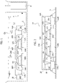
Figure 1 is exemplary of the possible application of LDS technology to manufacturing semiconductor devices, -
Figure 2 is a cross-sectional view through a semiconductor device according to embodiments of the present description, -
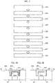
Figure 3 is a flow chart exemplary of possible steps in embodiments of the present description, -
Figures 4A and 4B schematically represent results of certain steps in the flowchart ofFigure 3 , -
Figure 5 is a schematic representation of machinery layout for implementing embodiments of the present description, and -
Figure 6 is further exemplary of possible results in a method according to embodiments of the present description. - Corresponding numerals and symbols in the different figures generally refer to corresponding parts unless otherwise indicated.
- The figures are drawn to clearly illustrate the relevant aspects of the embodiments and are not necessarily drawn to scale.
- The edges of features drawn in the figures do not necessarily indicate the termination of the extent of the feature.
- In the ensuing description, various specific details are illustrated in order to provide an in-depth understanding of various examples of embodiments according to the description. The embodiments may be obtained without one or more of the specific details, or with other methods, components, materials, etc. In other cases, known structures, materials, or operations are not illustrated or described in detail so that various aspects of the embodiments will not be obscured.
- Reference to "an embodiment" or "one embodiment" in the framework of the present description is intended to indicate that a particular configuration, structure, or characteristic described in relation to the embodiment is comprised in at least one embodiment. Hence, phrases such as "in an embodiment", "in one embodiment", or the like, that may be present in various points of the present description do not necessarily refer exactly to one and the same embodiment. Furthermore, particular configurations, structures, or characteristics may be combined in any adequate way in one or more embodiments.
- The headings/references used herein are provided merely for convenience and hence do not define the extent of protection or the scope of the embodiments.
-
Figure 1 is representative of a possible application of LDS technology in providing die-to-lead coupling in an assembly flow of plural semiconductor devices that are manufactured simultaneously and finally separated into individual devices via a singulation step. -
Figure 1 refers to a (single) device comprising a leadframe having a plurality of diepads 12A (two die pads, for instance) onto which respective semiconductor chips ordice 14 are mounted (for instance attached via die attach material 140) with an array ofleads 12B around thedie pads 12A and the semiconductor chips ordice 14. - The designation "leadframe" (or "lead frame") is currently used (see, for instance the USPC Consolidated Glossary of the United States Patent and Trademark Office) to indicate a metal frame that provides support for an integrated circuit chip or die as well as electrical leads to interconnect the integrated circuit in the die or chip to other electrical components or contacts.
- Essentially, a leadframe comprises an array of electrically-conductive formations (leads) that from an outline location extend inwardly in the direction of a semiconductor chip or die thus forming an array of electrically-conductive formations from a die pad configured to have at least one semiconductor chip or die attached thereon. This may be via conventional means such as a die attach adhesive (a die attach film or DAF, for instance).
- In
Figure 1 twodie pads 12A are illustrated having respective dice orchips 14 attached thereon ("die/dice" and "chip/chips" are used as synonyms throughout this specification). - In various embodiments,
plural chips 14 can be mounted on asingle die pad 12A: for instance, instead of being distinct elements as illustrated inFigure 1 , the twodie pads 12A may be joined to form a single die pad having two chips mounted thereon as illustrated inFigure 2 . - Laser Direct Structuring, LDS (oftentimes referred to also as direct copper interconnection or DCI technology) is a laser-based machining technique now widely used in various sectors of the industrial and consumer electronics markets, for instance for high-performance antenna integration, where an antenna design can be directly formed onto a molded plastic part. In an exemplary process, the molded parts can be produced with commercially available resins that include additives suitable for the LDS process; a broad range of resins such as polymer resins like PC, PC/ABS, ABS, LCP are currently available for that purpose.
- In LDS, a laser beam can be used to transfer a desired electrically-conductive pattern onto a plastic molding that may then be subjected to metallization (for instance via electroless and electroplating with copper or other metals) to finalize a desired conductive pattern.
- Documents such as
US 2018/342453 A1 ,US2019/115287 A1 ,US 2020/203264 A1 ,US 2020/321274 A1 ,US 2021/050226 A1 ,US 2021/050299 A1 orUS 2021/183748 A1 (all assigned to the same assignee of the present application) are exemplary of the possibility of applying LDS technology in manufacturing semiconductor devices. For instance, LDS technology facilitates replacing wires, clips or ribbons with lines/vias created by laser beam processing of LDS material followed by metallization (growing metal such as copper through plating processes, for instance). - Still referring to
Figure 1 , anencapsulation 16 of LDS material can be molded onto theleadframe - Electrically-conductive die-to-lead coupling formations can be provided (in a manner known per se: see the commonly assigned applications cited in the foregoing, for instance) in the LDS
material 16. - As illustrated in
Figure 1 , these die-to-lead coupling formations comprise: -
first vias 181 extending through the LDSencapsulation 16 between the top (front)surface 16A of the encapsulation (opposed theleadframe dice 14, -
second vias 182 extending through the LDSencapsulation 16 between the top (front)surface 16A of the encapsulation andcorresponding leads 12B in the leadframe, and - electrically-conductive lines or tracks (traces) 183 extending at the front or
top surface 16A of theencapsulation 16 and electrically coupling selected ones of thefirst vias 181 with selected ones of thesecond vias 182 to provide a desired die-to-lead electrical connection pattern between the chips ordice 14 and theleads 12B. - Providing the electrically conductive die-to-
lead formations vias 181, 182) followed by growing electrically-conductive material (a metal such as copper, for instance) at the locations activated (structured) via laser beam energy at the front ortop surface 16A of the LDSmaterial 16. - Further details on processing as discussed in the foregoing can be derived from the commonly-assigned applications referred to in the foregoing, for instance.
- Extending the use of LDS processing as discussed in the foregoing to producing die-to-die coupling formations is faced with an issue related to the very nature of these formations.
- Such die-to-die coupling formations as indicated by 200 in
Figure 1 should desirably comprise: - electrically-
conductive vias 201 extending through the LDSencapsulation 16 between the top (front)surface 16A of the encapsulation and die pads (not visible for scale reasons) at the top or front surface of the one and the other of two chips or dice 14 to be mutually connected, and - electrically-conductive lines or
tracks 202 extending bridge-like between thefirst vias 201 at the front ortop surface 16A of theencapsulation 16 to complete a desired die-to-die coupling pattern. - Laser beam structuring (also referred to as "activation") of the
vias 201 and lines ortracks 202 in the LDS material of theencapsulation 16 can be performed in the same manner of structuring thevias tracks 183 used to provide die-to-lead coupling formations as discussed previously. - A critical aspect arises in growing conductive material such as metal (via electroplating, for instance) at the structured locations to provide electrical conductivity as desired - just like in the case of the die-to-lead coupling formations.
- Growing such conductive material currently involves (in addition to electroless plating) electroplating, based on the reduction to metal material (e.g., copper) of cations of the metal to be deposited contained in an electrolyte "bath" EB.
- Cations such as Cu2+ cations are reduced to metallic copper at the cathode C by gaining electrons e from an electric current as schematically represented in
Figure 1 where A denotes the anode of the electrolyte bath containing the cations of the metal to be deposited. - For instance (as otherwise known to those of skill in the art) the electrolyte EB may contain (in the case of deposition of copper) Cu2+ cations and SO2-4 anions.
- Such a process, that is the Cu2+ cations being reduced to metallic copper at the anode in order to produce a conductive path (and, consequently, a desired growth of electrically-conductive metal such as copper at the coupling formations 200) involves gaining electrons e from an electric current flowing via the cathode C represented by the leadframe (e.g., by the
leads 12B). Such a current simply cannot flow in an arrangement as illustrated inFigure 1 : there, theformations 200 are electrically isolated from the leadframe (by the chips 14) so that Cu2+ cannot be reduced to metal (copper). - It is noted that, at least in principle, such an issue could be addressed by resorting to LDS technology - only - to provide the die-to-lead electrically
conductive formations Figure 1 . - Conventional wire bonding may represent a first candidate to consider for die-to-die coupling.
- An undesirably high resistive path and/or stress applied on device bonding parts representing (negative) factors to take into account.
- Providing the die-to-die
coupling formations 200 via a conductive paste may be another option to consider. - It is noted that filling vias structured in the
LDS material 16 with conductive paste may turn out to be unpractical due to paste viscosity. - Creating sacrificial paths within a structure as exemplified in
Figure 1 may be still another option to consider. - Again, such an approach is not exempt from drawbacks such as undesired antenna effects and possible resulting design constraints (especially in the case of devices including a high number of input/output connections).
- One or more embodiments contemplate replacing (electro)plating processes for growing metal material onto the vias and lines (tracks) structured in the
LDS material 16 with a LIFT process. - Laser-induced forward transfer (LIFT) process is a deposition process employing the transfer of material from a donor tape to acceptor substrates via a laser pulse.
- The designation LIFT applies to a process (known per se to those of skill in the art) that facilitates transfer of material from a donor tape or sheet (see 300, 302 in
Figure 5 ) to an acceptor substrate (here, the LDS material) facilitated by laser pulses. - General information on the LIFT process can be found, for instance, in P. Serra, et al.: "Laser-Induced Forward Transfer: Fundamentals and Applications", in Advanced Materials Technologies/Volume 4, Issue 1.
- Resorting to a LIFT process facilitates having increased design flexibility in a die-to-die coupling and also facilitates using copper as well as silver material for filling the vias and tracks.
-
Figure 2 (where parts or element like parts or elements already discussed in connection withFigure 1 are indicated with like reference symbols, so that a corresponding detailed description will not be repeated) is exemplary of the possibility of providing the die-to-diecoupling formations 200 using LIFT technology. - It is noted that in
Figure 2 the two semiconductor chips ordice 14 are shown mounted on asame die pad 12A as an alternative to being mounted on separate distinct die pads as illustrated inFigure 1 . - Also,
Figure 2 illustrates the possibility of molding onto the front ortop surface 16A of a "first" encapsulation of LDS material 16 a further protective encapsulation 20 (this can be non-LDS material such as a conventional epoxy resin molding compound) extending over the top portions of thevias - The flowchart of
Figure 3 is exemplary of steps that facilitate providing a semiconductor device having the structure illustrated in the cross-sectional view ofFigure 2 . - It is noted that the sequence of steps illustrated in the flowchart of
Figure 3 is merely exemplary and non-mandatory insofar as, for instance: - certain steps exemplified in
Figure 3 may be omitted and/or replaced by other steps, - additional steps (not illustrated in
Figure 3 for simplicity) may be included in the sequence, and/or - certain steps may be implemented concurrently rather than subsequently and/or in an order different from the order represented by way of example in
Figure 3 . - Also, it will be appreciated that, while possibly included in a same workstation, the LDS processing laser (to "structure" or activate the LDS material 16) and the LIFT processing laser (to transfer metal material to fill the
vias 201 and the tracks 202: see LB inFigure 5 ) will be generally different laser sources. - The
block 100 in the flowchart ofFigure 3 is exemplary of the step of providing aleadframe dice 14 thereon. - The
block 101 in the flowchart ofFigure 3 is exemplary of molding and consolidating (e.g., via thermosetting) theLDS encapsulation 16 onto theleadframe dice 14 attached thereon. - In the step of
block 102, laser beam activation energy is applied to structure in theLDS material 16 thevias 181, 182 (die-to-lead couplings) and 201 (die-to-die coupling) as well as the lines or tracks 183 (die-to-lead couplings) and 202 (die-to-die coupling or couplings: plural such couplings may in fact be provided). - The
block 103 in the flowchart ofFigure 3 is exemplary of electro-less plus electroplating metal material (copper, for instance) to complete thevias - It is otherwise noted that:
- electroless plating will form a (kind of) seed layer (see
layer 200AFigure 4A ) also on the die-to-die coupling(s) 200, that is, onto thevias 201 and the lines or tracks 202; and - electroplating as performed at the die-to-lead connections (that is, at the
vias vias 201 and the lines or tracks 202on in so far as no electrical ground connection is available at those locations. - The
block 104 in the flowchart ofFigure 3 is exemplary of the possibility of growing (filling or printing) further electrically conductive material (metal such as, e.g., copper or silver) also thevias 201 and the lines or tracks 202 via LIFT processing. - In examples as considered herein, electroplating is thus "replaced" at the
vias 201 and the lines or tracks 202 by LIFT processing for metal deposition. - It was noted that the
layer 200A formed by electroless plating (also) at thevias 201 and the lines or tracks 202 facilitates adhesion and thus robustness of the subsequent LIFT metallization. - Such a layer is indicated by 200A in both
Figures 4A and 4B . - Specifically,
Figure 4A exemplifies the action of filling thevias 201 and the line(s) 202 (with the "electroless"layer 200A formed thereon) via LIFT processing. - The
block 105 in the flow-chart ofFigure 3 is representative of in line sintering of the LIFT-printed metal material to complete thevias 201 and the line ortrack 202 in the die-to-die coupling(s) 200: seeFigure 4B . - The
block 106 in the flow-chart ofFigure 3 is representative of the second (e.g., non-LDS)encapsulation 20 being molded onto the front ortop surface 16A. - Finally, the
blocks Figure 2 ) and of singulation to produce individual semiconductor devices 10. -
Figures 4A and 4B are schematically representative of the process causing the (metal) material such as copper or silver "printed" via the LIFT process to fill thevias 201 and thetracks 202 structured at the front ortop surface 16A of the LDS material. - As visible in
Figures 4A and 4B , the metallization of the die-to-die coupling formations 200 (e.g., 201, 202) comprises a twin layer of electroless metal (see thelayer 200A) and LIFT metal. - This bi-layered structure (a first electrically
conductive material 200A electroless grown on theLDS material 16 having a second electrically conductive material transferred thereon via LIFT processing) is clearly identifiable even after sintering. - As noted, various examples may benefit from the fact that an electro-less underlayer such as 200A in
Figures 4A and 4B facilitates adhesion of the LIFT material to the (LDS) molding compound. - A similar bi-layered structure (again a first electrically conductive material electroless grown on the
LDS material 16 having a second electrically conductive material electroplated thereon as conventional in LDS processing) is likewise identifiable at the die-to-lead coupling formations - As discussed previously in connection with the
block 103 in the flow chart ofFigure 3 , electrically conductive material (e.g., copper) can be electroless grown (e.g., in a same step) both at the die-to-die coupling formations 200 (e.g., 201, 202) and at die-to-lead coupling formations - Then (further) electrically conductive material can be:
- electroplated (as conventional in LDS processing) onto the electrically conductive material electroless grown at the die-to-
lead coupling formations - LIFT-transferred onto the electrically conductive material electroless grown at the die-to-die coupling formations 200 (e.g., 201, 202) that are unsuited for conventional electroplating.
- Sintering at the die-to-die coupling formations 200 (performed as otherwise known to those of skill in the art) is advantageous in so far as it consolidates the electrically-conductive material drawn (filled) in the
vias 201 and lines or tracks 202. One or more embodiments can thus take advantage of the sintered material in providing high-conductivity electrical connections. - As discussed previously (and as otherwise conventional in the art), the LIFT process involves using a donor film (for instance a polyethylene film coated with a thin metal layer).
- Such donor film can be provided in the form of
donor tape 300 coated with the material that has to be printed (to fill thevias 201 and the lines or tracks 202, in the present case) coated thereon 302 in a roll-to-roll coating process (between two rolls R1, R2). This offers the advantage of facilitating possible handling of plural materials at the same time). The thickness of thecoating 302 determines the height of the final layer. - Laser beam energy as exemplified at LB in
Figure 5 then be applied to thecoated donor tape 300, 302 (from the uncoated side) at those locations (generically indicated with 304 inFigure 5 ) where electrically conductive material such as copper or silver is to be transferred onto theLDS material 16 to fill metal into thevias 201 and over the lines or tracks 202 previously structured therein via laser beam structuring (activation). -
Figure 6 is exemplary of the fact that transfer of the filling material from the donor tape of the LIFT process may also involve forming at the front or top surface of thedice 14upstanding formations 400 having a thickness leading the distal (upper) end of this material to be visible at the surface of theLDS material 16. Those upstanding formations can be used as references (fiducials) in LDS processing as disclosed inItalian patent application 102021000014198 - Without prejudice to the underlying principles, the details and the embodiments may vary, even significantly, with respect to what has been described by way of example only without departing from the scope of the embodiments.
- The extent of protection is determined by the annexed claims.
Claims (5)
- A method, comprising:arranging on a substrate (12A, 12B) at least one pair of semiconductor dice (14) comprising a first semiconductor die and a second semiconductor die,molding an encapsulation (16) of laser direct structuring, LDS material onto the first semiconductor die and the second semiconductor die arranged on the substrate (12A, 12B), the encapsulation of LDS material (16) having a surface (16A) opposite the substrate (12A, 12B),providing at least one electrically conductive die-to-die coupling formation (200) between the first semiconductor die and the second semiconductor die, the at least one die-to-die coupling formation (200) comprising die vias (201) extending through the LDS material between the surface (16A) of the encapsulation of LDS material (16) opposite the substrate (12A, 12B) and the one and the other (14) of the first semiconductor die and the second semiconductor die as well as a die-to-die line (202) extending at the surface (16A) of the encapsulation of LDS material (16) opposite the substrate (12A, 12B) and coupling said die vias (201),wherein providing said at least one electrically conductive die-to-die coupling formation (200) comprises:applying laser beam energy (LB) to selected locations of the surface (16A) of the encapsulation of LDS material (16) opposite the substrate (12A, 12B) to laser-activate the LDS material (16) and structure therein said die vias (201) as well as said die-to-die line (202),electroless growing electrically conductive material (200A) onto said die vias (201) as well as said die-to-die line (202) structured via laser beam energy (LB) in the encapsulation of LDS material (16), andapplying laser-induced forward transfer, LIFT processing to transfer electrically conductive material onto the electrically conductive material (200A) electroless grown onto said die vias (201) and said die-to-die line (202).
- The method of claim 1, comprising sintering (105) said electrically conductive material transferred via LIFT processing onto said die vias (201) and said die-to-die line (202) extending between the die vias (201).
- The method of claim 1 or claim 2, comprising applying LIFT processing to said die vias (201) and said die-to-die line (202) extending between the die vias (201) to transfer metal material, preferably copper or silver, onto said die vias (201) and said die-to-die line (202) extending between the die vias (201).
- The method of any of the previous claims, comprising:arranging said at least one pair of semiconductor dice (14) on at least one die pad (12A) in said substrate (12A, 12B), the substrate comprising an array of electrically conductive leads (12B) around said at least one die pad (12A), andapplying LDS processing to said encapsulation (16) of LDS material to provide die-to-lead electrically conductive formations (181, 182, 183) coupling said first and second semiconductor dice (14) with selected ones of said electrically conductive leads (12B) in said array of electrically conductive leads (12B), wherein said die-to-lead electrically conductive formations (181, 182, 183) comprise:first vias (181) extending through the LDS material between the surface (16A) of the encapsulation of LDS material (16) opposite the substrate (12A, 12B) and the one and the other of the first semiconductor die and the second semiconductor die (14),second vias (182) extending through the LDS material between the surface (16A) of the encapsulation of LDS material (16) opposite the substrate (12A, 12B) and selected ones of the electrically conductive leads in said array of electrically conductive leads (12B), andelectrically conductive lines (183) extending at the surface (16A) of the encapsulation of LDS material (16) opposite the substrate (12A, 12B) between selected ones of said first vias (181) and selected ones of said second vias (182).
- The method of claim 4, comprising:at said first vias (181), said second vias (182), and said electrically conductive lines (183) in said die-to-lead electrically conductive formations (181, 182, 183), electroless growing electrically conductive material on said LDS material (16) followed by electroplating electrically conductive material onto the electroless grown electrically conductive material, andat said die vias (201) as well as said die-to-die line (202) in said at least one electrically conductive die-to-die coupling formation (200), electroless growing electrically conductive material (200A) on said LDS material (16) followed by transferring via LIFT processing electrically conductive material onto the electroless grown electrically conductive material (200A).
Applications Claiming Priority (1)
| Application Number | Priority Date | Filing Date | Title |
|---|---|---|---|
| IT202100020540 | 2021-07-30 |
Publications (2)
| Publication Number | Publication Date |
|---|---|
| EP4125119A1 true EP4125119A1 (en) | 2023-02-01 |
| EP4125119B1 EP4125119B1 (en) | 2024-04-17 |
Family
ID=78049705
Family Applications (1)
| Application Number | Title | Priority Date | Filing Date |
|---|---|---|---|
| EP22187481.1A Active EP4125119B1 (en) | 2021-07-30 | 2022-07-28 | Method of coupling semiconductor dice |
Country Status (2)
| Country | Link |
|---|---|
| US (1) | US12525512B2 (en) |
| EP (1) | EP4125119B1 (en) |
Cited By (1)
| Publication number | Priority date | Publication date | Assignee | Title |
|---|---|---|---|---|
| US20230035445A1 (en) * | 2021-07-30 | 2023-02-02 | Stmicroelectronics S.R.L. | Method of coupling semiconductor dice, tool for use therein and corresponding semiconductor device |
Families Citing this family (5)
| Publication number | Priority date | Publication date | Assignee | Title |
|---|---|---|---|---|
| IT202100022607A1 (en) | 2021-08-31 | 2023-03-03 | St Microelectronics Srl | Process for manufacturing semiconductor devices and corresponding semiconductor device |
| IT202300017841A1 (en) * | 2023-08-30 | 2025-03-02 | St Microelectronics Int Nv | PROCEDURE FOR MANUFACTURING SEMICONDUCTOR DEVICES AND CORRESPONDING SEMICONDUCTOR DEVICE |
| IT202300020505A1 (en) | 2023-10-04 | 2025-04-04 | St Microelectronics Int Nv | PROCEDURE FOR MANUFACTURING SEMICONDUCTOR DEVICES AND CORRESPONDING DEVICE |
| IT202400004246A1 (en) | 2024-02-28 | 2025-08-28 | St Microelectronics Int Nv | PROCEDURE FOR MANUFACTURING SEMICONDUCTOR DEVICES AND CORRESPONDING DEVICE |
| IT202400004300A1 (en) | 2024-02-28 | 2025-08-28 | St Microelectronics Int Nv | PROCEDURE FOR MANUFACTURING SEMICONDUCTOR DEVICES AND CORRESPONDING SEMICONDUCTOR DEVICE |
Citations (10)
| Publication number | Priority date | Publication date | Assignee | Title |
|---|---|---|---|---|
| US20090072379A1 (en) | 2007-09-14 | 2009-03-19 | Infineon Technologies Ag | Semiconductor device |
| US20110003440A1 (en) | 2009-03-31 | 2011-01-06 | Infineon Technologies Ag | Method of manufacturing a semiconductor device |
| US20180342453A1 (en) | 2017-05-23 | 2018-11-29 | Stmicroelectronics S.R.L. | Method of manufacturing semiconductor devices and corresponding product |
| US20190115287A1 (en) | 2017-10-12 | 2019-04-18 | Stmicroelectronics S.R.L. | Method of manufacturing semiconductor devices, corresponding device and circuit |
| US20200203264A1 (en) | 2018-12-24 | 2020-06-25 | Stmicroelectronics S.R.L. | Method of manufacturing semiconductor devices and corresponding semiconductor device |
| US20200321269A1 (en) | 2019-04-04 | 2020-10-08 | Infineon Technologies Ag | Chip to Lead Interconnect in Encapsulant of Molded Semiconductor Package |
| US20200321274A1 (en) | 2019-04-05 | 2020-10-08 | Stmicroelectronics S.R.L. | Method of manufacturing leadframes for semiconductor devices, corresponding leadframe and semicondctor device |
| US20210050299A1 (en) | 2019-08-16 | 2021-02-18 | Stmicroelectronics S.R.L. | Method of manufacturing semiconductor devices and corresponding semiconductor device |
| US20210050226A1 (en) | 2019-08-16 | 2021-02-18 | Stmicroelectronics S.R.L. | Method of manufacturing semiconductor devices and corresponding semiconductor device |
| US20210183748A1 (en) | 2019-12-17 | 2021-06-17 | Stmicroelectronics S.R.L. | Method of manufacturing semiconductor devices and corresponding semiconductor device |
Family Cites Families (7)
| Publication number | Priority date | Publication date | Assignee | Title |
|---|---|---|---|---|
| US8338936B2 (en) | 2008-07-24 | 2012-12-25 | Infineon Technologies Ag | Semiconductor device and manufacturing method |
| US8970046B2 (en) * | 2011-07-18 | 2015-03-03 | Samsung Electronics Co., Ltd. | Semiconductor packages and methods of forming the same |
| US9761534B2 (en) * | 2015-09-21 | 2017-09-12 | Mediatek Inc. | Semiconductor package, semiconductor device using the same and manufacturing method thereof |
| US10211161B2 (en) * | 2016-08-31 | 2019-02-19 | Advanced Semiconductor Engineering, Inc. | Semiconductor package structure having a protection layer |
| KR102600623B1 (en) | 2017-02-08 | 2023-11-08 | 삼성전자주식회사 | Probe card assembly |
| IT201900022632A1 (en) | 2019-12-02 | 2021-06-02 | St Microelectronics Srl | PROCEDURE FOR MANUFACTURING SEMICONDUCTOR DEVICES AND CORRESPONDING SEMICONDUCTOR DEVICE |
| CN218333795U (en) | 2021-07-30 | 2023-01-17 | 意法半导体股份有限公司 | Semiconductor device with a plurality of transistors |
-
2022
- 2022-07-25 US US17/872,774 patent/US12525512B2/en active Active
- 2022-07-28 EP EP22187481.1A patent/EP4125119B1/en active Active
Patent Citations (10)
| Publication number | Priority date | Publication date | Assignee | Title |
|---|---|---|---|---|
| US20090072379A1 (en) | 2007-09-14 | 2009-03-19 | Infineon Technologies Ag | Semiconductor device |
| US20110003440A1 (en) | 2009-03-31 | 2011-01-06 | Infineon Technologies Ag | Method of manufacturing a semiconductor device |
| US20180342453A1 (en) | 2017-05-23 | 2018-11-29 | Stmicroelectronics S.R.L. | Method of manufacturing semiconductor devices and corresponding product |
| US20190115287A1 (en) | 2017-10-12 | 2019-04-18 | Stmicroelectronics S.R.L. | Method of manufacturing semiconductor devices, corresponding device and circuit |
| US20200203264A1 (en) | 2018-12-24 | 2020-06-25 | Stmicroelectronics S.R.L. | Method of manufacturing semiconductor devices and corresponding semiconductor device |
| US20200321269A1 (en) | 2019-04-04 | 2020-10-08 | Infineon Technologies Ag | Chip to Lead Interconnect in Encapsulant of Molded Semiconductor Package |
| US20200321274A1 (en) | 2019-04-05 | 2020-10-08 | Stmicroelectronics S.R.L. | Method of manufacturing leadframes for semiconductor devices, corresponding leadframe and semicondctor device |
| US20210050299A1 (en) | 2019-08-16 | 2021-02-18 | Stmicroelectronics S.R.L. | Method of manufacturing semiconductor devices and corresponding semiconductor device |
| US20210050226A1 (en) | 2019-08-16 | 2021-02-18 | Stmicroelectronics S.R.L. | Method of manufacturing semiconductor devices and corresponding semiconductor device |
| US20210183748A1 (en) | 2019-12-17 | 2021-06-17 | Stmicroelectronics S.R.L. | Method of manufacturing semiconductor devices and corresponding semiconductor device |
Non-Patent Citations (1)
| Title |
|---|
| P. SERRA ET AL.: "Laser-Induced Forward Transfer: Fundamentals and Applications", ADVANCED MATERIALS TECHNOLOGIES, vol. 4 |
Cited By (2)
| Publication number | Priority date | Publication date | Assignee | Title |
|---|---|---|---|---|
| US20230035445A1 (en) * | 2021-07-30 | 2023-02-02 | Stmicroelectronics S.R.L. | Method of coupling semiconductor dice, tool for use therein and corresponding semiconductor device |
| US12500148B2 (en) * | 2021-07-30 | 2025-12-16 | Stmicroelectronics S.R.L. | Method of coupling semiconductor dice, tool for use therein and corresponding semiconductor device |
Also Published As
| Publication number | Publication date |
|---|---|
| US20230035470A1 (en) | 2023-02-02 |
| EP4125119B1 (en) | 2024-04-17 |
| US12525512B2 (en) | 2026-01-13 |
Similar Documents
| Publication | Publication Date | Title |
|---|---|---|
| EP4125119B1 (en) | Method of coupling semiconductor dice | |
| US12500148B2 (en) | Method of coupling semiconductor dice, tool for use therein and corresponding semiconductor device | |
| CN218333795U (en) | Semiconductor device with a plurality of transistors | |
| US10777478B2 (en) | Semiconductor package device for power device | |
| US11626379B2 (en) | Method of manufacturing semiconductor devices and corresponding semiconductor device | |
| EP4181177B1 (en) | Method of manufacturing semiconductor devices and corresponding semiconductor device | |
| EP4099368A1 (en) | Method of manufacturing semiconductor devices and corresponding semiconductor device | |
| US20250015038A1 (en) | Method of manufacturing semiconductor devices and corresponding semiconductor device | |
| US20250273481A1 (en) | Method of manufacturing semiconductor devices and corresponding device | |
| CN106684051A (en) | Metal post conducting chip-scale packaging structure and technique thereof | |
| US20230245944A1 (en) | Fan-out type package preparation method of fan-out type package | |
| CN220510010U (en) | Semiconductor device with a semiconductor layer having a plurality of semiconductor layers | |
| US20230230948A1 (en) | Method of manufacturing semiconductor devices and corresponding semiconductor device | |
| US20230360928A1 (en) | Method for manufacturing semiconductor devices and corresponding semiconductor device | |
| US12354886B2 (en) | Method of manufacturing semiconductor devices and corresponding semiconductor device | |
| EP4273923B1 (en) | Method of manufacturing semiconductor devices and corresponding semiconductor device | |
| CN117012651A (en) | Method for manufacturing semiconductor device and corresponding semiconductor device | |
| CN117012652B (en) | Method for manufacturing semiconductor device and corresponding semiconductor device | |
| US20240145429A1 (en) | Method of manufacturing semiconductor devices, corresponding leadframe, mold and semiconductor device | |
| US20250273623A1 (en) | Method of manufacturing semiconductor devices and corresponding device | |
| US12412796B2 (en) | Method of manufacturing semiconductor devices and corresponding semiconductor device | |
| CN222953081U (en) | Semiconductor device with a semiconductor layer having a plurality of semiconductor layers | |
| US20250372488A1 (en) | Method of manufacturing semiconductor devices and corresponding semiconductor device | |
| EP4276889A1 (en) | Method of manufacturing a semiconductor device and the corresponding semiconductor device | |
| US20230386980A1 (en) | Method of manufacturing semiconductor devices and corresponding semiconductor device |
Legal Events
| Date | Code | Title | Description |
|---|---|---|---|
| PUAI | Public reference made under article 153(3) epc to a published international application that has entered the european phase |
Free format text: ORIGINAL CODE: 0009012 |
|
| STAA | Information on the status of an ep patent application or granted ep patent |
Free format text: STATUS: THE APPLICATION HAS BEEN PUBLISHED |
|
| AK | Designated contracting states |
Kind code of ref document: A1 Designated state(s): AL AT BE BG CH CY CZ DE DK EE ES FI FR GB GR HR HU IE IS IT LI LT LU LV MC MK MT NL NO PL PT RO RS SE SI SK SM TR |
|
| STAA | Information on the status of an ep patent application or granted ep patent |
Free format text: STATUS: REQUEST FOR EXAMINATION WAS MADE |
|
| 17P | Request for examination filed |
Effective date: 20230710 |
|
| RBV | Designated contracting states (corrected) |
Designated state(s): AL AT BE BG CH CY CZ DE DK EE ES FI FR GB GR HR HU IE IS IT LI LT LU LV MC MK MT NL NO PL PT RO RS SE SI SK SM TR |
|
| GRAP | Despatch of communication of intention to grant a patent |
Free format text: ORIGINAL CODE: EPIDOSNIGR1 |
|
| STAA | Information on the status of an ep patent application or granted ep patent |
Free format text: STATUS: GRANT OF PATENT IS INTENDED |
|
| RIC1 | Information provided on ipc code assigned before grant |
Ipc: H01L 25/07 20060101ALN20231201BHEP Ipc: H01L 25/16 20230101ALN20231201BHEP Ipc: H01L 25/00 20060101ALI20231201BHEP Ipc: H01L 23/29 20060101ALI20231201BHEP Ipc: H01L 23/31 20060101ALI20231201BHEP Ipc: H01L 23/495 20060101ALI20231201BHEP Ipc: H01L 21/285 20060101ALI20231201BHEP Ipc: H01L 21/02 20060101ALI20231201BHEP Ipc: C23C 14/28 20060101ALI20231201BHEP Ipc: C23C 14/04 20060101ALI20231201BHEP Ipc: H01L 21/60 20060101ALI20231201BHEP Ipc: H01L 21/48 20060101ALI20231201BHEP Ipc: H01L 21/56 20060101ALI20231201BHEP Ipc: H01L 25/065 20230101ALI20231201BHEP Ipc: H01L 23/00 20060101AFI20231201BHEP |
|
| INTG | Intention to grant announced |
Effective date: 20231222 |
|
| RIC1 | Information provided on ipc code assigned before grant |
Ipc: H01L 25/07 20060101ALN20231212BHEP Ipc: H01L 25/16 20230101ALN20231212BHEP Ipc: H01L 25/00 20060101ALI20231212BHEP Ipc: H01L 23/29 20060101ALI20231212BHEP Ipc: H01L 23/31 20060101ALI20231212BHEP Ipc: H01L 23/495 20060101ALI20231212BHEP Ipc: H01L 21/285 20060101ALI20231212BHEP Ipc: H01L 21/02 20060101ALI20231212BHEP Ipc: C23C 14/28 20060101ALI20231212BHEP Ipc: C23C 14/04 20060101ALI20231212BHEP Ipc: H01L 21/60 20060101ALI20231212BHEP Ipc: H01L 21/48 20060101ALI20231212BHEP Ipc: H01L 21/56 20060101ALI20231212BHEP Ipc: H01L 25/065 20230101ALI20231212BHEP Ipc: H01L 23/00 20060101AFI20231212BHEP |
|
| GRAS | Grant fee paid |
Free format text: ORIGINAL CODE: EPIDOSNIGR3 |
|
| GRAA | (expected) grant |
Free format text: ORIGINAL CODE: 0009210 |
|
| STAA | Information on the status of an ep patent application or granted ep patent |
Free format text: STATUS: THE PATENT HAS BEEN GRANTED |
|
| AK | Designated contracting states |
Kind code of ref document: B1 Designated state(s): AL AT BE BG CH CY CZ DE DK EE ES FI FR GB GR HR HU IE IS IT LI LT LU LV MC MK MT NL NO PL PT RO RS SE SI SK SM TR |
|
| REG | Reference to a national code |
Ref country code: GB Ref legal event code: FG4D |
|
| REG | Reference to a national code |
Ref country code: CH Ref legal event code: EP |
|
| REG | Reference to a national code |
Ref country code: DE Ref legal event code: R096 Ref document number: 602022002897 Country of ref document: DE |
|
| REG | Reference to a national code |
Ref country code: IE Ref legal event code: FG4D |
|
| REG | Reference to a national code |
Ref country code: LT Ref legal event code: MG9D |
|
| REG | Reference to a national code |
Ref country code: NL Ref legal event code: MP Effective date: 20240417 |
|
| REG | Reference to a national code |
Ref country code: AT Ref legal event code: MK05 Ref document number: 1678109 Country of ref document: AT Kind code of ref document: T Effective date: 20240417 |
|
| PG25 | Lapsed in a contracting state [announced via postgrant information from national office to epo] |
Ref country code: NL Free format text: LAPSE BECAUSE OF FAILURE TO SUBMIT A TRANSLATION OF THE DESCRIPTION OR TO PAY THE FEE WITHIN THE PRESCRIBED TIME-LIMIT Effective date: 20240417 |
|
| PG25 | Lapsed in a contracting state [announced via postgrant information from national office to epo] |
Ref country code: NL Free format text: LAPSE BECAUSE OF FAILURE TO SUBMIT A TRANSLATION OF THE DESCRIPTION OR TO PAY THE FEE WITHIN THE PRESCRIBED TIME-LIMIT Effective date: 20240417 |
|
| PG25 | Lapsed in a contracting state [announced via postgrant information from national office to epo] |
Ref country code: IS Free format text: LAPSE BECAUSE OF FAILURE TO SUBMIT A TRANSLATION OF THE DESCRIPTION OR TO PAY THE FEE WITHIN THE PRESCRIBED TIME-LIMIT Effective date: 20240817 |
|
| PG25 | Lapsed in a contracting state [announced via postgrant information from national office to epo] |
Ref country code: BG Free format text: LAPSE BECAUSE OF FAILURE TO SUBMIT A TRANSLATION OF THE DESCRIPTION OR TO PAY THE FEE WITHIN THE PRESCRIBED TIME-LIMIT Effective date: 20240417 |
|
| PG25 | Lapsed in a contracting state [announced via postgrant information from national office to epo] |
Ref country code: HR Free format text: LAPSE BECAUSE OF FAILURE TO SUBMIT A TRANSLATION OF THE DESCRIPTION OR TO PAY THE FEE WITHIN THE PRESCRIBED TIME-LIMIT Effective date: 20240417 Ref country code: FI Free format text: LAPSE BECAUSE OF FAILURE TO SUBMIT A TRANSLATION OF THE DESCRIPTION OR TO PAY THE FEE WITHIN THE PRESCRIBED TIME-LIMIT Effective date: 20240417 |
|
| PG25 | Lapsed in a contracting state [announced via postgrant information from national office to epo] |
Ref country code: GR Free format text: LAPSE BECAUSE OF FAILURE TO SUBMIT A TRANSLATION OF THE DESCRIPTION OR TO PAY THE FEE WITHIN THE PRESCRIBED TIME-LIMIT Effective date: 20240718 |
|
| PG25 | Lapsed in a contracting state [announced via postgrant information from national office to epo] |
Ref country code: PT Free format text: LAPSE BECAUSE OF FAILURE TO SUBMIT A TRANSLATION OF THE DESCRIPTION OR TO PAY THE FEE WITHIN THE PRESCRIBED TIME-LIMIT Effective date: 20240819 |
|
| PG25 | Lapsed in a contracting state [announced via postgrant information from national office to epo] |
Ref country code: ES Free format text: LAPSE BECAUSE OF FAILURE TO SUBMIT A TRANSLATION OF THE DESCRIPTION OR TO PAY THE FEE WITHIN THE PRESCRIBED TIME-LIMIT Effective date: 20240417 |
|
| PG25 | Lapsed in a contracting state [announced via postgrant information from national office to epo] |
Ref country code: AT Free format text: LAPSE BECAUSE OF FAILURE TO SUBMIT A TRANSLATION OF THE DESCRIPTION OR TO PAY THE FEE WITHIN THE PRESCRIBED TIME-LIMIT Effective date: 20240417 |
|
| PG25 | Lapsed in a contracting state [announced via postgrant information from national office to epo] |
Ref country code: PL Free format text: LAPSE BECAUSE OF FAILURE TO SUBMIT A TRANSLATION OF THE DESCRIPTION OR TO PAY THE FEE WITHIN THE PRESCRIBED TIME-LIMIT Effective date: 20240417 |
|
| PG25 | Lapsed in a contracting state [announced via postgrant information from national office to epo] |
Ref country code: LV Free format text: LAPSE BECAUSE OF FAILURE TO SUBMIT A TRANSLATION OF THE DESCRIPTION OR TO PAY THE FEE WITHIN THE PRESCRIBED TIME-LIMIT Effective date: 20240417 |
|
| PG25 | Lapsed in a contracting state [announced via postgrant information from national office to epo] |
Ref country code: PT Free format text: LAPSE BECAUSE OF FAILURE TO SUBMIT A TRANSLATION OF THE DESCRIPTION OR TO PAY THE FEE WITHIN THE PRESCRIBED TIME-LIMIT Effective date: 20240819 Ref country code: PL Free format text: LAPSE BECAUSE OF FAILURE TO SUBMIT A TRANSLATION OF THE DESCRIPTION OR TO PAY THE FEE WITHIN THE PRESCRIBED TIME-LIMIT Effective date: 20240417 Ref country code: NO Free format text: LAPSE BECAUSE OF FAILURE TO SUBMIT A TRANSLATION OF THE DESCRIPTION OR TO PAY THE FEE WITHIN THE PRESCRIBED TIME-LIMIT Effective date: 20240717 Ref country code: LV Free format text: LAPSE BECAUSE OF FAILURE TO SUBMIT A TRANSLATION OF THE DESCRIPTION OR TO PAY THE FEE WITHIN THE PRESCRIBED TIME-LIMIT Effective date: 20240417 Ref country code: IS Free format text: LAPSE BECAUSE OF FAILURE TO SUBMIT A TRANSLATION OF THE DESCRIPTION OR TO PAY THE FEE WITHIN THE PRESCRIBED TIME-LIMIT Effective date: 20240817 Ref country code: HR Free format text: LAPSE BECAUSE OF FAILURE TO SUBMIT A TRANSLATION OF THE DESCRIPTION OR TO PAY THE FEE WITHIN THE PRESCRIBED TIME-LIMIT Effective date: 20240417 Ref country code: GR Free format text: LAPSE BECAUSE OF FAILURE TO SUBMIT A TRANSLATION OF THE DESCRIPTION OR TO PAY THE FEE WITHIN THE PRESCRIBED TIME-LIMIT Effective date: 20240718 Ref country code: FI Free format text: LAPSE BECAUSE OF FAILURE TO SUBMIT A TRANSLATION OF THE DESCRIPTION OR TO PAY THE FEE WITHIN THE PRESCRIBED TIME-LIMIT Effective date: 20240417 Ref country code: ES Free format text: LAPSE BECAUSE OF FAILURE TO SUBMIT A TRANSLATION OF THE DESCRIPTION OR TO PAY THE FEE WITHIN THE PRESCRIBED TIME-LIMIT Effective date: 20240417 Ref country code: BG Free format text: LAPSE BECAUSE OF FAILURE TO SUBMIT A TRANSLATION OF THE DESCRIPTION OR TO PAY THE FEE WITHIN THE PRESCRIBED TIME-LIMIT Effective date: 20240417 Ref country code: AT Free format text: LAPSE BECAUSE OF FAILURE TO SUBMIT A TRANSLATION OF THE DESCRIPTION OR TO PAY THE FEE WITHIN THE PRESCRIBED TIME-LIMIT Effective date: 20240417 Ref country code: RS Free format text: LAPSE BECAUSE OF FAILURE TO SUBMIT A TRANSLATION OF THE DESCRIPTION OR TO PAY THE FEE WITHIN THE PRESCRIBED TIME-LIMIT Effective date: 20240717 |
|
| PG25 | Lapsed in a contracting state [announced via postgrant information from national office to epo] |
Ref country code: DK Free format text: LAPSE BECAUSE OF FAILURE TO SUBMIT A TRANSLATION OF THE DESCRIPTION OR TO PAY THE FEE WITHIN THE PRESCRIBED TIME-LIMIT Effective date: 20240417 |
|
| REG | Reference to a national code |
Ref country code: DE Ref legal event code: R097 Ref document number: 602022002897 Country of ref document: DE |
|
| PG25 | Lapsed in a contracting state [announced via postgrant information from national office to epo] |
Ref country code: EE Free format text: LAPSE BECAUSE OF FAILURE TO SUBMIT A TRANSLATION OF THE DESCRIPTION OR TO PAY THE FEE WITHIN THE PRESCRIBED TIME-LIMIT Effective date: 20240417 |
|
| PG25 | Lapsed in a contracting state [announced via postgrant information from national office to epo] |
Ref country code: CZ Free format text: LAPSE BECAUSE OF FAILURE TO SUBMIT A TRANSLATION OF THE DESCRIPTION OR TO PAY THE FEE WITHIN THE PRESCRIBED TIME-LIMIT Effective date: 20240417 |
|
| PG25 | Lapsed in a contracting state [announced via postgrant information from national office to epo] |
Ref country code: SK Free format text: LAPSE BECAUSE OF FAILURE TO SUBMIT A TRANSLATION OF THE DESCRIPTION OR TO PAY THE FEE WITHIN THE PRESCRIBED TIME-LIMIT Effective date: 20240417 Ref country code: RO Free format text: LAPSE BECAUSE OF FAILURE TO SUBMIT A TRANSLATION OF THE DESCRIPTION OR TO PAY THE FEE WITHIN THE PRESCRIBED TIME-LIMIT Effective date: 20240417 |
|
| PG25 | Lapsed in a contracting state [announced via postgrant information from national office to epo] |
Ref country code: SM Free format text: LAPSE BECAUSE OF FAILURE TO SUBMIT A TRANSLATION OF THE DESCRIPTION OR TO PAY THE FEE WITHIN THE PRESCRIBED TIME-LIMIT Effective date: 20240417 |
|
| PG25 | Lapsed in a contracting state [announced via postgrant information from national office to epo] |
Ref country code: SM Free format text: LAPSE BECAUSE OF FAILURE TO SUBMIT A TRANSLATION OF THE DESCRIPTION OR TO PAY THE FEE WITHIN THE PRESCRIBED TIME-LIMIT Effective date: 20240417 Ref country code: SK Free format text: LAPSE BECAUSE OF FAILURE TO SUBMIT A TRANSLATION OF THE DESCRIPTION OR TO PAY THE FEE WITHIN THE PRESCRIBED TIME-LIMIT Effective date: 20240417 Ref country code: RO Free format text: LAPSE BECAUSE OF FAILURE TO SUBMIT A TRANSLATION OF THE DESCRIPTION OR TO PAY THE FEE WITHIN THE PRESCRIBED TIME-LIMIT Effective date: 20240417 Ref country code: EE Free format text: LAPSE BECAUSE OF FAILURE TO SUBMIT A TRANSLATION OF THE DESCRIPTION OR TO PAY THE FEE WITHIN THE PRESCRIBED TIME-LIMIT Effective date: 20240417 Ref country code: DK Free format text: LAPSE BECAUSE OF FAILURE TO SUBMIT A TRANSLATION OF THE DESCRIPTION OR TO PAY THE FEE WITHIN THE PRESCRIBED TIME-LIMIT Effective date: 20240417 Ref country code: CZ Free format text: LAPSE BECAUSE OF FAILURE TO SUBMIT A TRANSLATION OF THE DESCRIPTION OR TO PAY THE FEE WITHIN THE PRESCRIBED TIME-LIMIT Effective date: 20240417 |
|
| PG25 | Lapsed in a contracting state [announced via postgrant information from national office to epo] |
Ref country code: IT Free format text: LAPSE BECAUSE OF FAILURE TO SUBMIT A TRANSLATION OF THE DESCRIPTION OR TO PAY THE FEE WITHIN THE PRESCRIBED TIME-LIMIT Effective date: 20240417 Ref country code: MC Free format text: LAPSE BECAUSE OF FAILURE TO SUBMIT A TRANSLATION OF THE DESCRIPTION OR TO PAY THE FEE WITHIN THE PRESCRIBED TIME-LIMIT Effective date: 20240417 |
|
| PLBE | No opposition filed within time limit |
Free format text: ORIGINAL CODE: 0009261 |
|
| STAA | Information on the status of an ep patent application or granted ep patent |
Free format text: STATUS: NO OPPOSITION FILED WITHIN TIME LIMIT |
|
| PG25 | Lapsed in a contracting state [announced via postgrant information from national office to epo] |
Ref country code: LU Free format text: LAPSE BECAUSE OF NON-PAYMENT OF DUE FEES Effective date: 20240728 |
|
| 26N | No opposition filed |
Effective date: 20250120 |
|
| PG25 | Lapsed in a contracting state [announced via postgrant information from national office to epo] |
Ref country code: LU Free format text: LAPSE BECAUSE OF NON-PAYMENT OF DUE FEES Effective date: 20240728 |
|
| PG25 | Lapsed in a contracting state [announced via postgrant information from national office to epo] |
Ref country code: SI Free format text: LAPSE BECAUSE OF FAILURE TO SUBMIT A TRANSLATION OF THE DESCRIPTION OR TO PAY THE FEE WITHIN THE PRESCRIBED TIME-LIMIT Effective date: 20240417 Ref country code: BE Free format text: LAPSE BECAUSE OF NON-PAYMENT OF DUE FEES Effective date: 20240731 |
|
| PG25 | Lapsed in a contracting state [announced via postgrant information from national office to epo] |
Ref country code: FR Free format text: LAPSE BECAUSE OF NON-PAYMENT OF DUE FEES Effective date: 20240731 |
|
| REG | Reference to a national code |
Ref country code: BE Ref legal event code: MM Effective date: 20240731 |
|
| PG25 | Lapsed in a contracting state [announced via postgrant information from national office to epo] |
Ref country code: IE Free format text: LAPSE BECAUSE OF NON-PAYMENT OF DUE FEES Effective date: 20240728 |
|
| PG25 | Lapsed in a contracting state [announced via postgrant information from national office to epo] |
Ref country code: SE Free format text: LAPSE BECAUSE OF FAILURE TO SUBMIT A TRANSLATION OF THE DESCRIPTION OR TO PAY THE FEE WITHIN THE PRESCRIBED TIME-LIMIT Effective date: 20240417 |
|
| PGFP | Annual fee paid to national office [announced via postgrant information from national office to epo] |
Ref country code: DE Payment date: 20250620 Year of fee payment: 4 |
|
| REG | Reference to a national code |
Ref country code: DE Ref legal event code: R079 Ref document number: 602022002897 Country of ref document: DE Free format text: PREVIOUS MAIN CLASS: H01L0023000000 Ipc: H10W0099000000 |
|
| PG25 | Lapsed in a contracting state [announced via postgrant information from national office to epo] |
Ref country code: CY Free format text: LAPSE BECAUSE OF FAILURE TO SUBMIT A TRANSLATION OF THE DESCRIPTION OR TO PAY THE FEE WITHIN THE PRESCRIBED TIME-LIMIT; INVALID AB INITIO Effective date: 20220728 |
|
| REG | Reference to a national code |
Ref country code: CH Ref legal event code: H13 Free format text: ST27 STATUS EVENT CODE: U-0-0-H10-H13 (AS PROVIDED BY THE NATIONAL OFFICE) Effective date: 20260224 |
|
| PG25 | Lapsed in a contracting state [announced via postgrant information from national office to epo] |
Ref country code: HU Free format text: LAPSE BECAUSE OF FAILURE TO SUBMIT A TRANSLATION OF THE DESCRIPTION OR TO PAY THE FEE WITHIN THE PRESCRIBED TIME-LIMIT; INVALID AB INITIO Effective date: 20220728 |
|
| PG25 | Lapsed in a contracting state [announced via postgrant information from national office to epo] |
Ref country code: CH Free format text: LAPSE BECAUSE OF NON-PAYMENT OF DUE FEES Effective date: 20250731 |