EP4124964A1 - Verfahren und vorrichtung zur hochleistungshandhabung von seitenfehlern für mandantenfähige skalierbare beschleuniger - Google Patents
Verfahren und vorrichtung zur hochleistungshandhabung von seitenfehlern für mandantenfähige skalierbare beschleuniger Download PDFInfo
- Publication number
- EP4124964A1 EP4124964A1 EP22181043.5A EP22181043A EP4124964A1 EP 4124964 A1 EP4124964 A1 EP 4124964A1 EP 22181043 A EP22181043 A EP 22181043A EP 4124964 A1 EP4124964 A1 EP 4124964A1
- Authority
- EP
- European Patent Office
- Prior art keywords
- work
- page fault
- page
- fault
- descriptor
- Prior art date
- Legal status (The legal status is an assumption and is not a legal conclusion. Google has not performed a legal analysis and makes no representation as to the accuracy of the status listed.)
- Granted
Links
Images


Classifications
-
- G—PHYSICS
- G06—COMPUTING OR CALCULATING; COUNTING
- G06F—ELECTRIC DIGITAL DATA PROCESSING
- G06F12/00—Accessing, addressing or allocating within memory systems or architectures
- G06F12/02—Addressing or allocation; Relocation
- G06F12/08—Addressing or allocation; Relocation in hierarchically structured memory systems, e.g. virtual memory systems
- G06F12/10—Address translation
-
- G—PHYSICS
- G06—COMPUTING OR CALCULATING; COUNTING
- G06F—ELECTRIC DIGITAL DATA PROCESSING
- G06F11/00—Error detection; Error correction; Monitoring
- G06F11/07—Responding to the occurrence of a fault, e.g. fault tolerance
- G06F11/0703—Error or fault processing not based on redundancy, i.e. by taking additional measures to deal with the error or fault not making use of redundancy in operation, in hardware, or in data representation
- G06F11/079—Root cause analysis, i.e. error or fault diagnosis
-
- G—PHYSICS
- G06—COMPUTING OR CALCULATING; COUNTING
- G06F—ELECTRIC DIGITAL DATA PROCESSING
- G06F11/00—Error detection; Error correction; Monitoring
- G06F11/07—Responding to the occurrence of a fault, e.g. fault tolerance
- G06F11/0703—Error or fault processing not based on redundancy, i.e. by taking additional measures to deal with the error or fault not making use of redundancy in operation, in hardware, or in data representation
- G06F11/0766—Error or fault reporting or storing
- G06F11/0775—Content or structure details of the error report, e.g. specific table structure, specific error fields
-
- G—PHYSICS
- G06—COMPUTING OR CALCULATING; COUNTING
- G06F—ELECTRIC DIGITAL DATA PROCESSING
- G06F11/00—Error detection; Error correction; Monitoring
- G06F11/07—Responding to the occurrence of a fault, e.g. fault tolerance
- G06F11/0703—Error or fault processing not based on redundancy, i.e. by taking additional measures to deal with the error or fault not making use of redundancy in operation, in hardware, or in data representation
- G06F11/0766—Error or fault reporting or storing
- G06F11/0784—Routing of error reports, e.g. with a specific transmission path or data flow
-
- G—PHYSICS
- G06—COMPUTING OR CALCULATING; COUNTING
- G06F—ELECTRIC DIGITAL DATA PROCESSING
- G06F12/00—Accessing, addressing or allocating within memory systems or architectures
- G06F12/02—Addressing or allocation; Relocation
- G06F12/08—Addressing or allocation; Relocation in hierarchically structured memory systems, e.g. virtual memory systems
- G06F12/10—Address translation
- G06F12/1009—Address translation using page tables, e.g. page table structures
-
- G—PHYSICS
- G06—COMPUTING OR CALCULATING; COUNTING
- G06F—ELECTRIC DIGITAL DATA PROCESSING
- G06F12/00—Accessing, addressing or allocating within memory systems or architectures
- G06F12/02—Addressing or allocation; Relocation
- G06F12/08—Addressing or allocation; Relocation in hierarchically structured memory systems, e.g. virtual memory systems
- G06F12/10—Address translation
- G06F12/1081—Address translation for peripheral access to main memory, e.g. direct memory access [DMA]
Definitions
- This invention relates generally to the field of computer processors. More particularly, the invention relates to a method and apparatus for high-performance page-fault handling for multi-tenant scalable accelerators.
- An instruction set, or instruction set architecture is the part of the computer architecture related to programming, including the native data types, instructions, register architecture, addressing modes, memory architecture, interrupt and exception handling, and external input and output (I/O).
- instruction generally refers herein to macro-instructions - that is instructions that are provided to the processor for execution - as opposed to micro-instructions or micro-ops - that is the result of a processor's decoder decoding macro-instructions.
- the micro-instructions or micro-ops can be configured to instruct an execution unit on the processor to perform operations to implement the logic associated with the macro-instruction.
- the ISA is distinguished from the microarchitecture, which is the set of processor design techniques used to implement the instruction set.
- Processors with different microarchitectures can share a common instruction set. For example, Intel ® Pentium 4 processors, Intel ® Core TM processors, and processors from Advanced Micro Devices, Inc. of Sunnyvale CA implement nearly identical versions of the x86 instruction set (with some extensions that have been added with newer versions), but have different internal designs.
- the same register architecture of the ISA may be implemented in different ways in different microarchitectures using well-known techniques, including dedicated physical registers, one or more dynamically allocated physical registers using a register renaming mechanism (e.g., the use of a Register Alias Table (RAT), a Reorder Buffer (ROB) and a retirement register file).
- a register renaming mechanism e.g., the use of a Register Alias Table (RAT), a Reorder Buffer (ROB) and a retirement register file.
- RAT Register Alias Table
- ROB Reorder Buffer
- retirement register file e.g., the phrases register architecture, register file, and register are used herein to refer to that which is visible to the software/programmer and the manner in which instructions specify registers.
- the adjective "logical,” “architectural,” or “software visible” will be used to indicate registers/files in the register architecture, while different adjectives will be used to designate registers in a given microarchitecture (e.g., physical register, reorder buffer, retirement register, register pool).
- FIG. 1 illustrates embodiments of an exemplary system.
- Multiprocessor system 100 is a point-to-point interconnect system and includes a plurality of processors including a first processor 170 and a second processor 180 coupled via a point-to-point interconnect 150.
- the first processor 170 and the second processor 180 are homogeneous.
- first processor 170 and the second processor 180 are heterogenous.
- Processors 170 and 180 are shown including integrated memory controller (IMC) units circuitry 172 and 182, respectively.
- Processor 170 also includes as part of its interconnect controller units point-to-point (P-P) interfaces 176 and 178; similarly, second processor 180 includes P-P interfaces 186 and 188.
- Processors 170, 180 may exchange information via the point-to-point (P-P) interconnect 150 using P-P interface circuits 178, 188.
- IMCs 172 and 182 couple the processors 170, 180 to respective memories, namely a memory 132 and a memory 134, which may be portions of main memory locally attached to the respective processors.
- Processors 170, 180 may each exchange information with a chipset 190 via individual P-P interconnects 152, 154 using point to point interface circuits 176, 194, 186, 198.
- Chipset 190 may optionally exchange information with a coprocessor 138 via a high-performance interface 192.
- the coprocessor 138 is a special-purpose processor, such as, for example, a high-throughput MIC processor, a network or communication processor, compression engine, graphics processor, GPGPU, embedded processor, or the like.
- a shared cache (not shown) may be included in either processor 170, 180 or outside of both processors, yet connected with the processors via P-P interconnect, such that either or both processors' local cache information may be stored in the shared cache if a processor is placed into a low power mode.
- first interconnect 116 may be a Peripheral Component Interconnect (PCI) interconnect, or an interconnect such as a PCI Express interconnect or another I/O interconnect.
- PCI Peripheral Component Interconnect
- one of the interconnects couples to a power control unit (PCU) 117, which may include circuitry, software, and/or firmware to perform power management operations with regard to the processors 170, 180 and/or co-processor 138.
- PCU 117 provides control information to a voltage regulator to cause the voltage regulator to generate the appropriate regulated voltage.
- PCU 117 also provides control information to control the operating voltage generated.
- PCU 117 may include a variety of power management logic units (circuitry) to perform hardware-based power management.
- Such power management may be wholly processor controlled (e.g., by various processor hardware, and which may be triggered by workload and/or power, thermal or other processor constraints) and/or the power management may be performed responsive to external sources (such as a platform or power management source or system software).
- PCU 117 is illustrated as being present as logic separate from the processor 170 and/or processor 180. In other cases, PCU 117 may execute on a given one or more of cores (not shown) of processor 170 or 180. In some cases, PCU 117 may be implemented as a microcontroller (dedicated or general-purpose) or other control logic configured to execute its own dedicated power management code, sometimes referred to as P-code. In yet other embodiments, power management operations to be performed by PCU 117 may be implemented externally to a processor, such as by way of a separate power management integrated circuit (PMIC) or another component external to the processor. In yet other embodiments, power management operations to be performed by PCU 117 may be implemented within BIOS or other system software.
- PMIC power management integrated circuit
- first interconnect 116 may be coupled to first interconnect 116, along with an interconnect (bus) bridge 118 which couples first interconnect 116 to a second interconnect 120.
- additional processor(s) 115 such as coprocessors, high-throughput MIC processors, GPGPU's, accelerators (such as, e.g., graphics accelerators or digital signal processing (DSP) units), field programmable gate arrays (FPGAs), or any other processor, are coupled to first interconnect 116.
- second interconnect 120 may be a low pin count (LPC) interconnect.
- LPC low pin count
- second interconnect 120 may be coupled to second interconnect 120 including, for example, a keyboard and/or mouse 122, communication devices 127 and a storage unit circuitry 128.
- Storage unit circuitry 128 may be a disk drive or other mass storage device which may include instructions/code and data 130, in some embodiments.
- an audio I/O 124 may be coupled to second interconnect 120.
- a system such as multiprocessor system 100 may implement a multi-drop interconnect or other such architecture.
- Processor cores may be implemented in different ways, for different purposes, and in different processors.
- implementations of such cores may include: 1) a general purpose in-order core intended for general-purpose computing; 2) a high performance general purpose out-of-order core intended for general-purpose computing; 3) a special purpose core intended primarily for graphics and/or scientific (throughput) computing.
- Implementations of different processors may include: 1) a CPU including one or more general purpose in-order cores intended for general-purpose computing and/or one or more general purpose out-of-order cores intended for general-purpose computing; and 2) a coprocessor including one or more special purpose cores intended primarily for graphics and/or scientific (throughput).
- Such different processors lead to different computer system architectures, which may include: 1) the coprocessor on a separate chip from the CPU; 2) the coprocessor on a separate die in the same package as a CPU; 3) the coprocessor on the same die as a CPU (in which case, such a coprocessor is sometimes referred to as special purpose logic, such as integrated graphics and/or scientific (throughput) logic, or as special purpose cores); and 4) a system on a chip that may include on the same die as the described CPU (sometimes referred to as the application core(s) or application processor(s)), the above described coprocessor, and additional functionality.
- Exemplary core architectures are described next, followed by descriptions of exemplary processors and computer architectures.
- FIG. 2 illustrates a block diagram of embodiments of a processor 200 that may have more than one core, may have an integrated memory controller, and may have integrated graphics.
- the solid lined boxes illustrate a processor 200 with a single core 202A, a system agent 210, a set of one or more interconnect controller units circuitry 216, while the optional addition of the dashed lined boxes illustrates an alternative processor 200 with multiple cores 202(A)-(N), a set of one or more integrated memory controller unit(s) circuitry 214 in the system agent unit circuitry 210, and special purpose logic 208, as well as a set of one or more interconnect controller units circuitry 216.
- the processor 200 may be one of the processors 170 or 180, or co-processor 138 or 115 of FIG. 1 .
- different implementations of the processor 200 may include: 1) a CPU with the special purpose logic 208 being integrated graphics and/or scientific (throughput) logic (which may include one or more cores, not shown), and the cores 202(A)-(N) being one or more general purpose cores (e.g., general purpose in-order cores, general purpose out-of-order cores, or a combination of the two); 2) a coprocessor with the cores 202(A)-(N) being a large number of special purpose cores intended primarily for graphics and/or scientific (throughput); and 3) a coprocessor with the cores 202(A)-(N) being a large number of general purpose in-order cores.
- a CPU with the special purpose logic 208 being integrated graphics and/or scientific (throughput) logic which may include one or more cores, not shown
- the cores 202(A)-(N) being one or more general purpose cores (e.g., general purpose in-order cores, general purpose out-of-order
- the processor 200 may be a general-purpose processor, coprocessor or special-purpose processor, such as, for example, a network or communication processor, compression engine, graphics processor, GPGPU (general purpose graphics processing unit circuitry), a high-throughput many integrated core (MIC) coprocessor (including 30 or more cores), embedded processor, or the like.
- the processor may be implemented on one or more chips.
- the processor 200 may be a part of and/or may be implemented on one or more substrates using any of a number of process technologies, such as, for example, BiCMOS, CMOS, or NMOS.
- a memory hierarchy includes one or more levels of cache unit(s) circuitry 204(A)-(N) within the cores 202(A)-(N), a set of one or more shared cache units circuitry 206, and external memory (not shown) coupled to the set of integrated memory controller units circuitry 214.
- the set of one or more shared cache units circuitry 206 may include one or more mid-level caches, such as level 2 (L2), level 3 (L3), level 4 (L4), or other levels of cache, such as a last level cache (LLC), and/or combinations thereof.
- LLC last level cache
- ring-based interconnect network circuitry 212 interconnects the special purpose logic 208 (e.g., integrated graphics logic), the set of shared cache units circuitry 206, and the system agent unit circuitry 210
- special purpose logic 208 e.g., integrated graphics logic
- the set of shared cache units circuitry 206 e.g., the set of shared cache units circuitry 206
- system agent unit circuitry 210 e.g., the system agent unit circuitry 210
- coherency is maintained between one or more of the shared cache units circuitry 206 and cores 202(A)-(N).
- the system agent unit circuitry 210 includes those components coordinating and operating cores 202(A)-(N).
- the system agent unit circuitry 210 may include, for example, power control unit (PCU) circuitry and/or display unit circuitry (not shown).
- the PCU may be or may include logic and components needed for regulating the power state of the cores 202(A)-(N) and/or the special purpose logic 208 (e.g., integrated graphics logic).
- the display unit circuitry is for driving one or more externally connected displays.
- the cores 202(A)-(N) may be homogenous or heterogeneous in terms of architecture instruction set; that is, two or more of the cores 202(A)-(N) may be capable of executing the same instruction set, while other cores may be capable of executing only a subset of that instruction set or a different instruction set.
- FIG. 3(A) is a block diagram illustrating both an exemplary in-order pipeline and an exemplary register renaming, out-of-order issue/execution pipeline according to embodiments of the invention.
- FIG. 3(B) is a block diagram illustrating both an exemplary embodiment of an in-order architecture core and an exemplary register renaming, out-of-order issue/execution architecture core to be included in a processor according to embodiments of the invention.
- the solid lined boxes in FIGS. 3(A) -(B) illustrate the in-order pipeline and in-order core, while the optional addition of the dashed lined boxes illustrates the register renaming, out-of-order issue/execution pipeline and core. Given that the in-order aspect is a subset of the out-of-order aspect, the out-of-order aspect will be described.
- a processor pipeline 300 includes a fetch stage 302, an optional length decode stage 304, a decode stage 306, an optional allocation stage 308, an optional renaming stage 310, a scheduling (also known as a dispatch or issue) stage 312, an optional register read/memory read stage 314, an execute stage 316, a write back/memory write stage 318, an optional exception handling stage 322, and an optional commit stage 324.
- a fetch stage 302 an optional length decode stage 304
- a decode stage 306 an optional allocation stage 308, an optional renaming stage 310
- a scheduling (also known as a dispatch or issue) stage 312 an optional register read/memory read stage 314, an execute stage 316, a write back/memory write stage 318, an optional exception handling stage 322, and an optional commit stage 324.
- One or more operations can be performed in each of these processor pipeline stages.
- one or more instructions are fetched from instruction memory
- the one or more fetched instructions may be decoded, addresses (e.g., load store unit (LSU) addresses) using forwarded register ports may be generated, and branch forwarding (e.g., immediate offset or an link register (LR)) may be performed.
- LSU load store unit
- LR link register
- the decode stage 306 and the register read/memory read stage 314 may be combined into one pipeline stage.
- the decoded instructions may be executed, LSU address/data pipelining to an Advanced Microcontroller Bus (AHB) interface may be performed, multiply and add operations may be performed, arithmetic operations with branch results may be performed, etc.
- APB Advanced Microcontroller Bus
- the exemplary register renaming, out-of-order issue/execution core architecture may implement the pipeline 300 as follows: 1) the instruction fetch 338 performs the fetch and length decoding stages 302 and 304; 2) the decode unit circuitry 340 performs the decode stage 306; 3) the rename/allocator unit circuitry 352 performs the allocation stage 308 and renaming stage 310; 4) the scheduler unit(s) circuitry 356 performs the schedule stage 312; 5) the physical register file(s) unit(s) circuitry 358 and the memory unit circuitry 370 perform the register read/memory read stage 314; the execution cluster 360 perform the execute stage 316; 6) the memory unit circuitry 370 and the physical register file(s) unit(s) circuitry 358 perform the write back/memory write stage 318; 7) various units (unit circuitry) may be involved in the exception handling stage 322; and 8) the retirement unit circuitry 354 and the physical register file(s) unit(s) circuitry 3
- FIG. 3(B) shows processor core 390 including front-end unit circuitry 330 coupled to an execution engine unit circuitry 350, and both are coupled to a memory unit circuitry 370.
- the core 390 may be a reduced instruction set computing (RISC) core, a complex instruction set computing (CISC) core, a very long instruction word (VLIW) core, or a hybrid or alternative core type.
- the core 390 may be a special-purpose core, such as, for example, a network or communication core, compression engine, coprocessor core, general purpose computing graphics processing unit (GPGPU) core, graphics core, or the like.
- GPGPU general purpose computing graphics processing unit
- the front end unit circuitry 330 may include branch prediction unit circuitry 332 coupled to an instruction cache unit circuitry 334, which is coupled to an instruction translation lookaside buffer (TLB) 336, which is coupled to instruction fetch unit circuitry 338, which is coupled to decode unit circuitry 340.
- the instruction cache unit circuitry 334 is included in the memory unit circuitry 370 rather than the front-end unit circuitry 330.
- the decode unit circuitry 340 (or decoder) may decode instructions, and generate as an output one or more micro-operations, micro-code entry points, microinstructions, other instructions, or other control signals, which are decoded from, or which otherwise reflect, or are derived from, the original instructions.
- the decode unit circuitry 340 may further include an address generation unit circuitry (AGU, not shown).
- AGU address generation unit circuitry
- the AGU generates an LSU address using forwarded register ports, and may further perform branch forwarding (e.g., immediate offset branch forwarding, LR register branch forwarding, etc.).
- the decode unit circuitry 340 may be implemented using various different mechanisms. Examples of suitable mechanisms include, but are not limited to, look-up tables, hardware implementations, programmable logic arrays (PLAs), microcode read only memories (ROMs), etc.
- the core 390 includes a microcode ROM (not shown) or other medium that stores microcode for certain macroinstructions (e.g., in decode unit circuitry 340 or otherwise within the front end unit circuitry 330).
- the decode unit circuitry 340 includes a micro-operation (micro-op) or operation cache (not shown) to hold/cache decoded operations, micro-tags, or micro-operations generated during the decode or other stages of the processor pipeline 300.
- the decode unit circuitry 340 may be coupled to rename/allocator unit circuitry 352 in the execution engine unit circuitry 350.
- the execution engine circuitry 350 includes the rename/allocator unit circuitry 352 coupled to a retirement unit circuitry 354 and a set of one or more scheduler(s) circuitry 356.
- the scheduler(s) circuitry 356 represents any number of different schedulers, including reservations stations, central instruction window, etc.
- the scheduler(s) circuitry 356 can include arithmetic logic unit (ALU) scheduler/scheduling circuitry, ALU queues, arithmetic generation unit (AGU) scheduler/scheduling circuitry, AGU queues, etc.
- ALU arithmetic logic unit
- AGU arithmetic generation unit
- the scheduler(s) circuitry 356 is coupled to the physical register file(s) circuitry 358.
- Each of the physical register file(s) circuitry 358 represents one or more physical register files, different ones of which store one or more different data types, such as scalar integer, scalar floating-point, packed integer, packed floating-point, vector integer, vector floating-point, status (e.g., an instruction pointer that is the address of the next instruction to be executed), etc.
- the physical register file(s) unit circuitry 358 includes vector registers unit circuitry, writemask registers unit circuitry, and scalar register unit circuitry. These register units may provide architectural vector registers, vector mask registers, general-purpose registers, etc.
- the physical register file(s) unit(s) circuitry 358 is overlapped by the retirement unit circuitry 354 (also known as a retire queue or a retirement queue) to illustrate various ways in which register renaming and out-of-order execution may be implemented (e.g., using a reorder buffer(s) (ROB(s)) and a retirement register file(s); using a future file(s), a history buffer(s), and a retirement register file(s); using a register maps and a pool of registers; etc.).
- the retirement unit circuitry 354 and the physical register file(s) circuitry 358 are coupled to the execution cluster(s) 360.
- the execution cluster(s) 360 includes a set of one or more execution units circuitry 362 and a set of one or more memory access circuitry 364.
- the execution units circuitry 362 may perform various arithmetic, logic, floating-point or other types of operations (e.g., shifts, addition, subtraction, multiplication) and on various types of data (e.g., scalar floating-point, packed integer, packed floating-point, vector integer, vector floating-point). While some embodiments may include a number of execution units or execution unit circuitry dedicated to specific functions or sets of functions, other embodiments may include only one execution unit circuitry or multiple execution units/execution unit circuitry that all perform all functions.
- the scheduler(s) circuitry 356, physical register file(s) unit(s) circuitry 358, and execution cluster(s) 360 are shown as being possibly plural because certain embodiments create separate pipelines for certain types of data/operations (e.g., a scalar integer pipeline, a scalar floating-point/packed integer/packed floating-point/vector integer/vector floating-point pipeline, and/or a memory access pipeline that each have their own scheduler circuitry, physical register file(s) unit circuitry, and/or execution cluster - and in the case of a separate memory access pipeline, certain embodiments are implemented in which only the execution cluster of this pipeline has the memory access unit(s) circuitry 364). It should also be understood that where separate pipelines are used, one or more of these pipelines may be out-of-order issue/execution and the rest in-order.
- the execution engine unit circuitry 350 may perform load store unit (LSU) address/data pipelining to an Advanced Microcontroller Bus (AHB) interface (not shown), and address phase and writeback, data phase load, store, and branches.
- LSU load store unit
- AHB Advanced Microcontroller Bus
- the set of memory access circuitry 364 is coupled to the memory unit circuitry 370, which includes data TLB unit circuitry 372 coupled to a data cache circuitry 374 coupled to a level 2 (L2) cache circuitry 376.
- the memory access units circuitry 364 may include a load unit circuitry, a store address unit circuit, and a store data unit circuitry, each of which is coupled to the data TLB circuitry 372 in the memory unit circuitry 370.
- the instruction cache circuitry 334 is further coupled to a level 2 (L2) cache unit circuitry 376 in the memory unit circuitry 370.
- the instruction cache 334 and the data cache 374 are combined into a single instruction and data cache (not shown) in L2 cache unit circuitry 376, a level 3 (L3) cache unit circuitry (not shown), and/or main memory.
- L2 cache unit circuitry 376 is coupled to one or more other levels of cache and eventually to a main memory.
- the core 390 may support one or more instructions sets (e.g., the x86 instruction set (with some extensions that have been added with newer versions); the MIPS instruction set; the ARM instruction set (with optional additional extensions such as NEON)), including the instruction(s) described herein.
- the core 390 includes logic to support a packed data instruction set extension (e.g., AVX1, AVX2), thereby allowing the operations used by many multimedia applications to be performed using packed data.
- a packed data instruction set extension e.g., AVX1, AVX2
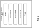
- FIG. 4 illustrates embodiments of execution unit(s) circuitry, such as execution unit(s) circuitry 362 of FIG. 3(B) .
- execution unit(s) circuity 362 may include one or more ALU circuits 401, vector/SIMD unit circuits 403, load/store unit circuits 405, and/or branch/jump unit circuits 407.
- ALU circuits 401 perform integer arithmetic and/or Boolean operations.
- Vector/SIMD unit circuits 403 perform vector/SIMD operations on packed data (such as SIMD/vector registers).
- Load/store unit circuits 405 execute load and store instructions to load data from memory into registers or store from registers to memory. Load/store unit circuits 405 may also generate addresses.
- Branch/jump unit circuits 407 cause a branch or jump to a memory address depending on the instruction.
- Floating-point unit (FPU) circuits 409 perform floating-point arithmetic.
- the width of the execution unit(s) circuitry 362 varies depending upon the embodiment and can range from 16-bit to 1,024-bit. In some embodiments, two or more smaller execution units are logically combined to form a larger execution unit (e.g., two 128-bit execution units are logically combined to form a 256-bit execution unit).
- FIG. 5 is a block diagram of a register architecture 500 according to some embodiments.
- the vector/SIMD registers 510 are physically 512-bits and, depending upon the mapping, only some of the lower bits are used.
- the vector/SIMD registers 510 are ZMM registers which are 512 bits: the lower 256 bits are used for YMM registers and the lower 128 bits are used for XMM registers. As such, there is an overlay of registers.
- a vector length field selects between a maximum length and one or more other shorter lengths, where each such shorter length is half the length of the preceding length.
- Scalar operations are operations performed on the lowest order data element position in a ZMM/YMM/XMM register; the higher order data element positions are either left the same as they were prior to the instruction or zeroed depending on the embodiment.
- the register architecture 500 includes writemask/predicate registers 515.
- writemask/predicate registers 515 there are 8 writemask/predicate registers (sometimes called k0 through k7) that are each 16-bit, 32-bit, 64-bit, or 128-bit in size.
- Writemask/predicate registers 515 may allow for merging (e.g., allowing any set of elements in the destination to be protected from updates during the execution of any operation) and/or zeroing (e.g., zeroing vector masks allow any set of elements in the destination to be zeroed during the execution of any operation).
- each data element position in a given writemask/predicate register 515 corresponds to a data element position of the destination.
- the writemask/predicate registers 515 are scalable and consists of a set number of enable bits for a given vector element (e.g., 8 enable bits per 64-bit vector element).
- the register architecture 500 includes a plurality of general-purpose registers 525. These registers may be 16-bit, 32-bit, 64-bit, etc. and can be used for scalar operations. In some embodiments, these registers are referenced by the names RAX, RBX, RCX, RDX, RBP, RSI, RDI, RSP, and R8 through R15.
- the register architecture 500 includes scalar floating-point register 545 which is used for scalar floating-point operations on 32/64/80-bit floating-point data using the x87 instruction set extension or as MMX registers to perform operations on 64-bit packed integer data, as well as to hold operands for some operations performed between the MMX and XMM registers.
- One or more flag registers 540 store status and control information for arithmetic, compare, and system operations.
- the one or more flag registers 540 may store condition code information such as carry, parity, auxiliary carry, zero, sign, and overflow.
- the one or more flag registers 540 are called program status and control registers.
- Segment registers 520 contain segment points for use in accessing memory. In some embodiments, these registers are referenced by the names CS, DS, SS, ES, FS, and GS.
- Machine specific registers (MSRs) 535 control and report on processor performance. Most MSRs 535 handle system-related functions and are not accessible to an application program. Machine check registers 560 consist of control, status, and error reporting MSRs that are used to detect and report on hardware errors.
- One or more instruction pointer register(s) 530 store an instruction pointer value.
- Control register(s) 555 e.g., CR0-CR4
- determine the operating mode of a processor e.g., processor 170, 180, 138, 115, and/or 200
- Debug registers 550 control and allow for the monitoring of a processor or core's debugging operations.
- Memory management registers 565 specify the locations of data structures used in protected mode memory management. These registers may include a GDTR, IDRT, task register, and a LDTR register.
- Alternative embodiments of the invention may use wider or narrower registers. Additionally, alternative embodiments of the invention may use more, less, or different register files and registers.
- An instruction set architecture may include one or more instruction formats.
- a given instruction format may define various fields (e.g., number of bits, location of bits) to specify, among other things, the operation to be performed (e.g., opcode) and the operand(s) on which that operation is to be performed and/or other data field(s) (e.g., mask).
- Some instruction formats are further broken down though the definition of instruction templates (or sub-formats).
- the instruction templates of a given instruction format may be defined to have different subsets of the instruction format's fields (the included fields are typically in the same order, but at least some have different bit positions because there are less fields included) and/or defined to have a given field interpreted differently.
- each instruction of an ISA is expressed using a given instruction format (and, if defined, in a given one of the instruction templates of that instruction format) and includes fields for specifying the operation and the operands.
- an exemplary ADD instruction has a specific opcode and an instruction format that includes an opcode field to specify that opcode and operand fields to select operands (source1/destination and source2); and an occurrence of this ADD instruction in an instruction stream will have specific contents in the operand fields that select specific operands.
- Embodiments of the instruction(s) described herein may be embodied in different formats. Additionally, exemplary systems, architectures, and pipelines are detailed below. Embodiments of the instruction(s) may be executed on such systems, architectures, and pipelines, but are not limited to those detailed.
- FIG. 6 illustrates embodiments of an instruction format.
- an instruction may include multiple components including, but not limited to, one or more fields for: one or more prefixes 601, an opcode 603, addressing information 605 (e.g., register identifiers, memory addressing information, etc.), a displacement value 607, and/or an immediate 609.
- addressing information 605 e.g., register identifiers, memory addressing information, etc.
- a displacement value 607 e.g., a displacement value, and/or an immediate 609.
- some instructions utilize some or all of the fields of the format whereas others may only use the field for the opcode 603.
- the order illustrated is the order in which these fields are to be encoded, however, it should be appreciated that in other embodiments these fields may be encoded in a different order, combined, etc.
- the prefix(es) field(s) 601 when used, modifies an instruction.
- one or more prefixes are used to repeat string instructions (e.g., 0xF0, 0xF2, 0xF3, etc.), to provide section overrides (e.g., 0x2E, 0x36, 0x3E, 0x26, 0x64, 0x65, 0x2E, 0x3E, etc.), to perform bus lock operations, and/or to change operand (e.g., 0x66) and address sizes (e.g., 0x67).
- Certain instructions require a mandatory prefix (e.g., 0x66, 0xF2, 0xF3, etc.). Certain of these prefixes may be considered “legacy" prefixes. Other prefixes, one or more examples of which are detailed herein, indicate, and/or provide further capability, such as specifying particular registers, etc. The other prefixes typically follow the "legacy" prefixes.
- the opcode field 603 is used to at least partially define the operation to be performed upon a decoding of the instruction.
- a primary opcode encoded in the opcode field 603 is 1, 2, or 3 bytes in length. In other embodiments, a primary opcode can be a different length. An additional 3-bit opcode field is sometimes encoded in another field.
- the addressing field 605 is used to address one or more operands of the instruction, such as a location in memory or one or more registers.
- FIG. 7 illustrates embodiments of the addressing field 605.
- an optional ModR/M byte 702 and an optional Scale, Index, Base (SIB) byte 704 are shown.
- the ModR/M byte 702 and the SIB byte 704 are used to encode up to two operands of an instruction, each of which is a direct register or effective memory address. Note that each of these fields are optional in that not all instructions include one or more of these fields.
- the MOD R/M byte 702 includes a MOD field 742, a register field 744, and R/M field 746.
- the content of the MOD field 742 distinguishes between memory access and non-memory access modes.
- a register-direct addressing mode is utilized, and otherwise register-indirect addressing is used.
- the register field 744 may encode either the destination register operand or a source register operand, or may encode an opcode extension and not be used to encode any instruction operand.
- the content of register index field 744 directly or through address generation, specifies the locations of a source or destination operand (either in a register or in memory).
- the register field 744 is supplemented with an additional bit from a prefix (e.g., prefix 601) to allow for greater addressing.
- the R/M field 746 may be used to encode an instruction operand that references a memory address, or may be used to encode either the destination register operand or a source register operand. Note the R/M field 746 may be combined with the MOD field 742 to dictate an addressing mode in some embodiments.
- the SIB byte 704 includes a scale field 752, an index field 754, and a base field 756 to be used in the generation of an address.
- the scale field 752 indicates scaling factor.
- the index field 754 specifies an index register to use. In some embodiments, the index field 754 is supplemented with an additional bit from a prefix (e.g., prefix 601) to allow for greater addressing.
- the base field 756 specifies a base register to use. In some embodiments, the base field 756 is supplemented with an additional bit from a prefix (e.g., prefix 601) to allow for greater addressing.
- the content of the scale field 752 allows for the scaling of the content of the index field 754 for memory address generation (e.g., for address generation that uses 2 scale ⁇ index + base).
- a memory address may be generated according to 2 scale ⁇ index + base + displacement, index ⁇ scale+displacement, r/m + displacement, instruction pointer (RIP/EIP) + displacement, register + displacement, etc.
- the displacement may be a 1-byte, 2-byte, 4-byte, etc. value.
- a displacement field 607 provides this value.
- a displacement factor usage is encoded in the MOD field of the addressing field 605 that indicates a compressed displacement scheme for which a displacement value is calculated by multiplying disp8 in conjunction with a scaling factor N that is determined based on the vector length, the value of a b bit, and the input element size of the instruction.
- the displacement value is stored in the displacement field 607.
- an immediate field 609 specifies an immediate for the instruction.
- An immediate may be encoded as a 1-byte value, a 2-byte value, a 4-byte value, etc.
- FIG. 8 illustrates embodiments of a first prefix 601(A).
- the first prefix 601(A) is an embodiment of a REX prefix. Instructions that use this prefix may specify general purpose registers, 64-bit packed data registers (e.g., single instruction, multiple data (SIMD) registers or vector registers), and/or control registers and debug registers (e.g., CR8-CR15 and DR8-DR15).
- SIMD single instruction, multiple data
- Instructions using the first prefix 601(A) may specify up to three registers using 3-bit fields depending on the format: 1) using the reg field 744 and the R/M field 746 of the Mod R/M byte 702; 2) using the Mod R/M byte 702 with the SIB byte 704 including using the reg field 744 and the base field 756 and index field 754; or 3) using the register field of an opcode.
- bit positions 7:4 are set as 0100.
- bit position 2 may an extension of the MOD R/M reg field 744 and may be used to modify the ModR/M reg field 744 when that field encodes a general purpose register, a 64-bit packed data register (e.g., a SSE register), or a control or debug register. R is ignored when Mod R/M byte 702 specifies other registers or defines an extended opcode.
- Bit position 1 (X) X bit may modify the SIB byte index field 754.
- Bit position B (B) B may modify the base in the Mod R/M R/M field 746 or the SIB byte base field 756; or it may modify the opcode register field used for accessing general purpose registers (e.g., general purpose registers 525).
- FIGS. 9(A) -(D) illustrate embodiments of how the R, X, and B fields of the first prefix 601(A) are used.
- FIG. 9(A) illustrates R and B from the first prefix 601(A) being used to extend the reg field 744 and R/M field 746 of the MOD R/M byte 702 when the SIB byte 7 04 is not used for memory addressing.
- FIG. 9(B) illustrates R and B from the first prefix 601(A) being used to extend the reg field 744 and R/M field 746 of the MOD R/M byte 702 when the SIB byte 7 04 is not used (register-register addressing).
- FIG. 9(A) illustrates R and B from the first prefix 601(A) being used to extend the reg field 744 and R/M field 746 of the MOD R/M byte 702 when the SIB byte 7 04 is not used (register-register addressing).
- FIG. 9(A) illustrates R and B from the first
- FIG. 9(C) illustrates R, X, and B from the first prefix 601(A) being used to extend the reg field 744 of the MOD R/M byte 702 and the index field 754 and base field 756 when the SIB byte 7 04 being used for memory addressing.
- FIG. 9(D) illustrates B from the first prefix 601(A) being used to extend the reg field 744 of the MOD R/M byte 702 when a register is encoded in the opcode 603.
- FIGS. 10(A) -(B) illustrate embodiments of a second prefix 601(B).
- the second prefix 601(B) is an embodiment of a VEX prefix.
- the second prefix 601(B) encoding allows instructions to have more than two operands, and allows SIMD vector registers (e.g., vector/SIMD registers 510) to be longer than 64-bits (e.g., 128-bit and 256-bit).
- SIMD vector registers e.g., vector/SIMD registers 510) to be longer than 64-bits (e.g., 128-bit and 256-bit).
- the second prefix 601(B) comes in two forms - a two-byte form and a three-byte form.
- the two-byte second prefix 601(B) is used mainly for 128-bit, scalar, and some 256-bit instructions; while the three-byte second prefix 601(B) provides a compact replacement of the first prefix 601(A) and 3-byte opcode instructions.
- FIG. 10(A) illustrates embodiments of a two-byte form of the second prefix 601(B).
- a format field 1001 (byte 0 1003) contains the value C5H.
- byte 1 1005 includes a "R" value in bit[7]. This value is the complement of the same value of the first prefix 601(A).
- Bit[2] is used to dictate the length (L) of the vector (where a value of 0 is a scalar or 128-bit vector and a value of 1 is a 256-bit vector).
- Bits[6:3] shown as vvvv may be used to: 1) encode the first source register operand, specified in inverted (1s complement) form and valid for instructions with 2 or more source operands; 2) encode the destination register operand, specified in Is complement form for certain vector shifts; or 3) not encode any operand, the field is reserved and should contain a certain value, such as 1111b.
- Instructions that use this prefix may use the Mod R/M R/M field 746 to encode the instruction operand that references a memory address or encode either the destination register operand or a source register operand.
- Instructions that use this prefix may use the Mod R/M reg field 744 to encode either the destination register operand or a source register operand, be treated as an opcode extension and not used to encode any instruction operand.
- vvvv For instruction syntax that support four operands, vvvv, the Mod R/M R/M field 746 and the Mod R/M reg field 744 encode three of the four operands. Bits[7:4] of the immediate 609 are then used to encode the third source register operand.
- FIG. 10(B) illustrates embodiments of a three-byte form of the second prefix 601(B).
- a format field 1011 (byte 0 1013) contains the value C4H.
- Byte 1 1015 includes in bits[7:5] "R,” "X,” and "B” which are the complements of the same values of the first prefix 601(A).
- Bits[4:0] of byte 1 1015 (shown as mmmmm) include content to encode, as need, one or more implied leading opcode bytes. For example, 00001 implies a 0FH leading opcode, 00010 implies a 0F38H leading opcode, 00011 implies a leading 0F3AH opcode, etc.
- Bit[7] of byte 2 1017 is used similar to W of the first prefix 601(A) including helping to determine promotable operand sizes.
- Bit[2] is used to dictate the length (L) of the vector (where a value of 0 is a scalar or 128-bit vector and a value of 1 is a 256-bit vector).
- Bits[6:3], shown as vvvv may be used to: 1) encode the first source register operand, specified in inverted (1s complement) form and valid for instructions with 2 or more source operands; 2) encode the destination register operand, specified in Is complement form for certain vector shifts; or 3) not encode any operand, the field is reserved and should contain a certain value, such as 1111b.
- Instructions that use this prefix may use the Mod R/M R/M field 746 to encode the instruction operand that references a memory address or encode either the destination register operand or a source register operand.
- Instructions that use this prefix may use the Mod R/M reg field 744 to encode either the destination register operand or a source register operand, be treated as an opcode extension and not used to encode any instruction operand.
- vvvv For instruction syntax that support four operands, vvvv, the Mod R/M R/M field 746, and the Mod R/M reg field 744 encode three of the four operands. Bits[7:4] of the immediate 609 are then used to encode the third source register operand.
- FIG. 11 illustrates embodiments of a third prefix 601(C).
- the first prefix 601(A) is an embodiment of an EVEX prefix.
- the third prefix 601(C) is a four-byte prefix.
- the third prefix 601(C) can encode 32 vector registers (e.g., 128-bit, 256-bit, and 512-bit registers) in 64-bit mode.
- instructions that utilize a writemask/opmask see discussion of registers in a previous figure, such as FIG. 5 ) or predication utilize this prefix.
- Opmask register allow for conditional processing or selection control.
- Opmask instructions, whose source/destination operands are opmask registers and treat the content of an opmask register as a single value, are encoded using the second prefix 601(B).
- the third prefix 601(C) may encode functionality that is specific to instruction classes (e.g., a packed instruction with "load+op" semantic can support embedded broadcast functionality, a floating-point instruction with rounding semantic can support static rounding functionality, a floating-point instruction with non-rounding arithmetic semantic can support "suppress all exceptions" functionality, etc.).
- instruction classes e.g., a packed instruction with "load+op" semantic can support embedded broadcast functionality, a floating-point instruction with rounding semantic can support static rounding functionality, a floating-point instruction with non-rounding arithmetic semantic can support "suppress all exceptions" functionality, etc.
- the first byte of the third prefix 601(C) is a format field 1111 that has a value, in one example, of 62H. Subsequent bytes are referred to as payload bytes 1115-1119 and collectively form a 24-bit value of P[23:0] providing specific capability in the form of one or more fields (detailed herein).
- P[1:0] of payload byte 1119 are identical to the low two mmmmm bits.
- P[3:2] are reserved in some embodiments.
- Bit P[4] (R') allows access to the high 16 vector register set when combined with P[7] and the ModR/M reg field 744.
- P[6] can also provide access to a high 16 vector register when SIB-type addressing is not needed.
- P[7:5] consist of an R, X, and B which are operand specifier modifier bits for vector register, general purpose register, memory addressing and allow access to the next set of 8 registers beyond the low 8 registers when combined with the ModR/M register field 744 and ModR/M R/M field 746.
- P[10] in some embodiments is a fixed value of 1.
- P[14:11], shown as vvvv, may be used to: 1) encode the first source register operand, specified in inverted (1s complement) form and valid for instructions with 2 or more source operands; 2) encode the destination register operand, specified in Is complement form for certain vector shifts; or 3) not encode any operand, the field is reserved and should contain a certain value, such as 1111b.
- P[15] is similar to W of the first prefix 601(A) and second prefix 611(B) and may serve as an opcode extension bit or operand size promotion.
- P[18:16] specify the index of a register in the opmask (writemask) registers (e.g., writemask/predicate registers 515).
- vector masks allow any set of elements in the destination to be protected from updates during the execution of any operation (specified by the base operation and the augmentation operation); in other one embodiment, preserving the old value of each element of the destination where the corresponding mask bit has a 0.
- any set of elements in the destination when zeroing vector masks allow any set of elements in the destination to be zeroed during the execution of any operation (specified by the base operation and the augmentation operation); in one embodiment, an element of the destination is set to 0 when the corresponding mask bit has a 0 value.
- a subset of this functionality is the ability to control the vector length of the operation being performed (that is, the span of elements being modified, from the first to the last one); however, it is not necessary that the elements that are modified be consecutive.
- the opmask field allows for partial vector operations, including loads, stores, arithmetic, logical, etc.
- opmask field's content selects one of a number of opmask registers that contains the opmask to be used (and thus the opmask field's content indirectly identifies that masking to be performed)
- alternative embodiments instead or additional allow the mask write field's content to directly specify the masking to be performed.
- P[19] can be combined with P[14:11] to encode a second source vector register in a non-destructive source syntax which can access an upper 16 vector registers using P[19].
- P[20] encodes multiple functionalities, which differs across different classes of instructions and can affect the meaning of the vector length/ rounding control specifier field (P[22:21]).
- P[23] indicates support for merging-writemasking (e.g., when set to 0) or support for zeroing and merging-writemasking (e.g., when set to 1).
- Table 1 32-Register Support in 64-bit Mode 4 3 [2:0] REG. TYPE COMMON USAGES REG R' R ModR/M reg GPR, Vector Destination or Source VVVV V' vvv GPR, Vector 2nd Source or Destination RM X B ModR/M R/M GPR, Vector 1st Source or Destination BASE 0 B ModR/M R/M GPR Memory addressing INDEX 0 X SIB.index GPR Memory addressing VIDX V' X SIB.index Vector VSIB memory addressing Table 2: Encoding Register Specifiers in 32-bit Mode [2:0] REG.
- Program code may be applied to input instructions to perform the functions described herein and generate output information.
- the output information may be applied to one or more output devices, in known fashion.
- a processing system includes any system that has a processor, such as, for example, a digital signal processor (DSP), a microcontroller, an application specific integrated circuit (ASIC), or a microprocessor.
- DSP digital signal processor
- ASIC application specific integrated circuit
- the program code may be implemented in a high-level procedural or object-oriented programming language to communicate with a processing system.
- the program code may also be implemented in assembly or machine language, if desired.
- the mechanisms described herein are not limited in scope to any particular programming language. In any case, the language may be a compiled or interpreted language.
- Embodiments of the mechanisms disclosed herein may be implemented in hardware, software, firmware, or a combination of such implementation approaches.
- Embodiments of the invention may be implemented as computer programs or program code executing on programmable systems comprising at least one processor, a storage system (including volatile and non-volatile memory and/or storage elements), at least one input device, and at least one output device.
- IP cores may be stored on a tangible, machine readable medium and supplied to various customers or manufacturing facilities to load into the fabrication machines that actually make the logic or processor.
- Such machine-readable storage media may include, without limitation, non-transitory, tangible arrangements of articles manufactured or formed by a machine or device, including storage media such as hard disks, any other type of disk including floppy disks, optical disks, compact disk read-only memories (CD-ROMs), compact disk rewritable's (CD-RWs), and magneto-optical disks, semiconductor devices such as read-only memories (ROMs), random access memories (RAMs) such as dynamic random access memories (DRAMs), static random access memories (SRAMs), erasable programmable read-only memories (EPROMs), flash memories, electrically erasable programmable read-only memories (EEPROMs), phase change memory (PCM), magnetic or optical cards, or any other type of media suitable for storing electronic instructions.
- storage media such as hard disks, any other type of disk including floppy disks, optical disks, compact disk read-only memories (CD-ROMs), compact disk rewritable's (CD-RWs), and magneto
- embodiments of the invention also include non-transitory, tangible machine-readable media containing instructions or containing design data, such as Hardware Description Language (HDL), which defines structures, circuits, apparatuses, processors and/or system features described herein.
- HDL Hardware Description Language
- Such embodiments may also be referred to as program products.
- Emulation including binary translation, code morphing, etc.
- an instruction converter may be used to convert an instruction from a source instruction set to a target instruction set.
- the instruction converter may translate (e.g., using static binary translation, dynamic binary translation including dynamic compilation), morph, emulate, or otherwise convert an instruction to one or more other instructions to be processed by the core.
- the instruction converter may be implemented in software, hardware, firmware, or a combination thereof.
- the instruction converter may be on processor, off processor, or part on and part off processor.
- FIG. 12 illustrates a block diagram contrasting the use of a software instruction converter to convert binary instructions in a source instruction set to binary instructions in a target instruction set according to certain implementations.
- the instruction converter is a software instruction converter, although alternatively the instruction converter may be implemented in software, firmware, hardware, or various combinations thereof.
- FIG. 12 shows a program in a high level language 1202 may be compiled using a first ISA compiler 1204 to generate first ISA binary code 1206 that may be natively executed by a processor with at least one first instruction set core 1216.
- the processor with at least one first ISA instruction set core 1216 represents any processor that can perform substantially the same functions as an Intel ® processor with at least one first ISA instruction set core by compatibly executing or otherwise processing (1) a substantial portion of the instruction set of the first ISA instruction set core or (2) object code versions of applications or other software targeted to run on an Intel processor with at least one first ISA instruction set core, in order to achieve substantially the same result as a processor with at least one first ISA instruction set core.
- the first ISA compiler 1204 represents a compiler that is operable to generate first ISA binary code 1206 (e.g., object code) that can, with or without additional linkage processing, be executed on the processor with at least one first ISA instruction set core 1216.
- FIG. 12 shows the program in the high level language 1202 may be compiled using an alternative instruction set compiler 1208 to generate alternative instruction set binary code 1210 that may be natively executed by a processor without a first ISA instruction set core 1214.
- the instruction converter 1212 is used to convert the first ISA binary code 1206 into code that may be natively executed by the processor without a first ISA instruction set core 1214.
- This converted code is not likely to be the same as the alternative instruction set binary code 1210 because an instruction converter capable of this is difficult to make; however, the converted code will accomplish the general operation and be made up of instructions from the alternative instruction set.
- the instruction converter 1212 represents software, firmware, hardware, or a combination thereof that, through emulation, simulation or any other process, allows a processor or other electronic device that does not have a first ISA instruction set processor or core to execute the first ISA binary code 1206.
- a device may service or otherwise support multiple clients.
- the scalability of a device may be limited by its capability to maintain information about each of the different clients that it is servicing, which in turn may be limited by the silicon die area or other space available to store such information.
- SR-IOV single-root input/output virtualization
- PCIe Peripheral Component Interconnect Express
- VFs virtual functions
- a device can also implement a larger number of queues and associated client-specific state to support a larger number of clients.
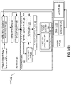
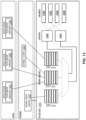
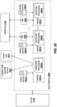
- FIG. 13 illustrates one embodiment of a scalable device 100 which may be implemented in logic gates, storage elements, and/or any other type of circuitry, all or parts of which may be included in a discrete component and/or integrated into the circuitry of a processing device or any other apparatus in a computer or other information processing system.
- device 1300 in FIG. 13 may correspond to coprocessor 138 in FIG. 1 or special purpose logic 208 in FIG. 2 .
- a scalable device may use any number of work queues 1350, where a work queue is a data structure to be used to accept work from clients.
- a work queue may be a dedicated work queue (DWQ) that may accept work from a single client or a shared work queue (SWQ) that may accept work from multiple clients.
- DWQ dedicated work queue
- SWQ shared work queue
- device 1300 is shown as including DWQs 1310 and 1314 and SWQ 1312, which may accept work from clients 1320, 1322, 1324, 1326, and 1328.
- a work queue may be implemented using memory within the device (e.g., device 1300) and/or using memory not within the device (e.g., host memory, system memory, registers or other storage locations not within the device).
- a work queue 1350 may be implemented with a base register, a head register, and a tail register that are writable by software to inform the device about work submission.
- a work queue 1350 may be implemented with an address to which software may write to submit work.
- Work queues 1350 may be used to store work descriptors that include a client identifier (ID) and privileges.
- ID is to identify the client (e.g., with a process address space identifier (PASID)) and the privileges indicate the privileges that the device may use to identify the address domain and privileges of the client.
- Work descriptors may be populated by trusted hardware (e.g., a CPU in a secured environment) and/or trusted software (an operating system (OS) running on a CPU in a secured environment) to ensure that they cannot be spoofed by unprivileged clients.
- trusted hardware e.g., a CPU in a secured environment
- OS operating system
- work descriptors are fully self-describing so that the device does not need to retain any client-specific state, and thus does not require additional memory to support additional clients.
- a fully self-describing work descriptor contains all the information needed to perform the work requested.
- a work descriptor in an embodiment may include a pointer to a completion record in host memory where completion status (including any error status) is to be written.
- a completion record may also contain any partial results that a subsequent work descriptor may use, so that data may be carried forward through operations (e.g., a cyclic redundancy check computation may use the result from each step as an input to the next step).
- a completion record may also contain flag bits and/or any other information that may be used in performing operations. Therefore, no memory within the device will be used to store per-client state regarding completion status, partial results, flag bits, etc.
- work descriptors may also be used to avoid other limits on the scalability of the device. For example, limiting the number of clients to one per messaged-signaled interrupt in a PCI MSI-X table in the device may be avoided according to either of the following approaches. According to either approach, any client may be set up with multiple interrupts so that the client can choose to specify different interrupts for different descriptors, thus allowing the client to perform interrupt rebalancing without involving OS or other system software.
- a work descriptor may be designed to include interrupt message information (e.g., MSI address and data) passed in by the client. Since the interrupt message is provided by the client, it is untrusted, so interrupt remapping hardware (e.g., an I/O memory management unit) may be responsible for ensuring that a client cannot request an interrupt that is not assigned to it. For example, a PASID along with a remappable interrupt message may be used to locate an Interrupt Remapping Table Entry for the interrupt message (PASID granular interrupt remapping).
- interrupt message information e.g., MSI address and data
- interrupt remapping hardware e.g., an I/O memory management unit
- a PASID along with a remappable interrupt message may be used to locate an Interrupt Remapping Table Entry for the interrupt message (PASID granular interrupt remapping).
- PASID granular interrupt remapping allows the same message to have different meanings when used in conjunction with different PASIDs, and it also allows system software to control which interrupt messages may be used by each client (as identified by the client's PASID). Then, the device can use the interrupt message information from the work descriptor to generate the interrupt when it is done with the operation, while avoiding storing interrupt messages in the device.
- a work descriptor may be designed to include an interrupt handle (instead of the full MSI address and data values).
- the interrupt handle in the descriptor designates an entry in an interrupt message table.
- the device may implement the interrupt message table in host memory, with each interrupt table entry containing the MSI address and data. Since the interrupt message table is in host memory rather than device memory, it can be made large enough to support any number of clients.
- the interrupt handle in the work descriptor may be used by the device to index into the interrupt table to identify the MSI address and data values for generating the interrupt when the device is done with the operation. The device will first validate the interrupt handle using the PASID to ensure the client is allowed to use the specific interrupt handle.
- the device may validate the interrupt handle by using PASID granular interrupt message tables or by including the PASID in the interrupt table entry during interrupt setup and generation, matching the entry's PASID against client's PASID.
- an interrupt message cache within the device may cache frequently used interrupt entries.
- Embodiments provide for efficiently processing work from many clients.
- Embodiments may allow prioritization of work from time-sensitive clients while ensuring forward-progress on work from other clients.
- Embodiments may prevent errors or performance issues due to some clients from negatively affecting other clients.
- a work submission portal is a means by which clients may submit work requests to a device.
- an SWQ may have more than one work submission portal to which clients may submit work, rather than a single work submission portal mapped to all clients using the SWQ.
- the use of a single work submission portal per SWQ may cause clients to keep retrying work submissions because they experience the SWQ as full, which may make the use of the device difficult and unpredictable for other clients.
- the use of multiple work submission queues per SWQ may provide for prioritization of work requests and prevention of starvation of some clients.
- work submission portals may be implemented as memory mapped I/O (MMIO) addresses to which clients may write to submit work requests, so multiple work submission portals may be provided by assigning more than one MMIO address to an SWQ and providing different MMIO addresses to different clients, which does not require additional logic circuitry or storage in the device.
- MMIO memory mapped I/O
- different work submission portals for an SWQ may have different characteristics, such as different work acceptance priorities for different clients.
- an SWQ may have a first submission portal designated as a limited portal and a second submission portal designated as an unlimited portal.
- the SWQ may have a configurable threshold that may be used to reserve some entries exclusively for work submitted through the unlimited portal.
- the SWQ may be configured to use only up to 80% (threshold) of the SWQ space for work submitted through the limited portal, while work submitted through the unlimited portal may use 100% of the SWQ space.
- privileged software e.g., the device driver
- user space clients experience an SWQ full condition (e.g., the SWQ returns 'Retry' to user space clients when the SWQ is 80% full)
- they can make a request to the device driver to submit the work descriptor on their behalf.
- the device driver can serialize requests from user space clients and use the unlimited portal to submit work requests. Since 20% of the SWQ space is reserved for the unlimited portal, the device driver's work submission will likely succeed.
- Embodiments may also provide for handling situations in which the SWQ is 100% full (e.g., even the unlimited portal returns 'Retry').
- the device driver may respond to the client with 'Retry' as if 'Retry' had been received directly from the device.
- the device driver may block the client until the work can be submitted, and the device driver may possibly schedule another client in the meantime.
- the device driver may place the work descriptor in a software-defined work queue until it can be submitted to the device, but resume the client as if the work had been successfully submitted to the device. According to this latter approach, the client may continue operation while waiting for the device to catch up.
- Embodiments may provide for the use of this latter approach, by ensuring that all descriptors to the device are independent of each other with respect to ordering or by preventing the client from submitting any descriptors directly to the device that could be processed prior to the descriptor that was queued in software by the device driver. This prevention may be achieved by removing the device submission portal from the client's memory map so the client cannot submit work to the device directly or by locking the SWQ so that no clients can submit work.
- Embodiments may also provide for configurability of the work queues themselves. For example, any or each of the multiple work queues may be configured, at run-time based on client requirements, as dedicated or shared. Work queues may be assigned different priorities and configured by software. The device may dispatch commands from higher priority work queues preferentially over commands from lower priority work queues without starving the lower priority work queues. Some clients may have access to multiple work queues, and thus have the ability to prioritize their own work, while other clients may have access to only a single work queue, thus fixing the priority of all work they submit.
- Embodiments may also provide for alleviating a problem which occurs when a device is blocked because it is waiting for a response from another part of the system (e.g., completion of a memory read, translation of address, handling of page fault) while performing an operation.
- This problem is called head-of-line blocking, because the operation being performed in the device prevents other operations in line behind it from making progress.
- a device may include multiple operation components (engines) that can process individual work descriptors in parallel, such as engines 1330, 1332, 1334, and 1336.
- one or more work queues may be grouped together with one or more engines.
- a device may support several groups, such as groups 1340 and 1342. Each work queue and each engine may be configured by software to be part of any one group. Work descriptors from one or more work queues in a group may be dispatched to any of the engines in that group. Thus, if one engine in a group is waiting for an external response while processing a descriptor from a work queue, other engines in the group may continue to process other work descriptors from the same or other work queues.
- a device may implement an out-of-order processing engine, which may suspend a work descriptor that is waiting for an external response, and process other work descriptors in the meantime from the same or other work queues.
- a device may have internal resources (e.g., device internal memory) that engines use to process work descriptors from various clients. If these resources are limited, the device may prioritize (or provide QoS for) use of these resources by different clients to ensure that work descriptors (e.g., relatively large or time-consuming ones) from one or a few clients do not consume most or all internal resources, thereby affecting the processing of other clients and overall performance of the device.
- the prioritization may be done using a credit-based system in which credits represent the internal resources. Credits may be assigned to groups, individual work queues, or individual engines to control the number of resources each group, work queue, or engine is allowed to use to process its work descriptors.
- a device may define two credit thresholds for each group, work queue, or engine: a first threshold to specify a minimum number of credits reserved for a group, work queue, or engine (minimum guaranteed or reserved credits), and a second threshold to specify a maximum number of credits allowed for a group, work queue, or engine (maximum allowed credits).
- Embodiments may also provide for efficient handling of page faults. If a device supports virtual memory (e.g., shared virtual memory (SVM) or I/O virtual addresses (IOVA)), the addresses given to the device in work descriptors are not guaranteed to be mapped in physical memory. Before accessing host memory (e.g., through direct memory access (DMA)), the device may request address translation from an I/O memory management unit (IOMMU), using, for example, the Address Translation Services described in the PCIe specification. The IOMMU walks the address translation tables and, if a translation is present, returns the translated physical address to the device so that the device can access the data in memory.
- virtual memory e.g., shared virtual memory (SVM) or I/O virtual addresses (IOVA)
- DMA direct memory access
- IOMMU I/O memory management unit
- the IOMMU walks the address translation tables and, if a translation is present, returns the translated physical address to the device so that the device can access the data in memory.
- a page fault may also occur when a page is present, but the processor or device does not have rights to perform the type of access requested (e.g., a device attempts to write to a read-only page).
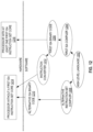
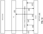
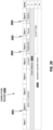
- a device When a device encounters a page fault, it cannot handle the page fault itself because the memory management system software does not run on the device. Therefore, according to a method (1400) illustrated in FIG. 14 , after the application submits a command to the device (1410), the device attempts to access the page (1420), and the IOMMU responds with a page fault (1430), the device sends a page fault notification through the IOMMU to the OS (1440) and blocks the descriptor processing until the page fault is resolved. After resolving the page fault (1450), the OS responds back to the device, through the IOMMU, that the page is available (1460). Then, the device attempts to re-access the page, and this time the access is successful (1470).
- a device typically implements a limited number of simultaneous outstanding I/O page fault notifications to the OS. Hence, when supporting a large number of clients, the device may encounter many page faults and may usually be waiting for at least one page fault to be resolved, which will significantly reduce the performance of the device.
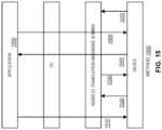
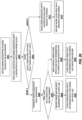
- some implementations may include (after the application submits a command to the device (1510), the device attempts to access the page (1520), and the IOMMU responds with a page fault (1530)), the device directly notifying the client about a page fault (1540) and terminate processing of the work descriptor that caused the page fault. Then, the device may continue processing other work descriptors without blocking while the application may resolve or otherwise respond to (as described below) the page fault (1550). After the page fault is resolved, the application may resubmit the command to the device (1560) and the device may attempt to re-access the page (1570).
- page fault handing may be left to the client.
- the client application may request the OS to resolve the page fault (e.g., by accessing the faulting pages) and resubmit a work descriptor to resume the work after the page fault is resolved.
- the client may decide to complete the remaining work using some other method instead of using the device, such as by using the CPU to perform the operation.
- the mechanism used by the device to notify the application that it has encountered a page fault is called partial completion.
- the device may report completion of the operation to the client in the normal way (e.g., by setting a device register, modifying the tail pointer of a queue or ring buffer, writing to a shared memory location, generating an interrupt, or any combination of these), but the completion record information may include the following additional elements: a status field indicating that a page fault was encountered, an indication of how much of the operation completed prior to the page fault, the virtual address that could not be translated, an indication of whether the device intended to read or write to the address that could not be translated, and any other information needed by software to resume the operation (see examples below).
- partial completion means that the device may have performed part of the requested operation prior to encountering the page fault.
- the client e.g., application software
- the client may begin using the results that have been completed, even while the page fault is being resolved and the remainder of the operation is being performed by the device.
- a partial completion may report that none of the operation has been completed, if, for example, the device encounters a page fault on the first page that is needed to begin the operation.
- the device may restart the operation from the beginning rather than resume from the point where it encountered the page fault. In this case, the device may report that none of the operation has completed, even when the page fault was not on the first page (assuming that the partially completed operation has not overwritten any of its inputs).
- the partial completion information includes all information required to resume the operation.
- the client may resume the operation by submitting a new command that starts where the previous operation stopped.
- For operations that carry forward data throughout the operation e.g., CRC computation
- the intermediate result is retained for use when the operation is resumed.
- the intermediate result may be saved in the completion record along with the page fault information.
- Accelerators are frequently configured to use shared virtual memory (SVM), which provides a ubiquitous programming model between the host/CPU and accelerator offloads.
- SVM shared virtual memory
- VM or containers highly multi-tenanted environments
- Accelerator modes such as SVM Block-on-Fault and SVM Fault-and-Stream have been used to address these limitations.
- SVM Block-on-Fault the accelerator/engine blocks until the I/O page-fault is resolved by the OS/VMM software and a response is returned to continue the remaining work.
- SVM Fault-and-Stream the Accelerator/Engine context switches to another offload-context while the I/O page-fault is resolved for given context.
- SVM Block-on-Fault has scaling and multi-tenant challenges. If the accelerator has only 4 engines, the I/O page-fault cannot scale beyond four concurrent clients or has noisy neighbor-related challenges with multi-tenancy (e.g. a page-fault from one tenant will delay offload execution for other tenants). SVM Fault-and-Stream has challenges with respect the added device complexity and overheads associated with saving/restoring state. Moreover, previous techniques only support page-faults on data-buffers and not on the control structures.
- the embodiments of the invention include techniques to support high-performance I/O page-fault handling for accelerator devices in highly multi-tenant and scalable environments, while keeping accelerator complexity and cost in check.
- the implementations described herein provide page-fault handling for accelerators which have per-work queue capability, directly notifying application/offload-clients about accelerator page-faults, and providing event-log mechanisms to allow the accelerator driver to proxy the page-fault handling/notification to offload clients (when direct notification is not feasible/recommended).
- some embodiments can prematurely complete the execution of a faulted context and immediately switch to the next context, allowing software to handle the page-fault and complete the remaining work either on the host processor (e.g., CPU) or by offloading again to the accelerator.
- extensions are described for handling batch descriptors.
- an accelerator 1600 includes a work acceptance unit 1610 comprising a plurality of work queues (WQs) 1601A-D which may be arranged into groups based on workload characteristics as described above.
- a plurality of execution units, or "engines" 1621A-D are assigned to process work descriptors from one or more of the work queues 1601A-D.
- One or more work dispatchers 1630 dispatches the work specified in the descriptors from the work queues 1601A-D to the execution engines 1621A-D.
- Execution engines 1621A-D are typically shared between multiple clients, which may be drivers, applications, virtual machines (VMs), containers, or any other functional software component. Resource sharing reduces the cost/burden of building independent engines for each client.
- the work queues 1601A-D funnel work to these engines 1621A-D and are either assigned to individual clients (e.g., the dedicated work queues 1310, 1314 in Figure 13 ) or shared between them (e.g., the shared work queue 1312 in Figure 13 ).
- the accelerator 1600 will attempt to acquire address translations associated with the addresses specified in the work-descriptors, for example, by using PCIe Address Translation Services.
- An accelerator 1600 may include a translation lookaside buffer 1705 to cache virtual-to-physical address translations. If a particular translation is not found in the TLB 1705, a translation request 1750 is sent to the IOMMU 1725 within a root complex 1720 of the host processor 1710. The IOMMU will retrieve the translation from its TLB or retrieve it from memory 1715 and will then transmit a translation response 1751 to the accelerator 1600 with the translation.
- the IOMMU 1725 and accelerator 1600 must communicate to ensure that the TLB 1705 of the accelerator 1600 remains consistent with the TLB of the IOMMU 1725 and host processors 1710. Thus, in response to certain events such as the modification of translation entries or context switches, the IOMMU 1725 will transmit invalidation requests 1753 to the accelerator 1600 which will invalidate the relevant TLB entries and send back an invalidation acknowledgement response 1754 when complete.
- the translation request 1750 will generate a page-request 1755, for example, by using PCIe Page Request Services.
- a page-request is received by the IOMMU 1725 and passed on to system software (e.g., OS/VMM) to process an I/O page-fault.
- system software e.g., OS/VMM
- System software will fix the page-fault and return a successful page-response 1756 to the accelerator device via the IOMMU 1725.
- a page-response with a corresponding error is returned to the accelerator 1600.
- the accelerator 1600 (or engine of the accelerator) can stall the engine/execution until the I/O page-fault is processed (similar to how an application running on a core is stalled until a CPU page-fault is handled), referred to as "SVM Block-on-Fault Mode".
- the accelerator/engine can generate the page-request, save the current work-context and transition to the next work-descriptor, resuming work later once the page-fault is handled, referred to as "SVM Fault-and-Stream Mode".
- Block-on-Fault mode has scaling and noisy neighbor related challenges. For example, in a scenario where 4 work queues associated with 4 different clients are mapped to an engine, a page-fault from one client will cause the engine to stall resulting in delayed execution for the other clients. This becomes even more of a problem with virtualized configurations, where page-fault handling latencies are higher and behavior of one VM/tenant will impact quality of service for other VMs/tenants sharing the same engine.
- Fault-and-Stream mode attempts to address this stalling problem; however, it requires complex hardware that can support saving and restoring of workload context and has challenges with respect to cost/latencies associated with context switching and the save/restore operations.
- Figure 18 illustrates an example of an accelerator 1800 on which embodiments of the invention may be implemented.
- a plurality of engines 1821A-C process descriptors from a plurality of work queues 1801A-C.
- the accelerator engines 1821A-C each include fault processing logic 1805A-C to respond to page fault conditions as described herein (although only illustrated for engine 1821A for simplicity).
- the engines 1821A-C may be any type of processing engine of an accelerator including, but not limited to, data copy engines, data compression engines, security engines, communications engines, and graphics engines.
- the fault processing logic 1805A directly notifies the client 1801 and terminates the work descriptor processing. This allows the engine 1821A to continue processing other work descriptors without blocking; the client 1801 then performs the page-fault handling, potentially via a driver, OS, or other privileged software. For example, a client application can then request the OS to resolve the page-fault (e.g., by accessing the faulting page) and resubmit a work descriptor to the work queue 1801A to resume the work after the page fault is resolved. Alternatively, the client application 1801 may decide to complete the remaining work using some other method instead of using the accelerator 1800, such as by using the host CPU 1710 to perform the operation.
- the I/O page fault is reported via a specified mechanism such as an event log 1812 and proxied to the client application 1801.
- System software e.g. the device driver or OS
- the completion record buffer 1811 is used to directly notify the client 1801 about the page-fault and corresponding information.
- a single accelerator device 1800 may use any of the above techniques at different times or for different purposes.
- Figure 19A illustrates an example of a work-descriptor 1900 which may be submitted to a work queue 1801A and interpreted by an accelerator engine 1821A to perform work.
- the work descriptor 1900 includes an operation field 1901 to specify the operation to be performed, a plurality of flags 1902 (e.g., Completion Record Address Valid, Request Completion Record, Request Completion Interrupt), a process address space identifier (PASID) field 1903 to associate the work descriptor with a process/application which generated the work, a completion record address field 1904 to indicate a memory location for a completion record (e.g., to store metadata related to the work performed), a source address field 1905 to indicate a memory location for source data, a destination address field 1906 to indicate a memory location for result data, a completion interrupt handle 1907, a transfer size field 1908, and (potentially) one or more operation-specific fields 1909 to specify additional details for the operation to be performed.
- flags 1902 e.g., Comp
- An example of a batch descriptor 1950 illustrated in Figure 19B , includes many of the same fields as the work descriptor 1900, with the exceptions of a descriptor list address 1951 identifying the memory location of a list (or batch) of descriptors and a descriptor count field 1952 to indicate the number of descriptors in the list.
- Figure 20 illustrates an example of a completion record 2000.
- the accelerator engine 1821A which performed the work identified by a descriptor generates a completion record, which is stored within a completion record buffer 1811.
- the client 1801 which submitted the work may then access the completion record from the buffer.
- the completion record 2000 is a 32-byte structure, written to the buffer 1811 when the requested work is complete or encounters an error.
- the engine 1821A writes sufficient information in the completion record 2000 to allow the engine 1821A to continue the operation if it was only partially completed due to a page fault.
- a completion status field 2004 indicates whether the operation has completed. If the operation completed successfully, the completion record 2000 may contain the result of the operation, if any, depending on the type of operation (e.g., in operation-specific fields 2006 or result field 2003). The result may also be stored in a different location in memory, and identified by an address in the completion record 2000. If the operation did not complete successfully, the completion record contains fault or error information within fault info field 2003.
- an index field (not shown) contains the index in the batch of the descriptor that generated this completion record. For a Batch descriptor, this field may be 0xff. For any other descriptor that is not part of a batch, this field may be reserved.
- the bytes completed field 2001 indicates the number of source bytes processed before the fault occurred. All of the source bytes represented by this count were fully processed and the result written to the destination address, as needed according to the operation type. For some operation types, this field may also be used when the operation stopped before completion for some reason other than a fault. If the operation fully completed, this field may be set to 0. For operation types where the output size is not readily determinable from this value, the completion record 2000 also contains the number of bytes written to the destination address. If the operation was partially completed due to a page fault, the fault address field 2005 contains the address that caused the fault.
- embodiments of the invention use the completion record buffer 1811 to directly notify the client 1801 about the page-fault and provide corresponding information.
- the fault address field 2005 indicates the address associated with the page-fault
- a fault info field 2002 captures information associated with the page-fault such as the type of buffer and whether the fault-address field 2005 is valid
- the status field 2004 communicates associated status information.
- An event log 1812 of this type may be implemented per-accelerator device 1800, per-engine 1821A-C, and/or per-work queue 1801A-C.
- Figure 21 illustrates an example of an event log entry 2100 with a plurality of fields to provide information related to an associated descriptor and/or fault condition.
- Errors on the completion record 2000 of a descriptor or during processing of a descriptor that does not have a valid completion record address are normally reported in a register (the Software Error Register). The occurrence of multiple such errors before software has processed the register results in an overflow condition.
- an event log configuration register (EVLCFG) 2201 is configured to store the address and size of the event log memory region.
- the event log 1812 is enabled when an event log enable bit is set to 1 in an accelerator control register, illustrated as general configuration register (GENCFG) 2202 in Figure 22 .
- GCFG general configuration register
- writes to the event log 1812 may be issued as either translated or untranslated memory accesses.
- software pins memory pages corresponding to the event log and event log writes are performed with a traffic class (TC) value of 0.
- TC traffic class
- event log 1812 If the event log 1812 is full when hardware tries to append an event, hardware blocks until software updates the event log Head field 2203A after processing one or more events from the head of the log. Hence software must ensure that the event log region in memory is adequately sized, and that event log entries are processed in a timely manner.
- PRS page request service
- the batch completion record 2300 for the corresponding batch descriptor 1950 is also written to the event log 1812, if either a completion record or a completion interrupt is required for the batch descriptor.
- the error code in the event log entry for the batch descriptor 1950 indicates that one or more descriptors in the batch have associated event log entries with completion records 2000 that must be processed by software.
- the accelerator 1800 generates a batch identifier value to allow software to correlate event log entries 1812 for descriptors within a batch and for the corresponding batch descriptor 1950 and is reported in the batch identifier field of an event log 1812 entry.
- a batch identifier may be reused by hardware once the event log entry for the batch descriptor has been written.
- An event log entry with the first error in batch flag as 1 identifies the first entry for that batch. This allows software to identify any stale event log entries with the same batch identifier. If software encounters an entry with this flag as 1, any outstanding page faults previously recorded for the same batch identifier can be discarded.
- a drain descriptor 2400 and drain completion record 2401 are illustrated in Figure 24 .
- a drain descriptor waits for completion of certain preceding descriptors in the work queue 1801A that the drain descriptor 2400 is submitted to. If a drain descriptor 2400 is submitted to a dedicated work queue, it waits for completion of all descriptors in the work queue. If a drain descriptor is submitted to a shared work queue 1801A, it waits for descriptors in the work queue that were submitted with the same PASID as the drain descriptor. To wait for all descriptors with a particular PASID, software submits a separate drain descriptor to every work queue that the PASID was used with.
- the completion for a drain descriptor 2400 is always written to the event log 1812 if it is enabled. If the event log 1812 is not enabled, the drain descriptor completion record 2401 is written to the completion record address.
- PRS 2501-2502 which may be dynamically enabled and disabled on a per-WQ basis.
- PRS 2501 and PRS 2502 have been dynamically enabled for work queues 1801B and 1801C, respectively, and disabled for work queue 1801C, which uses the high-performance techniques described herein rather than PRS (e.g., terminating work and submitting an entry to the event log 1812 and/or completion record buffer 1811).
- a capability bit is provided in a control register in one embodiment to indicate whether per-WQ PRS can be disabled on the given scalable accelerator 1800.
- the capability bit may be provided in any of the registers described above.
- a per-WQ control bit indicates whether PRS is enabled or disabled for a particular WQ - even when it is enabled at the level of the accelerator device 1800, providing fine-grained control over page fault handling.
- the per-WQ control bit is set (i.e., set to 1) for a particular work queue, one or more of the scalable page fault handling techniques described herein are used. When cleared (i.e., binary 0), legacy page-fault handling techniques are used.
- Figure 26 illustrates a method in accordance with embodiments of the invention.
- work descriptors are received in work queues of an accelerator and, at 2602, a page fault is detected for work associated with a descriptor in a particular work queue.
- the page fault is handled differently depending on the page fault mode configured for the particular work queue, determined at 2603. For example, when a page fault occurs and PRS 2501-2502 is enabled for the associated work queue 1801A-B (Mode 2 in Figure 26 ), work associated with the descriptor is paused and the page fault is reported as a PRS request to the IOMMU 1725 for servicing by the OS page fault handler at 2611.
- the IOMMU 1725 notifies the OS through an interrupt.
- the OS validates the address and upon successful checks creates a mapping in the page table and returns a PRS response through the IOMMU 1725 at 2612.
- the descriptor encountering the fault is blocked until the PRS response is received. Other operations behind the descriptor with the fault may also be blocked. If the OS was not able to create a mapping, it returns an error response and the descriptor is completed with an error.
- the error reporting is the same as page fault reporting when PRS is disabled, described in the next section.
- the engine 1821A stops the operation and writes the partial completion status along with the faulting address and progress information into the completion record in the completion record buffer 1911 (as described above) at 2608.
- the client software receives a completion record indicating partial completion, it resolves the page fault and determines next steps based on the completion record at 2609. For example, the client has the option to fix the fault on the host processor (by touching the page, for example) and submit a new work descriptor with the remaining work. Alternatively, software can complete the remaining work on the host processor.
- a descriptor within a batch descriptor 1950 takes a fault due to the completion address, the entry is pushed to the event log 1812.
- the client 1801 can potentially observe an update to the overall batch descriptor completion record 2200 - thereby causing inconsistent state or ordering/timing issue with respect to completion record updates.
- a similar problem applies to the drain descriptor 2300.
- the completion record for any descriptor in a batch is written to the event log 1812 (e.g. due to completion record related page-fault), then the completion for the corresponding batch descriptor 1950 is also written to the event log, if either a completion record or a completion interrupt is required for the batch descriptor 1950.
- Each event log entry for a descriptor within a batch or for a batch descriptor with page-fault related error code contains a batch identifier that is used (e.g., by the kernel mode driver (KMD)) to associate completion records in the event log with the same batch.
- KMD kernel mode driver
- the event log entry for the batch descriptor is written with error ABC. If there is a page fault on the completion record address for a batch descriptor, and there were event log entries with error code ABC written for any descriptor in the batch, the event log entry for the batch descriptor is written with error XYZ. Using different error codes ABC/XYZ allows software to distinguish between these two situations.
- page faults are handled by stopping the operation and reporting a partial completion status in the completion record. Additionally, page faults on completion record addresses are reported through the event log 1812 while it is enabled.
- the kernel-mode driver (KMD) is responsible for configuring and enabling the event log 1812. In these implementations, the KMD must ensure that the event log 1812 is sufficiently large and must process entries in a timely manner to avoid subsequent event log writes from the device getting blocked due to the event log being fully consumed.
- the client 1801 can fix the (valid) page-fault by accessing the page. Once the page-fault is corrected, the client 1801 has an option of completing the remaining work on the CPU or re-starting/ continuing the work by again offloading to the accelerator 1800 (e.g., storing a new work descriptor in the work queue 1801A).
- the KMD or other privileged software component when processing an entry in the event log 1812 for a page fault on a completion record, performs the following operations:
- the KMD or other privileged software component When processing an event log entry for a batch descriptor with the error code indicating that one or more descriptors in the batch had event log entries and the event log entry indicates that a completion record for the batch descriptor should be written, the KMD or other privileged software component does the following before writing the batch completion record to memory provided an error has been recorded with a matching batch identifier:
- the KMD or other component writes the batch completion record as-is. Software should then generate the completion interrupt, if the event log entry indicates that an interrupt should be generated.
- UMD user mode driver
- client 1801 When an application, user mode driver (UMD), or other client 1801 receives a completion record indicating partial completion, it can choose to fix the page fault and resubmit a descriptor to the accelerator device 1800 to complete the remainder of the operation. In most cases, the original descriptor may need to be updated to adjust the transfer size field based on the amount of work already completed. For certain operations, additional updates to the original descriptor may be required.
- software can set the Batch Error flag in the descriptor based on the status of the partially completed batch to ensure that the status of the final completion record for the batch reflects the correct status across all the descriptors in the batch.
- the host software may expose a virtual event log to the guest and may inject fault information to the guest (e.g., via the guest KMD) to manage page faults as described above.
- Embodiments of the invention may include various steps, which have been described above.
- the steps may be embodied in machine-executable instructions which may be used to cause a general-purpose or special-purpose processor to perform the steps.
- these steps may be performed by specific hardware components that contain hardwired logic for performing the steps, or by any combination of programmed computer components and custom hardware components.
- Example 1 An apparatus comprising: one or more accelerator engines to process work descriptors submitted by clients to a plurality of work queues; and fault processing hardware logic associated with the one or more accelerator engines, the fault processing hardware logic to implement a specified page fault handling mode for each work queue of the plurality of work queues, the page fault handling modes including a first page fault handling mode and a second page fault handling mode.
- Example 2 The apparatus of example 1, wherein in the first page fault handling mode, the fault processing logic is to notify a client and terminate processing of a work descriptor associated with a page fault.
- Example 3 The apparatus of example 2 wherein the fault processing hardware logic is to submit information to a completion record buffer and/or an event log responsive to the page fault, the information associated with the page fault and usable by the client and/or system software to resolve the page fault.
- Example 4 The apparatus of example 3 wherein the information is to allow the client to continue processing or re-submit work associated with the descriptor if the work was only partially completed due to the page fault.
- Example 5 The apparatus of example 4 wherein the information comprises a fault-address and a bytes completed field to indicate a number of source bytes processed before the page fault occurred.
- Example 6 The apparatus of example 3 wherein if the page fault occurs on an address associated with the completion record buffer, then the information is submitted to the event log but not the completion record buffer.
- Example 7 The apparatus of example 6 wherein the event log is to be associated with a particular accelerator engine of the one or more accelerator engines or a particular work queue of the plurality of work queues.
- Example 8 The apparatus of example 1 wherein in the second page fault handling mode, processing of the work descriptor is to be paused and the fault processing hardware logic is to generate a page request to memory management hardware logic, the processing of the work descriptor to resume only after receiving a response from the memory management hardware logic.
- Example 9 A method comprising: processing work descriptors by an accelerator engine, the work descriptors submitted by clients to a plurality of work queues; in response to detecting a page fault associated with a work descriptor in a particular work queue: determining a page fault handling mode associated with the work queue, and notifying the client and terminating processing of a work descriptor associated with the page fault if the page fault handling mode comprises a first page fault handling mode.
- Example 10 The method of example 9 further comprising: if the page fault handling mode comprises a second page fault handling mode, performing the operations of: pausing work associated with the work descriptor and transmitting a page fault request to memory management hardware logic, and resuming the work associated with the work descriptor after receiving a response from the memory management hardware logic.
- Example 11 The method of example 9, further comprising: submitting information to a completion record buffer and/or an event log responsive to the page fault, the information associated with the page fault.
- Example 12 The method of example 11 wherein, based on the information, the client is to continue processing or re-submit work associated with the work descriptor if the work was only partially completed due to the page fault.
- Example 13 The method of example 12 wherein the information comprises a fault-address and a bytes completed field to indicate a number of source bytes processed before the page fault occurred.
- Example 14 The method of example 11 wherein if the page fault occurs on an address associated with the completion record buffer, then the information is submitted to the event log but not the completion record buffer.
- Example 15 The method of example 11 wherein if the page fault information for the first work descriptor is submitted to the event log, then the page fault information for the second work descriptor is also submitted to the event log but not the completion record buffer.
- Example 16 The method of example 15 wherein at least one work descriptor comprises a batch descriptor comprising a descriptor list address identifying a memory location of a batch of descriptors or a drain descriptor to cause the accelerator engine to wait for completion of specified preceding descriptors in the work queue before processing the drain descriptor.
- Example 17 A machine-readable medium having program code stored thereon which, when executed by a machine, causes the machine to perform the operations of: processing work descriptors by an accelerator engine, the work descriptors submitted by clients to a plurality of work queues; in response to detecting a page fault associated with a work descriptor in a particular work queue: determining a page fault handling mode associated with the work queue, and notifying the client and terminating processing of a work descriptor associated with the page fault if the page fault handling mode comprises a first page fault handling mode.
- Example 18 The method of example 17 further comprising: if the page fault handling mode comprises a second page fault handling mode, performing the operations of: pausing work associated with the work descriptor and transmitting a page fault request to memory management hardware logic, and resuming the work associated with the work descriptor after receiving a response from the memory management hardware logic.
- Example 19 The method of example 17, further comprising: submitting information to a completion record buffer and/or an event log responsive to the page fault, the information associated with the page fault.
- Example 20 The method of example 19 wherein, based on the information, the client is to continue processing or re-submit work associated with the descriptor if the work was only partially completed due to the page fault.
- Example 21 The method of example 20 wherein the information comprises a fault-address and a bytes completed field to indicate a number of source bytes processed before the page fault occurred.
- Example 22 The method of example 19 wherein if the page fault occurs on an address associated with the completion record buffer, then the information is submitted to the event log but not the completion record buffer.
- Example 23 The method of example 19 wherein if the page fault information for the first work descriptor is submitted to the event log, then the page fault information for the second work descriptor is also submitted to the event log but not the completion record buffer.
- Example 24 The method of example 23 wherein at least one work descriptor comprises a batch descriptor comprising a descriptor list address identifying a memory location of a batch of descriptors or a drain descriptor to cause the accelerator engine to wait for completion of specified preceding descriptors in the work queue before processing the drain descriptor.
- instructions may refer to specific configurations of hardware such as application specific integrated circuits (ASICs) configured to perform certain operations or having a predetermined functionality or software instructions stored in memory embodied in a non-transitory computer readable medium.
- ASICs application specific integrated circuits
- the techniques shown in the Figures can be implemented using code and data stored and executed on one or more electronic devices (e.g., an end station, a network element, etc.).
- Such electronic devices store and communicate (internally and/or with other electronic devices over a network) code and data using computer machine-readable media, such as non-transitory computer machine-readable storage media (e.g., magnetic disks; optical disks; random access memory; read only memory; flash memory devices; phase-change memory) and transitory computer machine-readable communication media (e.g., electrical, optical, acoustical or other form of propagated signals - such as carrier waves, infrared signals, digital signals, etc.).
- non-transitory computer machine-readable storage media e.g., magnetic disks; optical disks; random access memory; read only memory; flash memory devices; phase-change memory
- transitory computer machine-readable communication media e.g., electrical, optical, acoustical or other form of propagated signals - such as carrier waves, infrared signals, digital signals, etc.
- such electronic devices typically include a set of one or more processors coupled to one or more other components, such as one or more storage devices (non-transitory machine-readable storage media), user input/output devices (e.g., a keyboard, a touchscreen, and/or a display), and network connections.
- the coupling of the set of processors and other components is typically through one or more busses and bridges (also termed as bus controllers).
- the storage device and signals carrying the network traffic respectively represent one or more machine-readable storage media and machine-readable communication media.
- the storage device of a given electronic device typically stores code and/or data for execution on the set of one or more processors of that electronic device.
Landscapes
- Engineering & Computer Science (AREA)
- Theoretical Computer Science (AREA)
- Physics & Mathematics (AREA)
- General Engineering & Computer Science (AREA)
- General Physics & Mathematics (AREA)
- Quality & Reliability (AREA)
- Computer Networks & Wireless Communication (AREA)
- Health & Medical Sciences (AREA)
- Biomedical Technology (AREA)
- Advance Control (AREA)
- Hardware Redundancy (AREA)
- Memory System Of A Hierarchy Structure (AREA)
Applications Claiming Priority (2)
| Application Number | Priority Date | Filing Date | Title |
|---|---|---|---|
| US202163226159P | 2021-07-27 | 2021-07-27 | |
| US17/560,170 US12443477B2 (en) | 2021-07-27 | 2021-12-22 | Method and apparatus for high-performance page-fault handling for multi-tenant scalable accelerators |
Publications (2)
| Publication Number | Publication Date |
|---|---|
| EP4124964A1 true EP4124964A1 (de) | 2023-02-01 |
| EP4124964B1 EP4124964B1 (de) | 2024-05-29 |
Family
ID=82308246
Family Applications (1)
| Application Number | Title | Priority Date | Filing Date |
|---|---|---|---|
| EP22181043.5A Active EP4124964B1 (de) | 2021-07-27 | 2022-06-24 | Verfahren und vorrichtung zur hochleistungshandhabung von seitenfehlern für mandantenfähige skalierbare beschleuniger |
Country Status (5)
| Country | Link |
|---|---|
| US (2) | US12443477B2 (de) |
| EP (1) | EP4124964B1 (de) |
| JP (2) | JP2023018655A (de) |
| CN (2) | CN121680938A (de) |
| TW (1) | TW202305609A (de) |
Cited By (1)
| Publication number | Priority date | Publication date | Assignee | Title |
|---|---|---|---|---|
| US12443477B2 (en) | 2021-07-27 | 2025-10-14 | Intel Corporation | Method and apparatus for high-performance page-fault handling for multi-tenant scalable accelerators |
Families Citing this family (3)
| Publication number | Priority date | Publication date | Assignee | Title |
|---|---|---|---|---|
| CN116185891B (zh) * | 2023-04-27 | 2023-07-21 | 珠海妙存科技有限公司 | 描述符管理方法 |
| CN119847878B (zh) * | 2025-03-24 | 2025-06-17 | 贵州财经大学 | 一种计算机信息异常识别与预警方法及系统 |
| JP7843397B2 (ja) * | 2025-05-30 | 2026-04-09 | 任天堂株式会社 | 情報処理装置、プログラム、及びコンピュータに実装された方法 |
Citations (4)
| Publication number | Priority date | Publication date | Assignee | Title |
|---|---|---|---|---|
| WO2012082864A1 (en) * | 2010-12-14 | 2012-06-21 | Advanced Micro Devices, Inc. | Input output memory management unit (iommu) two-layer addressing |
| US20200401440A1 (en) * | 2016-12-31 | 2020-12-24 | Intel Corporation | Systems, methods, and apparatuses for heterogeneous computing |
| US20210064525A1 (en) * | 2018-01-02 | 2021-03-04 | Intel Corporation | Hardware-based virtualization of input/output (i/o) memory management unit |
| US20210149815A1 (en) * | 2020-12-21 | 2021-05-20 | Intel Corporation | Technologies for offload device fetching of address translations |
Family Cites Families (4)
| Publication number | Priority date | Publication date | Assignee | Title |
|---|---|---|---|---|
| US10990398B2 (en) * | 2013-07-15 | 2021-04-27 | Texas Instruments Incorporated | Mechanism for interrupting and resuming execution on an unprotected pipeline processor |
| US9928142B2 (en) * | 2015-11-10 | 2018-03-27 | International Business Machines Corporation | Resolving page faults out of context |
| US20220197816A1 (en) * | 2020-12-22 | 2022-06-23 | Intel Corporation | Compressed cache memory with parallel decompress on fault |
| US12443477B2 (en) | 2021-07-27 | 2025-10-14 | Intel Corporation | Method and apparatus for high-performance page-fault handling for multi-tenant scalable accelerators |
-
2021
- 2021-12-22 US US17/560,170 patent/US12443477B2/en active Active
-
2022
- 2022-06-17 TW TW111122648A patent/TW202305609A/zh unknown
- 2022-06-24 CN CN202511955489.2A patent/CN121680938A/zh active Pending
- 2022-06-24 CN CN202210729401.5A patent/CN115686626A/zh active Pending
- 2022-06-24 EP EP22181043.5A patent/EP4124964B1/de active Active
- 2022-07-04 JP JP2022107446A patent/JP2023018655A/ja active Pending
-
2025
- 2025-10-06 US US19/350,254 patent/US20260056828A1/en active Pending
- 2025-12-24 JP JP2025280728A patent/JP2026062815A/ja active Pending
Patent Citations (4)
| Publication number | Priority date | Publication date | Assignee | Title |
|---|---|---|---|---|
| WO2012082864A1 (en) * | 2010-12-14 | 2012-06-21 | Advanced Micro Devices, Inc. | Input output memory management unit (iommu) two-layer addressing |
| US20200401440A1 (en) * | 2016-12-31 | 2020-12-24 | Intel Corporation | Systems, methods, and apparatuses for heterogeneous computing |
| US20210064525A1 (en) * | 2018-01-02 | 2021-03-04 | Intel Corporation | Hardware-based virtualization of input/output (i/o) memory management unit |
| US20210149815A1 (en) * | 2020-12-21 | 2021-05-20 | Intel Corporation | Technologies for offload device fetching of address translations |
Cited By (1)
| Publication number | Priority date | Publication date | Assignee | Title |
|---|---|---|---|---|
| US12443477B2 (en) | 2021-07-27 | 2025-10-14 | Intel Corporation | Method and apparatus for high-performance page-fault handling for multi-tenant scalable accelerators |
Also Published As
| Publication number | Publication date |
|---|---|
| TW202305609A (zh) | 2023-02-01 |
| EP4124964B1 (de) | 2024-05-29 |
| US20260056828A1 (en) | 2026-02-26 |
| CN121680938A (zh) | 2026-03-17 |
| JP2023018655A (ja) | 2023-02-08 |
| CN115686626A (zh) | 2023-02-03 |
| JP2026062815A (ja) | 2026-04-10 |
| US20230042934A1 (en) | 2023-02-09 |
| US12443477B2 (en) | 2025-10-14 |
Similar Documents
| Publication | Publication Date | Title |
|---|---|---|
| EP4124964B1 (de) | Verfahren und vorrichtung zur hochleistungshandhabung von seitenfehlern für mandantenfähige skalierbare beschleuniger | |
| EP3547130B1 (de) | Hochskalierbarer beschleuniger | |
| US12430162B2 (en) | User-level interprocessor interrupts | |
| US20240054011A1 (en) | Data streaming accelerator | |
| US12248800B2 (en) | Virtualization of interprocessor interrupts | |
| EP4064048A1 (de) | Speicherbandbreitensteuerung in einem kern | |
| EP4124952B1 (de) | Verfahren und vorrichtung zur dynamischen anpassung der pipeline-tiefe zur verbesserung der ausführungslatenzzeit | |
| US20240338238A1 (en) | Host to guest notification | |
| EP4016348B1 (de) | Vorrichtung und verfahren zum sicheren effizienten mikrocode-patching | |
| US20240192981A1 (en) | Exitless guest to host notification | |
| EP4432104A1 (de) | Vorrichtung und verfahren zur tlb-verwaltung mit reduzierter leistungsaufnahme | |
| EP4579443A1 (de) | Prozessoren, verfahren, systeme und anweisungen zum speichern und wiederherstellen eines geschützten ausführungsumgebungskontexts | |
| US20260093803A1 (en) | Apparatus and method for fine grain user mode control for reading performance monitor counters | |
| EP4390707A1 (de) | Vorrichtung und verfahren für probabilistischen cache-ersatz zur beschleunigung der adressübersetzung | |
| US20240220253A1 (en) | Methods, systems, and apparatuses for variable width unaligned fetch in a processor | |
| US20250307102A1 (en) | Apparatus and method for an interconnect fabric distributed trace filter | |
| US20260099330A1 (en) | Apparatus and Method for Elimination of Load Execution by Combining Loads Directed to the Same Cache Line |
Legal Events
| Date | Code | Title | Description |
|---|---|---|---|
| PUAI | Public reference made under article 153(3) epc to a published international application that has entered the european phase |
Free format text: ORIGINAL CODE: 0009012 |
|
| STAA | Information on the status of an ep patent application or granted ep patent |
Free format text: STATUS: THE APPLICATION HAS BEEN PUBLISHED |
|
| AK | Designated contracting states |
Kind code of ref document: A1 Designated state(s): AL AT BE BG CH CY CZ DE DK EE ES FI FR GB GR HR HU IE IS IT LI LT LU LV MC MK MT NL NO PL PT RO RS SE SI SK SM TR |
|
| STAA | Information on the status of an ep patent application or granted ep patent |
Free format text: STATUS: REQUEST FOR EXAMINATION WAS MADE |
|
| 17P | Request for examination filed |
Effective date: 20230801 |
|
| RBV | Designated contracting states (corrected) |
Designated state(s): AL AT BE BG CH CY CZ DE DK EE ES FI FR GB GR HR HU IE IS IT LI LT LU LV MC MK MT NL NO PL PT RO RS SE SI SK SM TR |
|
| RIC1 | Information provided on ipc code assigned before grant |
Ipc: G06F 12/1081 20160101ALI20231118BHEP Ipc: G06F 12/1009 20160101ALI20231118BHEP Ipc: G06F 12/10 20160101AFI20231118BHEP |
|
| GRAP | Despatch of communication of intention to grant a patent |
Free format text: ORIGINAL CODE: EPIDOSNIGR1 |
|
| STAA | Information on the status of an ep patent application or granted ep patent |
Free format text: STATUS: GRANT OF PATENT IS INTENDED |
|
| INTG | Intention to grant announced |
Effective date: 20240105 |
|
| RAP3 | Party data changed (applicant data changed or rights of an application transferred) |
Owner name: INTEL CORPORATION |
|
| GRAS | Grant fee paid |
Free format text: ORIGINAL CODE: EPIDOSNIGR3 |
|
| GRAA | (expected) grant |
Free format text: ORIGINAL CODE: 0009210 |
|
| STAA | Information on the status of an ep patent application or granted ep patent |
Free format text: STATUS: THE PATENT HAS BEEN GRANTED |
|
| AK | Designated contracting states |
Kind code of ref document: B1 Designated state(s): AL AT BE BG CH CY CZ DE DK EE ES FI FR GB GR HR HU IE IS IT LI LT LU LV MC MK MT NL NO PL PT RO RS SE SI SK SM TR |
|
| REG | Reference to a national code |
Ref country code: CH Ref legal event code: EP |
|
| REG | Reference to a national code |
Ref country code: IE Ref legal event code: FG4D |
|
| REG | Reference to a national code |
Ref country code: DE Ref legal event code: R096 Ref document number: 602022003660 Country of ref document: DE |
|
| P01 | Opt-out of the competence of the unified patent court (upc) registered |
Free format text: CASE NUMBER: APP_33955/2024 Effective date: 20240606 |
|
| REG | Reference to a national code |
Ref country code: NL Ref legal event code: FP |
|
| REG | Reference to a national code |
Ref country code: LT Ref legal event code: MG9D |
|
| PG25 | Lapsed in a contracting state [announced via postgrant information from national office to epo] |
Ref country code: IS Free format text: LAPSE BECAUSE OF FAILURE TO SUBMIT A TRANSLATION OF THE DESCRIPTION OR TO PAY THE FEE WITHIN THE PRESCRIBED TIME-LIMIT Effective date: 20240929 |
|
| PG25 | Lapsed in a contracting state [announced via postgrant information from national office to epo] |
Ref country code: BG Free format text: LAPSE BECAUSE OF FAILURE TO SUBMIT A TRANSLATION OF THE DESCRIPTION OR TO PAY THE FEE WITHIN THE PRESCRIBED TIME-LIMIT Effective date: 20240529 |
|
| PG25 | Lapsed in a contracting state [announced via postgrant information from national office to epo] |
Ref country code: HR Free format text: LAPSE BECAUSE OF FAILURE TO SUBMIT A TRANSLATION OF THE DESCRIPTION OR TO PAY THE FEE WITHIN THE PRESCRIBED TIME-LIMIT Effective date: 20240529 Ref country code: FI Free format text: LAPSE BECAUSE OF FAILURE TO SUBMIT A TRANSLATION OF THE DESCRIPTION OR TO PAY THE FEE WITHIN THE PRESCRIBED TIME-LIMIT Effective date: 20240529 |
|
| PG25 | Lapsed in a contracting state [announced via postgrant information from national office to epo] |
Ref country code: GR Free format text: LAPSE BECAUSE OF FAILURE TO SUBMIT A TRANSLATION OF THE DESCRIPTION OR TO PAY THE FEE WITHIN THE PRESCRIBED TIME-LIMIT Effective date: 20240830 |
|
| REG | Reference to a national code |
Ref country code: AT Ref legal event code: MK05 Ref document number: 1691212 Country of ref document: AT Kind code of ref document: T Effective date: 20240529 |
|
| PG25 | Lapsed in a contracting state [announced via postgrant information from national office to epo] |
Ref country code: ES Free format text: LAPSE BECAUSE OF FAILURE TO SUBMIT A TRANSLATION OF THE DESCRIPTION OR TO PAY THE FEE WITHIN THE PRESCRIBED TIME-LIMIT Effective date: 20240529 |
|
| PG25 | Lapsed in a contracting state [announced via postgrant information from national office to epo] |
Ref country code: AT Free format text: LAPSE BECAUSE OF FAILURE TO SUBMIT A TRANSLATION OF THE DESCRIPTION OR TO PAY THE FEE WITHIN THE PRESCRIBED TIME-LIMIT Effective date: 20240529 |
|
| PG25 | Lapsed in a contracting state [announced via postgrant information from national office to epo] |
Ref country code: PL Free format text: LAPSE BECAUSE OF FAILURE TO SUBMIT A TRANSLATION OF THE DESCRIPTION OR TO PAY THE FEE WITHIN THE PRESCRIBED TIME-LIMIT Effective date: 20240529 |
|
| PG25 | Lapsed in a contracting state [announced via postgrant information from national office to epo] |
Ref country code: LV Free format text: LAPSE BECAUSE OF FAILURE TO SUBMIT A TRANSLATION OF THE DESCRIPTION OR TO PAY THE FEE WITHIN THE PRESCRIBED TIME-LIMIT Effective date: 20240529 |
|
| PG25 | Lapsed in a contracting state [announced via postgrant information from national office to epo] |
Ref country code: PL Free format text: LAPSE BECAUSE OF FAILURE TO SUBMIT A TRANSLATION OF THE DESCRIPTION OR TO PAY THE FEE WITHIN THE PRESCRIBED TIME-LIMIT Effective date: 20240529 Ref country code: NO Free format text: LAPSE BECAUSE OF FAILURE TO SUBMIT A TRANSLATION OF THE DESCRIPTION OR TO PAY THE FEE WITHIN THE PRESCRIBED TIME-LIMIT Effective date: 20240829 Ref country code: LV Free format text: LAPSE BECAUSE OF FAILURE TO SUBMIT A TRANSLATION OF THE DESCRIPTION OR TO PAY THE FEE WITHIN THE PRESCRIBED TIME-LIMIT Effective date: 20240529 Ref country code: IS Free format text: LAPSE BECAUSE OF FAILURE TO SUBMIT A TRANSLATION OF THE DESCRIPTION OR TO PAY THE FEE WITHIN THE PRESCRIBED TIME-LIMIT Effective date: 20240929 Ref country code: HR Free format text: LAPSE BECAUSE OF FAILURE TO SUBMIT A TRANSLATION OF THE DESCRIPTION OR TO PAY THE FEE WITHIN THE PRESCRIBED TIME-LIMIT Effective date: 20240529 Ref country code: GR Free format text: LAPSE BECAUSE OF FAILURE TO SUBMIT A TRANSLATION OF THE DESCRIPTION OR TO PAY THE FEE WITHIN THE PRESCRIBED TIME-LIMIT Effective date: 20240830 Ref country code: FI Free format text: LAPSE BECAUSE OF FAILURE TO SUBMIT A TRANSLATION OF THE DESCRIPTION OR TO PAY THE FEE WITHIN THE PRESCRIBED TIME-LIMIT Effective date: 20240529 Ref country code: ES Free format text: LAPSE BECAUSE OF FAILURE TO SUBMIT A TRANSLATION OF THE DESCRIPTION OR TO PAY THE FEE WITHIN THE PRESCRIBED TIME-LIMIT Effective date: 20240529 Ref country code: BG Free format text: LAPSE BECAUSE OF FAILURE TO SUBMIT A TRANSLATION OF THE DESCRIPTION OR TO PAY THE FEE WITHIN THE PRESCRIBED TIME-LIMIT Effective date: 20240529 Ref country code: AT Free format text: LAPSE BECAUSE OF FAILURE TO SUBMIT A TRANSLATION OF THE DESCRIPTION OR TO PAY THE FEE WITHIN THE PRESCRIBED TIME-LIMIT Effective date: 20240529 Ref country code: RS Free format text: LAPSE BECAUSE OF FAILURE TO SUBMIT A TRANSLATION OF THE DESCRIPTION OR TO PAY THE FEE WITHIN THE PRESCRIBED TIME-LIMIT Effective date: 20240829 |
|
| PG25 | Lapsed in a contracting state [announced via postgrant information from national office to epo] |
Ref country code: DK Free format text: LAPSE BECAUSE OF FAILURE TO SUBMIT A TRANSLATION OF THE DESCRIPTION OR TO PAY THE FEE WITHIN THE PRESCRIBED TIME-LIMIT Effective date: 20240529 |
|
| PGFP | Annual fee paid to national office [announced via postgrant information from national office to epo] |
Ref country code: FR Payment date: 20241129 Year of fee payment: 4 |
|
| PG25 | Lapsed in a contracting state [announced via postgrant information from national office to epo] |
Ref country code: EE Free format text: LAPSE BECAUSE OF FAILURE TO SUBMIT A TRANSLATION OF THE DESCRIPTION OR TO PAY THE FEE WITHIN THE PRESCRIBED TIME-LIMIT Effective date: 20240529 |
|
| PG25 | Lapsed in a contracting state [announced via postgrant information from national office to epo] |
Ref country code: CZ Free format text: LAPSE BECAUSE OF FAILURE TO SUBMIT A TRANSLATION OF THE DESCRIPTION OR TO PAY THE FEE WITHIN THE PRESCRIBED TIME-LIMIT Effective date: 20240529 |
|
| PG25 | Lapsed in a contracting state [announced via postgrant information from national office to epo] |
Ref country code: SK Free format text: LAPSE BECAUSE OF FAILURE TO SUBMIT A TRANSLATION OF THE DESCRIPTION OR TO PAY THE FEE WITHIN THE PRESCRIBED TIME-LIMIT Effective date: 20240529 Ref country code: RO Free format text: LAPSE BECAUSE OF FAILURE TO SUBMIT A TRANSLATION OF THE DESCRIPTION OR TO PAY THE FEE WITHIN THE PRESCRIBED TIME-LIMIT Effective date: 20240529 |
|
| PG25 | Lapsed in a contracting state [announced via postgrant information from national office to epo] |
Ref country code: SM Free format text: LAPSE BECAUSE OF FAILURE TO SUBMIT A TRANSLATION OF THE DESCRIPTION OR TO PAY THE FEE WITHIN THE PRESCRIBED TIME-LIMIT Effective date: 20240529 |
|
| PG25 | Lapsed in a contracting state [announced via postgrant information from national office to epo] |
Ref country code: SM Free format text: LAPSE BECAUSE OF FAILURE TO SUBMIT A TRANSLATION OF THE DESCRIPTION OR TO PAY THE FEE WITHIN THE PRESCRIBED TIME-LIMIT Effective date: 20240529 Ref country code: SK Free format text: LAPSE BECAUSE OF FAILURE TO SUBMIT A TRANSLATION OF THE DESCRIPTION OR TO PAY THE FEE WITHIN THE PRESCRIBED TIME-LIMIT Effective date: 20240529 Ref country code: RO Free format text: LAPSE BECAUSE OF FAILURE TO SUBMIT A TRANSLATION OF THE DESCRIPTION OR TO PAY THE FEE WITHIN THE PRESCRIBED TIME-LIMIT Effective date: 20240529 Ref country code: EE Free format text: LAPSE BECAUSE OF FAILURE TO SUBMIT A TRANSLATION OF THE DESCRIPTION OR TO PAY THE FEE WITHIN THE PRESCRIBED TIME-LIMIT Effective date: 20240529 Ref country code: DK Free format text: LAPSE BECAUSE OF FAILURE TO SUBMIT A TRANSLATION OF THE DESCRIPTION OR TO PAY THE FEE WITHIN THE PRESCRIBED TIME-LIMIT Effective date: 20240529 Ref country code: CZ Free format text: LAPSE BECAUSE OF FAILURE TO SUBMIT A TRANSLATION OF THE DESCRIPTION OR TO PAY THE FEE WITHIN THE PRESCRIBED TIME-LIMIT Effective date: 20240529 |
|
| PG25 | Lapsed in a contracting state [announced via postgrant information from national office to epo] |
Ref country code: IT Free format text: LAPSE BECAUSE OF FAILURE TO SUBMIT A TRANSLATION OF THE DESCRIPTION OR TO PAY THE FEE WITHIN THE PRESCRIBED TIME-LIMIT Effective date: 20240529 Ref country code: MC Free format text: LAPSE BECAUSE OF FAILURE TO SUBMIT A TRANSLATION OF THE DESCRIPTION OR TO PAY THE FEE WITHIN THE PRESCRIBED TIME-LIMIT Effective date: 20240529 |
|
| PG25 | Lapsed in a contracting state [announced via postgrant information from national office to epo] |
Ref country code: LU Free format text: LAPSE BECAUSE OF NON-PAYMENT OF DUE FEES Effective date: 20240624 |
|
| PGFP | Annual fee paid to national office [announced via postgrant information from national office to epo] |
Ref country code: NL Payment date: 20250107 Year of fee payment: 4 |
|
| REG | Reference to a national code |
Ref country code: DE Ref legal event code: R097 Ref document number: 602022003660 Country of ref document: DE |
|
| PLBE | No opposition filed within time limit |
Free format text: ORIGINAL CODE: 0009261 |
|
| STAA | Information on the status of an ep patent application or granted ep patent |
Free format text: STATUS: NO OPPOSITION FILED WITHIN TIME LIMIT |
|
| PG25 | Lapsed in a contracting state [announced via postgrant information from national office to epo] |
Ref country code: IE Free format text: LAPSE BECAUSE OF NON-PAYMENT OF DUE FEES Effective date: 20240624 |
|
| PG25 | Lapsed in a contracting state [announced via postgrant information from national office to epo] |
Ref country code: BE Free format text: LAPSE BECAUSE OF NON-PAYMENT OF DUE FEES Effective date: 20240630 Ref country code: SI Free format text: LAPSE BECAUSE OF FAILURE TO SUBMIT A TRANSLATION OF THE DESCRIPTION OR TO PAY THE FEE WITHIN THE PRESCRIBED TIME-LIMIT Effective date: 20240529 |
|
| REG | Reference to a national code |
Ref country code: BE Ref legal event code: MM Effective date: 20240630 |
|
| 26N | No opposition filed |
Effective date: 20250303 |
|
| PGFP | Annual fee paid to national office [announced via postgrant information from national office to epo] |
Ref country code: DE Payment date: 20250521 Year of fee payment: 4 |
|
| PG25 | Lapsed in a contracting state [announced via postgrant information from national office to epo] |
Ref country code: SE Free format text: LAPSE BECAUSE OF FAILURE TO SUBMIT A TRANSLATION OF THE DESCRIPTION OR TO PAY THE FEE WITHIN THE PRESCRIBED TIME-LIMIT Effective date: 20240529 |
|
| PG25 | Lapsed in a contracting state [announced via postgrant information from national office to epo] |
Ref country code: CY Free format text: LAPSE BECAUSE OF FAILURE TO SUBMIT A TRANSLATION OF THE DESCRIPTION OR TO PAY THE FEE WITHIN THE PRESCRIBED TIME-LIMIT; INVALID AB INITIO Effective date: 20220624 |
|
| REG | Reference to a national code |
Ref country code: CH Ref legal event code: H13 Free format text: ST27 STATUS EVENT CODE: U-0-0-H10-H13 (AS PROVIDED BY THE NATIONAL OFFICE) Effective date: 20260127 |
|
| PG25 | Lapsed in a contracting state [announced via postgrant information from national office to epo] |
Ref country code: HU Free format text: LAPSE BECAUSE OF FAILURE TO SUBMIT A TRANSLATION OF THE DESCRIPTION OR TO PAY THE FEE WITHIN THE PRESCRIBED TIME-LIMIT; INVALID AB INITIO Effective date: 20220624 |