EP4124899A2 - Integrierte adaptive optik auf spiegeln - Google Patents
Integrierte adaptive optik auf spiegeln Download PDFInfo
- Publication number
- EP4124899A2 EP4124899A2 EP22180412.3A EP22180412A EP4124899A2 EP 4124899 A2 EP4124899 A2 EP 4124899A2 EP 22180412 A EP22180412 A EP 22180412A EP 4124899 A2 EP4124899 A2 EP 4124899A2
- Authority
- EP
- European Patent Office
- Prior art keywords
- pockets
- mirror
- optical
- receiver
- adaptive optics
- Prior art date
- Legal status (The legal status is an assumption and is not a legal conclusion. Google has not performed a legal analysis and makes no representation as to the accuracy of the status listed.)
- Pending
Links
Images





Classifications
-
- G—PHYSICS
- G02—OPTICS
- G02B—OPTICAL ELEMENTS, SYSTEMS OR APPARATUS
- G02B26/00—Optical devices or arrangements for the control of light using movable or deformable optical elements
-
- G—PHYSICS
- G02—OPTICS
- G02B—OPTICAL ELEMENTS, SYSTEMS OR APPARATUS
- G02B27/00—Optical systems or apparatus not provided for by any of the groups G02B1/00 - G02B26/00, G02B30/00
- G02B27/0025—Optical systems or apparatus not provided for by any of the groups G02B1/00 - G02B26/00, G02B30/00 for optical correction, e.g. distorsion, aberration
- G02B27/0068—Optical systems or apparatus not provided for by any of the groups G02B1/00 - G02B26/00, G02B30/00 for optical correction, e.g. distorsion, aberration having means for controlling the degree of correction, e.g. using phase modulators, movable elements
-
- G—PHYSICS
- G02—OPTICS
- G02B—OPTICAL ELEMENTS, SYSTEMS OR APPARATUS
- G02B17/00—Systems with reflecting surfaces, with or without refracting elements
- G02B17/08—Catadioptric systems
- G02B17/0804—Catadioptric systems using two curved mirrors
- G02B17/0816—Catadioptric systems using two curved mirrors off-axis or unobscured systems in which not all of the mirrors share a common axis of rotational symmetry, e.g. at least one of the mirrors is warped, tilted or decentered with respect to the other elements
-
- G—PHYSICS
- G02—OPTICS
- G02B—OPTICAL ELEMENTS, SYSTEMS OR APPARATUS
- G02B26/00—Optical devices or arrangements for the control of light using movable or deformable optical elements
- G02B26/06—Optical devices or arrangements for the control of light using movable or deformable optical elements for controlling the phase of light
-
- G—PHYSICS
- G02—OPTICS
- G02B—OPTICAL ELEMENTS, SYSTEMS OR APPARATUS
- G02B27/00—Optical systems or apparatus not provided for by any of the groups G02B1/00 - G02B26/00, G02B30/00
- G02B27/0025—Optical systems or apparatus not provided for by any of the groups G02B1/00 - G02B26/00, G02B30/00 for optical correction, e.g. distorsion, aberration
-
- G—PHYSICS
- G02—OPTICS
- G02B—OPTICAL ELEMENTS, SYSTEMS OR APPARATUS
- G02B27/00—Optical systems or apparatus not provided for by any of the groups G02B1/00 - G02B26/00, G02B30/00
- G02B27/09—Beam shaping, e.g. changing the cross-sectional area, not otherwise provided for
- G02B27/0916—Adapting the beam shape of a semiconductor light source such as a laser diode or an LED, e.g. for efficiently coupling into optical fibers
-
- G—PHYSICS
- G02—OPTICS
- G02B—OPTICAL ELEMENTS, SYSTEMS OR APPARATUS
- G02B26/00—Optical devices or arrangements for the control of light using movable or deformable optical elements
- G02B26/001—Optical devices or arrangements for the control of light using movable or deformable optical elements based on interference in an adjustable optical cavity
-
- G—PHYSICS
- G02—OPTICS
- G02B—OPTICAL ELEMENTS, SYSTEMS OR APPARATUS
- G02B26/00—Optical devices or arrangements for the control of light using movable or deformable optical elements
- G02B26/08—Optical devices or arrangements for the control of light using movable or deformable optical elements for controlling the direction of light
- G02B26/0816—Optical devices or arrangements for the control of light using movable or deformable optical elements for controlling the direction of light by means of one or more reflecting elements
- G02B26/0833—Optical devices or arrangements for the control of light using movable or deformable optical elements for controlling the direction of light by means of one or more reflecting elements the reflecting element being a micromechanical device, e.g. a MEMS mirror, DMD
- G02B26/0841—Optical devices or arrangements for the control of light using movable or deformable optical elements for controlling the direction of light by means of one or more reflecting elements the reflecting element being a micromechanical device, e.g. a MEMS mirror, DMD the reflecting element being moved or deformed by electrostatic means
-
- G—PHYSICS
- G02—OPTICS
- G02B—OPTICAL ELEMENTS, SYSTEMS OR APPARATUS
- G02B26/00—Optical devices or arrangements for the control of light using movable or deformable optical elements
- G02B26/08—Optical devices or arrangements for the control of light using movable or deformable optical elements for controlling the direction of light
- G02B26/0816—Optical devices or arrangements for the control of light using movable or deformable optical elements for controlling the direction of light by means of one or more reflecting elements
- G02B26/0833—Optical devices or arrangements for the control of light using movable or deformable optical elements for controlling the direction of light by means of one or more reflecting elements the reflecting element being a micromechanical device, e.g. a MEMS mirror, DMD
- G02B26/0858—Optical devices or arrangements for the control of light using movable or deformable optical elements for controlling the direction of light by means of one or more reflecting elements the reflecting element being a micromechanical device, e.g. a MEMS mirror, DMD the reflecting means being moved or deformed by piezoelectric means
-
- G—PHYSICS
- G02—OPTICS
- G02B—OPTICAL ELEMENTS, SYSTEMS OR APPARATUS
- G02B5/00—Optical elements other than lenses
- G02B5/20—Filters
- G02B5/26—Reflecting filters
-
- G—PHYSICS
- G02—OPTICS
- G02B—OPTICAL ELEMENTS, SYSTEMS OR APPARATUS
- G02B5/00—Optical elements other than lenses
- G02B5/20—Filters
- G02B5/28—Interference filters
- G02B5/285—Interference filters comprising deposited thin solid films
Definitions
- the present disclosure generally relates to deformable mirror integrated adaptive optics.
- Adaptive optics is a technology used to improve the performance of optical systems by reducing the effect of wavefront distortions by deforming a mirror surface in order to compensate for these distortions.
- Adaptive optics systems are typically implemented by in-situ measuring wavefront distortions (also referred to as phase aberrations or phase errors) and compensating for them with a device that corrects those phase aberrations such as a deformable mirror (DM) or a liquid crystal phase spatial light modulator (LC phase SLM).
- Adaptive optics systems are used in astronomical telescopes for improving images of space objects, laser communications, remote power beaming and directed energy laser systems to mitigate the effects of atmospheric turbulence-induced distortions.
- laser material processing and in retinal imaging systems AO can reduce optical aberrations of optics (microscopy and retinal imaging) or the aberrations induced by the laser material processing beam and by environmental factors as in laser welding and additive manufacturing applications.
- an on-mirror adaptive optics system may include a substrate including a deformable surface, a controller and a plurality of pockets defined in a substrate.
- Each of the pockets may include a an electrooptical sensor and an actuator.
- the controller may be communicatively coupled to the electrooptical sensor and the actuator.
- the controller may be configured to generate control voltages based on signals received from the electrooptical sensor to deform a portion of the deformable surface proximate a corresponding pocket of the plurality of pockets.
- an on-mirror adaptive optics system may include a substrate including a deformable surface, a controller, and a plurality of pockets defined in a substrate.
- Each of the pockets may include an electrooptical sensor and an actuator.
- the controller may be communicatively coupled to the electrooptical sensor and the actuator.
- the controller may be configured to generate control voltages based on signals received from the electrooptical sensor to deform a portion of the deformable surface proximate a corresponding pocket of the plurality of pockets.
- the system may include transmitter or receiver optics optically coupled to the plurality of pockets.
- the present invention is directed to an on-mirror adaptive optics system comprising:
- deforming the deformable surface by the actuator compensates for wavefront phase aberrations or distortions.
- the actuator is a multi-electrode bimorph element.
- the actuator comprises a plurality of electrodes arranged in a circular pattern around an opening of the corresponding pocket of the plurality of pockets.
- the on-mirror adaptive optics system of the first aspect further comprises a dielectric layer on the deformable surface, wherein the dielectric layer is configured to transmit first wavelengths of optical signals and reflect second wavelengths of optical signals.
- the controller is configured to:
- the controller is positioned in each of the corresponding pockets of the plurality of pockets.
- the controller is positioned outside of the plurality of pockets and controls multiple pockets of the plurality of pockets.
- each of the pockets further comprising a circuit board including one or more electronic components configured to sense aberrations or distortions in optical signals received at each of the corresponding pockets of the plurality of pockets.
- each of the pockets further comprising:
- the on-mirror adaptive optics system of the first aspect further comprises receiver optics including a primary mirror and a secondary mirror, the receiver optics optically coupled to one or more of the plurality of pockets.
- the on-mirror adaptive optics system of the first aspect further comprises transmitter optics including a primary mirror and a secondary mirror, the transmitter optics optically coupled to one or more of the plurality of pockets.
- the on-mirror adaptive optics system of the first aspect further comprises:
- the on-mirror adaptive optics system of claim 1 further comprises:
- the on-mirror adaptive optics system of the first aspect further comprises transmitter or receiver optics including a primary mirror and a secondary mirror, wherein the substrate and the plurality of pockets are included in the primary mirror or the secondary mirror.
- the present invention is directed to an on-mirror adaptive optics system comprising:
- the transmitter or receiver optics include a primary mirror and a secondary mirror.
- the on-mirror adaptive optics system of the second aspect further comprises:
- the on-mirror adaptive optics system of the second aspect further comprises:
- the transmitter or receiver optics include a primary mirror and a secondary mirror, and the substrate and the plurality of pockets are included in the primary mirror or the secondary mirror.
- the present disclosure generally relates to deformable mirror integrated adaptive optics.
- Adaptive optics (AO) technology is used to improve the performance of optical systems by mitigating the effect of incoming wavefront distortions on system performance via real-time controllable deformation of reflective surface profile of one or more specially designed and manufactured mirrors, that is commonly known as deformable mirror (DM), in order to compensate for the phase distortions.
- Adaptive optics are typically implemented by measuring wavefront phase aberrations with a wavefront sensor and their mitigation with a device that corrects those errors, such as a deformable mirror or a liquid crystal (LC) phase spatial light modulator (phase LC SLM).
- LC liquid crystal
- phase LC SLM phase spatial light modulator
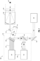
- FIG. 1 is a perspective section view of an example of an adaptive optics (AO) system 100.
- AO adaptive optics
- An AO system 104 of the system 100 is configured to correct these distortions (also known as phase aberrations), using an electrooptical sensor 105 such as wavefront sensor or metric sensor.
- a wavefront sensor may measure wavefront aberrations of the received optical wave 102 after it is reflected by a deformable mirror 106, also known as residual phase aberrations.
- the deformable mirror 106 is incorporated into the AO system 104 for phase aberration compensation, and a controller 107 receives input signals 108 from the electrooptical sensor 105.
- the Shack-Hartmann sensor is one type of wavefront sensor that may be used for adaptive optics, although others may be implemented.
- the controller 107 calculates control voltages 121 based on the input signals 108 resulting in real-time reshaping of a surface of the deformable mirror 106 to optimally compensate the impact of wavefront aberrations of the optical wave 102and improve a desired quality of optical field characteristics registered by an optical sensor 109.
- optical field characteristics include sharpness of an image of the object 101, or laser power coupled into a fiber and registered by a photo-detector in laser-based optical receiver systems.
- One example of a deformable mirror that may be implemented in AO systems is described in U.S. Patent No. 7,967,456 entitled "Scalable Size Deformable Pocket Mirror with On-pocket Bimorph Actuator," which is incorporated by reference in its entirety.
- the AO system 104 may include a number of optical elements such as a beam splitter 110 that diverts a portion 111 of the received optical wave 102 to the electrooptical sensor 105, and optical elements used for reimaging and scaling in size of the receiver telescope input aperture (pupil) into both the deformable mirror 106 and the electrooptical sensor 105)
- optical elements may include, for example, a beam steering component 112, an off-axis mirror 113 and a reimaging lens 114 , and a mirror 122 as shown in Figure 1 .
- the optical elements of the AO system 104 including the deformable mirror 106, and the electrooptical sensor 105 may be carefully aligned and may be protected from impact of environmental factors (e.g., vibrations, thermal expansions, etc.). Since many adaptive optics systems include a significant number of optical elements, such adaptive optics systems are often bulky, heavy, expensive, difficult to align, operate and maintain.
- Figure 2 is a perspective section view of another example of an adaptive optics (AO) system 200.
- the system 200 may include a laser source with a beam forming optical system 115 generates a laser beam 116 that passes through a dichroic beam splitter 117 and is reflected by the deformable mirror 106 of the AO system 104.
- the optics 103 may be used to receive the optical wave 102 as well as transmit an outgoing laser beam 118.
- the deformable mirror 106 may introduce wavefront phase modulation u(r,t), that provides pre-compensation of phase aberrations of the outgoing laser beam 118 via sensing of the residual aberrations of the received optical wave 102 with the electrooptical sensor 105.
- separation of a relatively high-power transmitted and low-power received light coming from the object 101 or a remote laser transceiver may be achieved by using slightly different wavelengths for the outgoing and received optical waves.
- the dichroic beam splitter 117 redirects the received optical wave 102 to the electrooptical sensor 105, while the transmitted laser beam 116 passes through the dichroic beam splitter 117.
- this wavelength separation may be accomplished using an external laser illuminator operating at a wavelength ⁇ ILL that is slightly different from the wavelength of the transmitted high-energy laser (HEL) beam ⁇ HEL .
- wavelength separation may be achieved using remotely operating laser transceivers with laser sources having somewhat different wavelengths.
- the dichroic beam splitter 117 may be configured to reflect optical waves scattered off the material (processing light) within a selected wavelength band and transmit the main high-energy laser beam wavelength.
- the pre-compensation of the outgoing beam's phase aberration may be performed using optimization of a measured signal that is proportional to one or another received light characteristic (control metric), for example power within the receiver aperture (power-in-the-bucket metric, J PIB ), or power coupled into a fiber (power-in-the-fiber, J PIF ), or metrics based on different statistical characteristics of backscattered speckle field (speckle metrics).
- control metric for example power within the receiver aperture (power-in-the-bucket metric, J PIB ), or power coupled into a fiber (power-in-the-fiber, J PIF ), or metrics based on different statistical characteristics of backscattered speckle field (speckle metrics).
- control metric for example power within the receiver aperture (power-in-the-bucket metric, J PIB ), or power coupled into a fiber (power-in-the-fiber, J PIF ), or metrics based on different statistical characteristics of backscattered speckle field (speckle
- Figure 3 is a perspective section view of another example of an adaptive optics (AO) system 300.
- Figure 3 illustrates a metric optimization AO system that shares an optical train for both the transmitted and received light.
- the electrooptical sensor 105 may include a metric sensor 301 as shown, rather than a wavefront sensor.
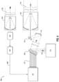
- Figure 4 is a perspective section view of another example of an adaptive optics (AO) system 400.
- the metric optimization-based AO system 400 may be simplified by separating transmitter and the receiver optics (e.g., telescopes).
- the system 400 may include the transmitter optics 103 and receiver optics 401.
- the received optical wave 102 may be measured by a photo-receiver 402 (e.g., photo-detector or photo-detector array), and processed by a control metric sensor 403.
- the computed control metric 404 may be sent to the controller 107.
- the controller 107 may compute control voltages 121 applied to the deformable mirror 106 using one or more metric optimization algorithms (e.g. the stochastic parallel gradient descent (SPGD)) to maximize or minimize the control metric 404.
- SPGD stochastic parallel gradient descent
- AO control architectures described with respect to Figures 1-4 may require installation and alignment of a large number of optical elements, resulting in substantial increase of the entire system size, weight and cost. This also makes the entire system highly sensitive to vibrations, "high g" and high-thermal gradient environmental factors. Accordingly, the disclosed embodiments include robust beam and wavefront control capabilities integrated directly to a DM thus addressing the challenges and drawbacks of the existing AO systems.
- on-mirror-integrated AO system both wavefront and control metric optimization types
- wavefront control and sensing capabilities are directly integrated into the specially designed adaptive optics embodiments.
- the described AO embodiments may be integrated, for example, on a on optical receiver or transmitter telescope primary mirror or secondary mirror.
- Such configurations may be referred to as on-mirror adaptive optics (OMAO) systems.
- OMAO on-mirror adaptive optics
- the OMAO system provides significantly simpler, robust and more compact AO solution compared with AO technologies described above and may be applied for instance to or fiber array-based laser beam transmitters, astronomical telescopes, free-space communication terminals and beam management systems used for laser material processing and additive manufacturing.
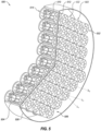
- FIG 5 is a perspective section view of an example of an OMAO component 500.
- Figure 6 is another perspective section view of the OMAO component 500.
- the OMAO component 500 may include multiple sub-apertures or pockets 502 (only three of which are labeled for simplicity).
- the pockets 502 may be formed in any suitable manner, for example, by making cuts in a substrate 504. Accordingly, the pockets 502 may be defined in the substrate 504.
- the substrate 504 may include a surface 506 which may be optically polished.
- a surface material may be deposited on the surface 506, and the surface material may be transparent or reflective, depending on an angle of incidence of light (see, for example, Figure 6 ).
- the substrate 504 may include glass and/or other appropriate materials.
- the surface 506 of the substrate 504 may include a dielectric layer 508 configured to transmit certain wavelengths of optical signals and reflect other wavelengths of optical signals. As shown, optical signals having wavelength ⁇ I are reflected by the dielectric layer 508 and optical signals having wavelength ⁇ 2 are transmitted by the dielectric layer 508 and may proceed into the pockets 502. Thus, the surface 506 may act as a dichroic mirror by reflecting desired certain wavelengths of optical signals and transmitting another desired wavelengths.
- Each of the pockets 502 may include wavefront or control metric signal sensing, controllable bending of the pocket front surface, and/or computation of control signals based on in-pocket measurements. Such aspects will be described in further detail below.
- the pockets 502 may include an in-pocket sensor 510 (e.g., an optical sensor, a wavefront sensor or a metric sensor), that measures optical signal characteristic of the light at wavelength ⁇ 2 that enters the pocket 502.
- the in-pocket sensor 510 may be a Shack-Hartman sensor, a power-in-the-bucket sensor, or a speckle-metric sensor, although other configurations may be implemented.
- the in-pocket sensor 510 may be used to detect aberrations or distortions in the optical signals which may be caused by the optical signals travelling through the atmosphere or other factors, or measure characteristics of light which are dependent on these aberrations.
- the pockets 502 may include one or more actuators 512.
- the actuator 512 may be configured to deform a portion of the surface 506 to compensate for aberrations or distortions (e.g., using signals detected by the in-pocket sensor 510).
- the actuator 512 may deform a portion of the surface 506 proximate to (or over) each of the corresponding one of the pockets 502.
- the deformation in the surface 506 caused by the actuator 512 may change the optical signals reflected by the dielectric layer 508 in a manner that compensates for the wavefront phase aberrations or distortions.
- the actuator 512 may be a multi-electrode bimorph element.
- the multi-electrode bimorph element may include a piezo-ceramic material bonded to a surface of each of the pockets 502, and actuated by applying control voltages to electrodes of the multi-electrode bimorph element. Additional aspects of deformable mirrors and associated actuators are described in further detail in U.S. Patent No. 7,967,456 entitled "Scalable Size Deformable Pocket Mirror with On-pocket Bimorph Actuator," which is incorporated by reference in its entirety.
- the actuator 512 may include any suitable aspects described in the above-mentioned document. However, the actuator 512 and associated deformable mirror surface 506 may include certain differences, as will be described in further detail below.
- Each of the pockets 502 may each include an electronic circuit or circuit board 514.
- the circuit board 514 may be included as part of the in-pocket sensor 510.
- the circuit board 514 may include various electronic components, for example, to sense aberrations or distortions in optical signals received at each corresponding one of the pockets 502.
- Figure 7 is a perspective view of a portion of one of the pockets 502 and Figure 8 is a section view of a portion of one of the pockets 502.
- the actuator 512 or a plurality of actuators may be electrically coupled to the circuit board 514 by electrical couplings 722.
- the electrical couplings 722 are wires extending between the circuit board 514 and the actuator 512, although any suitable electrical coupling may be implemented.
- the actuator 512 defines an opening 724 to permit optical signals to travel into the pocket 502 (e.g., through the dielectric layer 508 on the surface 506).
- the in-pocket sensor 510 may include one or more optical components 728 to transform optical signals travelling through the pocket 502, for example, a lenslet array corresponding to the Shack-Hartmann wavefront sensor, or a lens corresponding to a power-in-the-bucket metric sensor or speckle metric sensors.
- the circuit board 514 may include photo-detector or photo-detector array receiving the light transformed by optical component 728 of the in-pocket sensor 510 and provide electrical coupling of the corresponding in-pocket sensor 510 and the actuators 512.
- the circuit board 514 may receive electrical signals representative of the optical signals received at the pocket 502 from the in-pocket sensor 510.
- circuit board 514 may process the electrical signals to obtain control voltages sent to the actuators 512 to compensate for wavefront phase aberrations of the optical wave entering the pocket 502.
- the circuit board 514 may include control electronics configured to actuate or control the actuator 512 to deform the surface 506 in a manner to compensate for the aberrations.
- the circuit board 514 may include various electronic components which may be positioned on a circuit board (e.g., a printed circuit board or the like). As shown, the circuit board 514 may include a controller 716 and/or a receiver processor 718. The receiver processor 718 may be electrically coupled to a receiver or a receiver array 720, shown in Figure 8 . The receiver 720 may receive optical signals travelling through the pocket 502 and may generate electrical signals representative of the optical signals. Accordingly, the receiver 720 may be an optoelectronic component that converts optical signals to electrical signals.
- the controller 716 may be configured to receive electrical signals from the receiver 720, process these signals and send the processed electrical signals to actuate the actuator 512. Further, the receiver processor 718 and/or the controller 716 may detect aberrations or distortions in the optical signals travelling through the pocket 502 that are received at the receiver array 720. The controller 716 may then generate electrical signals to compensate for the aberrations or distortions and transmit the electrical signals to the actuator 512 (e.g. control voltages for the electrodes of the actuator 512).
- the actuator 512 includes a plurality of electrodes 726.
- the electrodes 726 are arranged in a circular pattern around the opening 724.
- the electrodes 726 may define the opening 724.
- the electrodes 726 may be configured to deform the deformable surface 506 when electrical signals (e.g., electrical currents or control voltages) are provided to the electrodes 726, for example, from the controller 716.
- the electrical signals may be provided to the electrodes 726 via the electrical couplings 722. Accordingly, as illustrated, one of the electrical couplings 722 may be included for each of the electrodes 726, although other configurations may be implemented.
- the in-pocket sensor 510 may include the optical component 728, the receiver 720 and the receiver processor 718, which may measure optical signals and transform them to electrical signals.
- the controller 716 may receive the electrical signals and generate control signals for the actuators 512 of the pocket 502.
- the in-pocket sensor 510 may include the optical component 728 or plurality of optical elements configured to focus, direct, or modulate the optical wave travelling through the pocket 502 and the receiver 720 configured to detect the optical signals after passing through the optical component 728.
- the optical component 728 may be supported by support members 730. As illustrated, the support members 730 affix the optical component 728 to the circuit board 514, although other configurations may be implemented. For example, the support members 730 may affix the optical component728 to the substrate 504. In other configurations, the support members 730 may not be included, for example, if the optical component 728 is formed in or affixed directly to the substrate 504.
- the optical signals with wavelength ⁇ 2 are transmitted through the dielectric layer 508 into the pocket 502, pass through the optical component 728 of the in-pocket sensor 510 and are received at the receiver 720, which converts the optical signals to electrical signals.
- the electrical signals are then processed by the receiver processor 718 and the controller 716 generates electrical signals to actuate the actuator 512 to compensate for aberrations or distortions in the optical signals with wavelength ⁇ 1 that is reflected by the dielectric layer 508 on the surface 506.
- the actuator 512 may deform the deformable surface 506 based on the electrical signals from the controller 716, which in turn changes the wavefront of the optical signals with wavelength ⁇ I which are reflected by the dielectric layer 508 on the surface 506.
- the actuator 512 deforms the deformable surface 506 proximate to or over the opening 724.
- the actuator 512 deforms the deformable surface 506 in an area in proximate vicinities of the electrodes 726.
- Such configurations may permit the in-pocket sensor 510 and the control electronics on the circuit board 514 to be incorporated in each of the pockets 502 individually. Additionally or alternatively, such configurations may provide additional degrees of freedom for compensation of atmospheric effects or other aberrations by providing sensing and control components as part of the pocket 502 itself.
- each of the pockets 502 includes a dedicated one of the controllers 716 and a dedicated one of the receiver processors 718.
- the controllers 716 and/or the receiver processors 718 may be positioned external or remote with respect to the pockets 502.
- a single controller and/or the receiver processor may operate with multiple pockets 502.
- one receiver processor may receive and process optical signals from multiple in-pocket sensors 510 of the multiple pockets 502.
- one controller may generate electrical signals for multiple actuators of multiple pockets.
- the controller may be communicatively coupled to the electrooptical sensor and the actuator, and the controller may be configured to generate control voltages based on signals received from the electrooptical sensor to deform a portion of the deformable surface proximate a corresponding pocket of the plurality of pockets.
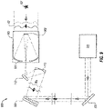
- Figure 9 is a perspective section view of another example of an on-mirror adaptive optics (OMAO) system 900.
- the illustrated example may include any suitable aspects described above with respect to Figures 1-3 .
- the OMAO system 900 also includes the OMAO component 500 described with respect to Figures 5-8 .
- the adaptive optical receiver configuration may be based on a phase-conjugate type control system architecture.
- the OMAO component 500 may provide measurements of phase aberrations of the received optical wave 102 inside each pocket 502 and may compute control voltages applied to the actuator 512 to compensate for these aberrations inside each pocket 502, for example, as illustrated in Figure 9 .
- the OMAO component 500 may be implemented instead of the AO system 104 described with respect to Figures 1-3 .
- integration of the OMAO component 500 results in significant simplification of the entire optical train, reduction of system weight, cost and robustness.
- the in-pocket sensor 510 may be represented by a Shack-Hartman, or any other wavefront sensor that provides measurements of wavefront aberrations.
- the optics 103 may include a primary mirror 901 and a secondary mirror 902.
- the OMAO component 500 may be integrated into the optics 103.
- the OMAO component 500 may be implemented in the primary mirror 901 or the secondary mirror 902 or both. Such configurations may result in an even more compact optical receiver system.
- Figure 10 is a perspective section view of another example of an on-mirror adaptive optics (OMAO) system 1000.
- Figure 10 illustrates the OMAO component 500 integrated into the optics 103, and in particular, in the receiver telescope primary mirror (corresponding to primary mirror 901 in Figure 9 ).
- the OMAO component 500 may be used to significantly simplify the transceiver OMAO system 200 described with respect to Figure 2 .
- Such configurations may be implemented in high energy laser (HEL) beam projection, laser communications, laser material processing and laser additive manufacturing
- the optics 103 may transmit a laser beam at wavelength ⁇ 1 that is reflected off dielectric layer 508 of the OMAO component 500.
- the optics 103 may also receive light at a different wavelength ⁇ 2 which originates from the object 101.
- the light may be received from another laser communication terminal.
- the light may be reflected off a target surface illuminated by a laser illuminator.
- a laser beacon light may be used for sensing turbulence-induced aberrations.
- a processing light generated by HEL beam may be used on a material to process the material.
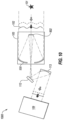
- Figure 11 is a perspective section view of another example of an on-mirror adaptive optics (OMAO) system 1100.
- OMAO on-mirror adaptive optics
- light at wavelength ⁇ 2 may enter the optics 103 and may pass through the dielectric layer 508 of the OMAO component 500 and may propagate into the in-pocket sensors 510.
- the in-pocket sensors 510 may be configured to measure wavefront aberrations light at wavelength ⁇ 2 entering the pockets 502 of the in phase-conjugate type control configurations of the OMAO component 500.
- the in-pocket sensors 510 may be configured to measure one or more received light characteristics (e.g., a control metric), in metric optimization type control configurations of the OMAO component 500.
- the control metric may include power within the receiver aperture (e.g., a power-in-the-bucket metric, J PIB ), or metrics based on different statistical characteristics of target backscattered light (e.g., speckle metrics) entering the optics 103.
- the OMAO system 1100 of Figure 11 may be further simplified via integration of the OMAO component 500 into the primary mirror 901, the secondary mirror 902 or both.
- each of the pockets 502 may include a dedicated one of the controllers 716 and a dedicated one of the receiver processors 718.
- the controllers 716 and/or the receiver processors 718 may be positioned external or remote with respect to the pockets 502.
- a single controller and/or the receiver processor may operate with multiple pockets 502.
- one receiver processor may receive and process optical signals from multiple in-pocket sensors 510 of multiple pockets 502.
- one controller may generate electrical signals for multiple actuators of multiple pockets.
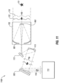
- FIG 12 is a perspective section view of another example of an on-mirror adaptive optics (OMAO) system 1200.
- the OMAO component 500 may be implemented to measure uncompensated (e.g., residual) phase aberrations or control metrics dependent on the residual phase aberrations of the received optical wave 102 inside each pocket 502.
- the OMAO component 500 may compute control voltages applied to the actuator 512 to compensate these residual phase aberrations inside the vicinity of each pocket 502 of the OMAO component 500.
- the received light at wavelength ⁇ 2 may be partially reflected from the dielectric layer 508 of the OMAO component 500.
- the dielectric layer 508 may be configured to be semitransparent for wavelength ⁇ 2 and highly reflective for wavelength ⁇ 1 .
- the optical wave 102 with externally aberrated phase ⁇ ( r , t ) may be received by the optics 103.
- the deformable surface 506 of the OMAO component 500 may provide additional phase modulation u(r,t), (e.g., controllable wavefront phase modulation).
- An optical wave 1204 may be reflected by the dichroic mirror 1202 and may propagate back to the OMAO component 500 and may enter one or more of the pockets 502.
- the corresponding controller 716 may be configured to mitigate the phase error ⁇ ( r , t ) within each pocket using one or more phase conjugation or metric optimization control algorithms.
- the in-pocket sensor 510 may be configured to measure characteristics (e.g., wavefront aberrations and/or control metrics) of the optical wave 1201 that is reflected from both the OMAO 500 and the dichroic mirror 1202, and to mitigate potential negative impacts of a portion of the received optical wave 1203 that enters the pockets 502 prior to reflection by the OMAO component 500. This may be achieved, for example, by using difference in incidence angles of the optical waves 1203 and 1201. The use of the angle of incidence as a discriminator may be achieved by any suitable configuration. For example, via incorporation of angular selective diffractive optics or holographic element into each pocket 502.
- characteristics e.g., wavefront aberrations and/or control metrics
- the pocket mirror array geometry may match the fiber-collimator array, so that each optical signal transmitted by the fiber array sub-aperture beam (beamlet) enters the corresponding pocket region of the OMAO component 500, and is reflected from the window of the pocket 502.
- the OMAO component 500 may provide enhancement of wavefront aberration capabilities of fiber array systems by providing wavefront aberration pre-compensation within each sub-aperture.
Landscapes
- Physics & Mathematics (AREA)
- General Physics & Mathematics (AREA)
- Optics & Photonics (AREA)
- Mechanical Light Control Or Optical Switches (AREA)
- Mounting And Adjusting Of Optical Elements (AREA)
- Micromachines (AREA)
- Spectroscopy & Molecular Physics (AREA)
Applications Claiming Priority (1)
| Application Number | Priority Date | Filing Date | Title |
|---|---|---|---|
| US17/385,474 US12117603B2 (en) | 2021-07-26 | 2021-07-26 | On-mirror integrated adaptive optics |
Publications (2)
| Publication Number | Publication Date |
|---|---|
| EP4124899A2 true EP4124899A2 (de) | 2023-02-01 |
| EP4124899A3 EP4124899A3 (de) | 2023-03-22 |
Family
ID=82214158
Family Applications (1)
| Application Number | Title | Priority Date | Filing Date |
|---|---|---|---|
| EP22180412.3A Pending EP4124899A3 (de) | 2021-07-26 | 2022-06-22 | Integrierte adaptive optik auf spiegeln |
Country Status (4)
| Country | Link |
|---|---|
| US (2) | US12117603B2 (de) |
| EP (1) | EP4124899A3 (de) |
| CN (1) | CN115685597A (de) |
| AU (1) | AU2022205215A1 (de) |
Cited By (1)
| Publication number | Priority date | Publication date | Assignee | Title |
|---|---|---|---|---|
| KR20240146975A (ko) * | 2023-03-30 | 2024-10-08 | 한국원자력연구원 | 저전력 레이저 스캐닝 시스템 및 방법 |
Families Citing this family (1)
| Publication number | Priority date | Publication date | Assignee | Title |
|---|---|---|---|---|
| EP4459895A1 (de) * | 2023-05-03 | 2024-11-06 | Aalyria Technologies, Inc. | Hybrides adaptives optisches system für optische freiraumkommunikation |
Citations (1)
| Publication number | Priority date | Publication date | Assignee | Title |
|---|---|---|---|---|
| US7967456B2 (en) | 2007-11-02 | 2011-06-28 | The United States Of America As Represented By The Secretary Of The Army | Scalable size deformable pocket mirror with on-pocket bimorph actuator |
Family Cites Families (4)
| Publication number | Priority date | Publication date | Assignee | Title |
|---|---|---|---|---|
| US6911637B1 (en) | 2002-05-23 | 2005-06-28 | The United States Of America As Represented By The Secretary Of The Army | Wavefront phase sensors using optically or electrically controlled phase spatial light modulators |
| EP2189769A1 (de) | 2008-11-19 | 2010-05-26 | BAE Systems PLC | Spiegelstruktur |
| US20130215527A1 (en) | 2012-02-17 | 2013-08-22 | Leonid A. Beresnev | Optically un-obscured controllable mirror for high-speed beam steering and phase aberration compensation |
| US10630043B1 (en) | 2019-05-14 | 2020-04-21 | Ii-Vi Delaware, Inc. | Methods and devices for laser beam parameters sensing and control with fiber-tip integrated systems |
-
2021
- 2021-07-26 US US17/385,474 patent/US12117603B2/en active Active
-
2022
- 2022-06-22 EP EP22180412.3A patent/EP4124899A3/de active Pending
- 2022-07-13 AU AU2022205215A patent/AU2022205215A1/en active Pending
- 2022-07-22 CN CN202210865853.6A patent/CN115685597A/zh active Pending
-
2024
- 2024-09-16 US US18/886,080 patent/US20250004266A1/en active Pending
Patent Citations (1)
| Publication number | Priority date | Publication date | Assignee | Title |
|---|---|---|---|---|
| US7967456B2 (en) | 2007-11-02 | 2011-06-28 | The United States Of America As Represented By The Secretary Of The Army | Scalable size deformable pocket mirror with on-pocket bimorph actuator |
Cited By (1)
| Publication number | Priority date | Publication date | Assignee | Title |
|---|---|---|---|---|
| KR20240146975A (ko) * | 2023-03-30 | 2024-10-08 | 한국원자력연구원 | 저전력 레이저 스캐닝 시스템 및 방법 |
Also Published As
| Publication number | Publication date |
|---|---|
| AU2022205215A1 (en) | 2023-02-09 |
| US20250004266A1 (en) | 2025-01-02 |
| US20230025437A1 (en) | 2023-01-26 |
| EP4124899A3 (de) | 2023-03-22 |
| CN115685597A (zh) | 2023-02-03 |
| US12117603B2 (en) | 2024-10-15 |
Similar Documents
| Publication | Publication Date | Title |
|---|---|---|
| US20250004266A1 (en) | On-mirror integrated adaptive optics | |
| EP3465272B1 (de) | Hochleistungstrahlungsdirektor für hochleistungslasersysteme und andere systeme | |
| US11909439B2 (en) | Wavefront sensor with inner detector and outer detector | |
| JPH10503300A (ja) | 適応光学モジュール | |
| US6911637B1 (en) | Wavefront phase sensors using optically or electrically controlled phase spatial light modulators | |
| US11652548B1 (en) | Free space optical communication terminal with chromatic Risley prism pair | |
| US20220085885A1 (en) | Setup for Receiving an Optical Data Signal | |
| US11777599B2 (en) | Free space optical communication terminal with rotatable dispersive optical component | |
| KR20040010780A (ko) | 대기 광학 데이터 전송 시스템 | |
| EP0977070B1 (de) | Teleskop mit gemeinsamem optischem Weg für ein optisches Kommunikationsendgerät | |
| WO2008097302A1 (en) | Common-aperture optical system incorporating a light sensor and a light source | |
| US8519315B2 (en) | Mirror structure having a fourier lens disposed between a reflective surface and an integrated optical sensor | |
| JP2003124890A (ja) | 自由空間光通信システム内の光信号波面の歪みを矯正する方法および装置 | |
| US10567654B2 (en) | Automatic structurally induced line of sight jitter compensation for electro-optical/infrared turret system | |
| US20150301321A1 (en) | Modified Schmidt-Cassegrain Telescope For Use In A Free-Space Optical Communications System | |
| CN209201088U (zh) | 双向校正共孔径收发的自适应光学激光通信光学终端 | |
| JP2001203641A (ja) | 空間光伝送装置 | |
| EP4387159A1 (de) | Qkd-endgerät, qkd-system und verfahren zur quantenkommunikation | |
| KR100615054B1 (ko) | 형상가변거울을 이용한 파면에러 보정장치 | |
| US20130063804A1 (en) | Digital binary mems wavefront control | |
| EP2189769A1 (de) | Spiegelstruktur | |
| CN209358549U (zh) | 双向同频段自适应光学激光通信光学终端 | |
| CN114928405B (zh) | 一种激光通信光信号接收系统及其工作方法 | |
| JP4675870B2 (ja) | 光制御型ビーム形成回路 | |
| WO2025252620A1 (en) | Depth sensing system, illumination unit and matching optics |
Legal Events
| Date | Code | Title | Description |
|---|---|---|---|
| PUAI | Public reference made under article 153(3) epc to a published international application that has entered the european phase |
Free format text: ORIGINAL CODE: 0009012 |
|
| STAA | Information on the status of an ep patent application or granted ep patent |
Free format text: STATUS: THE APPLICATION HAS BEEN PUBLISHED |
|
| AK | Designated contracting states |
Kind code of ref document: A2 Designated state(s): AL AT BE BG CH CY CZ DE DK EE ES FI FR GB GR HR HU IE IS IT LI LT LU LV MC MK MT NL NO PL PT RO RS SE SI SK SM TR |
|
| PUAL | Search report despatched |
Free format text: ORIGINAL CODE: 0009013 |
|
| AK | Designated contracting states |
Kind code of ref document: A3 Designated state(s): AL AT BE BG CH CY CZ DE DK EE ES FI FR GB GR HR HU IE IS IT LI LT LU LV MC MK MT NL NO PL PT RO RS SE SI SK SM TR |
|
| RIC1 | Information provided on ipc code assigned before grant |
Ipc: G02B 26/08 20060101AFI20230210BHEP |
|
| P01 | Opt-out of the competence of the unified patent court (upc) registered |
Effective date: 20230515 |
|
| STAA | Information on the status of an ep patent application or granted ep patent |
Free format text: STATUS: REQUEST FOR EXAMINATION WAS MADE |
|
| 17P | Request for examination filed |
Effective date: 20230810 |
|
| RBV | Designated contracting states (corrected) |
Designated state(s): AL AT BE BG CH CY CZ DE DK EE ES FI FR GB GR HR HU IE IS IT LI LT LU LV MC MK MT NL NO PL PT RO RS SE SI SK SM TR |
|
| STAA | Information on the status of an ep patent application or granted ep patent |
Free format text: STATUS: EXAMINATION IS IN PROGRESS |
|
| 17Q | First examination report despatched |
Effective date: 20250515 |
|
| RAP1 | Party data changed (applicant data changed or rights of an application transferred) |
Owner name: COHERENT AEROSPACE & DEFENSE, INC. |