EP4123335A1 - Scanning device and distance measuring device - Google Patents
Scanning device and distance measuring device Download PDFInfo
- Publication number
- EP4123335A1 EP4123335A1 EP21770776.9A EP21770776A EP4123335A1 EP 4123335 A1 EP4123335 A1 EP 4123335A1 EP 21770776 A EP21770776 A EP 21770776A EP 4123335 A1 EP4123335 A1 EP 4123335A1
- Authority
- EP
- European Patent Office
- Prior art keywords
- unit
- electromagnetic wave
- scanning
- electromagnetic waves
- scanning device
- Prior art date
- Legal status (The legal status is an assumption and is not a legal conclusion. Google has not performed a legal analysis and makes no representation as to the accuracy of the status listed.)
- Granted
Links
Images




Classifications
-
- G—PHYSICS
- G01—MEASURING; TESTING
- G01S—RADIO DIRECTION-FINDING; RADIO NAVIGATION; DETERMINING DISTANCE OR VELOCITY BY USE OF RADIO WAVES; LOCATING OR PRESENCE-DETECTING BY USE OF THE REFLECTION OR RERADIATION OF RADIO WAVES; ANALOGOUS ARRANGEMENTS USING OTHER WAVES
- G01S7/00—Details of systems according to groups G01S13/00, G01S15/00, G01S17/00
- G01S7/48—Details of systems according to groups G01S13/00, G01S15/00, G01S17/00 of systems according to group G01S17/00
- G01S7/481—Constructional features, e.g. arrangements of optical elements
- G01S7/4817—Constructional features, e.g. arrangements of optical elements relating to scanning
-
- G—PHYSICS
- G01—MEASURING; TESTING
- G01S—RADIO DIRECTION-FINDING; RADIO NAVIGATION; DETERMINING DISTANCE OR VELOCITY BY USE OF RADIO WAVES; LOCATING OR PRESENCE-DETECTING BY USE OF THE REFLECTION OR RERADIATION OF RADIO WAVES; ANALOGOUS ARRANGEMENTS USING OTHER WAVES
- G01S7/00—Details of systems according to groups G01S13/00, G01S15/00, G01S17/00
- G01S7/48—Details of systems according to groups G01S13/00, G01S15/00, G01S17/00 of systems according to group G01S17/00
- G01S7/481—Constructional features, e.g. arrangements of optical elements
- G01S7/4814—Constructional features, e.g. arrangements of optical elements of transmitters alone
- G01S7/4815—Constructional features, e.g. arrangements of optical elements of transmitters alone using multiple transmitters
-
- G—PHYSICS
- G01—MEASURING; TESTING
- G01S—RADIO DIRECTION-FINDING; RADIO NAVIGATION; DETERMINING DISTANCE OR VELOCITY BY USE OF RADIO WAVES; LOCATING OR PRESENCE-DETECTING BY USE OF THE REFLECTION OR RERADIATION OF RADIO WAVES; ANALOGOUS ARRANGEMENTS USING OTHER WAVES
- G01S7/00—Details of systems according to groups G01S13/00, G01S15/00, G01S17/00
- G01S7/48—Details of systems according to groups G01S13/00, G01S15/00, G01S17/00 of systems according to group G01S17/00
- G01S7/481—Constructional features, e.g. arrangements of optical elements
- G01S7/4816—Constructional features, e.g. arrangements of optical elements of receivers alone
-
- G—PHYSICS
- G01—MEASURING; TESTING
- G01S—RADIO DIRECTION-FINDING; RADIO NAVIGATION; DETERMINING DISTANCE OR VELOCITY BY USE OF RADIO WAVES; LOCATING OR PRESENCE-DETECTING BY USE OF THE REFLECTION OR RERADIATION OF RADIO WAVES; ANALOGOUS ARRANGEMENTS USING OTHER WAVES
- G01S7/00—Details of systems according to groups G01S13/00, G01S15/00, G01S17/00
- G01S7/48—Details of systems according to groups G01S13/00, G01S15/00, G01S17/00 of systems according to group G01S17/00
- G01S7/481—Constructional features, e.g. arrangements of optical elements
- G01S7/4818—Constructional features, e.g. arrangements of optical elements using optical fibres
-
- G—PHYSICS
- G02—OPTICS
- G02B—OPTICAL ELEMENTS, SYSTEMS OR APPARATUS
- G02B26/00—Optical devices or arrangements for the control of light using movable or deformable optical elements
- G02B26/08—Optical devices or arrangements for the control of light using movable or deformable optical elements for controlling the direction of light
- G02B26/10—Scanning systems
- G02B26/101—Scanning systems with both horizontal and vertical deflecting means, e.g. raster or XY scanners
-
- G—PHYSICS
- G02—OPTICS
- G02B—OPTICAL ELEMENTS, SYSTEMS OR APPARATUS
- G02B26/00—Optical devices or arrangements for the control of light using movable or deformable optical elements
- G02B26/08—Optical devices or arrangements for the control of light using movable or deformable optical elements for controlling the direction of light
- G02B26/10—Scanning systems
- G02B26/105—Scanning systems with one or more pivoting mirrors or galvano-mirrors
Definitions
- the present invention relates to a scanning device and a distance measuring device.
- a known device uses a laser radar to measure the position of an object within an image captured by an infrared camera (for example, refer to Patent Literature 1).
- a known scanning device deflects electromagnetic waves radiated from an irradiation unit by reflecting the waves with a reflecting mirror (for example, refer to Patent Literature 2).
- a scanning device includes a first irradiation unit, a second irradiation unit, a scanning unit, a waveguide unit, and a detection unit.
- the first irradiation unit is configured to radiate a first electromagnetic wave for scanning an object of interest.
- the second irradiation unit is configured to radiate a second electromagnetic wave.
- the scanning unit is configured to deflect and output the first electromagnetic wave radiated by the first irradiation unit and the second electromagnetic wave radiated by the second irradiation unit.
- the waveguide unit is configured to guide at least part of the second electromagnetic wave output by the scanning unit in a different direction from the first electromagnetic wave.
- the detection unit is configured to detect the second electromagnetic wave guided in the different direction from the first electromagnetic wave by the waveguide unit.
- a distance measuring device includes an operation device according to an embodiment.
- a scanning device includes a scanning unit, a waveguide unit, and a detection unit.
- the scanning unit is configured to deflect an electromagnetic wave entered.
- the waveguide unit is configured to separate the electromagnetic wave deflected by the scanning unit into a first electromagnetic wave and a second electromagnetic wave.
- the detection unit is configured to detect the second electromagnetic wave separated by the waveguide unit.
- the detection unit is disposed at a position outside the irradiation range of the first electromagnetic wave separated by the waveguide unit from the electromagnetic wave deflected by the scanning unit.
- a solution of the present disclosure is described in the form of a scanning device and a distance measuring device.
- the present disclosure can also be realized in forms including these devices and furthermore can be realized as a method, a program, or a storage medium recording a program substantially equivalent to these devices, and note that the scope of the present disclosure includes these forms as well.
- a reflecting mirror that deflects the electromagnetic waves is rotationally driven using, for example, an electromechanical conversion element based on micromachining technologies.
- a sensor such as a photodiode that detects electromagnetic waves deflected by the reflecting mirror may be used to detect the swing angle of the rotationally driven reflecting mirror.
- Such a sensor needs to be disposed at a position where electromagnetic waves deflected by the reflecting mirror can be detected by the sensor. Therefore, in a scanning device that performs scanning using electromagnetic waves, the range across which electromagnetic waves are radiated (scannable range) may be restricted depending on the position at which the sensor for detecting the swing angle of the reflecting mirror is disposed.
- the present disclosure provides a scanning device and a distance measuring device that can secure or expand a range to be irradiated with electromagnetic waves.
- a scanning device and a distance measuring device can secure or expand a range to be irradiated with electromagnetic waves.
- a scanning device is described below while referring to the drawings.
- FIGs. 1 to 3 illustrate the schematic configuration of a scanning device according to an embodiment.
- FIG. 1 is a perspective view illustrating the schematic configuration of the scanning device according to an embodiment.
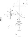
- FIG. 2 is a view (plan view) of the schematic configuration of the scanning device illustrated in FIG. 1 from a different perspective from FIG. 1 .
- FIG. 3 illustrates the schematic configuration (right side view) of the scanning device illustrated in FIGs. 1 and 2 from a different perspective from FIGs. 1 and 2 .
- a positive X-axis direction corresponds to a rightward direction in FIG. 2 and a negative X-axis direction corresponds to a leftward direction in FIG. 2 .
- a positive Y-axis direction corresponds to a rearward direction in FIG. 1 (the direction of travel of electromagnetic waves reflected by a reflecting mirror) and a negative Y-axis direction corresponds to a forward direction in FIG. 1 .
- a positive Z-axis direction corresponds to an upward direction in FIG. 3 and a negative Z-axis direction corresponds to a downward direction in FIG. 3 .
- a scanning device 1 may include a substrate 10, a first detection unit 21, a second detection unit 22, a first irradiation unit 31, a second irradiation unit 32, a combining unit 40, a scanning unit 50, a waveguide unit 60, and an emitting unit 70.
- the scanning device 1 may include all of the functional units described above, may include functional units other than those described above, and does not necessarily include some of the functional units described above.
- the functional units described above are separated from each other to a sufficient degree to allow convenience of explanation.
- the functional units included in the scanning device 1 may be more densely arranged than is illustrated in FIGs. 1 to 3 .
- the functional units of the scanning device 1 may be disposed to be compactly configured to fit within an area of around a few square centimeters.
- arrows projecting from the individual functional blocks represent beams of electromagnetic waves.
- the functional blocks illustrated in FIGs. 1 to 3 may be connected to various functional units that control and/or drive the functional blocks in a wired or wireless manner as appropriate. In FIGs. 1 to 3 , for convenience of explanation, the various functional units that control and/or drive the functional blocks are omitted. Furthermore, the functional blocks illustrated in FIGs. 1 to 3 may be connected to functional units that supply power to the functional blocks as appropriate. In FIGs. 1 to 3 , the functional units that supply power to the functional blocks are omitted for convenience of explanation.
- the functional blocks illustrated in FIGs. 1 to 3 may be fixed and/or positioned at the positions illustrated in the figures as appropriate. In FIGs. 1 to 3 , various components used to fix in place and/or position the functional blocks are omitted for convenience of explanation.
- the scanning device 1 can radiate electromagnetic waves and deflect and output the radiated electromagnetic waves, as further described below. At least a portion of the electromagnetic waves deflected by the scanning device 1 may be reflected by a predetermined object of interest (such as an object). The electromagnetic waves (reflected waves) reflected by the predetermined object or the like may be detected by, for example, an electromagnetic wave detection device.
- the scanning device 1 of an embodiment and the electromagnetic wave detection device as described above may be included in an information acquisition system (for example, a distance measuring device) according to an embodiment.
- the distance measuring device may include the scanning device 1 according to an embodiment and may measure the distance to an object of interest.
- an information acquisition system may, for example, employ a light detection and ranging, laser image detection and ranging (LIDAR) technology used for "light detection and distance measurement” or "laser image detection and distance measurement”.
- LIDAR laser image detection and ranging
- the distance to a relatively distant object and/or a property of the object may be analyzed by measuring scattered light with respect to pulsed laser radiation.
- the substrate 10 may be a substrate in which the X-axis direction is a longitudinal direction thereof and the Y-axis direction is a lateral direction thereof.
- the substrate 10 may be a substrate having a thickness in the Z-axis direction.
- the substrate 10 may be fixed in place in the scanning device 1 to be parallel to the XY plane.
- the substrate 10 has a first surface 10A and a second surface 10B.
- the first surface 10A of the substrate 10 may be the surface of the substrate 10 facing in the negative Z-axis direction, i.e., the downward facing surface of the substrate 10.
- the second surface 10B of the substrate 10 may be the surface of the substrate 10 that facing in the positive Z-axis direction, i.e., the upward facing surface of the substrate 10.
- the substrate 10 may have the first surface 10A and the second surface 10B on the opposite side from the first surface 10A.
- the substrate 10 may be, for example, a plate-shaped member made of an insulator.
- the substrate 10 may be a plate-shaped member made of an insulator with conductor wiring on the surface of or inside the plate-shaped member.
- the substrate 10 may be a printed wiring board (PWB) in a state prior to disposing electronic components attached thereto.
- the substrate 10 may be a printed circuit board (PCB) in which electronic components have soldered to the printed circuit board so that the printed circuit board can operate as an electronic circuit.
- the substrate 10 may be any of various substrates defined in JIS standard JISC5603 or IEC60194.
- the substrate 10 may be a printed circuit, printed wiring, a printed circuit board, a printed circuit assembly, a printed wiring board, or a printed board.
- the substrate 10 is a rigid substrate.
- the substrate 10 is not limited to being a rigid substrate and may be, for example, a rigid-flexible substrate (flex-rigid) or a flexible substrate (FPC).
- flex-rigid rigid-flexible substrate
- FPC flexible substrate
- the substrate 10 may include a passage portion 12.
- the passage portion 12 of the substrate 10 is further described below.
- the first and second detection units 21 and 22 may be provided on the first surface 10A of the substrate 10, i.e., the downward facing surface of the substrate 10, as illustrated in FIG. 3 . Since FIG. 3 illustrates the right side of the scanning device 1, only the second detection unit 22 is illustrated, and the first detection unit 21 is not illustrated. In FIGs. 1 and 2 , the first and second detection units 21 and 22 are located at positions where the first and second detection units 21 and 22 cannot be seen and are therefore illustrated using dashed lines.
- the first detection unit 21 and the second detection unit 22 may detect predetermined electromagnetic waves.
- the first detection unit 21 may detect, for example, visible light incident on the first detection unit 21.
- the second detection unit 22 may detect, for example, visible light incident on the second detection unit 22.
- the detection surfaces at which electromagnetic waves are detected by the first detection unit 21 and the second detection unit 22 may be surfaces facing in the negative Z-axis direction, i.e., the downward facing surfaces of the first detection unit 21 and the second detection unit 22.
- the first detection unit 21 may detect, for example, visible light VL (hereinafter, also referred to as electromagnetic waves VL) incident on the first detection unit 21.
- the second detection unit 22 may detect, for example, visible light VL incident on the second detection unit 22.
- the first detection unit 21 and the second detection unit 22 may be, for example, photodiodes (PDs), which are semiconductor diodes functioning as photodetectors. As described below, the first detection unit 21 and the second detection unit 22 may each detect electromagnetic waves that are scanned (deflected) by the scanning unit 50. Thus, the first detection unit 21, which detects electromagnetic waves, and the second detection unit 22, which detects electromagnetic waves, may be provided on the first surface 10A of the substrate 10. The positions where the first detection unit 21 and the second detection unit 22 are provided on the first surface 10A of the substrate 10 are further described below.
- PDs photodiodes
- the first detection unit 21 and the second detection unit 22 are provided as two detection units on the substrate 10 illustrated in FIGs. 1 to 3 .
- the first detection unit 21 and the second detection unit 22 may simply be referred to as “detection unit 20" or “detection units 20".
- the number of detection units provided on the substrate 10 is not limited to two.
- the substrate 10 may be provided with only one detection unit 20, such as the first detection unit 21 or the second detection unit 22.
- the substrate 10 may be provided with three or more detection units 20, each being the first detection unit 21 or the second detection unit 22.
- the detection units 20 may each include a photodiode that detects the visible light VL radiated by the second irradiation unit 32.
- the first irradiation unit 31 may radiate predetermined first electromagnetic waves.
- the first irradiation unit 31 may radiate, for example, infrared radiation as electromagnetic waves for scanning a predetermined object of interest.
- the direction in which the first irradiation unit 31 radiates the first electromagnetic waves may be, for example, the positive X-axis direction, i.e., to the right in FIG. 2 .
- the first irradiation unit 31 may radiate the infrared radiation IR (hereinafter also referred to as electromagnetic waves IR), for example, in the positive X-axis direction toward the combining unit 40. Therefore, the first irradiation unit 31 may be positioned and/or fixed in place so that the infrared radiation IR radiated by the first irradiation unit 31 is incident on the combining unit 40.
- the first irradiation unit 31 may be a laser diode (LD) or a diode laser, which is a semiconductor laser that functions as a laser using semiconductor recombination emission, for example.
- the first irradiation unit 31 may include a laser diode that radiates infrared radiation as the first electromagnetic waves.
- the first irradiation unit 31 may, for example, radiate pulsed electromagnetic waves.
- the first irradiation unit 31 may be an array including, for example, a plurality of laser diodes.
- the second irradiation unit 32 may radiate predetermined second electromagnetic waves.
- the second irradiation unit 32 may radiate visible light, for example, as electromagnetic waves for detecting the irradiation direction of the electromagnetic waves used for scanning (i.e., the swing angle of the reflecting mirror).
- the direction in which the second irradiation unit 32 radiates the second electromagnetic waves may be, for example, the positive Y-axis direction, i.e., the rearward direction in FIG. 1 .
- the second irradiation unit 32 may radiate the visible light VL, for example, in the positive Y-axis direction toward the combining unit 40.
- the second irradiation unit 32 may be positioned and/or fixed in place so that the visible light VL radiated by the second irradiation unit 32 is incident on the combining unit 40.
- the visible light VL may be red, for example, to improve visibility.
- the second irradiation unit 32 may be, for example, a laser diode (LD) or a diode laser, which is a semiconductor laser that functions as a laser using semiconductor recombination emission.
- the second irradiation unit 32 may be a light-emitting diode (LED) that radiates visible light.
- the second irradiation unit 32 may include a laser diode that radiates visible light as the second electromagnetic waves.
- the second irradiation unit 32 may, for example, radiate steady light.
- the combining unit 40 outputs, in a predetermined direction, two sets of electromagnetic waves input from different directions. Specifically, the combining unit 40 may combine the first electromagnetic waves radiated from the first irradiation unit 31 and the second electromagnetic waves radiated from the second irradiation unit 32 by matching their optical axes. The combining unit 40 may then output the combined electromagnetic waves toward the scanning unit 50. As illustrated in FIGs. 1 and 2 , the combining unit 40 may combine the infrared radiation IR input from the first irradiation unit 31 and the visible light VL input from the second irradiation unit 32 and output the combined electromagnetic waves IR and VL to the scanning unit 50.
- the combining unit 40 may be positioned and/or fixed in place so that the infrared radiation IR radiated from the first irradiation unit 31 is incident thereon.
- the combining unit 40 may be positioned and/or fixed in place so that the visible light VL radiated from the second irradiation unit 32 is incident thereon.
- the combining unit 40 may be positioned so that the first electromagnetic waves (infrared radiation IR) radiated by the first irradiation unit 31 and the second electromagnetic waves (visible light VL) radiated by the second irradiation unit 32 are incident thereon.
- the combining unit 40 may be positioned and/or fixed in place so that the combined electromagnetic waves IR and VL are incident on the scanning unit 50.
- the combining unit 40 may include, for example, a prism or a cold mirror. Any configuration may be adopted for the combining unit 40 as long as the combining unit 40 is able to match the directions of travel of the first electromagnetic waves radiated from the first irradiation unit 31 and the second electromagnetic waves radiated from the second irradiation unit 32 and output the resulting electromagnetic waves in a predetermined direction.
- the combining unit 40 may have a function of matching the direction of travel of the first electromagnetic waves (infrared radiation IR) and the direction of travel of the second electromagnetic waves (visible light VL) with each other.
- the combining unit 40 may combine the first electromagnetic waves radiated from the first irradiation unit 31 and the second electromagnetic waves radiated from the second irradiation unit 32 as coaxial electromagnetic waves and then output the combined electromagnetic waves as coaxial electromagnetic waves in a predetermined direction.
- the combining unit 40 does not necessarily combine the first electromagnetic waves radiated from the first irradiation unit 31 and the second electromagnetic waves radiated from the second irradiation unit 32 into coaxial electromagnetic waves. However, it is desirable that the directions of travel of the first electromagnetic waves and the second electromagnetic waves match. In FIGs.
- the combining unit 40 combines electromagnetic waves radiated from mutually perpendicular directions such as the first electromagnetic waves radiated from the first irradiation unit 31 and the second electromagnetic waves radiated from the second irradiation unit 32.
- the combining unit 40 may transmit the first electromagnetic waves radiated from the first irradiation unit 31 and reflect the second electromagnetic waves radiated from the second irradiation unit 32 in the direction in which the first electromagnetic waves are transmitted.
- the first and second electromagnetic waves are combined in the combining unit 40 such that their directions of travel match.
- the combining unit 40 outputs the combined electromagnetic waves in the same direction as the first electromagnetic waves radiated from the first irradiation unit 31, i.e., in the positive X-axis direction. It is acceptable that the combining unit 40 output the first electromagnetic waves radiated from the first irradiation unit 31 toward the scanning unit 50 and also output the second electromagnetic waves radiated from the second irradiation unit 32 toward the scanning unit 50, and the directions of travel of the first and second electromagnetic waves do not necessarily need to match.
- the scanning unit 50 deflects and then outputs the electromagnetic waves input from the combining unit 40.
- the scanning unit 50 may include, for example, a reflecting mirror that deflects the incident electromagnetic waves.
- the reflecting mirror of the scanning unit 50 may be, for example, a micro electro mechanical systems (MEMS) mirror, a polygon mirror, or galvano mirror.
- MEMS micro electro mechanical systems
- the reflecting mirror of the scanning unit 50 is described below as including a MEMS mirror.
- the scanning unit 50 has a rotation axis that is parallel to the Z-axis and the scanning unit 50 rotates around this axis in a lateral direction.
- the rotational motion is not necessarily circumferential motion.
- the rotational motion may be oscillating motion that includes, as part thereof, rotational motion (for example, less than one complete revolution).
- the scanning unit 50 may rotationally move in the directions indicated by arrow S.
- the scanning unit 50 may deflect the electromagnetic waves IR and VL input from the combining unit 40 toward, for example, the waveguide unit 60 by rotationally moving as indicated by the arrow S.
- the paths of the electromagnetic waves IR and VL deflected by the scanning unit 50 may lie on a plane parallel to the XY plane.
- the scanning unit 50 may be positioned so that the electromagnetic waves IR and VL radiated from the combining unit 40 are incident thereon.
- the scanning unit 50 may also be positioned such that the electromagnetic waves IR and VL deflected by the scanning unit 50 are incident on the waveguide unit 60.
- the scanning unit 50 may change and then output the first electromagnetic waves (infrared radiation IR) radiated by the first irradiation unit 31 and the second electromagnetic waves (visible light VL) radiated by the second irradiation unit 32.
- the scanning unit 50 may scan the first electromagnetic waves (infrared radiation IR) and the second electromagnetic waves (visible light VL) output from the combining unit 40.
- the waveguide unit 60 may reflect visible light and allow infrared light to pass therethrough.
- the waveguide unit 60 allows the first electromagnetic waves (infrared radiation IR) radiated by the first irradiation unit 31 to pass therethrough and reflects the second electromagnetic waves (visible light VL) radiated by the second irradiation unit 32.
- the waveguide unit 60 may include, for example, a cold mirror.
- the waveguide unit 60 may allow the infrared radiation IR radiated by the first irradiation unit 31 to pass therethrough and reflect the visible light VL radiated by the second irradiation unit 32.
- the waveguide unit 60 may have any configuration as long as the waveguide unit 60 can allow the first electromagnetic waves radiated by the first irradiation unit 31 to pass therethrough and reflect the second electromagnetic waves radiated by the second irradiation unit 32.
- waveguide unit 60 allows the infrared radiation IR (or at least part of the infrared radiation IR) out of the electromagnetic waves IR and VL incident from scanning unit 50 to pass therethrough. As illustrated in FIGs. 1 to 3 , the waveguide unit 60 reflects the visible light VL (or at least part of the visible light VL) out of the electromagnetic waves IR and VL incident from the scanning unit 50.
- the waveguide unit 60 may be disposed to be inclined at a predetermined angle ⁇ from a plane parallel to the XY plane. Being inclined at the angle ⁇ allows the waveguide unit 60 to reflect, in the positive Z-axis direction, the visible light VL (or at least a portion of the electromagnetic waves VL) out of the electromagnetic waves IR and VL incident from the scanning unit 50.
- the waveguide unit 60 may guide at least a portion of the second electromagnetic waves (visible light VL), deflected by the scanning unit 50, in a different direction from the first electromagnetic waves (infrared radiation IR).
- the waveguide unit 60 may be positioned and/or fixed in place so that the electromagnetic waves IR and VL scanned (deflected) by the scanning unit 50 are incident thereon.
- the waveguide unit 60 may be positioned and/or fixed in place so that the second electromagnetic waves (visible light VL) reflected by the waveguide unit 60 are directed toward the substrate 10.
- the first and second detection units 21 and 22 are disposed on the first surface 10A of the substrate 10. Accordingly, when the waveguide unit 60 is properly positioned, the waveguide unit 60 can guide the electromagnetic waves VL scanned by the scanning unit 50 toward at least one out of the first detection unit 21 and the second detection unit 22.
- the detection unit 20 may detect the second electromagnetic waves VL, which are guided in a different direction from the first electromagnetic waves (infrared radiation IR) by the waveguide unit 60.
- the emitting unit 70 may emit from the scanning device 1 at least a portion of the first electromagnetic waves (infrared radiation IR) scanned by the scanning unit 50. More specifically, the emitting unit 70 may emit the first electromagnetic waves (infrared radiation IR) that have passed through the waveguide unit 60, out of the first electromagnetic waves (infrared radiation IR) and the second electromagnetic waves (visible light VL) scanned by the scanning unit 50.
- the emitting unit 70 may be made of, for example, glass or acrylic to allow the first electromagnetic waves (infrared radiation IR) to entirely pass through the emitting unit 70.
- the emitting unit 70 may allow at least a portion of the first electromagnetic waves (infrared radiation IR) to pass through the emitting unit 70 only at a part thereof from which the first electromagnetic waves are to be emitted. In this case, the emitting unit 70 does not allow at least a portion of the first electromagnetic waves to pass the emitting unit 70 in parts thereof other than the part thereof from which the first electromagnetic waves (infrared radiation IR) are to be emitted.
- the emitting unit 70 may emit the first electromagnetic waves (infrared radiation IR) output by the scanning unit 50.
- the waveguide unit 60 may be positioned on a path of the first electromagnetic waves (infrared radiation IR) output by the scanning unit 50. The path extends up to the emitting unit 70 through which the first electromagnetic waves are emitted.
- the infrared radiation IR radiated from the first irradiation unit 31 is deflected by the scanning unit 50.
- the infrared radiation IR deflected by the scanning unit 50 is emitted from the scanning device 1 after passing through the waveguide unit 60 and the emitting unit 70 and can then be used to scan objects and so forth in the surrounding area.
- the visible light VL radiated from the second irradiation unit 32 is deflected by the scanning unit 50 together with the infrared radiation IR radiated from the first irradiation unit 31.
- the visible light VL radiated from the second irradiation unit 32 is reflected by the waveguide unit 60 in the positive Z-axis direction after being deflected by the scanning unit 50.
- the visible light VL reflected by the waveguide unit 60 can be detected by the first detection unit 21 and/or the second detection unit 22 depending on the deflection direction of the visible light VL deflected by the scanning unit 50, which moves in a rotational manner. Therefore, the scanning device 1 can detect the irradiation direction of the infrared radiation IR by detecting the angle of rotation (swing angle) of the scanning unit 50.
- the scanning device 1 can cause the beams of visible light VL, out of the electromagnetic waves IR and VL scanned by the scanning unit 50, to be incident on the first detection unit 21 and/or the second detection unit 22.
- the scanning device 1 may store an angle detection table in which the angle of rotation of the reflecting mirror when the visible light VL reflected by the rotationally moving reflecting mirror is detected by the first detection unit 21 or the second detection unit 22 and the angle of rotation of the reflecting mirror with respect to the elapsed time from that state are associated with each other. In this way, the scanning device 1 can detect the angle of rotation of the scanning unit 50 (reflecting mirror) based on the elapsed time from respective timings at which the first detection unit 21 and the second detection unit 22 receive the light.
- the scanning device 1 can detect the irradiation direction of the infrared radiation IR.
- the scanning device 1 may include a controller (CPU), which is not illustrated, to perform processing for detecting the angle of rotation of the scanning unit 50.
- This controller may detect the state of the scanning unit 50 based on the detection of the second electromagnetic waves by the first detection unit 21 and/or the second detection unit 22.
- the scanning device 1 may include a controller that detects the state of the scanning unit 50 based on detection of the second electromagnetic waves by the first detection unit 21 and/or the second detection unit 22.
- the scanning device 1 can detect, in a direction different from the irradiation direction of the infrared radiation IR used for scanning, the visible light VL to determine the swing angle of the infrared radiation IR used for scanning.
- the detection unit for the visible light VL is not disposed in the irradiation range of the infrared radiation IR. Therefore, in the scanning device 1, a large scanning range can be set for scanning using the infrared radiation IR while reducing the size of the scanning device 1.
- the first detection unit 21 and the second detection unit 22 need to be disposed on the downwardfacing first surface 10A of the substrate 10 to detect the visible light VL, as illustrated in FIGs. 1 to 3 .
- the first detection unit 21 and the second detection unit 22 may be disposed at positions on the substrate 10 such that the first and second detection units 21 and 22 cannot be seen from the upper side.
- the first detection unit 21 and the second detection unit 22 need to be disposed at positions where the visible light VL scanned by the MEMS mirror of the scanning unit 50 is incident thereon.
- the first detection unit 21 and the second detection unit 22 need to be accurately positioned at positions where the visible light VL can be detected.
- accurate positioning due to dimensional and/or assembly tolerances of the components may or may not be guaranteed unless the positions of the first and second detection units 21 and 22 are adjusted during assembly.
- the positions of the first detection unit 21 and the second detection unit 22 may or may not be adjusted visually when adjusting the positions of the first detection unit 21 and the second detection unit 22 during assembly of the scanning device 1. In this case, the visual positional adjustment of the first detection unit 21 and the second detection unit 22 with respect to the positions where the visible light VL will be incident is difficult.
- the substrate 10 is employed that enables accurate and easy adjustment of the positions of the first detection unit 21 and the second detection unit 22 even when the first detection unit 21 and the second detection unit 22 are not visible during, for example, assembly.
- the substrate 10 is further described below.
- FIGs. 4A and 4B illustrate a substrate 10 according to an embodiment.
- FIGs. 4A and 4B illustrate the substrate 10 of the scanning device 1 illustrated in FIGs. 1 to 3 .
- FIG. 4A illustrates the second surface 10B side of the substrate 10.
- FIG. 4B illustrates the first surface 10A side of the substrate 10.
- FIG. 4A illustrates the substrate 10 from a viewpoint facing in the negative Z-axis direction, i.e., looking downward from above.
- the first detection unit 21 and the second detection unit 22 are illustrated by dashed lines because the first detection unit 21 and the second detection unit 22 are at positions (on the rear side) where they cannot be seen.
- FIG. 4B illustrates the substrate 10 from a viewpoint facing toward the positive Z-axis direction, i.e., looking upward from below.
- the first detection unit 21 and the second detection unit 22 are illustrated by solid lines because they are at positions where they can be seen (on the front side).
- the substrate 10 may include a passage portion 12.
- the passage portion 12 may be, for example, a slit formed in the substrate 10.
- the passage portion 12 may be formed to penetrate through the substrate 10.
- the passage portion 12 may be formed to penetrate between the first surface 10A and the second surface 10B of the substrate 10.
- a transparent resin plate or film may be provided in the passage portion 12 to make it easier to see the visible light VL passing through the passage portion 12.
- the passage portion 12 may be provided at a position on a straight line ⁇ passing through the first detection unit 21 and the second detection unit 22 on the first surface 10A.
- the straight line ⁇ is represented by a one-dot chain line as a virtual line.
- the passage portion 12 may be provided at a position corresponding to a position on the straight line ⁇ , which is a virtual line, on the second surface 10B.
- the first detection unit 21 and the second detection unit 22 are not disposed on the second surface 10B of the substrate 10, but the passage portion 12 may be provided at a position corresponding to positions of the first detection unit 21 and the second detection unit 22 on the straight line ⁇ , which is a virtual line.
- the passage portion 12 When the passage portion 12 is a slit formed in the substrate 10, as illustrated in FIGs. 1 to 3 , at least part of the visible light VL passes through the passage portion 12 when the visible light VL reflected by the waveguide unit 60 is guided to the passage portion 12. Therefore, when the infrared radiation IR is deflected by the scanning unit 50, the visible light VL, which is deflected along with the infrared radiation IR, can pass through the passage portion 12 after being reflected in the positive Z-axis direction by the waveguide unit 60.
- the passage portion 12 may allow at least part of the visible light radiated onto the first surface 10A to pass through the passage portion 12 to the second surface 10B.
- the visible light VL deflected by the scanning unit 50 passes through the passage portion 12
- the visible light VL can also be radiated onto the first detection unit 21 and the second detection unit 22, which are located on a line extending along the passage portion 12. Therefore, a worker (or a machine such as a robot) assembling the scanning device 1 can determine that the arrangement of the first detection unit 21 and the second detection unit 22 is appropriate if the worker can visually confirm the visible light VL passing through the passage portion 12 when positioning the substrate 10. In other words, provided that the worker assembling the scanning device 1 is able to see the visible light VL from the passage portion 12, the worker can determine that the position of the substrate 10 on which the first detection unit 21 and the second detection unit 22 are disposed is appropriate.
- the worker assembling the scanning device 1 can determine that the arrangement of the first detection unit 21 and the second detection unit 22 is not appropriate (that is, with the arrangement, the first detection unit 21 and the second detection unit 22 are not able to detect the visible light VL). In other words, the worker assembling the scanning device 1 can determine that the position of the substrate 10 on which the first detection unit 21 and the second detection unit 22 are disposed is not appropriate if the visible light VL cannot be seen from the passage portion 12.
- the worker assembling the scanning device 1 may correct the position of the substrate 10 on which the first detection unit 21 and the second detection unit 22 are disposed by shifting the position of the substrate 10 so that the visible light VL can be seen from the passage portion 12.
- the first detection unit 21 and the second detection unit 22 that detect electromagnetic waves in the scanning device 1 can be accurately positioned.
- the presence of visible light VL passing through the passage portion 12 serves as an indicator for determining whether the visible light VL for detecting the irradiation direction of the electromagnetic waves used for scanning (i.e., detecting the swing angle of the reflecting mirror) is being correctly radiated to the first detection unit 21 and the second detection unit 22. Therefore, for example, if the width of the passage portion 12 illustrated in FIG. 4B (width in a direction perpendicular to the straight line ⁇ ) is larger than the width of the first detection unit 21 and the second detection unit 22 (width in the direction perpendicular to the straight line ⁇ ), an issue may arise.
- the first and second detection units 21 and 22 may not necessarily be irradiated with the visible light VL even if the visible light VL passes through the passage portion 12. In such a case, the presence of such visible light VL may or may not serve as the indicator described above. Therefore, for example, as illustrated in FIG. 4B , the width of the passage portion 12 (width in a direction perpendicular to the straight line ⁇ ) may be smaller than the width of the first detection unit 21 and the second detection unit 22 (width in a direction perpendicular to the straight line ⁇ ).
- the width of the passage portion 12 in a direction perpendicular to the straight line ⁇ may be smaller than the width of the first and second detection units 21 and 22 in a direction perpendicular to the straight line ⁇ .
- the passage portion 12 of the substrate 10 can be realized in various forms. In short, the passage portion 12 of the substrate 10 can be made as appropriate as long as the visible light VL passing through the passage portion 12 can be confirmed visually.
- the location to which the second electromagnetic waves (visible light VL) are guided by the waveguide unit 60 can be made to be a different from the irradiation range of the first electromagnetic waves (infrared radiation IR) output by the scanning unit 50 (i.e., the path of the first electromagnetic waves from the scanning unit 50). Therefore, as described above, the detection units 20 may detect the second electromagnetic waves VL guided by the waveguide unit 60 in a different direction from the irradiation direction of the first electromagnetic waves (infrared radiation IR). In this case, the detection units 20 may be positioned outside the irradiation range of the first electromagnetic waves (infrared radiation IR) output by the scanning unit 50 (for example, on the first surface 10A of the substrate 10).
- the scanning device 1 can detect the visible light VL used for determining the swing angle of the scanning unit 50 in a different direction from the irradiation direction of the infrared radiation IR used for scanning.
- the detection unit for the visible light VL is not disposed in the irradiation range of the infrared radiation IR. Therefore, the scanning device 1 can set a large irradiation range for the infrared radiation IR. Therefore, in the scanning device 1 according to an embodiment, the range across which electromagnetic waves are radiated can be secured or expanded.
- FIG. 5 illustrates a comparative example for describing the effects of the scanning device 1 according to an embodiment.
- a scanning device 100 illustrated in FIG. 5 differs from the scanning device 1 according to an embodiment mainly with respect to the absence of the waveguide unit 60 and the arrangement of the detection units 20.
- the scanning device 100 illustrated in FIG. 5 does not include the waveguide unit 60. Therefore, in the scanning device 100, the infrared radiation IR and the visible light VL radiated from the combining unit 40 to the scanning unit 50 are scanned in the same direction by the scanning unit 50. In this case, as illustrated in FIG.
- an irradiation range ⁇ 2 of the scanning device 100 illustrated in FIG. 5 is smaller than a range ⁇ 1 illustrated in FIG. 1 .
- the scanning range of the scanning device 100 is smaller than the scanning range of the scanning device 1.
- the scanning device 1 illustrated in FIG. 1 can detect the visible light VL for determining the swing angle of the scanning unit 50 in a different direction from the irradiation direction of the infrared radiation IR used for scanning. Therefore, in an embodiment, the scanning range of the scanning device 1 may be larger than the range ⁇ 1 illustrated in FIG. 1 , for example. Thus, in the scanning device 1 according to an embodiment, the range across which electromagnetic waves are radiated can be secured or expanded.
- the substrate 10 is provided with two detection units, namely, the first detection unit 21 and the second detection unit 22.
- the substrate 10 may be provided with only one detection unit 20 such as the first detection unit 21 or the second detection unit 22.
- the scanning unit 50 may, for example, deflect the incident electromagnetic waves.
- the waveguide unit 60 may include, for example, a half mirror.
- the waveguide unit 60 may separate the electromagnetic waves deflected by the scanning unit 50 into first electromagnetic waves (infrared radiation IR) and second electromagnetic waves (visible light VL).
- One detection unit 20 may then detect the second electromagnetic waves (visible light VL) separated by the waveguide unit 60.
- the detection unit 20 may be positioned outside the irradiation range of the first electromagnetic waves (infrared radiation IR) separated by the waveguide unit 60 from the electromagnetic waves deflected by the scanning unit 50.
- the substrate 10 is assumed to be disposed above the waveguide unit 60.
- the substrate 10 may be positioned above the plane containing the paths of the electromagnetic waves scanned by the scanning unit 50 (i.e., a plane parallel to the XY plane).
- the waveguide unit 60 may be disposed to guide the electromagnetic waves scanned by the scanning unit 50 upward toward the first detection unit 21 and/or the second detection unit 22.
- the substrate 10 may be disposed below the waveguide unit 60.
- a configuration may be adopted in which the top and bottom in the Z-axis direction are reversed in FIGs. 1 to 3 .
- the substrate 10 may be positioned below the plane containing the paths of the electromagnetic waves scanned by the scanning unit 50 (i.e., a plane parallel to the XY plane).
- the waveguide unit 60 may be disposed to guide the electromagnetic waves scanned by the scanning unit 50 downward toward the first detection unit 21 and/or the second detection unit 22.
- the combining unit 40 is described assuming that the first electromagnetic waves radiated from the first irradiation unit 31 and the second electromagnetic waves radiated from the second irradiation unit 32 are combined by making the optical axes of the two sets of waves match each other.
- the first electromagnetic waves radiated from the first irradiation unit 31 and the second electromagnetic waves radiated from the second irradiation unit 32 are not necessarily combined, and it is sufficient that the directions of travel of the two sets of electromagnetic waves match each other.
- the first electromagnetic waves radiated from the first irradiation unit 31 and the second electromagnetic waves radiated from the second irradiation unit 32, which are output from the combining unit 40 may travel in parallel to the scanning unit 50.
Landscapes
- Engineering & Computer Science (AREA)
- Physics & Mathematics (AREA)
- General Physics & Mathematics (AREA)
- Computer Networks & Wireless Communication (AREA)
- Radar, Positioning & Navigation (AREA)
- Remote Sensing (AREA)
- Optics & Photonics (AREA)
- Optical Radar Systems And Details Thereof (AREA)
- Mechanical Optical Scanning Systems (AREA)
Abstract
Description
- This application claims priority of
Japanese Patent Application No. 2020-49980 filed in Japan on March 19, 2020 - The present invention relates to a scanning device and a distance measuring device.
- In recent years, devices that acquire information relating to, for example, objects in the surrounding area from results obtained by detecting electromagnetic waves have been developed. For example, a known device uses a laser radar to measure the position of an object within an image captured by an infrared camera (for example, refer to Patent Literature 1). As an example of a scanning device that scans electromagnetic waves, a known scanning device deflects electromagnetic waves radiated from an irradiation unit by reflecting the waves with a reflecting mirror (for example, refer to Patent Literature 2).
-
- Patent Literature 1:
Japanese Unexamined Patent Application Publication No. 2011-220732 - Patent Literature 2:
Japanese Unexamined Patent Application Publication No. 2015-132762 - In an embodiment, a scanning device includes a first irradiation unit, a second irradiation unit, a scanning unit, a waveguide unit, and a detection unit. The first irradiation unit is configured to radiate a first electromagnetic wave for scanning an object of interest. The second irradiation unit is configured to radiate a second electromagnetic wave. The scanning unit is configured to deflect and output the first electromagnetic wave radiated by the first irradiation unit and the second electromagnetic wave radiated by the second irradiation unit. The waveguide unit is configured to guide at least part of the second electromagnetic wave output by the scanning unit in a different direction from the first electromagnetic wave. The detection unit is configured to detect the second electromagnetic wave guided in the different direction from the first electromagnetic wave by the waveguide unit.
- In an embodiment, a distance measuring device includes an operation device according to an embodiment.
- In an embodiment, a scanning device includes a scanning unit, a waveguide unit, and a detection unit. The scanning unit is configured to deflect an electromagnetic wave entered. The waveguide unit is configured to separate the electromagnetic wave deflected by the scanning unit into a first electromagnetic wave and a second electromagnetic wave. The detection unit is configured to detect the second electromagnetic wave separated by the waveguide unit. The detection unit is disposed at a position outside the irradiation range of the first electromagnetic wave separated by the waveguide unit from the electromagnetic wave deflected by the scanning unit.
- As described above, a solution of the present disclosure is described in the form of a scanning device and a distance measuring device. The present disclosure can also be realized in forms including these devices and furthermore can be realized as a method, a program, or a storage medium recording a program substantially equivalent to these devices, and note that the scope of the present disclosure includes these forms as well.
-
-
FIG. 1 is a diagram illustrating a schematic configuration of a scanning device according to an embodiment. -
FIG. 2 is a diagram illustrating the schematic configuration of the scanning device illustrated inFIG. 1 from another perspective. -
FIG. 3 is a diagram illustrating the schematic configuration of the scanning device illustrated inFIG. 1 from another perspective. -
FIG. 4 is a diagram illustrating a substrate including a detection unit according to an embodiment. -
FIG. 5 is a diagram illustrating a schematic configuration of a comparative example for explaining effects of a scanning device according to an embodiment. - In a scanning device that scans electromagnetic waves, a reflecting mirror that deflects the electromagnetic waves is rotationally driven using, for example, an electromechanical conversion element based on micromachining technologies. In such a device, a sensor such as a photodiode that detects electromagnetic waves deflected by the reflecting mirror may be used to detect the swing angle of the rotationally driven reflecting mirror. Such a sensor needs to be disposed at a position where electromagnetic waves deflected by the reflecting mirror can be detected by the sensor. Therefore, in a scanning device that performs scanning using electromagnetic waves, the range across which electromagnetic waves are radiated (scannable range) may be restricted depending on the position at which the sensor for detecting the swing angle of the reflecting mirror is disposed. The present disclosure provides a scanning device and a distance measuring device that can secure or expand a range to be irradiated with electromagnetic waves. According to an embodiment, a scanning device and a distance measuring device can secure or expand a range to be irradiated with electromagnetic waves. In an embodiment, a scanning device is described below while referring to the drawings.
-
FIGs. 1 to 3 illustrate the schematic configuration of a scanning device according to an embodiment.FIG. 1 is a perspective view illustrating the schematic configuration of the scanning device according to an embodiment.FIG. 2 is a view (plan view) of the schematic configuration of the scanning device illustrated inFIG. 1 from a different perspective fromFIG. 1 .FIG. 3 illustrates the schematic configuration (right side view) of the scanning device illustrated inFIGs. 1 and2 from a different perspective fromFIGs. 1 and2 . - For the coordinate axes illustrated in
FIGs. 1 to 3 , a positive X-axis direction corresponds to a rightward direction inFIG. 2 and a negative X-axis direction corresponds to a leftward direction inFIG. 2 . For the coordinate axes illustrated inFIGs. 1 to 3 , a positive Y-axis direction corresponds to a rearward direction inFIG. 1 (the direction of travel of electromagnetic waves reflected by a reflecting mirror) and a negative Y-axis direction corresponds to a forward direction inFIG. 1 . For the coordinate axes illustrated inFIGs. 1 to 3 , a positive Z-axis direction corresponds to an upward direction inFIG. 3 and a negative Z-axis direction corresponds to a downward direction inFIG. 3 . - As illustrated in
FIGs. 1 to 3 , in an embodiment, a scanning device 1 may include asubstrate 10, afirst detection unit 21, asecond detection unit 22, afirst irradiation unit 31, asecond irradiation unit 32, a combiningunit 40, ascanning unit 50, awaveguide unit 60, and anemitting unit 70. In an embodiment, the scanning device 1 may include all of the functional units described above, may include functional units other than those described above, and does not necessarily include some of the functional units described above. - In
FIGs. 1 to 3 , the functional units described above are separated from each other to a sufficient degree to allow convenience of explanation. When actually configuring the scanning device 1 according to an embodiment, the functional units included in the scanning device 1 may be more densely arranged than is illustrated inFIGs. 1 to 3 . For example, the functional units of the scanning device 1 may be disposed to be compactly configured to fit within an area of around a few square centimeters. - In
FIGs. 1 to 3 , arrows projecting from the individual functional blocks represent beams of electromagnetic waves. The functional blocks illustrated inFIGs. 1 to 3 may be connected to various functional units that control and/or drive the functional blocks in a wired or wireless manner as appropriate. InFIGs. 1 to 3 , for convenience of explanation, the various functional units that control and/or drive the functional blocks are omitted. Furthermore, the functional blocks illustrated inFIGs. 1 to 3 may be connected to functional units that supply power to the functional blocks as appropriate. InFIGs. 1 to 3 , the functional units that supply power to the functional blocks are omitted for convenience of explanation. The functional blocks illustrated inFIGs. 1 to 3 may be fixed and/or positioned at the positions illustrated in the figures as appropriate. InFIGs. 1 to 3 , various components used to fix in place and/or position the functional blocks are omitted for convenience of explanation. - In an embodiment, the scanning device 1 can radiate electromagnetic waves and deflect and output the radiated electromagnetic waves, as further described below. At least a portion of the electromagnetic waves deflected by the scanning device 1 may be reflected by a predetermined object of interest (such as an object). The electromagnetic waves (reflected waves) reflected by the predetermined object or the like may be detected by, for example, an electromagnetic wave detection device. The scanning device 1 of an embodiment and the electromagnetic wave detection device as described above may be included in an information acquisition system (for example, a distance measuring device) according to an embodiment. In other words, in an embodiment, the distance measuring device may include the scanning device 1 according to an embodiment and may measure the distance to an object of interest. In an embodiment, an information acquisition system may, for example, employ a light detection and ranging, laser image detection and ranging (LIDAR) technology used for "light detection and distance measurement" or "laser image detection and distance measurement". In an information acquisition system according to an embodiment, for example, the distance to a relatively distant object and/or a property of the object may be analyzed by measuring scattered light with respect to pulsed laser radiation.
- As illustrated in
FIGs. 1 and2 , in the scanning device 1, thesubstrate 10 may be a substrate in which the X-axis direction is a longitudinal direction thereof and the Y-axis direction is a lateral direction thereof. As illustrated inFIG. 3 , thesubstrate 10 may be a substrate having a thickness in the Z-axis direction. As illustrated inFIGs. 1 to 3 , thesubstrate 10 may be fixed in place in the scanning device 1 to be parallel to the XY plane. As illustrated inFIG. 3 , thesubstrate 10 has afirst surface 10A and asecond surface 10B. Thefirst surface 10A of thesubstrate 10 may be the surface of thesubstrate 10 facing in the negative Z-axis direction, i.e., the downward facing surface of thesubstrate 10. Thesecond surface 10B of thesubstrate 10 may be the surface of thesubstrate 10 that facing in the positive Z-axis direction, i.e., the upward facing surface of thesubstrate 10. Thus, thesubstrate 10 may have thefirst surface 10A and thesecond surface 10B on the opposite side from thefirst surface 10A. - In an embodiment, the
substrate 10 may be, for example, a plate-shaped member made of an insulator. Thesubstrate 10 may be a plate-shaped member made of an insulator with conductor wiring on the surface of or inside the plate-shaped member. In other words, thesubstrate 10 may be a printed wiring board (PWB) in a state prior to disposing electronic components attached thereto. On the other hand, thesubstrate 10 may be a printed circuit board (PCB) in which electronic components have soldered to the printed circuit board so that the printed circuit board can operate as an electronic circuit. - The
substrate 10 may be any of various substrates defined in JIS standard JISC5603 or IEC60194. For example, thesubstrate 10 may be a printed circuit, printed wiring, a printed circuit board, a printed circuit assembly, a printed wiring board, or a printed board. - In the following description, the
substrate 10 is a rigid substrate. However, thesubstrate 10 is not limited to being a rigid substrate and may be, for example, a rigid-flexible substrate (flex-rigid) or a flexible substrate (FPC). - As illustrated in
FIGs. 1 to 3 , thesubstrate 10 may include apassage portion 12. Thepassage portion 12 of thesubstrate 10 is further described below. - The first and
second detection units first surface 10A of thesubstrate 10, i.e., the downward facing surface of thesubstrate 10, as illustrated inFIG. 3 . SinceFIG. 3 illustrates the right side of the scanning device 1, only thesecond detection unit 22 is illustrated, and thefirst detection unit 21 is not illustrated. InFIGs. 1 and2 , the first andsecond detection units second detection units - The
first detection unit 21 and thesecond detection unit 22 may detect predetermined electromagnetic waves. In an embodiment, thefirst detection unit 21 may detect, for example, visible light incident on thefirst detection unit 21. In an embodiment, thesecond detection unit 22 may detect, for example, visible light incident on thesecond detection unit 22. InFIGs. 1 to 3 , the detection surfaces at which electromagnetic waves are detected by thefirst detection unit 21 and thesecond detection unit 22 may be surfaces facing in the negative Z-axis direction, i.e., the downward facing surfaces of thefirst detection unit 21 and thesecond detection unit 22. As illustrated inFIGs. 1 and3 , thefirst detection unit 21 may detect, for example, visible light VL (hereinafter, also referred to as electromagnetic waves VL) incident on thefirst detection unit 21. The same as and/or similarly to thefirst detection unit 21, thesecond detection unit 22 may detect, for example, visible light VL incident on thesecond detection unit 22. - The
first detection unit 21 and thesecond detection unit 22 may be, for example, photodiodes (PDs), which are semiconductor diodes functioning as photodetectors. As described below, thefirst detection unit 21 and thesecond detection unit 22 may each detect electromagnetic waves that are scanned (deflected) by thescanning unit 50. Thus, thefirst detection unit 21, which detects electromagnetic waves, and thesecond detection unit 22, which detects electromagnetic waves, may be provided on thefirst surface 10A of thesubstrate 10. The positions where thefirst detection unit 21 and thesecond detection unit 22 are provided on thefirst surface 10A of thesubstrate 10 are further described below. - The
first detection unit 21 and thesecond detection unit 22 are provided as two detection units on thesubstrate 10 illustrated inFIGs. 1 to 3 . Hereinafter, when not specifically distinguishing between thefirst detection unit 21 and thesecond detection unit 22, thefirst detection unit 21 and thesecond detection unit 22 may simply be referred to as "detection unit 20" or "detection units 20". In an embodiment, the number of detection units provided on thesubstrate 10 is not limited to two. For example, in the scanning device 1 according to an embodiment, thesubstrate 10 may be provided with only one detection unit 20, such as thefirst detection unit 21 or thesecond detection unit 22. In the scanning device 1 according to an embodiment, thesubstrate 10 may be provided with three or more detection units 20, each being thefirst detection unit 21 or thesecond detection unit 22. As described above, the detection units 20 may each include a photodiode that detects the visible light VL radiated by thesecond irradiation unit 32. - The
first irradiation unit 31 may radiate predetermined first electromagnetic waves. In an embodiment, thefirst irradiation unit 31 may radiate, for example, infrared radiation as electromagnetic waves for scanning a predetermined object of interest. As illustrated inFIGs. 1 and2 , the direction in which thefirst irradiation unit 31 radiates the first electromagnetic waves may be, for example, the positive X-axis direction, i.e., to the right inFIG. 2 . As illustrated inFIGs. 1 and2 , thefirst irradiation unit 31 may radiate the infrared radiation IR (hereinafter also referred to as electromagnetic waves IR), for example, in the positive X-axis direction toward the combiningunit 40. Therefore, thefirst irradiation unit 31 may be positioned and/or fixed in place so that the infrared radiation IR radiated by thefirst irradiation unit 31 is incident on the combiningunit 40. - The
first irradiation unit 31 may be a laser diode (LD) or a diode laser, which is a semiconductor laser that functions as a laser using semiconductor recombination emission, for example. Thus, thefirst irradiation unit 31 may include a laser diode that radiates infrared radiation as the first electromagnetic waves. Thefirst irradiation unit 31 may, for example, radiate pulsed electromagnetic waves. In the scanning device 1, thefirst irradiation unit 31 may be an array including, for example, a plurality of laser diodes. - The
second irradiation unit 32 may radiate predetermined second electromagnetic waves. In an embodiment, thesecond irradiation unit 32 may radiate visible light, for example, as electromagnetic waves for detecting the irradiation direction of the electromagnetic waves used for scanning (i.e., the swing angle of the reflecting mirror). As illustrated inFIGs. 1 to 3 , the direction in which thesecond irradiation unit 32 radiates the second electromagnetic waves may be, for example, the positive Y-axis direction, i.e., the rearward direction inFIG. 1 . As illustrated inFIGs. 1 to 3 , thesecond irradiation unit 32 may radiate the visible light VL, for example, in the positive Y-axis direction toward the combiningunit 40. Therefore, thesecond irradiation unit 32 may be positioned and/or fixed in place so that the visible light VL radiated by thesecond irradiation unit 32 is incident on the combiningunit 40. The visible light VL may be red, for example, to improve visibility. - The
second irradiation unit 32 may be, for example, a laser diode (LD) or a diode laser, which is a semiconductor laser that functions as a laser using semiconductor recombination emission. Thesecond irradiation unit 32 may be a light-emitting diode (LED) that radiates visible light. Thus, thesecond irradiation unit 32 may include a laser diode that radiates visible light as the second electromagnetic waves. Thesecond irradiation unit 32 may, for example, radiate steady light. - The combining
unit 40 outputs, in a predetermined direction, two sets of electromagnetic waves input from different directions. Specifically, the combiningunit 40 may combine the first electromagnetic waves radiated from thefirst irradiation unit 31 and the second electromagnetic waves radiated from thesecond irradiation unit 32 by matching their optical axes. The combiningunit 40 may then output the combined electromagnetic waves toward thescanning unit 50. As illustrated inFIGs. 1 and2 , the combiningunit 40 may combine the infrared radiation IR input from thefirst irradiation unit 31 and the visible light VL input from thesecond irradiation unit 32 and output the combined electromagnetic waves IR and VL to thescanning unit 50. Therefore, the combiningunit 40 may be positioned and/or fixed in place so that the infrared radiation IR radiated from thefirst irradiation unit 31 is incident thereon. The combiningunit 40 may be positioned and/or fixed in place so that the visible light VL radiated from thesecond irradiation unit 32 is incident thereon. Thus, the combiningunit 40 may be positioned so that the first electromagnetic waves (infrared radiation IR) radiated by thefirst irradiation unit 31 and the second electromagnetic waves (visible light VL) radiated by thesecond irradiation unit 32 are incident thereon. Furthermore, the combiningunit 40 may be positioned and/or fixed in place so that the combined electromagnetic waves IR and VL are incident on thescanning unit 50. - The combining
unit 40 may include, for example, a prism or a cold mirror. Any configuration may be adopted for the combiningunit 40 as long as the combiningunit 40 is able to match the directions of travel of the first electromagnetic waves radiated from thefirst irradiation unit 31 and the second electromagnetic waves radiated from thesecond irradiation unit 32 and output the resulting electromagnetic waves in a predetermined direction. Thus, the combiningunit 40 may have a function of matching the direction of travel of the first electromagnetic waves (infrared radiation IR) and the direction of travel of the second electromagnetic waves (visible light VL) with each other. - In
FIGs. 1 to 3 , the combiningunit 40 may combine the first electromagnetic waves radiated from thefirst irradiation unit 31 and the second electromagnetic waves radiated from thesecond irradiation unit 32 as coaxial electromagnetic waves and then output the combined electromagnetic waves as coaxial electromagnetic waves in a predetermined direction. The combiningunit 40 does not necessarily combine the first electromagnetic waves radiated from thefirst irradiation unit 31 and the second electromagnetic waves radiated from thesecond irradiation unit 32 into coaxial electromagnetic waves. However, it is desirable that the directions of travel of the first electromagnetic waves and the second electromagnetic waves match. InFIGs. 1 to 3 , the combiningunit 40 combines electromagnetic waves radiated from mutually perpendicular directions such as the first electromagnetic waves radiated from thefirst irradiation unit 31 and the second electromagnetic waves radiated from thesecond irradiation unit 32. InFIGs. 1 to 3 , the combiningunit 40 may transmit the first electromagnetic waves radiated from thefirst irradiation unit 31 and reflect the second electromagnetic waves radiated from thesecond irradiation unit 32 in the direction in which the first electromagnetic waves are transmitted. As a result, the first and second electromagnetic waves are combined in the combiningunit 40 such that their directions of travel match. The combiningunit 40 outputs the combined electromagnetic waves in the same direction as the first electromagnetic waves radiated from thefirst irradiation unit 31, i.e., in the positive X-axis direction. It is acceptable that the combiningunit 40 output the first electromagnetic waves radiated from thefirst irradiation unit 31 toward thescanning unit 50 and also output the second electromagnetic waves radiated from thesecond irradiation unit 32 toward thescanning unit 50, and the directions of travel of the first and second electromagnetic waves do not necessarily need to match. - The
scanning unit 50 deflects and then outputs the electromagnetic waves input from the combiningunit 40. Thescanning unit 50 may include, for example, a reflecting mirror that deflects the incident electromagnetic waves. The reflecting mirror of thescanning unit 50 may be, for example, a micro electro mechanical systems (MEMS) mirror, a polygon mirror, or galvano mirror. The reflecting mirror of thescanning unit 50 is described below as including a MEMS mirror. - As illustrated in
FIGs. 1 to 3 , thescanning unit 50 has a rotation axis that is parallel to the Z-axis and thescanning unit 50 rotates around this axis in a lateral direction. The rotational motion is not necessarily circumferential motion. For example, the rotational motion may be oscillating motion that includes, as part thereof, rotational motion (for example, less than one complete revolution). As illustrated inFIGs. 1 and2 , thescanning unit 50 may rotationally move in the directions indicated by arrow S. - As illustrated in
FIGs. 1 and2 , thescanning unit 50 may deflect the electromagnetic waves IR and VL input from the combiningunit 40 toward, for example, thewaveguide unit 60 by rotationally moving as indicated by the arrow S. As illustrated inFIGs. 1 to 3 , the paths of the electromagnetic waves IR and VL deflected by thescanning unit 50 may lie on a plane parallel to the XY plane. As illustrated inFIGs. 1 and2 , thescanning unit 50 may be positioned so that the electromagnetic waves IR and VL radiated from the combiningunit 40 are incident thereon. Thescanning unit 50 may also be positioned such that the electromagnetic waves IR and VL deflected by thescanning unit 50 are incident on thewaveguide unit 60. - Thus, the
scanning unit 50 may change and then output the first electromagnetic waves (infrared radiation IR) radiated by thefirst irradiation unit 31 and the second electromagnetic waves (visible light VL) radiated by thesecond irradiation unit 32. Thescanning unit 50 may scan the first electromagnetic waves (infrared radiation IR) and the second electromagnetic waves (visible light VL) output from the combiningunit 40. - Out of the incident electromagnetic waves, the
waveguide unit 60 may reflect visible light and allow infrared light to pass therethrough. In other words, thewaveguide unit 60 allows the first electromagnetic waves (infrared radiation IR) radiated by thefirst irradiation unit 31 to pass therethrough and reflects the second electromagnetic waves (visible light VL) radiated by thesecond irradiation unit 32. Thewaveguide unit 60 may include, for example, a cold mirror. Thus, thewaveguide unit 60 may allow the infrared radiation IR radiated by thefirst irradiation unit 31 to pass therethrough and reflect the visible light VL radiated by thesecond irradiation unit 32. Thewaveguide unit 60 may have any configuration as long as thewaveguide unit 60 can allow the first electromagnetic waves radiated by thefirst irradiation unit 31 to pass therethrough and reflect the second electromagnetic waves radiated by thesecond irradiation unit 32. - As illustrated in
FIGs. 1 to 3 ,waveguide unit 60 allows the infrared radiation IR (or at least part of the infrared radiation IR) out of the electromagnetic waves IR and VL incident from scanningunit 50 to pass therethrough. As illustrated inFIGs. 1 to 3 , thewaveguide unit 60 reflects the visible light VL (or at least part of the visible light VL) out of the electromagnetic waves IR and VL incident from thescanning unit 50. - As illustrated in
FIGs. 1 and3 , thewaveguide unit 60 may be disposed to be inclined at a predetermined angle θ from a plane parallel to the XY plane. Being inclined at the angle θ allows thewaveguide unit 60 to reflect, in the positive Z-axis direction, the visible light VL (or at least a portion of the electromagnetic waves VL) out of the electromagnetic waves IR and VL incident from thescanning unit 50. Thus, thewaveguide unit 60 may guide at least a portion of the second electromagnetic waves (visible light VL), deflected by thescanning unit 50, in a different direction from the first electromagnetic waves (infrared radiation IR). - As illustrated in
FIGs. 1 to 3 , thewaveguide unit 60 may be positioned and/or fixed in place so that the electromagnetic waves IR and VL scanned (deflected) by thescanning unit 50 are incident thereon. Thewaveguide unit 60 may be positioned and/or fixed in place so that the second electromagnetic waves (visible light VL) reflected by thewaveguide unit 60 are directed toward thesubstrate 10. As described above, the first andsecond detection units first surface 10A of thesubstrate 10. Accordingly, when thewaveguide unit 60 is properly positioned, thewaveguide unit 60 can guide the electromagnetic waves VL scanned by thescanning unit 50 toward at least one out of thefirst detection unit 21 and thesecond detection unit 22. Thus, the detection unit 20 may detect the second electromagnetic waves VL, which are guided in a different direction from the first electromagnetic waves (infrared radiation IR) by thewaveguide unit 60. - The emitting
unit 70 may emit from the scanning device 1 at least a portion of the first electromagnetic waves (infrared radiation IR) scanned by thescanning unit 50. More specifically, the emittingunit 70 may emit the first electromagnetic waves (infrared radiation IR) that have passed through thewaveguide unit 60, out of the first electromagnetic waves (infrared radiation IR) and the second electromagnetic waves (visible light VL) scanned by thescanning unit 50. - The emitting
unit 70 may be made of, for example, glass or acrylic to allow the first electromagnetic waves (infrared radiation IR) to entirely pass through the emittingunit 70. The emittingunit 70 may allow at least a portion of the first electromagnetic waves (infrared radiation IR) to pass through the emittingunit 70 only at a part thereof from which the first electromagnetic waves are to be emitted. In this case, the emittingunit 70 does not allow at least a portion of the first electromagnetic waves to pass the emittingunit 70 in parts thereof other than the part thereof from which the first electromagnetic waves (infrared radiation IR) are to be emitted. Thus, the emittingunit 70 may emit the first electromagnetic waves (infrared radiation IR) output by thescanning unit 50. In this case, thewaveguide unit 60 may be positioned on a path of the first electromagnetic waves (infrared radiation IR) output by thescanning unit 50. The path extends up to the emittingunit 70 through which the first electromagnetic waves are emitted. - As described above, in the scanning device 1, the infrared radiation IR radiated from the
first irradiation unit 31 is deflected by thescanning unit 50. The infrared radiation IR deflected by thescanning unit 50 is emitted from the scanning device 1 after passing through thewaveguide unit 60 and the emittingunit 70 and can then be used to scan objects and so forth in the surrounding area. - In the scanning device 1, the visible light VL radiated from the
second irradiation unit 32 is deflected by thescanning unit 50 together with the infrared radiation IR radiated from thefirst irradiation unit 31. The visible light VL radiated from thesecond irradiation unit 32 is reflected by thewaveguide unit 60 in the positive Z-axis direction after being deflected by thescanning unit 50. The visible light VL reflected by thewaveguide unit 60 can be detected by thefirst detection unit 21 and/or thesecond detection unit 22 depending on the deflection direction of the visible light VL deflected by thescanning unit 50, which moves in a rotational manner. Therefore, the scanning device 1 can detect the irradiation direction of the infrared radiation IR by detecting the angle of rotation (swing angle) of thescanning unit 50. - Thus, the scanning device 1 can cause the beams of visible light VL, out of the electromagnetic waves IR and VL scanned by the
scanning unit 50, to be incident on thefirst detection unit 21 and/or thesecond detection unit 22. The scanning device 1 may store an angle detection table in which the angle of rotation of the reflecting mirror when the visible light VL reflected by the rotationally moving reflecting mirror is detected by thefirst detection unit 21 or thesecond detection unit 22 and the angle of rotation of the reflecting mirror with respect to the elapsed time from that state are associated with each other. In this way, the scanning device 1 can detect the angle of rotation of the scanning unit 50 (reflecting mirror) based on the elapsed time from respective timings at which thefirst detection unit 21 and thesecond detection unit 22 receive the light. Thus, the scanning device 1 can detect the irradiation direction of the infrared radiation IR. The scanning device 1 may include a controller (CPU), which is not illustrated, to perform processing for detecting the angle of rotation of thescanning unit 50. This controller may detect the state of thescanning unit 50 based on the detection of the second electromagnetic waves by thefirst detection unit 21 and/or thesecond detection unit 22. Thus, the scanning device 1 may include a controller that detects the state of thescanning unit 50 based on detection of the second electromagnetic waves by thefirst detection unit 21 and/or thesecond detection unit 22. - The scanning device 1 can detect, in a direction different from the irradiation direction of the infrared radiation IR used for scanning, the visible light VL to determine the swing angle of the infrared radiation IR used for scanning. In other words, in the scanning device 1, the detection unit for the visible light VL is not disposed in the irradiation range of the infrared radiation IR. Therefore, in the scanning device 1, a large scanning range can be set for scanning using the infrared radiation IR while reducing the size of the scanning device 1.
- On the other hand, when the scanning device 1 is configured in this way, the
first detection unit 21 and thesecond detection unit 22 need to be disposed on the downwardfacingfirst surface 10A of thesubstrate 10 to detect the visible light VL, as illustrated inFIGs. 1 to 3 . In this case, thefirst detection unit 21 and thesecond detection unit 22 may be disposed at positions on thesubstrate 10 such that the first andsecond detection units first detection unit 21 and thesecond detection unit 22 need to be disposed at positions where the visible light VL scanned by the MEMS mirror of thescanning unit 50 is incident thereon. In other words, in the scanning device 1, thefirst detection unit 21 and thesecond detection unit 22 need to be accurately positioned at positions where the visible light VL can be detected. Depending on the structure of the scanning device 1, accurate positioning due to dimensional and/or assembly tolerances of the components may or may not be guaranteed unless the positions of the first andsecond detection units first detection unit 21 and thesecond detection unit 22 may or may not be adjusted visually when adjusting the positions of thefirst detection unit 21 and thesecond detection unit 22 during assembly of the scanning device 1. In this case, the visual positional adjustment of thefirst detection unit 21 and thesecond detection unit 22 with respect to the positions where the visible light VL will be incident is difficult. - Therefore, in the scanning device 1 according to an embodiment, the
substrate 10 is employed that enables accurate and easy adjustment of the positions of thefirst detection unit 21 and thesecond detection unit 22 even when thefirst detection unit 21 and thesecond detection unit 22 are not visible during, for example, assembly. In an embodiment, thesubstrate 10 is further described below. -
FIGs. 4A and 4B illustrate asubstrate 10 according to an embodiment.FIGs. 4A and 4B illustrate thesubstrate 10 of the scanning device 1 illustrated inFIGs. 1 to 3 .FIG. 4A illustrates thesecond surface 10B side of thesubstrate 10.FIG. 4B illustrates thefirst surface 10A side of thesubstrate 10. - The same as and/or similarly to
FIGs. 1 and2 ,FIG. 4A illustrates thesubstrate 10 from a viewpoint facing in the negative Z-axis direction, i.e., looking downward from above. InFIG. 4A , thefirst detection unit 21 and thesecond detection unit 22 are illustrated by dashed lines because thefirst detection unit 21 and thesecond detection unit 22 are at positions (on the rear side) where they cannot be seen. -
FIG. 4B illustrates thesubstrate 10 from a viewpoint facing toward the positive Z-axis direction, i.e., looking upward from below. InFIG. 4B , thefirst detection unit 21 and thesecond detection unit 22 are illustrated by solid lines because they are at positions where they can be seen (on the front side). - As illustrated in
FIGs. 4A and 4B , thesubstrate 10 may include apassage portion 12. In thesubstrate 10 according to an embodiment, thepassage portion 12 may be, for example, a slit formed in thesubstrate 10. In other words, in this case, thepassage portion 12 may be formed to penetrate through thesubstrate 10. Thepassage portion 12 may be formed to penetrate between thefirst surface 10A and thesecond surface 10B of thesubstrate 10. When thepassage portion 12 is formed to penetrate through thesubstrate 10, a transparent resin plate or film may be provided in thepassage portion 12 to make it easier to see the visible light VL passing through thepassage portion 12. - As illustrated in
FIG. 4B , thepassage portion 12 may be provided at a position on a straight line α passing through thefirst detection unit 21 and thesecond detection unit 22 on thefirst surface 10A. InFIG. 4B , the straight line α is represented by a one-dot chain line as a virtual line. In this case, as illustrated inFIG. 4A , thepassage portion 12 may be provided at a position corresponding to a position on the straight line α, which is a virtual line, on thesecond surface 10B. Thus, thefirst detection unit 21 and thesecond detection unit 22 are not disposed on thesecond surface 10B of thesubstrate 10, but thepassage portion 12 may be provided at a position corresponding to positions of thefirst detection unit 21 and thesecond detection unit 22 on the straight line α, which is a virtual line. - When the
passage portion 12 is a slit formed in thesubstrate 10, as illustrated inFIGs. 1 to 3 , at least part of the visible light VL passes through thepassage portion 12 when the visible light VL reflected by thewaveguide unit 60 is guided to thepassage portion 12. Therefore, when the infrared radiation IR is deflected by thescanning unit 50, the visible light VL, which is deflected along with the infrared radiation IR, can pass through thepassage portion 12 after being reflected in the positive Z-axis direction by thewaveguide unit 60. Thus, thepassage portion 12 may allow at least part of the visible light radiated onto thefirst surface 10A to pass through thepassage portion 12 to thesecond surface 10B. - According to an embodiment, when the visible light VL deflected by the
scanning unit 50 passes through thepassage portion 12, the visible light VL can also be radiated onto thefirst detection unit 21 and thesecond detection unit 22, which are located on a line extending along thepassage portion 12. Therefore, a worker (or a machine such as a robot) assembling the scanning device 1 can determine that the arrangement of thefirst detection unit 21 and thesecond detection unit 22 is appropriate if the worker can visually confirm the visible light VL passing through thepassage portion 12 when positioning thesubstrate 10. In other words, provided that the worker assembling the scanning device 1 is able to see the visible light VL from thepassage portion 12, the worker can determine that the position of thesubstrate 10 on which thefirst detection unit 21 and thesecond detection unit 22 are disposed is appropriate. - On the other hand, if the worker assembling the scanning device 1 is not able to visually confirm that some or all of the visible light VL deflected by the
scanning unit 50 passes through thepassage portion 12 when positioning thesubstrate 10, the worker can determine that the arrangement of thefirst detection unit 21 and thesecond detection unit 22 is not appropriate (that is, with the arrangement, thefirst detection unit 21 and thesecond detection unit 22 are not able to detect the visible light VL). In other words, the worker assembling the scanning device 1 can determine that the position of thesubstrate 10 on which thefirst detection unit 21 and thesecond detection unit 22 are disposed is not appropriate if the visible light VL cannot be seen from thepassage portion 12. In this case, the worker assembling the scanning device 1 may correct the position of thesubstrate 10 on which thefirst detection unit 21 and thesecond detection unit 22 are disposed by shifting the position of thesubstrate 10 so that the visible light VL can be seen from thepassage portion 12. Thus, according to thesubstrate 10 of an embodiment, thefirst detection unit 21 and thesecond detection unit 22 that detect electromagnetic waves in the scanning device 1 can be accurately positioned. - As described above, the presence of visible light VL passing through the
passage portion 12 serves as an indicator for determining whether the visible light VL for detecting the irradiation direction of the electromagnetic waves used for scanning (i.e., detecting the swing angle of the reflecting mirror) is being correctly radiated to thefirst detection unit 21 and thesecond detection unit 22. Therefore, for example, if the width of thepassage portion 12 illustrated inFIG. 4B (width in a direction perpendicular to the straight line α) is larger than the width of thefirst detection unit 21 and the second detection unit 22 (width in the direction perpendicular to the straight line α), an issue may arise. That is, the first andsecond detection units passage portion 12. In such a case, the presence of such visible light VL may or may not serve as the indicator described above. Therefore, for example, as illustrated inFIG. 4B , the width of the passage portion 12 (width in a direction perpendicular to the straight line α) may be smaller than the width of thefirst detection unit 21 and the second detection unit 22 (width in a direction perpendicular to the straight line α). - Thus, the width of the
passage portion 12 in a direction perpendicular to the straight line α may be smaller than the width of the first andsecond detection units - The
passage portion 12 of thesubstrate 10 can be realized in various forms. In short, thepassage portion 12 of thesubstrate 10 can be made as appropriate as long as the visible light VL passing through thepassage portion 12 can be confirmed visually. - As illustrated in
FIGs. 1 and3 , in the scanning device 1, the location to which the second electromagnetic waves (visible light VL) are guided by thewaveguide unit 60 can be made to be a different from the irradiation range of the first electromagnetic waves (infrared radiation IR) output by the scanning unit 50 (i.e., the path of the first electromagnetic waves from the scanning unit 50). Therefore, as described above, the detection units 20 may detect the second electromagnetic waves VL guided by thewaveguide unit 60 in a different direction from the irradiation direction of the first electromagnetic waves (infrared radiation IR). In this case, the detection units 20 may be positioned outside the irradiation range of the first electromagnetic waves (infrared radiation IR) output by the scanning unit 50 (for example, on thefirst surface 10A of the substrate 10). - Thus, the scanning device 1 can detect the visible light VL used for determining the swing angle of the
scanning unit 50 in a different direction from the irradiation direction of the infrared radiation IR used for scanning. In other words, in the scanning device 1, the detection unit for the visible light VL is not disposed in the irradiation range of the infrared radiation IR. Therefore, the scanning device 1 can set a large irradiation range for the infrared radiation IR. Therefore, in the scanning device 1 according to an embodiment, the range across which electromagnetic waves are radiated can be secured or expanded. -
FIG. 5 illustrates a comparative example for describing the effects of the scanning device 1 according to an embodiment. Ascanning device 100 illustrated inFIG. 5 differs from the scanning device 1 according to an embodiment mainly with respect to the absence of thewaveguide unit 60 and the arrangement of the detection units 20. Thescanning device 100 illustrated inFIG. 5 does not include thewaveguide unit 60. Therefore, in thescanning device 100, the infrared radiation IR and the visible light VL radiated from the combiningunit 40 to thescanning unit 50 are scanned in the same direction by thescanning unit 50. In this case, as illustrated inFIG. 5 , thefirst detection unit 21 and/or thesecond detection unit 22 that detect the visible light VL output by thescanning unit 50 need to be installed within the range across which the infrared radiation IR is scanned by thescanning unit 50. Therefore, an irradiation range φ2 of thescanning device 100 illustrated inFIG. 5 is smaller than a range φ1 illustrated inFIG. 1 . In other words, the scanning range of thescanning device 100 is smaller than the scanning range of the scanning device 1. - On the other hand, the scanning device 1 illustrated in
FIG. 1 can detect the visible light VL for determining the swing angle of thescanning unit 50 in a different direction from the irradiation direction of the infrared radiation IR used for scanning. Therefore, in an embodiment, the scanning range of the scanning device 1 may be larger than the range φ1 illustrated inFIG. 1 , for example. Thus, in the scanning device 1 according to an embodiment, the range across which electromagnetic waves are radiated can be secured or expanded. - In each of the above-described embodiments, a configuration is described in which the
substrate 10 is provided with two detection units, namely, thefirst detection unit 21 and thesecond detection unit 22. However, to detect the visible light VL for detecting the irradiation direction of the electromagnetic waves or the swing angle of the reflecting mirror, thesubstrate 10 may be provided with only one detection unit 20 such as thefirst detection unit 21 or thesecond detection unit 22. - In this case, the
scanning unit 50 may, for example, deflect the incident electromagnetic waves. Thewaveguide unit 60 may include, for example, a half mirror. In this case, thewaveguide unit 60 may separate the electromagnetic waves deflected by thescanning unit 50 into first electromagnetic waves (infrared radiation IR) and second electromagnetic waves (visible light VL). One detection unit 20 may then detect the second electromagnetic waves (visible light VL) separated by thewaveguide unit 60. Here, the detection unit 20 may be positioned outside the irradiation range of the first electromagnetic waves (infrared radiation IR) separated by thewaveguide unit 60 from the electromagnetic waves deflected by thescanning unit 50. - In the embodiment illustrated in
FIGs. 1 to 3 , thesubstrate 10 is assumed to be disposed above thewaveguide unit 60. Thus, thesubstrate 10 may be positioned above the plane containing the paths of the electromagnetic waves scanned by the scanning unit 50 (i.e., a plane parallel to the XY plane). In this case, thewaveguide unit 60 may be disposed to guide the electromagnetic waves scanned by thescanning unit 50 upward toward thefirst detection unit 21 and/or thesecond detection unit 22. - On the other hand, in other embodiments, the
substrate 10 may be disposed below thewaveguide unit 60. In this case, a configuration may be adopted in which the top and bottom in the Z-axis direction are reversed inFIGs. 1 to 3 . Thus, thesubstrate 10 may be positioned below the plane containing the paths of the electromagnetic waves scanned by the scanning unit 50 (i.e., a plane parallel to the XY plane). In this case, thewaveguide unit 60 may be disposed to guide the electromagnetic waves scanned by thescanning unit 50 downward toward thefirst detection unit 21 and/or thesecond detection unit 22. - In the embodiment illustrated in
FIGs. 1 to 3 , the combiningunit 40 is described assuming that the first electromagnetic waves radiated from thefirst irradiation unit 31 and the second electromagnetic waves radiated from thesecond irradiation unit 32 are combined by making the optical axes of the two sets of waves match each other. On the other hand, in other embodiments, the first electromagnetic waves radiated from thefirst irradiation unit 31 and the second electromagnetic waves radiated from thesecond irradiation unit 32 are not necessarily combined, and it is sufficient that the directions of travel of the two sets of electromagnetic waves match each other. For example, the first electromagnetic waves radiated from thefirst irradiation unit 31 and the second electromagnetic waves radiated from thesecond irradiation unit 32, which are output from the combiningunit 40, may travel in parallel to thescanning unit 50. - The above embodiments have been described as representative examples, but it is clear to those skilled in the art that numerous changes and substitutions can be made within the spirit and scope of the present disclosure. Therefore, the present disclosure should not be interpreted as being limited by the embodiments described above, and a variety of variations and changes are possible without departing from the scope of the claims. For example, it is possible to combine a plurality of component blocks illustrated in the diagram of an embodiment into one component block, or to divide one component block into a plurality of component blocks.
-
- 1 scanning device
- 10 substrate
- 12 passage portion
- 21 first detection unit
- 22 second detection unit
- 31 first irradiation unit
- 32 second irradiation unit
- 40 combining unit
- 50 scanning unit
- 60 waveguide unit
- 70 emitting unit
Claims (12)
- A scanning device comprising:a first irradiation unit configured to radiate a first electromagnetic wave for scanning an object of interest;a second irradiation unit configured to radiate a second electromagnetic wave;a scanning unit configured to deflect and output the first electromagnetic wave radiated by the first irradiation unit and the second electromagnetic wave radiated by the second irradiation unit;a waveguide unit configured to guide at least part of the second electromagnetic wave output by the scanning unit in a different direction from the first electromagnetic wave; anda detection unit configured to detect the second electromagnetic wave guided in the different direction from the first electromagnetic wave by the waveguide unit.
- The scanning device according to claim 1,
wherein the detection unit is positioned outside an irradiation range of the first electromagnetic wave output by the scanning unit. - The scanning device according to claim 1 or 2, further comprising:a combining unit configured to make a direction of travel of the first electromagnetic wave and a direction of travel of the second electromagnetic wave match each other,wherein the scanning unit scans the first electromagnetic wave and the second electromagnetic wave output from the combining unit.
- The scanning device according to claim 3,
wherein the combining unit is disposed at a position where the first electromagnetic wave radiated by the first irradiation unit and the second electromagnetic wave radiated by the second irradiation unit are incident on the combining unit. - The scanning device according to any one of claims 1 to 4, further comprising:an emitting unit configured to emit the first electromagnetic wave output by the scanning unit,wherein the waveguide unit is disposed at a position on a path of the first electromagnetic wave output by the scanning unit, the path extending up to the emitting unit through which the first electromagnetic wave is emitted.
- The scanning device according to any one of claims 1 to 5,
wherein the waveguide unit allows the first electromagnetic wave radiated by the first irradiation unit to pass the waveguide and reflects the second electromagnetic wave radiated by the second irradiation unit. - The scanning device according to any one of claims 1 to 6,
wherein the first irradiation unit includes a laser diode configured to radiate infrared radiation as the first electromagnetic wave. - The scanning device according to any one of claims 1 to 7,
wherein the second irradiation unit includes a laser diode configured to radiate visible light as the second electromagnetic wave. - The scanning device according to any one of claims 1 to 8,
wherein the detection unit includes a photodiode configured to detect visible light radiated by the second irradiation unit. - The scanning device according to any one of claims 1 to 9, further comprising:
a controller configured to detect a state of the scanning unit based on detection of the second electromagnetic wave by the detection unit. - A distance measuring device configured to measure a distance to an object of interest, the distance measuring device comprising:
the scanning device according to any one of claims 1 to 10. - A scanning device comprising:a scanning unit configured to deflect an electromagnetic wave entered;a waveguide unit configured to separate the electromagnetic wave deflected by the scanning unit into a first electromagnetic wave and a second electromagnetic wave; anda detection unit configured to detect the second electromagnetic wave separated by the waveguide unit,wherein the detection unit is disposed at a position outside an irradiation range of the first electromagnetic wave separated by the waveguide unit from the electromagnetic wave deflected by the scanning unit.
Applications Claiming Priority (2)
| Application Number | Priority Date | Filing Date | Title |
|---|---|---|---|
| JP2020049980A JP7483432B2 (en) | 2020-03-19 | 2020-03-19 | Scanning and ranging devices |
| PCT/JP2021/008256 WO2021187119A1 (en) | 2020-03-19 | 2021-03-03 | Scanning device and distance measuring device |
Publications (3)
| Publication Number | Publication Date |
|---|---|
| EP4123335A1 true EP4123335A1 (en) | 2023-01-25 |
| EP4123335A4 EP4123335A4 (en) | 2024-03-06 |
| EP4123335B1 EP4123335B1 (en) | 2026-03-25 |
Family
ID=77768128
Family Applications (1)
| Application Number | Title | Priority Date | Filing Date |
|---|---|---|---|
| EP21770776.9A Active EP4123335B1 (en) | 2020-03-19 | 2021-03-03 | Scanning device and distance measuring device |
Country Status (5)
| Country | Link |
|---|---|
| US (1) | US12693387B2 (en) |
| EP (1) | EP4123335B1 (en) |
| JP (1) | JP7483432B2 (en) |
| CN (1) | CN115335721B (en) |
| WO (1) | WO2021187119A1 (en) |
Families Citing this family (1)
| Publication number | Priority date | Publication date | Assignee | Title |
|---|---|---|---|---|
| JP2025012208A (en) * | 2023-07-13 | 2025-01-24 | 株式会社小糸製作所 | Light projector, measuring device, and method for manufacturing light projector |
Family Cites Families (24)
| Publication number | Priority date | Publication date | Assignee | Title |
|---|---|---|---|---|
| EP1794620B1 (en) | 2004-09-30 | 2014-01-01 | Faro Technologies Inc. | Absolute distance meter that measures a moving retroreflector |
| JP2011220732A (en) | 2010-04-06 | 2011-11-04 | Honda Motor Co Ltd | Vehicle surroundings monitoring device |
| JP5482777B2 (en) | 2011-12-26 | 2014-05-07 | 株式会社デンソー | Optical scanning device |
| US8842262B2 (en) * | 2011-05-24 | 2014-09-23 | Denso Corporation | Radar apparatus and light scan apparatus |
| JP6019866B2 (en) * | 2012-07-19 | 2016-11-02 | 富士通株式会社 | Distance measuring device, light emission timing control device, and program |
| JP2015132762A (en) | 2014-01-15 | 2015-07-23 | 株式会社リコー | Optical deflection apparatus, image forming apparatus, and image projection apparatus |
| JP2015184548A (en) * | 2014-03-25 | 2015-10-22 | スタンレー電気株式会社 | Irradiation device |
| JP2017003414A (en) * | 2015-06-10 | 2017-01-05 | 株式会社Jvcケンウッド | Laser radar apparatus and detection method |
| JP2018520346A (en) * | 2015-06-26 | 2018-07-26 | メズメリズ インク. | Beat signal bandwidth compression method, apparatus and application |
| US10545238B1 (en) * | 2015-09-25 | 2020-01-28 | Apple Inc. | Combining laser pulse transmissions in LiDAR |
| WO2018003852A1 (en) | 2016-06-30 | 2018-01-04 | 国立大学法人横浜国立大学 | Optical deflection device and lidar apparatus |
| CN106248347B (en) * | 2016-07-22 | 2018-11-16 | 西北工业大学 | A kind of MEMS scanning mirror performance parameter measuring system and method |
| JP6754706B2 (en) * | 2017-02-14 | 2020-09-16 | 京セラ株式会社 | Electromagnetic wave detectors, programs, and information acquisition systems |
| JP6893797B2 (en) * | 2017-02-23 | 2021-06-23 | 京セラ株式会社 | Electromagnetic wave detectors, programs, and electromagnetic wave detection systems |
| US10175489B1 (en) | 2017-07-05 | 2019-01-08 | Microsoft Technology Licensing, Llc | Compact optical system with MEMS scanners for image generation and object tracking |
| CN107632297B (en) | 2017-08-25 | 2019-08-06 | 中国科学院西安光学精密机械研究所 | Ultra-light laser irradiator |
| US10859704B2 (en) * | 2018-01-08 | 2020-12-08 | Microvision, Inc. | Time division multiplexing of multiple wavelengths for high resolution scanning time of flight 3D imaging |
| JP2020027174A (en) * | 2018-08-10 | 2020-02-20 | 京セラ株式会社 | Electromagnetic wave detection device and information acquisition system |
| EP3814803A4 (en) * | 2018-08-16 | 2022-03-02 | Sense Photonics, Inc. | INTEGRATED LIDAR IMAGE SENSING DEVICES AND SYSTEMS AND RELATED METHODS OF OPERATION |
| KR102177933B1 (en) * | 2018-11-13 | 2020-11-12 | 한국기계연구원 | Distance measurement apparatus and method using visible light laser and near-infrared pulse laser |
| CN109724540B (en) * | 2018-12-29 | 2020-06-12 | 中国科学院长春光学精密机械与物理研究所 | Two-dimensional MEMS scanning reflector corner calibration system and calibration method |
| CN118897294A (en) * | 2019-03-08 | 2024-11-05 | 来德技术公司 | LIDAR sensor system, vehicle, and method for monitoring objects in an environment |
| US11754905B2 (en) * | 2019-09-27 | 2023-09-12 | Texas Instruments Incorporated | Phased spatial light modulator for imaging |
| EP4279949A1 (en) * | 2022-05-18 | 2023-11-22 | ETH Zurich | Distance measuring |
-
2020
- 2020-03-19 JP JP2020049980A patent/JP7483432B2/en active Active
-
2021
- 2021-03-03 EP EP21770776.9A patent/EP4123335B1/en active Active
- 2021-03-03 WO PCT/JP2021/008256 patent/WO2021187119A1/en not_active Ceased
- 2021-03-03 US US17/905,852 patent/US12693387B2/en active Active
- 2021-03-03 CN CN202180022426.5A patent/CN115335721B/en active Active
Also Published As
| Publication number | Publication date |
|---|---|
| US12693387B2 (en) | 2026-07-28 |
| CN115335721A (en) | 2022-11-11 |
| WO2021187119A1 (en) | 2021-09-23 |
| EP4123335B1 (en) | 2026-03-25 |
| EP4123335A4 (en) | 2024-03-06 |
| JP7483432B2 (en) | 2024-05-15 |
| CN115335721B (en) | 2026-04-21 |
| US20230120686A1 (en) | 2023-04-20 |
| JP2021148660A (en) | 2021-09-27 |
Similar Documents
| Publication | Publication Date | Title |
|---|---|---|
| KR101665938B1 (en) | Optical system of multi lidar scanner using mirror rotation | |
| KR102711704B1 (en) | Laser measurement module and laser radar | |
| CN113075642B (en) | Laser radar and detection method for laser radar | |
| KR20230126704A (en) | LiDAR system using transmit optical power monitor | |
| JP2024069468A (en) | Scanning device and method for manufacturing the same | |
| US6995356B2 (en) | Optical encoder device | |
| KR102511118B1 (en) | Lidar optical apparatus | |
| CN117233727A (en) | LiDAR device for a vehicle and method for optically detecting a field of view of the vehicle | |
| JP6587599B2 (en) | Object detection device | |
| EP4123335B1 (en) | Scanning device and distance measuring device | |
| CN113359111B (en) | Lidar with a housing | |
| JP7410782B2 (en) | Electromagnetic wave detection device and detection module | |
| WO2024130643A1 (en) | Emitting device, detection device, and terminal | |
| KR20220123195A (en) | Lens driving unit, light emitting module, and LiDAR | |
| WO2022091969A1 (en) | Light-receiving/emitting element mounting substrate and manufacturing method for light-receiving/emitting element mounting substrate | |
| JP7651737B2 (en) | Sensor Device | |
| CN223435592U (en) | Depth camera and mobile robot | |
| JP6663156B2 (en) | Object detection device | |
| EP4075930B1 (en) | Sensor device | |
| CN112859045A (en) | Laser scanning device and laser radar, unmanned aerial vehicle or intelligent vehicle thereof | |
| KR20250145161A (en) | Sensor module and camera device comprising the same | |
| JP2023117256A (en) | LiDAR device | |
| CN120742272A (en) | Laser radar module | |
| CN120322694A (en) | A transmitting device, a detecting device and a terminal | |
| CN113514813A (en) | Scanning device and laser radar comprising same |
Legal Events
| Date | Code | Title | Description |
|---|---|---|---|
| STAA | Information on the status of an ep patent application or granted ep patent |
Free format text: STATUS: THE INTERNATIONAL PUBLICATION HAS BEEN MADE |
|
| PUAI | Public reference made under article 153(3) epc to a published international application that has entered the european phase |
Free format text: ORIGINAL CODE: 0009012 |
|
| STAA | Information on the status of an ep patent application or granted ep patent |
Free format text: STATUS: REQUEST FOR EXAMINATION WAS MADE |
|
| 17P | Request for examination filed |
Effective date: 20220909 |
|
| AK | Designated contracting states |
Kind code of ref document: A1 Designated state(s): AL AT BE BG CH CY CZ DE DK EE ES FI FR GB GR HR HU IE IS IT LI LT LU LV MC MK MT NL NO PL PT RO RS SE SI SK SM TR |
|
| P01 | Opt-out of the competence of the unified patent court (upc) registered |
Effective date: 20230505 |
|
| DAV | Request for validation of the european patent (deleted) | ||
| DAX | Request for extension of the european patent (deleted) | ||
| A4 | Supplementary search report drawn up and despatched |
Effective date: 20240206 |
|
| RIC1 | Information provided on ipc code assigned before grant |
Ipc: G02B 26/10 20060101ALI20240131BHEP Ipc: G01S 7/481 20060101AFI20240131BHEP |
|
| STAA | Information on the status of an ep patent application or granted ep patent |
Free format text: STATUS: EXAMINATION IS IN PROGRESS |
|
| 17Q | First examination report despatched |
Effective date: 20241217 |
|
| GRAP | Despatch of communication of intention to grant a patent |
Free format text: ORIGINAL CODE: EPIDOSNIGR1 |
|
| STAA | Information on the status of an ep patent application or granted ep patent |
Free format text: STATUS: GRANT OF PATENT IS INTENDED |
|
| INTG | Intention to grant announced |
Effective date: 20251022 |
|
| GRAS | Grant fee paid |
Free format text: ORIGINAL CODE: EPIDOSNIGR3 |
|
| GRAA | (expected) grant |
Free format text: ORIGINAL CODE: 0009210 |
|
| STAA | Information on the status of an ep patent application or granted ep patent |
Free format text: STATUS: THE PATENT HAS BEEN GRANTED |
|
| AK | Designated contracting states |
Kind code of ref document: B1 Designated state(s): AL AT BE BG CH CY CZ DE DK EE ES FI FR GB GR HR HU IE IS IT LI LT LU LV MC MK MT NL NO PL PT RO RS SE SI SK SM TR |
|
| REG | Reference to a national code |
Ref country code: CH Ref legal event code: F10 Free format text: ST27 STATUS EVENT CODE: U-0-0-F10-F00 (AS PROVIDED BY THE NATIONAL OFFICE) Effective date: 20260325 Ref country code: GB Ref legal event code: FG4D |
|
| REG | Reference to a national code |
Ref country code: DE Ref legal event code: R096 Ref document number: 602021050639 Country of ref document: DE |
|
| REG | Reference to a national code |
Ref country code: IE Ref legal event code: FG4D |
|
| PG25 | Lapsed in a contracting state [announced via postgrant information from national office to epo] |
Ref country code: RS Free format text: LAPSE BECAUSE OF FAILURE TO SUBMIT A TRANSLATION OF THE DESCRIPTION OR TO PAY THE FEE WITHIN THE PRESCRIBED TIME-LIMIT Effective date: 20260625 |
|
| PG25 | Lapsed in a contracting state [announced via postgrant information from national office to epo] |
Ref country code: GR Free format text: LAPSE BECAUSE OF FAILURE TO SUBMIT A TRANSLATION OF THE DESCRIPTION OR TO PAY THE FEE WITHIN THE PRESCRIBED TIME-LIMIT Effective date: 20260626 |
|
| REG | Reference to a national code |
Ref country code: LT Ref legal event code: MG9D |
|
| PG25 | Lapsed in a contracting state [announced via postgrant information from national office to epo] |
Ref country code: LT Free format text: LAPSE BECAUSE OF FAILURE TO SUBMIT A TRANSLATION OF THE DESCRIPTION OR TO PAY THE FEE WITHIN THE PRESCRIBED TIME-LIMIT Effective date: 20260325 |
|
| PG25 | Lapsed in a contracting state [announced via postgrant information from national office to epo] |
Ref country code: NO Free format text: LAPSE BECAUSE OF FAILURE TO SUBMIT A TRANSLATION OF THE DESCRIPTION OR TO PAY THE FEE WITHIN THE PRESCRIBED TIME-LIMIT Effective date: 20260625 |
|
| PG25 | Lapsed in a contracting state [announced via postgrant information from national office to epo] |
Ref country code: SE Free format text: LAPSE BECAUSE OF FAILURE TO SUBMIT A TRANSLATION OF THE DESCRIPTION OR TO PAY THE FEE WITHIN THE PRESCRIBED TIME-LIMIT Effective date: 20260325 Ref country code: FI Free format text: LAPSE BECAUSE OF FAILURE TO SUBMIT A TRANSLATION OF THE DESCRIPTION OR TO PAY THE FEE WITHIN THE PRESCRIBED TIME-LIMIT Effective date: 20260325 |
|
| PG25 | Lapsed in a contracting state [announced via postgrant information from national office to epo] |
Ref country code: HR Free format text: LAPSE BECAUSE OF FAILURE TO SUBMIT A TRANSLATION OF THE DESCRIPTION OR TO PAY THE FEE WITHIN THE PRESCRIBED TIME-LIMIT Effective date: 20260325 |
|
| PG25 | Lapsed in a contracting state [announced via postgrant information from national office to epo] |
Ref country code: LV Free format text: LAPSE BECAUSE OF FAILURE TO SUBMIT A TRANSLATION OF THE DESCRIPTION OR TO PAY THE FEE WITHIN THE PRESCRIBED TIME-LIMIT Effective date: 20260325 |
|
| PG25 | Lapsed in a contracting state [announced via postgrant information from national office to epo] |
Ref country code: BG Free format text: LAPSE BECAUSE OF FAILURE TO SUBMIT A TRANSLATION OF THE DESCRIPTION OR TO PAY THE FEE WITHIN THE PRESCRIBED TIME-LIMIT Effective date: 20260325 |
|
| REG | Reference to a national code |
Ref country code: NL Ref legal event code: MP Effective date: 20260325 |