EP4121999B1 - Mass spectrometry ion funnel - Google Patents
Mass spectrometry ion funnel Download PDFInfo
- Publication number
- EP4121999B1 EP4121999B1 EP21735163.4A EP21735163A EP4121999B1 EP 4121999 B1 EP4121999 B1 EP 4121999B1 EP 21735163 A EP21735163 A EP 21735163A EP 4121999 B1 EP4121999 B1 EP 4121999B1
- Authority
- EP
- European Patent Office
- Prior art keywords
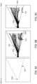
- funnel
- faces
- ion
- electrode tracks
- guard rails
- Prior art date
- Legal status (The legal status is an assumption and is not a legal conclusion. Google has not performed a legal analysis and makes no representation as to the accuracy of the status listed.)
- Active
Links
Images




Classifications
-
- H—ELECTRICITY
- H01—ELECTRIC ELEMENTS
- H01J—ELECTRIC DISCHARGE TUBES OR DISCHARGE LAMPS
- H01J49/00—Particle spectrometers or separator tubes
- H01J49/02—Details
- H01J49/06—Electron- or ion-optical arrangements
- H01J49/062—Ion guides
- H01J49/065—Ion guides having stacked electrodes, e.g. ring stack, plate stack
- H01J49/066—Ion funnels
-
- H—ELECTRICITY
- H01—ELECTRIC ELEMENTS
- H01J—ELECTRIC DISCHARGE TUBES OR DISCHARGE LAMPS
- H01J49/00—Particle spectrometers or separator tubes
- H01J49/02—Details
- H01J49/022—Circuit arrangements, e.g. for generating deviation currents or voltages ; Components associated with high voltage supply
-
- H—ELECTRICITY
- H01—ELECTRIC ELEMENTS
- H01J—ELECTRIC DISCHARGE TUBES OR DISCHARGE LAMPS
- H01J49/00—Particle spectrometers or separator tubes
- H01J49/02—Details
- H01J49/06—Electron- or ion-optical arrangements
-
- H—ELECTRICITY
- H01—ELECTRIC ELEMENTS
- H01J—ELECTRIC DISCHARGE TUBES OR DISCHARGE LAMPS
- H01J49/00—Particle spectrometers or separator tubes
- H01J49/02—Details
- H01J49/06—Electron- or ion-optical arrangements
- H01J49/068—Mounting, supporting, spacing, or insulating electrodes
Definitions
- the present teaching relates to mass spectrometry and in particular to ion funnels that are used in mass spectrometry to direct and focus a beam of ions from an ionization source into a mass spectrometer detector.
- Ion funnels are typically constructed from a stack of plate electrodes (typically 30-100) with decreasing apertures. RF potentials of opposite polarity are applied on adjacent electrodes to create an effective potential- sometimes referred to as a pseudopotential- that radially confines the ions passing through the ion funnel. As successive electrodes have decreasing apertures, the net result is that a spatially dispersed ion cloud entering the ion funnel is efficiently focused to a much smaller radial size on exiting the ion funnel.
- Each of the individual plate electrodes needs to be supplied with individual DC with alternating RF voltages superimposed. The result is there is a complicated kit of parts which need to be assembled with precision in a particular order. Ion funnels can also benefit from a fine pitch of electrodes - something which can be difficult to achieve with conventional ion optics. It will be appreciated that this may require a separate distribution circuit board, typically printed circuit board (PCB), which develops the necessary voltages.
- PCB printed circuit board
- the electrode set either has to be connected via a complex wiring network or integrated to the PCB and soldered directly. The physical size of the sockets or solder pads ultimately limits electrode pitch and this can affect the practical application of these type of devices.
- the fabricated funnel bridges two chambers and its solid construction means that gas cannot escape radially (as is typical of stacked plate ion funnels). This increase the gas load downstream chambers and has the potential for gas flow at the exit to interfere with ion motion in the region of the exit.
- the device is constructed in two halves by soldering a daughter board and then bringing halves together before fixing with adhesive, there is a requirement for a skilled operator- it is very much a manual operation and therefore whilst theoretically advantageous it would appear that it is incompatible at least in part with high volume PCB fabrication techniques.
- the design also suffers in that it introduces a gap in the tracks where the two halves meet which has the potential for ion loss unless gaps are similar to the track spacing further increasing the dependence on precision/tolerancing in construction.
- WO97/49111 describes a method and apparatus for focusing dispersed charged particles. More specifically, a series of elements, each having successively larger apertures forming an ion funnel, wherein RF voltages are applied to the elements so that the RF voltage on any element has phase, amplitude and frequency necessary to define a confinement zone for charged particles of appropriate charge and mass in the interior of the ion funnel, wherein the confinement zone has an acceptance region and an emmitance region and where the acceptance region area is larger than the emmitance region area.
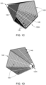
- Figure 1 shows two examples of an ion funnel 100 comprising a plurality of faces 105 in accordance with the present teaching.
- the ion funnel is formed from three faces, whereas in Figure 1C and 1D , the ion funnel is formed from five faces.
- the individual faces are each formed from a printed circuit board and arranged relative to one another such that the ion funnel has a pyramidal structure having a base 110 and an apex 120.
- These exemplary arrangements are fabricated from printed circuit boards, PCBs, that each have a truncated triangular geometrical form. It will be appreciated that this geometry is particularly advantageous in that it facilitates a stacking of the faces edge to edge to form the pyramidal structure defining the ion funnel.
- An entrance 110A to the ion funnel is defined at the base 110 of the ion funnel 100 and an exit 120A from the ion funnel is defined at the apex 120 of the pyramidal structure. It will be appreciated that as the exit 120A is formed from an aperture defined at the apex that the pyramidal structure is effectively a truncated pyramid as the individual triangular faces 105 do not meet physically to form an actual point.
- the funnel is configured to define an ion path within the internal volume of the pyramidal between the entrance 110A and the exit 120A. The ion path extends from the entrance 110A to the exit 120A. A spatially dispersed ion cloud entering the ion funnel at the entrance 110A travelling along the ion path is efficiently focused to a much smaller radial size on exiting the ion funnel's exit 120A.
- This focusing is effected by the provision of a plurality of separate and distinct electrode tracks 130 defined on each of the respective inner surfaces 140 of the plurality of triangular faces.
- the plurality of electrode tracks 130 are arranged substantially transverse to the ion path and extending from the base to the apex.
- adjacent electrode tracks are operatively coupled to both RF and DC voltages to effect RF ion confinement to focus and direct an ion beam towards the exit of the funnel.
- this is effected by the generation of an RF pseudo potential 500 in the region proximate to the individual tracks 130
- the plurality of triangular faces 105 are arranged edge to edge with one another to define the enclosed inner volume 140 within which the ion beam 700 will operatively travel. Whilst they are separate and distinct, the plurality of triangular faces are preferably arranged relative to one another such that each of the electrode tracks on a first triangular face has a corresponding electrode track on a second triangular face.
- the plurality of electrode tracks 130 on each face are desirably separate and distinct from the plurality of electrode tracks on the other faces.
- Each track 130 extends across the inner surface of its respective triangular surface from a first edge region 205 to a second edge region 210. The edge region may not actually be at the side 215 of the face.
- Each of the electrode tracks are optimally substantially parallel with one another and extend substantially transverse to the direction of travel of the ion beam from the entrance to the exit of the funnel.
- the electrode tracks can be fabricated using conventional PCB manufacturing techniques.
- each of the triangular faces preferably has a plurality of slots 150 defined in, and extending through, the substrate defined by the printed circuit board.
- the slots 150 are provided between adjacent tracks 130, and operatively provide an outlet through which a gas may vent through the faces of the funnel.
- By providing the slots 150 cut between the tracks which may be effected using for example in this instance using the standard PCB fabrication techniques. This allows the funnel to vent gas radially which is an advantage over prior art funnels which do not have this capacity with the result that there is an increased gas load on the downstream side of the ion beam. It will be appreciated however that it may be however beneficial in some circumstances to not include these perforations in order to maximise track density by increasing the maximum tolerable space charge.
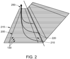
- the funnel further comprises a plurality of guard rails 220 provided at the edges 215 of the triangular faces. Desirably each of the faces have edges that are proximal to, but not fixed to or against, edges of a neighbouring face.
- the guard rails 220 are configured to operatively bias ions 250 away from the edges of the triangular faces, evident from the schematic of Figure 2 .
- the guard rails extending from the base to the apex of the pyramidal structure.
- the guard rails are desirably provided at a higher DC voltage than the electrode tracks. It will be appreciated that ion funnels produced with planar walls tend to concentrate ions up into their corners.
- simulation results demonstrate that having the guard rails on increases the transmission of ions through the funnel from 30% to about 85%, without requiring individual ones of the triangular faces being brought into contact.
- the simulation was effected with the gap between adjacent triangular faces being twice the separation between the electrode tracks on each face. It will be appreciated that this demonstrates that a funnel can be fabricated without the need to bond or otherwise join the individual PCB boards that form the triangular faces. Without the need to solder the boards together they can individually be produced with the normal mass production techniques (e.g. solder re-flow).
- the guard rails are DC biased and may also in certain configurations be also coupled to an RF source.
- the funnel may further comprise bias rails 400 colocated with fixtures such as screw heads provided within the funnel.
- the bias rails 400 are provided at an elevated DC voltage to the electrode tracks and operatively biasing ions away from the fixtures by generating a DC bias potential 420. Ions within the ion flux 700 passing through the funnel are operatively biased away from each of the tracks 50 and the bias rails 400 so as to adopt a path that is generally about a main axis of the pyramidal structure.
- Such an arrangement is particularly advantageous in that it facilitates use of an ion funnel per the present teaching with other external hardware.
- the use of these bias rails with elevated DC can be used to discourage the ions away from fixtures (such as the mentioned screws). This means fixtures can be even be placed within the ion funnel volume. In the absence of these DC bias rails these fixtures would either charge up uncontrollably pinching off ion transmission or - if grounded - extract ions from the funnel reducing signal.
- Figure 8 shows simulated ion trajectories showing a fixture 400 biased even as high as the inlet potential prevents ion loss on an internal fixture. It should be noted that this is a cut though which only shows loses in a narrow band for clarity - ions would be pulled in from all directions.
- the potential should be at a level higher than a potential of local electrodes but there is a significant range of tuning available. This could be fixed by direct connection to another electrical component of fixture. Certain configurations could provide these as tuneable potentials to facilitate changes dependent on location of the fixture and/or the type of mass spectra being analysed.
- Figure 8B shows how a grounded fixture would attract and ultimately discharge ions and therefore presents an alternative exit away from the desired route through the funnel.
- Figure 8C shows ion that a fixture can be incorporated provided it is biased above the ambient DC potential. Some ion trajectories appear to terminate on the 'upstream' side of the fixture but these are in fact diverted round the obstacle in directions outside the viewing plane. In the case of these simulations a potential equal to the funnel's input DC can be used without pinching off ion flow.
- the embodiments disclosed herein reference 3 and 5 sides pyramidal structures. It will be appreciated that per the present teaching three faces, which are typically provided with a truncated triangular geometry, is the minimum number of surfaces required to obtain an enclosed funnel volume necessary for ion enrichment but the present teaching does not need to be considered limited to these 3 and 5 surface configurations. It will be understood that exemplary embodiments of an ion funnel in accordance with the present teaching have been described. The present inventor has identified that it is possible to fabricate an ion guide with at least three sides, each of the sides preferably having a wedge shaped or triangular configuration and being individually planar in form.
- none of the planar sides are parallel with others of the planar sides such that the multiple sides cooperate with one another to adopt a funnel geometry having multiple planar surface which abut one another at respective edges.
Landscapes
- Chemical & Material Sciences (AREA)
- Analytical Chemistry (AREA)
- Electron Tubes For Measurement (AREA)
- Other Investigation Or Analysis Of Materials By Electrical Means (AREA)
Description
- The present teaching relates to mass spectrometry and in particular to ion funnels that are used in mass spectrometry to direct and focus a beam of ions from an ionization source into a mass spectrometer detector.
- Ion funnels are typically constructed from a stack of plate electrodes (typically 30-100) with decreasing apertures. RF potentials of opposite polarity are applied on adjacent electrodes to create an effective potential- sometimes referred to as a pseudopotential- that radially confines the ions passing through the ion funnel. As successive electrodes have decreasing apertures, the net result is that a spatially dispersed ion cloud entering the ion funnel is efficiently focused to a much smaller radial size on exiting the ion funnel.
- Each of the individual plate electrodes needs to be supplied with individual DC with alternating RF voltages superimposed. The result is there is a complicated kit of parts which need to be assembled with precision in a particular order. Ion funnels can also benefit from a fine pitch of electrodes - something which can be difficult to achieve with conventional ion optics. It will be appreciated that this may require a separate distribution circuit board, typically printed circuit board (PCB), which develops the necessary voltages. The electrode set either has to be connected via a complex wiring network or integrated to the PCB and soldered directly. The physical size of the sockets or solder pads ultimately limits electrode pitch and this can affect the practical application of these type of devices.
- Recently there have been developments in the design of ion funnels including the use of printed circuit boards (PCBs). Schlottmann, F., Allers, M., Kirk, A.T. et al. A Simple Printed Circuit Board-Based Ion Funnel for Focusing Low m/z Ratio Ions with High Kinetic Energies at Elevated Pressure. J. Am. Soc. Mass Spectrom. 30, 1813-1823 (2019) discuss the construction of a funnel by bringing together a set of four wedge shaped PCBs to produce a square pyramidal analogue of an ion funnel with the electrodes replaced with tracks. This ultimately defines an asymmetric arrangement which can be complex to assemble whilst ensuring that the functionality of the ion funnel is achieved. Whilst this evidently benefits from use of PCB technology in providing the electrodes the fabricated funnel bridges two chambers and its solid construction means that gas cannot escape radially (as is typical of stacked plate ion funnels). This increase the gas load downstream chambers and has the potential for gas flow at the exit to interfere with ion motion in the region of the exit. Furthermore, as the device is constructed in two halves by soldering a daughter board and then bringing halves together before fixing with adhesive, there is a requirement for a skilled operator- it is very much a manual operation and therefore whilst theoretically advantageous it would appear that it is incompatible at least in part with high volume PCB fabrication techniques. The design also suffers in that it introduces a gap in the tracks where the two halves meet which has the potential for ion loss unless gaps are similar to the track spacing further increasing the dependence on precision/tolerancing in construction.
-
WO97/49111 - Accordingly, there is a need to provide a ion funnel that can address these and other constraints of conventional ion funnels.
- Accordingly there is provided an ion funnel as detailed in
claim 1. Advantageous features are in the dependent claims. - These and other aspects and features will be better understood with reference to the drawings that now follow.
-
-
Figure 1A and Figure 1B show, respectively, perspective views from the base and the apex of a three-sided ion funnel in accordance with the present teaching -
Figure 1C and Figure 1D show, respectively, perspective views from the base and the apex of a five-sided ion funnel in accordance with the present teaching -
Figure 2 shows in schematic form two triangular faces in a non-assembled state outlining the operation of a guard rail in accordance with the present teaching -
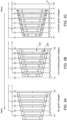
Figure 3A, 3B, and 3C show respectively, schematics of the electronic circuitry that can be used to drive electrical components of triangular faces of a funnel in accordance with the present teaching:Figure 3A shows an arrangement with no guard rails,Figure 3B shows an arrangement with guard rails that are provided out of phase andFigure 3C shows an arrangement with guard rails that are provided in phase -
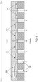
Figure 4 is a side view sectional schematic of portion of a triangular face in accordance with one aspect of the present teaching. -
Figure 5 is a side view sectional schematic of portion of a triangular face in accordance with another aspect of the present teaching. -
Figure 6A and 6B are two electrostatic potential simulation schematics showing the effect of the guard rails being off (6A) and on (6B). -
Figure 7A and 7B are two ion trajectory simulation schematics showing the effect of the guard rails being off (7A) and on (7B). -
Figures 8A, 8B and 8C are schematics showing a cross-section in a plane containing a centreline of an ion funnel in accordance with the present teaching.Figure 8A shows no ions present within the funnel,Figure 8B shows simulated ion trajectories in the presence of a grounded fixture andFigure 8C shows simulated ion trajectories in the presence of a biased fixture inside the funnel. -
Figure 1 shows two examples of anion funnel 100 comprising a plurality offaces 105 in accordance with the present teaching. In the example ofFigure 1A and 1B , the ion funnel is formed from three faces, whereas inFigure 1C and 1D , the ion funnel is formed from five faces. In each example, the individual faces are each formed from a printed circuit board and arranged relative to one another such that the ion funnel has a pyramidal structure having a base 110 and anapex 120. These exemplary arrangements are fabricated from printed circuit boards, PCBs, that each have a truncated triangular geometrical form. It will be appreciated that this geometry is particularly advantageous in that it facilitates a stacking of the faces edge to edge to form the pyramidal structure defining the ion funnel. - An entrance 110A to the ion funnel is defined at the base 110 of the
ion funnel 100 and anexit 120A from the ion funnel is defined at theapex 120 of the pyramidal structure. It will be appreciated that as theexit 120A is formed from an aperture defined at the apex that the pyramidal structure is effectively a truncated pyramid as the individualtriangular faces 105 do not meet physically to form an actual point. The funnel is configured to define an ion path within the internal volume of the pyramidal between the entrance 110A and theexit 120A. The ion path extends from the entrance 110A to theexit 120A. A spatially dispersed ion cloud entering the ion funnel at the entrance 110A travelling along the ion path is efficiently focused to a much smaller radial size on exiting the ion funnel'sexit 120A. - This focusing is effected by the provision of a plurality of separate and
distinct electrode tracks 130 defined on each of the respectiveinner surfaces 140 of the plurality of triangular faces. The plurality ofelectrode tracks 130 are arranged substantially transverse to the ion path and extending from the base to the apex. Similarly to the operation of known ion funnels, adjacent electrode tracks are operatively coupled to both RF and DC voltages to effect RF ion confinement to focus and direct an ion beam towards the exit of the funnel. As is visualised inFigure 5 , this is effected by the generation of anRF pseudo potential 500 in the region proximate to theindividual tracks 130 - As is evident from
Figure 1 but also in the simulation results ofFigure 7 , the plurality oftriangular faces 105 are arranged edge to edge with one another to define the enclosedinner volume 140 within which theion beam 700 will operatively travel. Whilst they are separate and distinct, the plurality of triangular faces are preferably arranged relative to one another such that each of the electrode tracks on a first triangular face has a corresponding electrode track on a second triangular face. - As is visible in each of
Figures 1 ,3 , and7 , the plurality ofelectrode tracks 130 on each face are desirably separate and distinct from the plurality of electrode tracks on the other faces. Eachtrack 130 extends across the inner surface of its respective triangular surface from afirst edge region 205 to asecond edge region 210. The edge region may not actually be at theside 215 of the face. Each of the electrode tracks are optimally substantially parallel with one another and extend substantially transverse to the direction of travel of the ion beam from the entrance to the exit of the funnel. The electrode tracks can be fabricated using conventional PCB manufacturing techniques. - In addition to the electrode tracks, each of the triangular faces preferably has a plurality of slots 150 defined in, and extending through, the substrate defined by the printed circuit board. The slots 150 are provided between
adjacent tracks 130, and operatively provide an outlet through which a gas may vent through the faces of the funnel. By providing the slots 150 cut between the tracks, which may be effected using for example in this instance using the standard PCB fabrication techniques. This allows the funnel to vent gas radially which is an advantage over prior art funnels which do not have this capacity with the result that there is an increased gas load on the downstream side of the ion beam. It will be appreciated however that it may be however beneficial in some circumstances to not include these perforations in order to maximise track density by increasing the maximum tolerable space charge. - As is visible in
Figures 2 and3 the funnel further comprises a plurality ofguard rails 220 provided at theedges 215 of the triangular faces. Desirably each of the faces have edges that are proximal to, but not fixed to or against, edges of a neighbouring face. Theguard rails 220 are configured to operatively biasions 250 away from the edges of the triangular faces, evident from the schematic ofFigure 2 . The guard rails extending from the base to the apex of the pyramidal structure. The guard rails are desirably provided at a higher DC voltage than the electrode tracks. It will be appreciated that ion funnels produced with planar walls tend to concentrate ions up into their corners. This is a natural consequence of the isotropic nature of ion diffusion in the plane perpendicular to device axis and the non-isotropic closing in of the funnel 'walls' as it is traversed. The present inventor has identified that the junctions in PCB ion funnels are therefore critical regions. By placing a set of guard rails or tracks at an elevated DC potential, ions near the edge of the board can be prevented from reaching the corners of the device- the corners being the region between two adjacent triangular faces. This reduces the criticality of the construction of the junctions between PCBs.Figure 7A and Figure 7B show the effect in simulation in having the guard rails off (Figure 7A ) and having the guard rails on (Figure 7B ). simulation results demonstrate that having the guard rails on increases the transmission of ions through the funnel from 30% to about 85%, without requiring individual ones of the triangular faces being brought into contact. In the example ofFigure 7 , the simulation was effected with the gap between adjacent triangular faces being twice the separation between the electrode tracks on each face. It will be appreciated that this demonstrates that a funnel can be fabricated without the need to bond or otherwise join the individual PCB boards that form the triangular faces. Without the need to solder the boards together they can individually be produced with the normal mass production techniques (e.g. solder re-flow). The guard rails are DC biased and may also in certain configurations be also coupled to an RF source. - As is shown in
Figure 4 and8 the funnel may further comprise bias rails 400 colocated with fixtures such as screw heads provided within the funnel. The bias rails 400 are provided at an elevated DC voltage to the electrode tracks and operatively biasing ions away from the fixtures by generating a DC bias potential 420. Ions within theion flux 700 passing through the funnel are operatively biased away from each of the tracks 50 and the bias rails 400 so as to adopt a path that is generally about a main axis of the pyramidal structure. - Such an arrangement is particularly advantageous in that it facilitates use of an ion funnel per the present teaching with other external hardware. The use of these bias rails with elevated DC can be used to discourage the ions away from fixtures (such as the mentioned screws). This means fixtures can be even be placed within the ion funnel volume. In the absence of these DC bias rails these fixtures would either charge up uncontrollably pinching off ion transmission or - if grounded - extract ions from the funnel reducing signal.
Figure 8 shows simulated ion trajectories showing afixture 400 biased even as high as the inlet potential prevents ion loss on an internal fixture. It should be noted that this is a cut though which only shows loses in a narrow band for clarity - ions would be pulled in from all directions. The potential should be at a level higher than a potential of local electrodes but there is a significant range of tuning available. This could be fixed by direct connection to another electrical component of fixture. Certain configurations could provide these as tuneable potentials to facilitate changes dependent on location of the fixture and/or the type of mass spectra being analysed.Figure 8B ) shows how a grounded fixture would attract and ultimately discharge ions and therefore presents an alternative exit away from the desired route through the funnel.Figure 8C ) shows ion that a fixture can be incorporated provided it is biased above the ambient DC potential. Some ion trajectories appear to terminate on the 'upstream' side of the fixture but these are in fact diverted round the obstacle in directions outside the viewing plane. In the case of these simulations a potential equal to the funnel's input DC can be used without pinching off ion flow. - This can be realised by fixing the external end into an insulated insert and supplying DC potential to the head with a specific track for instance via plating through hole from the outside.
- It will be appreciated that the embodiments disclosed herein
reference - Modifications can be made to these exemplary embodiments without departing from the scope of the present teaching which is to be considered limited only insofar as is necessary in the light of the claims that follow.
Claims (13)
- An ion funnel (100) comprising a plurality of individual faces (105), each face being formed from a printed circuit board, the faces being arranged edge to edge relative to one another to form a pyramidal structure having a base (110) and an apex (120), an entrance (110A) to the ion funnel (100) being defined at the base (110) of the pyramidal structure and an exit (120A) from the ion funnel (100) being defined at the apex (120) of the pyramidal structure, the funnel being configured to define an ion path within the pyramidal structure between the entrance and the exit, each of the plurality of faces having a plurality of separate and distinct electrode tracks (130) defined on a respective inner surface (140), the plurality of electrode tracks (130) being arranged substantially transverse to the ion path and extending from the base (110) to the apex (120), and wherein adjacent electrode tracks (130) are operatively coupled to both radio frequency, RF, and DC voltages to effect RF ion confinement to focus and direct an ion beam (700) towards the exit of the funnel, and characterised in that the funnel further comprises DC biased guard rails (220) provided at the edges (215) of each of the faces, the guard rails (220) being configured to operatively bias ions away from the edges of the faces (105), the guard rails (220) extending from the base to the apex of the pyramidal structure
- The funnel of claim 1 wherein the plurality of faces (105) are arranged edge to edge with one another to define an enclosed volume within which the ion beam will operatively travel.
- The funnel of claim 1 or 2 wherein the plurality of faces (105) are arranged relative to one another such that each of the electrode tracks on a first truncated triangular face has a corresponding electrode track (130) on a second truncated triangular face (105).
- The funnel of any preceding claim wherein the plurality of electrode tracks (130) on each face are separate and distinct from the plurality of electrode tracks on the other faces, each track extending across the inner surface of its respective face from a first edge to a second edge.
- The funnel of any preceding claim wherein each of the electrode tracks are parallel with one another.
- The funnel of any preceding claim wherein each of the faces has a plurality of slots (150) defined in, and extending through, the printed circuit board, the slots (150) being provided between adjacent tracks (130), and operatively provide an outlet through which a gas may vent through the faces of the funnel.
- The funnel of any preceding claim wherein the guard rails (220) are provided at a higher DC voltage than the electrode tracks.
- The funnel of any preceding claim further comprising bias rails (400) colocated with fixtures provided within the funnel, the bias rails being provided at an elevated DC voltage to the electrode tracks and operatively biasing ions away from the fixtures.
- The funnel of any preceding claim wherein each of the faces have edges that are proximal to, but not fixed to or against, edges of a neighbouring face.
- The funnel of any preceding claim wherein the guard rails (220) are operatively coupled to an RF source, such that both RF and DC voltages are applied to the guard rails.
- The funnel of any one of claims 1 to 9 wherein the guard rails (220) have DC voltages only applied thereto.
- The funnel of any preceding claim wherein at least a subset of the faces have a truncated triangular geometry.
- The funnel of claim 12 wherein each of the faces (105) have a truncated triangular geometry.
Applications Claiming Priority (2)
| Application Number | Priority Date | Filing Date | Title |
|---|---|---|---|
| GB2008720.1A GB2595876B (en) | 2020-06-09 | 2020-06-09 | Mass spectrometry ion funnel |
| PCT/EP2021/064356 WO2021249790A1 (en) | 2020-06-09 | 2021-05-28 | Mass spectrometry ion funnel |
Publications (3)
| Publication Number | Publication Date |
|---|---|
| EP4121999A1 EP4121999A1 (en) | 2023-01-25 |
| EP4121999C0 EP4121999C0 (en) | 2024-12-11 |
| EP4121999B1 true EP4121999B1 (en) | 2024-12-11 |
Family
ID=71615977
Family Applications (1)
| Application Number | Title | Priority Date | Filing Date |
|---|---|---|---|
| EP21735163.4A Active EP4121999B1 (en) | 2020-06-09 | 2021-05-28 | Mass spectrometry ion funnel |
Country Status (6)
| Country | Link |
|---|---|
| US (1) | US11631576B1 (en) |
| EP (1) | EP4121999B1 (en) |
| JP (1) | JP7344407B2 (en) |
| CN (1) | CN115699249A (en) |
| GB (1) | GB2595876B (en) |
| WO (1) | WO2021249790A1 (en) |
Families Citing this family (1)
| Publication number | Priority date | Publication date | Assignee | Title |
|---|---|---|---|---|
| CN119480609B (en) * | 2024-11-18 | 2025-10-31 | 中国科学院大连化学物理研究所 | A tripolar ion funnel device for efficient ion transport over a wide mass range |
Family Cites Families (20)
| Publication number | Priority date | Publication date | Assignee | Title |
|---|---|---|---|---|
| WO1997049111A1 (en) * | 1996-06-17 | 1997-12-24 | Battelle Memorial Institute | Method and apparatus for ion and charged particle focusing |
| US7064321B2 (en) | 2003-04-08 | 2006-06-20 | Bruker Daltonik Gmbh | Ion funnel with improved ion screening |
| US7569811B2 (en) | 2006-01-13 | 2009-08-04 | Ionics Mass Spectrometry Group Inc. | Concentrating mass spectrometer ion guide, spectrometer and method |
| US10991545B2 (en) * | 2008-06-30 | 2021-04-27 | Nexgen Semi Holding, Inc. | Method and device for spatial charged particle bunching |
| US7838826B1 (en) * | 2008-08-07 | 2010-11-23 | Bruker Daltonics, Inc. | Apparatus and method for parallel flow ion mobility spectrometry combined with mass spectrometry |
| US7851745B2 (en) | 2008-12-12 | 2010-12-14 | Thermo Finnigan Llc | Flat plate FAIMS with lateral ion focusing |
| US8324565B2 (en) * | 2009-12-17 | 2012-12-04 | Agilent Technologies, Inc. | Ion funnel for mass spectrometry |
| EP2405463A1 (en) | 2010-07-06 | 2012-01-11 | ETH Zurich | Laser-ablation ion source with ion funnel |
| US9230790B2 (en) * | 2011-12-30 | 2016-01-05 | Dh Technologies Development Pte. Ltd. | DC ion funnels |
| US9053915B2 (en) | 2012-09-25 | 2015-06-09 | Agilent Technologies, Inc. | Radio frequency (RF) ion guide for improved performance in mass spectrometers at high pressure |
| US8779353B2 (en) | 2012-01-11 | 2014-07-15 | Bruker Daltonics, Inc. | Ion guide and electrode for its assembly |
| US9147567B2 (en) | 2012-02-01 | 2015-09-29 | Dh Technologies Development Pte. Ltd. | Method and apparatus for improved sensitivity in a mass spectrometer |
| JP6027239B2 (en) * | 2012-07-31 | 2016-11-16 | レコ コーポレイションLeco Corporation | Ion mobility spectrometer with high throughput |
| US9824874B2 (en) * | 2014-06-10 | 2017-11-21 | Battelle Memorial Institute | Ion funnel device |
| CN105470094B (en) | 2014-09-04 | 2018-03-09 | 株式会社岛津制作所 | Ion optics and mass spectrograph |
| US10211040B2 (en) * | 2014-11-07 | 2019-02-19 | The Trustees Of Indiana University | Frequency and amplitude scanned quadrupole mass filter and methods |
| US9449804B2 (en) | 2014-11-11 | 2016-09-20 | Agilent Technologies, Inc. | Dual field multipole converging ion guides, hyperbolic ion guides, and related methods |
| US10332723B1 (en) * | 2017-12-20 | 2019-06-25 | Battelle Memorial Institute | Ion focusing device |
| CN209675238U (en) * | 2019-05-23 | 2019-11-22 | 北京理工大学 | A kind of ion funnel device and Mass Spectrometer Method system |
| CN111081528A (en) * | 2019-12-20 | 2020-04-28 | 暨南大学 | Funnel-shaped ion guide device and mass spectrometer with same |
-
2020
- 2020-06-09 GB GB2008720.1A patent/GB2595876B/en active Active
-
2021
- 2021-05-28 JP JP2022575176A patent/JP7344407B2/en active Active
- 2021-05-28 EP EP21735163.4A patent/EP4121999B1/en active Active
- 2021-05-28 WO PCT/EP2021/064356 patent/WO2021249790A1/en not_active Ceased
- 2021-05-28 CN CN202180037072.1A patent/CN115699249A/en active Pending
- 2021-05-28 US US17/925,374 patent/US11631576B1/en active Active
Also Published As
| Publication number | Publication date |
|---|---|
| JP2023520261A (en) | 2023-05-16 |
| GB2595876A (en) | 2021-12-15 |
| EP4121999A1 (en) | 2023-01-25 |
| US11631576B1 (en) | 2023-04-18 |
| JP7344407B2 (en) | 2023-09-13 |
| GB2595876B (en) | 2024-02-07 |
| EP4121999C0 (en) | 2024-12-11 |
| WO2021249790A9 (en) | 2022-03-17 |
| WO2021249790A1 (en) | 2021-12-16 |
| GB202008720D0 (en) | 2020-07-22 |
| CN115699249A (en) | 2023-02-03 |
Similar Documents
| Publication | Publication Date | Title |
|---|---|---|
| US12125694B2 (en) | Ion mirror for multi-reflecting mass spectrometers | |
| JP4463271B2 (en) | Asymmetric field ion guide device | |
| US7498569B2 (en) | Ion trap mass analyzer | |
| CN105470094B (en) | Ion optics and mass spectrograph | |
| CN104641451B (en) | Improved ion guide | |
| US9867272B2 (en) | Generation and acceleration of charged particles using compact devices and systems | |
| JP6443465B2 (en) | Ion manipulation device for guiding or confining ions in an ion processing device | |
| US20200185209A1 (en) | Electrode array devices and methods | |
| US11631576B1 (en) | Mass spectrometry ion funnel | |
| US9524857B2 (en) | Ion optics components and method of making the same | |
| CN110504152A (en) | Ion guide | |
| Ji et al. | Beam power scale-up in micro-electromechanical systems based multi-beam ion accelerators | |
| Persaud et al. | A compact linear accelerator based on a scalable microelectromechanical-system RF-structure | |
| JP4766170B2 (en) | Mass spectrometer | |
| JP7322650B2 (en) | Multi-turn time-of-flight mass spectrometer and manufacturing method thereof | |
| US6326746B1 (en) | High efficiency resonator for linear accelerator | |
| Gasik et al. | Building a large-area GEM-based readout chamber for the upgrade of the ALICE TPC | |
| US7067980B2 (en) | Shinged structures for vacuum microelectronics and methods of manufacturing same | |
| US9386681B2 (en) | Particle accelerator and method of reducing beam divergence in the particle accelerator | |
| EP4020523B1 (en) | Manufacturing method for an ion guide | |
| RU2163426C1 (en) | Multichannel accelerating structure for linear resonance ion accelerator | |
| CN113316834A (en) | Electrode assembly for mass spectrometer | |
| Guharay et al. | Efficient low‐energy beam transport for intense, high‐brightness H− beams in high energy accelerators: Perspectives and a solution using ESQ lensesa | |
| Hoffrogge | A surface-electrode quadrupole guide for electrons | |
| CN120693677A (en) | Ion beam focusing |
Legal Events
| Date | Code | Title | Description |
|---|---|---|---|
| STAA | Information on the status of an ep patent application or granted ep patent |
Free format text: STATUS: UNKNOWN |
|
| STAA | Information on the status of an ep patent application or granted ep patent |
Free format text: STATUS: THE INTERNATIONAL PUBLICATION HAS BEEN MADE |
|
| PUAI | Public reference made under article 153(3) epc to a published international application that has entered the european phase |
Free format text: ORIGINAL CODE: 0009012 |
|
| STAA | Information on the status of an ep patent application or granted ep patent |
Free format text: STATUS: REQUEST FOR EXAMINATION WAS MADE |
|
| 17P | Request for examination filed |
Effective date: 20221021 |
|
| AK | Designated contracting states |
Kind code of ref document: A1 Designated state(s): AL AT BE BG CH CY CZ DE DK EE ES FI FR GB GR HR HU IE IS IT LI LT LU LV MC MK MT NL NO PL PT RO RS SE SI SK SM TR |
|
| DAV | Request for validation of the european patent (deleted) | ||
| DAX | Request for extension of the european patent (deleted) | ||
| GRAP | Despatch of communication of intention to grant a patent |
Free format text: ORIGINAL CODE: EPIDOSNIGR1 |
|
| STAA | Information on the status of an ep patent application or granted ep patent |
Free format text: STATUS: GRANT OF PATENT IS INTENDED |
|
| INTG | Intention to grant announced |
Effective date: 20240529 |
|
| RAP3 | Party data changed (applicant data changed or rights of an application transferred) |
Owner name: MICROSAIC SYSTEMS PLC |
|
| GRAS | Grant fee paid |
Free format text: ORIGINAL CODE: EPIDOSNIGR3 |
|
| GRAA | (expected) grant |
Free format text: ORIGINAL CODE: 0009210 |
|
| STAA | Information on the status of an ep patent application or granted ep patent |
Free format text: STATUS: THE PATENT HAS BEEN GRANTED |
|
| AK | Designated contracting states |
Kind code of ref document: B1 Designated state(s): AL AT BE BG CH CY CZ DE DK EE ES FI FR GB GR HR HU IE IS IT LI LT LU LV MC MK MT NL NO PL PT RO RS SE SI SK SM TR |
|
| REG | Reference to a national code |
Ref country code: GB Ref legal event code: FG4D |
|
| REG | Reference to a national code |
Ref country code: CH Ref legal event code: EP |
|
| REG | Reference to a national code |
Ref country code: IE Ref legal event code: FG4D |
|
| REG | Reference to a national code |
Ref country code: DE Ref legal event code: R096 Ref document number: 602021023278 Country of ref document: DE |
|
| U01 | Request for unitary effect filed |
Effective date: 20241211 |
|
| U07 | Unitary effect registered |
Designated state(s): AT BE BG DE DK EE FI FR IT LT LU LV MT NL PT RO SE SI Effective date: 20241218 |
|
| PG25 | Lapsed in a contracting state [announced via postgrant information from national office to epo] |
Ref country code: HR Free format text: LAPSE BECAUSE OF FAILURE TO SUBMIT A TRANSLATION OF THE DESCRIPTION OR TO PAY THE FEE WITHIN THE PRESCRIBED TIME-LIMIT Effective date: 20241211 |
|
| PG25 | Lapsed in a contracting state [announced via postgrant information from national office to epo] |
Ref country code: ES Free format text: LAPSE BECAUSE OF FAILURE TO SUBMIT A TRANSLATION OF THE DESCRIPTION OR TO PAY THE FEE WITHIN THE PRESCRIBED TIME-LIMIT Effective date: 20241211 |
|
| PG25 | Lapsed in a contracting state [announced via postgrant information from national office to epo] |
Ref country code: NO Free format text: LAPSE BECAUSE OF FAILURE TO SUBMIT A TRANSLATION OF THE DESCRIPTION OR TO PAY THE FEE WITHIN THE PRESCRIBED TIME-LIMIT Effective date: 20250311 |
|
| PG25 | Lapsed in a contracting state [announced via postgrant information from national office to epo] |
Ref country code: GR Free format text: LAPSE BECAUSE OF FAILURE TO SUBMIT A TRANSLATION OF THE DESCRIPTION OR TO PAY THE FEE WITHIN THE PRESCRIBED TIME-LIMIT Effective date: 20250312 |
|
| PG25 | Lapsed in a contracting state [announced via postgrant information from national office to epo] |
Ref country code: RS Free format text: LAPSE BECAUSE OF FAILURE TO SUBMIT A TRANSLATION OF THE DESCRIPTION OR TO PAY THE FEE WITHIN THE PRESCRIBED TIME-LIMIT Effective date: 20250311 |
|
| PG25 | Lapsed in a contracting state [announced via postgrant information from national office to epo] |
Ref country code: SM Free format text: LAPSE BECAUSE OF FAILURE TO SUBMIT A TRANSLATION OF THE DESCRIPTION OR TO PAY THE FEE WITHIN THE PRESCRIBED TIME-LIMIT Effective date: 20241211 |
|
| PG25 | Lapsed in a contracting state [announced via postgrant information from national office to epo] |
Ref country code: PL Free format text: LAPSE BECAUSE OF FAILURE TO SUBMIT A TRANSLATION OF THE DESCRIPTION OR TO PAY THE FEE WITHIN THE PRESCRIBED TIME-LIMIT Effective date: 20241211 |
|
| PG25 | Lapsed in a contracting state [announced via postgrant information from national office to epo] |
Ref country code: IS Free format text: LAPSE BECAUSE OF FAILURE TO SUBMIT A TRANSLATION OF THE DESCRIPTION OR TO PAY THE FEE WITHIN THE PRESCRIBED TIME-LIMIT Effective date: 20250411 |
|
| PG25 | Lapsed in a contracting state [announced via postgrant information from national office to epo] |
Ref country code: SK Free format text: LAPSE BECAUSE OF FAILURE TO SUBMIT A TRANSLATION OF THE DESCRIPTION OR TO PAY THE FEE WITHIN THE PRESCRIBED TIME-LIMIT Effective date: 20241211 |
|
| PG25 | Lapsed in a contracting state [announced via postgrant information from national office to epo] |
Ref country code: CZ Free format text: LAPSE BECAUSE OF FAILURE TO SUBMIT A TRANSLATION OF THE DESCRIPTION OR TO PAY THE FEE WITHIN THE PRESCRIBED TIME-LIMIT Effective date: 20241211 |
|
| PLBE | No opposition filed within time limit |
Free format text: ORIGINAL CODE: 0009261 |
|
| STAA | Information on the status of an ep patent application or granted ep patent |
Free format text: STATUS: NO OPPOSITION FILED WITHIN TIME LIMIT |
|
| REG | Reference to a national code |
Ref country code: CH Ref legal event code: L10 Free format text: ST27 STATUS EVENT CODE: U-0-0-L10-L00 (AS PROVIDED BY THE NATIONAL OFFICE) Effective date: 20251022 |
|
| 26N | No opposition filed |
Effective date: 20250912 |
|
| REG | Reference to a national code |
Ref country code: CH Ref legal event code: H13 Free format text: ST27 STATUS EVENT CODE: U-0-0-H10-H13 (AS PROVIDED BY THE NATIONAL OFFICE) Effective date: 20251223 |
|
| U21 | Renewal fee for the european patent with unitary effect paid with additional fee |
Year of fee payment: 5 Effective date: 20251119 |
|
| PG25 | Lapsed in a contracting state [announced via postgrant information from national office to epo] |
Ref country code: CH Free format text: LAPSE BECAUSE OF NON-PAYMENT OF DUE FEES Effective date: 20250531 |
|
| GBPC | Gb: european patent ceased through non-payment of renewal fee |
Effective date: 20250528 |
|
| PG25 | Lapsed in a contracting state [announced via postgrant information from national office to epo] |
Ref country code: MC Free format text: LAPSE BECAUSE OF FAILURE TO SUBMIT A TRANSLATION OF THE DESCRIPTION OR TO PAY THE FEE WITHIN THE PRESCRIBED TIME-LIMIT Effective date: 20241211 |
|
| PG25 | Lapsed in a contracting state [announced via postgrant information from national office to epo] |
Ref country code: GB Free format text: LAPSE BECAUSE OF NON-PAYMENT OF DUE FEES Effective date: 20250528 |
|
| PG25 | Lapsed in a contracting state [announced via postgrant information from national office to epo] |
Ref country code: IE Free format text: LAPSE BECAUSE OF NON-PAYMENT OF DUE FEES Effective date: 20250528 |