EP4120371A1 - Light source module - Google Patents
Light source module Download PDFInfo
- Publication number
- EP4120371A1 EP4120371A1 EP21767915.8A EP21767915A EP4120371A1 EP 4120371 A1 EP4120371 A1 EP 4120371A1 EP 21767915 A EP21767915 A EP 21767915A EP 4120371 A1 EP4120371 A1 EP 4120371A1
- Authority
- EP
- European Patent Office
- Prior art keywords
- guide layer
- light guide
- light
- light source
- thickness
- Prior art date
- Legal status (The legal status is an assumption and is not a legal conclusion. Google has not performed a legal analysis and makes no representation as to the accuracy of the status listed.)
- Pending
Links
Images



Classifications
-
- G—PHYSICS
- G02—OPTICS
- G02B—OPTICAL ELEMENTS, SYSTEMS OR APPARATUS
- G02B6/00—Light guides; Structural details of arrangements comprising light guides and other optical elements, e.g. couplings
- G02B6/0001—Light guides; Structural details of arrangements comprising light guides and other optical elements, e.g. couplings specially adapted for lighting devices or systems
- G02B6/0011—Light guides; Structural details of arrangements comprising light guides and other optical elements, e.g. couplings specially adapted for lighting devices or systems the light guides being planar or of plate-like form
- G02B6/0065—Manufacturing aspects; Material aspects
-
- H—ELECTRICITY
- H10—SEMICONDUCTOR DEVICES; ELECTRIC SOLID-STATE DEVICES NOT OTHERWISE PROVIDED FOR
- H10H—INORGANIC LIGHT-EMITTING SEMICONDUCTOR DEVICES HAVING POTENTIAL BARRIERS
- H10H20/00—Individual inorganic light-emitting semiconductor devices having potential barriers, e.g. light-emitting diodes [LED]
- H10H20/80—Constructional details
- H10H20/85—Packages
- H10H20/855—Optical field-shaping means, e.g. lenses
-
- G—PHYSICS
- G02—OPTICS
- G02B—OPTICAL ELEMENTS, SYSTEMS OR APPARATUS
- G02B6/00—Light guides; Structural details of arrangements comprising light guides and other optical elements, e.g. couplings
- G02B6/0001—Light guides; Structural details of arrangements comprising light guides and other optical elements, e.g. couplings specially adapted for lighting devices or systems
- G02B6/0011—Light guides; Structural details of arrangements comprising light guides and other optical elements, e.g. couplings specially adapted for lighting devices or systems the light guides being planar or of plate-like form
- G02B6/0013—Means for improving the coupling-in of light from the light source into the light guide
- G02B6/0015—Means for improving the coupling-in of light from the light source into the light guide provided on the surface of the light guide or in the bulk of it
- G02B6/002—Means for improving the coupling-in of light from the light source into the light guide provided on the surface of the light guide or in the bulk of it by shaping at least a portion of the light guide, e.g. with collimating, focussing or diverging surfaces
- G02B6/0021—Means for improving the coupling-in of light from the light source into the light guide provided on the surface of the light guide or in the bulk of it by shaping at least a portion of the light guide, e.g. with collimating, focussing or diverging surfaces for housing at least a part of the light source, e.g. by forming holes or recesses
-
- G—PHYSICS
- G02—OPTICS
- G02B—OPTICAL ELEMENTS, SYSTEMS OR APPARATUS
- G02B5/00—Optical elements other than lenses
- G02B5/08—Mirrors
-
- G—PHYSICS
- G02—OPTICS
- G02B—OPTICAL ELEMENTS, SYSTEMS OR APPARATUS
- G02B5/00—Optical elements other than lenses
- G02B5/08—Mirrors
- G02B5/0808—Mirrors having a single reflecting layer
-
- G—PHYSICS
- G02—OPTICS
- G02B—OPTICAL ELEMENTS, SYSTEMS OR APPARATUS
- G02B6/00—Light guides; Structural details of arrangements comprising light guides and other optical elements, e.g. couplings
- G02B6/0001—Light guides; Structural details of arrangements comprising light guides and other optical elements, e.g. couplings specially adapted for lighting devices or systems
- G02B6/0011—Light guides; Structural details of arrangements comprising light guides and other optical elements, e.g. couplings specially adapted for lighting devices or systems the light guides being planar or of plate-like form
- G02B6/0066—Light guides; Structural details of arrangements comprising light guides and other optical elements, e.g. couplings specially adapted for lighting devices or systems the light guides being planar or of plate-like form characterised by the light source being coupled to the light guide
- G02B6/0068—Arrangements of plural sources, e.g. multi-colour light sources
-
- G—PHYSICS
- G02—OPTICS
- G02B—OPTICAL ELEMENTS, SYSTEMS OR APPARATUS
- G02B6/00—Light guides; Structural details of arrangements comprising light guides and other optical elements, e.g. couplings
- G02B6/0001—Light guides; Structural details of arrangements comprising light guides and other optical elements, e.g. couplings specially adapted for lighting devices or systems
- G02B6/0011—Light guides; Structural details of arrangements comprising light guides and other optical elements, e.g. couplings specially adapted for lighting devices or systems the light guides being planar or of plate-like form
- G02B6/0066—Light guides; Structural details of arrangements comprising light guides and other optical elements, e.g. couplings specially adapted for lighting devices or systems the light guides being planar or of plate-like form characterised by the light source being coupled to the light guide
- G02B6/0073—Light emitting diode [LED]
-
- G—PHYSICS
- G02—OPTICS
- G02B—OPTICAL ELEMENTS, SYSTEMS OR APPARATUS
- G02B6/00—Light guides; Structural details of arrangements comprising light guides and other optical elements, e.g. couplings
- G02B6/10—Light guides; Structural details of arrangements comprising light guides and other optical elements, e.g. couplings of the optical waveguide type
-
- H—ELECTRICITY
- H10—SEMICONDUCTOR DEVICES; ELECTRIC SOLID-STATE DEVICES NOT OTHERWISE PROVIDED FOR
- H10H—INORGANIC LIGHT-EMITTING SEMICONDUCTOR DEVICES HAVING POTENTIAL BARRIERS
- H10H20/00—Individual inorganic light-emitting semiconductor devices having potential barriers, e.g. light-emitting diodes [LED]
- H10H20/80—Constructional details
- H10H20/85—Packages
- H10H20/852—Encapsulations
- H10H20/853—Encapsulations characterised by their shape
-
- H—ELECTRICITY
- H10—SEMICONDUCTOR DEVICES; ELECTRIC SOLID-STATE DEVICES NOT OTHERWISE PROVIDED FOR
- H10H—INORGANIC LIGHT-EMITTING SEMICONDUCTOR DEVICES HAVING POTENTIAL BARRIERS
- H10H29/00—Integrated devices, or assemblies of multiple devices, comprising at least one light-emitting semiconductor element covered by group H10H20/00
- H10H29/10—Integrated devices comprising at least one light-emitting semiconductor component covered by group H10H20/00
- H10H29/14—Integrated devices comprising at least one light-emitting semiconductor component covered by group H10H20/00 comprising multiple light-emitting semiconductor components
- H10H29/142—Two-dimensional arrangements, e.g. asymmetric LED layout
-
- G—PHYSICS
- G02—OPTICS
- G02B—OPTICAL ELEMENTS, SYSTEMS OR APPARATUS
- G02B6/00—Light guides; Structural details of arrangements comprising light guides and other optical elements, e.g. couplings
- G02B6/0001—Light guides; Structural details of arrangements comprising light guides and other optical elements, e.g. couplings specially adapted for lighting devices or systems
- G02B6/0011—Light guides; Structural details of arrangements comprising light guides and other optical elements, e.g. couplings specially adapted for lighting devices or systems the light guides being planar or of plate-like form
- G02B6/0033—Means for improving the coupling-out of light from the light guide
- G02B6/005—Means for improving the coupling-out of light from the light guide provided by one optical element, or plurality thereof, placed on the light output side of the light guide
- G02B6/0055—Reflecting element, sheet or layer
-
- H—ELECTRICITY
- H10—SEMICONDUCTOR DEVICES; ELECTRIC SOLID-STATE DEVICES NOT OTHERWISE PROVIDED FOR
- H10H—INORGANIC LIGHT-EMITTING SEMICONDUCTOR DEVICES HAVING POTENTIAL BARRIERS
- H10H20/00—Individual inorganic light-emitting semiconductor devices having potential barriers, e.g. light-emitting diodes [LED]
- H10H20/80—Constructional details
- H10H20/85—Packages
- H10H20/852—Encapsulations
- H10H20/854—Encapsulations characterised by their material, e.g. epoxy or silicone resins
-
- H—ELECTRICITY
- H10—SEMICONDUCTOR DEVICES; ELECTRIC SOLID-STATE DEVICES NOT OTHERWISE PROVIDED FOR
- H10H—INORGANIC LIGHT-EMITTING SEMICONDUCTOR DEVICES HAVING POTENTIAL BARRIERS
- H10H20/00—Individual inorganic light-emitting semiconductor devices having potential barriers, e.g. light-emitting diodes [LED]
- H10H20/80—Constructional details
- H10H20/85—Packages
- H10H20/855—Optical field-shaping means, e.g. lenses
- H10H20/856—Reflecting means
Definitions
- the present invention since light is irradiated to a first light guide layer and a second light guide layer having different refractive indices, there is an advantage in that the light uniformity is increased and hot spots can be removed.
- FIG. 1 is a cross-sectional view of a light source module according to an embodiment of the present invention
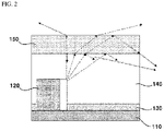
- FIG. 2 is an enlarged view in which a part of FIG. 1 is enlarged
- FIG. 3 is a view comparing the irradiation angle of light according to the difference in materials of the first light guide layer and the second light guide layer
- FIG. 4 is a view comparing hot spots according to the difference in materials of the first light guide layer and the second light guide layer
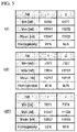
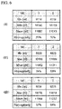
- FIGS. 5 to 7 are charts comparing the light uniformity according to the thickness of the first light guide layer and the second light guide layer.
Landscapes
- Physics & Mathematics (AREA)
- General Physics & Mathematics (AREA)
- Optics & Photonics (AREA)
- Engineering & Computer Science (AREA)
- Manufacturing & Machinery (AREA)
- Microelectronics & Electronic Packaging (AREA)
- Planar Illumination Modules (AREA)
Abstract
Description
- The present embodiment relates to a light source module.
- The content described below provides background information on the present embodiment and does not describe the prior art.
- A light source module using various light sources used in electronic devices is implemented in a way to increase light efficiency by utilizing a suitable light source according to the characteristics of each electronic device.
- Recently, the light source module used in such electronic devices can be variously applied to backlight units being applied to flat panel displays, or indoor lamps being used in an indoor environment, or headlamps, fog lamps, reversing lamps, side lamps, number lamps, tail lamps, brake lamps, direction indicator lamps, emergency flashing lights being installed outside the automobiles, and indoor lightings being installed inside the automobiles.
- Meanwhile, efforts to improve the luminous efficiency of LEDs are continuously progressing from chips to packages. For example, in a packaging stage, a relatively high current is applied using a material having good heat dissipation efficiency using a heat sink to form a thermally stable structure, and efforts are being made to increase light extraction efficiency with an optimal design considering the optical structure and characteristics of the package.
- However, although significant parts of such efforts have been achieving certain degrees of effects at the laboratory level, there are considerable difficulties in applying them to actual manufacturing processes.
- The present embodiment is intended to provide a light source module having a high light efficiency by improving the structure and capable of removing a hot spot for a surface light source.
- In addition, it is intended to provide a light source module in which a separate layer is implemented to remove the hot spots of the LED, the process is simplified by simplifying the structure in a structure where multiple processes are applied, and at the same time, a uniform surface light source is provided.
- As an embodiment, a light source module comprises: a printed circuit board; a light source being disposed on the printed circuit board; a first light guide layer being disposed on the printed circuit board, and accommodating the light source; and a second light guide layer being disposed at an upper portion of the first light guide layer, wherein the material of the first light guide layer is different from the material of the second light guide layer, and wherein the refractive index of the first light guide layer is greater than the refractive index of the second light guide layer. The material of the first light guide layer may include silicon, and the material of the second light guide layer may include barium sulfate and resin.
- The composition ratio of the barium sulfate to the resin may be 1:4.
- The thickness of the first light guide layer may be greater than the thickness of the second light guide layer.
- The light source may be a side view type light emitting diode.
- It may include a light reflective layer being disposed on the printed circuit board and reflecting the light irradiated from the light source.
- The refractive index of the first light guide layer may be 1.5 to 1.6 or less, and the refractive index of the second light guide layer may be 1.4 to 1.5 or less.
- The thickness of the first light guide layer may be 2 mm to 4 mm or less, and the thickness of the second light guide layer may be 0.4 mm to 1.0 mm or less.
- Based on the thickness of the first light guide layer, the thickness of the second light guide layer may be 0.13 to 0.34 or less.
- As another embodiment, a light source module comprises: a printed circuit board; a light source being disposed on the printed circuit board; a first light guide layer being disposed on the printed circuit board and accommodating the light source; and a second light guide layer being disposed at an upper portion of the first light guide layer,
wherein the material of the first light guide layer is different from the material of the second light guide layer, and wherein the thickness of the first light guide layer is greater than the thickness of the second light guide layer. - According to the present invention, since light is irradiated to a first light guide layer and a second light guide layer having different refractive indices, there is an advantage in that the light uniformity is increased and hot spots can be removed.
-
-
FIG. 1 is a cross-sectional view of a light source module according to an embodiment of the present invention. -
FIG. 2 is an enlarged view in which a part ofFIG. 1 is enlarged. -
FIG. 3 is a view comparing the irradiation angle of light according to the difference in materials of the first light guide layer and the second light guide layer. -
FIG. 4 is a view comparing hot spots according to the difference in materials of the first light guide layer and the second light guide layer. -
FIGS. 5 to 7 are charts comparing the light uniformity according to the thickness of the first light guide layer and the second light guide layer. - Hereinafter, preferred embodiments of the present invention will be described in detail with reference to the accompanying drawings.
- However, the technical idea of the present invention is not limited to some embodiments to be described, but may be implemented in various forms, and within the scope of the technical idea of the present invention, one or more of the constituent elements may be selectively combined or substituted between embodiments.
- In addition, the terms (including technical and scientific terms) used in the embodiments of the present invention, unless explicitly defined and described, can be interpreted as a meaning that can be generally understood by a person skilled in the art, and commonly used terms such as terms defined in the dictionary may be interpreted in consideration of the meaning of the context of the related technology.
- In addition, terms used in the present specification are for describing embodiments and are not intended to limit the present invention. In the present specification, the singular form may include the plural form unless specifically stated in the phrase, and when described as "at least one (or more than one) of A and B and C", it may include one or more of all combinations that can be combined with A, B, and C.
- In addition, in describing the components of the embodiment of the present invention, terms such as first, second, A, B, (a), and (b) may be used.
- These terms are merely intended to distinguish the components from other components, and the terms do not limit the nature, order or sequence of the components.
- And, when a component is described as being 'connected', 'coupled' or 'interconnected' to another component, the component is not only directly connected, coupled or interconnected to the other component, but may also include cases of being 'connected', 'coupled', or 'interconnected' due that another component between that other components.
- In addition, when described as being formed or arranged in "on (above)" or "below (under)" of each component, "on (above)" or "below (under)" means that it includes not only the case where the two components are directly in contact with, but also the case where one or more other components are formed or arranged between the two components. In addition, when expressed as "on (above)" or "below (under)", the meaning of not only an upward direction but also a downward direction based on one component may be included.
-
FIG. 1 is a cross-sectional view of a light source module according to an embodiment of the present invention;FIG. 2 is an enlarged view in which a part ofFIG. 1 is enlarged;FIG. 3 is a view comparing the irradiation angle of light according to the difference in materials of the first light guide layer and the second light guide layer;FIG. 4 is a view comparing hot spots according to the difference in materials of the first light guide layer and the second light guide layer; andFIGS. 5 to 7 are charts comparing the light uniformity according to the thickness of the first light guide layer and the second light guide layer. - Referring to
FIGS. 1 and2 , thelight source module 100 according to an embodiment of the present invention may comprise a printedcircuit board 110, alight source 120, alight reflection layer 130, a firstlight guide layer 140, and a secondlight guide layer 150. - The printed
circuit board 110 may be formed in a plate shape, and thelight source 120 may be mounted on an upper surface. Thelight source 120 may include a light emitting diode (LED). Thelight source 120 may be provided in plurality, and may be disposed on the printedcircuit board 110 to be spaced apart from each other. Thelight source 120 may provide light. Thelight source 120 may be a side view type light emitting diode. Unlike this, thelight source 120 may be a downward direction type light emitting diode. - The
light reflection layer 130 may be disposed on an upper surface of the printedcircuit board 110. Thelight reflection layer 130 may be formed in a plate shape and disposed on the printedcircuit board 110. Thelight reflection layer 130 may reflect the light generated from thelight source 120 to the area to be irradiated. A hole forming an arrangement area of thelight source 120 may be formed in thelight reflection layer 130. Thelight source 120 may be mounted on the printedcircuit board 110 through the hole. A plurality of reflective patterns (not shown) may be disposed on the lightreflective layer 130. A plurality of reflective patterns (not shown) may further reflect the light generated from thelight source 120 to an upper region, and the area of each of the reflective patterns increases as the distance from thelight source 120 increases, or, the plurality of reflective patterns may be disposed to include a region in which the density increases. Since the emitted light from thelight source 120 becomes weaker as it moves away from thelight source 120, in order to realize the uniformity of the light of thelight source module 100, the more the emitted light must be reflected upward from thelight source 120 as it moves away from thelight source 120 and therefore the arrangement of the plurality of reflective patterns (not shown) may proceed as described above. - A first
light guide layer 140 and a secondlight guide layer 150 may be disposed on the printedcircuit board 110 and thelight reflection layer 130. The firstlight guide layer 140 and the secondlight guide layer 150 may be stacked in an up and down direction. The light source may be accommodated in the firstlight guide layer 140. - The first
light guide layer 140 may be formed to have a first thickness T1. The secondlight guide layer 150 may be formed to have a second thickness T2. The first thickness T1 may be greater than the second thickness T2. The upper surface of the firstlight guide layer 140 may be disposed higher than the upper surface of thelight source 120. The first thickness T1 may be formed to be greater than the height of thelight source 120. - Materials of the first
light guide layer 140 and the secondlight guide layer 150 may be different from each other. For example, the material of the firstlight guide layer 140 may be silicon. The secondlight guide layer 150 may be made of a material being mixed with barium sulfate and resin. The secondlight guide layer 150 may be made of a material in which barium sulfate and resin are mixed in a ratio of 1:4. Accordingly, the firstlight guide layer 140 and the secondlight guide layer 150 may have different refractive indices. The refractive index of the firstlight guide layer 140 may be greater than that of the secondlight guide layer 150. - For example, the refractive index of the first
light guide layer 140 may form a range of 1.5 to 1.6. The refractive index of the secondlight guide layer 150 may form a range of 1.4 to 1.5. - According to the above structure, the light generated from the
light source 120 may be guided through the plurality of light guide layers 140 and 150 having different refractive indices. Specifically, since light is diffused through the secondlight guide layer 150 having a lower refractive index than that of the firstlight guide layer 140, a more uniform surface light source can be formed. - When the material of the first
light guide layer 140 and the secondlight guide layer 150 is the same, the light emitted from thelight source 3 is respectively transmitted to the firstlight guide layer 1 and the secondlight guide layer 2 are irradiated at the same angle with respect to the horizontal plane as shown inFIG. 3 (a) , so the uniformity of light in the horizontal direction is degraded, and since the light emitted from thelight source 3 has straightness without changing the path, there is a problem in that a hotspot occurs in a region close to thelight source 3. - However, as in the present embodiment, when the first
optical guide layer 140 and the secondoptical guide layer 150 are made of different materials, due to the difference in refractive index of each material, as shown inFIG. 3 (b) , since the light generated from thelight source 120 is irradiated at different angles with respect to the horizontal plane at the firstlight guide layer 140 and the secondlight guide layer 150, respectively, the uniformity of light in the horizontal direction is improved, and since the change in the path occurs at the time point when the light emitted from thelight source 120 enters the secondlight guide layer 150 from the firstlight guide layer 140, there is an advantage in that the hot spot in the area close to thelight source 120 is reduced. - That is, the light generated from the
light source 120 may be irradiated to form a lower angle with respect to the horizontal plane in the secondlight guide layer 150 than in the firstlight guide layer 140. Accordingly, the light generated from thelight source 120 may be spread more widely in the horizontal direction in the secondlight guide layer 150, and thus the hot spot may be removed. - Referring to
FIG. 4 , a luminance of 89908 cd/m2 is formed in the hot spot generation area when the material of the firstlight guide layer 140 and the secondlight guide layer 150 is the same (FIG. 4 (a) ). However, according to this embodiment (FIG. 4 (b) ), a luminance of 80326 cd/m2 is formed in the hot spot generation region, and it can be seen that the hot spot generation area is reduced compared to the case where the material of the firstlight guide layer 140 and the secondlight guide layer 150 is the same. -
FIG. 5 is a chart showing the uniformity of light according to a change in the thickness of the secondlight guide layer 150 when the first thickness T1 of the firstlight guide layer 140 is 2 mm. -
FIG. 6 is a chart showing the uniformity of light according to a change in the thickness of the firstlight guide layer 140 when the first thickness T1 of the firstlight guide layer 140 is 3 mm. -
FIG. 7 is a chart showing the uniformity of light according to a change in the thickness of the secondlight guide layer 150 when the first thickness T1 of the firstlight guide layer 140 is 4 mm. - Referring to
FIGS. 5 to 7 , Min [nit] of the vertical axis is the minimum value of the luminance of thelight source module 100, Max [nit] is the maximum value of the luminance of thelight source module 100, Mean [nit] is the average value of thelight source module 100, Homogeneity is the uniformity of the light being emitted by thelight source module 100. In addition, 1 in the horizontal axis (box) is the luminance value for the entire area of a straight line crossing the center of thelight source module light source module 100. - Referring to
FIGS. 5 to 7 , it can be seen that the uniformity of the light irradiated from the secondlight guide layer 150 is the highest when the firstlight guide layer 140 is 3 mm. Accordingly, it can be confirmed that higher light uniformity is formed than in other sections when the thickness of the firstlight guide layer 140 is 2 mm to 4 mm or less. -
FIG. 5 (I) is a chart showing the uniformity of light when the second thickness T2 of the secondlight guide layer 150 is 0.4 mm. -
FIG. 5 (II) is a chart showing the uniformity of light when the second thickness T2 of the secondlight guide layer 150 is 0.7 mm. -
FIG. 5 (III) is a chart showing the uniformity of light when the second thickness T2 of the secondlight guide layer 150 is 1.0 mm. - Referring to
FIGS. 5 (I) to (III), it can be seen that the light uniformity increases as the second thickness T2 of the secondlight guide layer 150 increases. Accordingly, when the thickness of the firstlight guide layer 140 is in the range of 2 mm to 4 mm or less and the thickness of the secondlight guide layer 150 is 0.4 mm to 1.0 mm or less, it can be seen that a higher light uniformity is formed than in other sections. - Referring to
FIGS. 5 to 7 , when the first thickness T1 of the firstlight guide layer 140 is 3 mm, even if the second thickness T2 of the secondlight guide layer 150 is 0.4 mm, according toFIGS. 5 to 7 , it can be seen that the uniformity of the light being irradiated from the secondlight guide layer 150 is higher than when the first thickness T1 of the firstlight guide layer 140 is 2 mm or 4 mm. Therefore, it is possible to increase the uniformity of light at a low cost when the ratio of the first thickness T1 to the second thickness T2 satisfies the ratio of 3 mm : 0.4 mm to 1.0 mm. That is, the second thickness T2 is preferably formed to satisfy a ratio of 0.13 to 0.34 compared to the first thickness T1, it is better to form to satisfy a ratio of 0.23 to 0.34 compared to the first thickness T1, and when forming to satisfy a ratio of 0.33 to 0.34 compared to the first thickness T1, light can be realized most uniformly. - In the above description, it is described that all the components constituting the embodiments of the present invention are combined or operated in one, but the present invention is not necessarily limited to these embodiments. In other words, within the scope of the present invention, all of the components may be selectively operated in combination with one or more. In addition, the terms "comprise", "include" or "having" described above mean that the corresponding component may be inherent unless specifically stated otherwise, and thus it should be construed that it does not exclude other components, but further include other components instead. All terms, including technical and scientific terms, have the same meaning as commonly understood by one of ordinary skill in the art unless otherwise defined. Terms used generally, such as terms defined in a dictionary, should be interpreted to coincide with the contextual meaning of the related art, and shall not be interpreted in an ideal or excessively formal sense unless explicitly defined in the present invention.
- The above description is merely illustrative of the technical idea of the present invention, and those skilled in the art to which the present invention pertains may make various modifications and changes without departing from the essential characteristics of the present invention. Therefore, the embodiments disclosed in the present invention are not intended to limit the technical idea of the present invention but to describe the present invention, and the scope of the technical idea of the present invention is not limited by these embodiments. The protection scope of the present invention should be interpreted by the following claims, and all technical ideas within the equivalent scope should be interpreted as being included in the scope of the present invention.
Claims (10)
- A light source module comprising:a printed circuit board;a light source disposed on the printed circuit board;a first light guide layer disposed on the printed circuit board, and accommodating the light source; anda second light guide layer disposed above the first light guide layer, wherein the material of the first light guide layer is different from the material of the second light guide layer, andwherein the refractive index of the first light guide layer is greater than the refractive index of the second light guide layer.
- The light source module according to claim 1,wherein the material of the first light guide layer includes silicon, andwherein the material of the second light guide layer includes barium sulfate and resin.
- The light source module according to claim 2,
wherein the composition ratio of the barium sulfate to the resin is 1:4. - The light source module according to claim 1,
wherein the thickness of the first light guide layer is greater than the thickness of the second light guide layer. - The light source module according to claim 1,
wherein the light source is a side view type light emitting diode. - The light source module according to claim 1, including:
a light reflective layer being disposed on the printed circuit board and reflecting the light irradiated from the light source. - The light source module according to claim 1,wherein the refractive index of the first light guide layer is 1.5 to 1.6 or less, andwherein the refractive index of the second light guide layer is 1.4 to 1.5 or less.
- The light source module according to claim 4,wherein the thickness of the first light guide layer is 2 mm to 4 mm or less, andwherein the thickness of the second light guide layer is 0.4 mm to 1.0 mm or less.
- The light source module according to claim 8,
wherein based on the thickness of the first light guide layer, the thickness of the second light guide layer is 0.13 to 0.34 or less. - A light source module comprising:a printed circuit board;a light source being disposed on the printed circuit board;a first light guide layer being disposed on the printed circuit board and accommodating the light source; anda second light guide layer being disposed at an upper portion of the first light guide layer,wherein the material of the first light guide layer is different from the material of the second light guide layer, andwherein the thickness of the first light guide layer is greater than the thickness of the second light guide layer.
Applications Claiming Priority (2)
| Application Number | Priority Date | Filing Date | Title |
|---|---|---|---|
| KR1020200030723A KR20210115236A (en) | 2020-03-12 | 2020-03-12 | LED Light source module |
| PCT/KR2021/003000 WO2021182880A1 (en) | 2020-03-12 | 2021-03-11 | Light source module |
Publications (2)
| Publication Number | Publication Date |
|---|---|
| EP4120371A1 true EP4120371A1 (en) | 2023-01-18 |
| EP4120371A4 EP4120371A4 (en) | 2024-04-10 |
Family
ID=77671860
Family Applications (1)
| Application Number | Title | Priority Date | Filing Date |
|---|---|---|---|
| EP21767915.8A Pending EP4120371A4 (en) | 2020-03-12 | 2021-03-11 | LIGHT SOURCE MODULE |
Country Status (6)
| Country | Link |
|---|---|
| US (1) | US11774665B2 (en) |
| EP (1) | EP4120371A4 (en) |
| JP (1) | JP7789008B2 (en) |
| KR (1) | KR20210115236A (en) |
| CN (1) | CN115280522A (en) |
| WO (1) | WO2021182880A1 (en) |
Families Citing this family (1)
| Publication number | Priority date | Publication date | Assignee | Title |
|---|---|---|---|---|
| KR20260009032A (en) * | 2024-07-10 | 2026-01-19 | 현대모비스 주식회사 | Optical device, method of manufacturing the same, and vehicle equipped with the optical device |
Family Cites Families (27)
| Publication number | Priority date | Publication date | Assignee | Title |
|---|---|---|---|---|
| JP2004095390A (en) * | 2002-08-30 | 2004-03-25 | Fujitsu Display Technologies Corp | Lighting device and display device |
| US7344902B2 (en) * | 2004-11-15 | 2008-03-18 | Philips Lumileds Lighting Company, Llc | Overmolded lens over LED die |
| JP4579146B2 (en) | 2005-12-06 | 2010-11-10 | 株式会社 日立ディスプレイズ | Display device and planar light source device |
| US20070243844A1 (en) * | 2006-04-12 | 2007-10-18 | Nokia Corporation | Flexible optical illumination system |
| KR100862667B1 (en) * | 2006-10-31 | 2008-10-10 | 삼성전자주식회사 | High power light guide plate, backlight unit and display using the same |
| JP2008130248A (en) * | 2006-11-16 | 2008-06-05 | Enplas Corp | Surface light source device and display device including the same |
| JP2008153466A (en) * | 2006-12-18 | 2008-07-03 | Matsushita Electric Works Ltd | Light-emitting device |
| JP2009163902A (en) * | 2007-12-28 | 2009-07-23 | Hitachi Ltd | Liquid crystal display |
| KR20110043732A (en) * | 2008-08-08 | 2011-04-27 | 쓰리엠 이노베이티브 프로퍼티즈 컴파니 | Light guide having a viscoelastic layer for processing light |
| US8168998B2 (en) * | 2009-06-09 | 2012-05-01 | Koninklijke Philips Electronics N.V. | LED with remote phosphor layer and reflective submount |
| JP5226774B2 (en) * | 2009-07-27 | 2013-07-03 | 株式会社東芝 | Light emitting device |
| CN102472915B (en) * | 2009-08-27 | 2015-01-21 | Lg电子株式会社 | Backlight unit and display device |
| CN102483542B (en) * | 2009-08-27 | 2015-01-21 | Lg电子株式会社 | Backlight unit and display device |
| US8355093B2 (en) * | 2010-03-16 | 2013-01-15 | Lg Electronics Inc. | Backlight unit and display device |
| KR101725931B1 (en) * | 2010-03-24 | 2017-04-12 | 삼성디스플레이 주식회사 | Backlight assembly and display apparatus having the same |
| WO2011141779A1 (en) * | 2010-05-12 | 2011-11-17 | Oree, Advanced Illumination Solutions Inc. | Illumination apparatus with high conversion efficiency and methods of forming the same |
| US8552454B2 (en) * | 2010-11-29 | 2013-10-08 | Epistar Corporation | Light-emitting device and light mixing device |
| WO2013039268A1 (en) * | 2011-09-14 | 2013-03-21 | Lg Innotek Co., Ltd. | Back-light unit and lcd using the same |
| KR101956112B1 (en) * | 2012-03-23 | 2019-03-12 | 엘지이노텍 주식회사 | Display rear view mirror |
| KR101961310B1 (en) * | 2012-07-09 | 2019-07-17 | 엘지이노텍 주식회사 | Light emitting device |
| JP6282419B2 (en) * | 2012-07-27 | 2018-02-21 | エルジー イノテック カンパニー リミテッド | Lighting device |
| KR102224459B1 (en) * | 2014-02-05 | 2021-03-08 | 엘지이노텍 주식회사 | Geometric Lighting Device and Vehicle Lighting Device Using the Same |
| KR102181945B1 (en) | 2014-05-14 | 2020-11-23 | 엘지이노텍 주식회사 | Light Source Module and Lighting Device Having the Same |
| KR102397362B1 (en) * | 2015-05-28 | 2022-05-20 | 엘지이노텍 주식회사 | Light unit and Lamp unit for automobile of using the same |
| CN206282876U (en) * | 2016-10-27 | 2017-06-27 | 广东工业大学 | A kind of LED inverted structures |
| JP2018170389A (en) * | 2017-03-29 | 2018-11-01 | 大日本印刷株式会社 | Flexible substrate and LED display device using the same |
| KR102469363B1 (en) * | 2017-09-25 | 2022-11-23 | 엘지이노텍 주식회사 | Lighting module and lighting apparatus having thereof |
-
2020
- 2020-03-12 KR KR1020200030723A patent/KR20210115236A/en not_active Ceased
-
2021
- 2021-03-11 EP EP21767915.8A patent/EP4120371A4/en active Pending
- 2021-03-11 JP JP2022553144A patent/JP7789008B2/en active Active
- 2021-03-11 WO PCT/KR2021/003000 patent/WO2021182880A1/en not_active Ceased
- 2021-03-11 CN CN202180020399.8A patent/CN115280522A/en active Pending
- 2021-03-11 US US17/908,737 patent/US11774665B2/en active Active
Also Published As
| Publication number | Publication date |
|---|---|
| JP7789008B2 (en) | 2025-12-19 |
| KR20210115236A (en) | 2021-09-27 |
| CN115280522A (en) | 2022-11-01 |
| EP4120371A4 (en) | 2024-04-10 |
| JP2023516203A (en) | 2023-04-18 |
| US11774665B2 (en) | 2023-10-03 |
| WO2021182880A1 (en) | 2021-09-16 |
| US20230120518A1 (en) | 2023-04-20 |
Similar Documents
| Publication | Publication Date | Title |
|---|---|---|
| US11125396B2 (en) | Light module and lighting device having same | |
| US9890916B2 (en) | Lamp unit and vehicle using the same | |
| US12326251B2 (en) | Lighting module and lighting device comprising same | |
| US11976801B2 (en) | Lighting module, lighting device and taillight | |
| US12398854B2 (en) | Lighting device | |
| KR20240012590A (en) | Lighting module and lighting apparatus | |
| US11774665B2 (en) | Light source module | |
| KR102556216B1 (en) | Lighting module and lighting apparatus | |
| KR102550210B1 (en) | Lighting module and lighting apparatus | |
| JP7569340B2 (en) | Illumination module, illumination device and lamp | |
| KR20230143099A (en) | Lighting device and vehicle lamp | |
| KR20230143082A (en) | Lighting device and vehicle lamp | |
| JP2023537914A (en) | Lighting devices and lamps containing the same | |
| KR20180103339A (en) | Lighting module and lighting apparatus | |
| US12410901B2 (en) | Lighting device | |
| US12129977B2 (en) | Lighting apparatus and lamp comprising same | |
| KR102288767B1 (en) | Lighting module and lighting apparatus | |
| KR20210057413A (en) | Lighting Apparatus | |
| KR20220163792A (en) | Lighting device |
Legal Events
| Date | Code | Title | Description |
|---|---|---|---|
| STAA | Information on the status of an ep patent application or granted ep patent |
Free format text: STATUS: THE INTERNATIONAL PUBLICATION HAS BEEN MADE |
|
| PUAI | Public reference made under article 153(3) epc to a published international application that has entered the european phase |
Free format text: ORIGINAL CODE: 0009012 |
|
| STAA | Information on the status of an ep patent application or granted ep patent |
Free format text: STATUS: REQUEST FOR EXAMINATION WAS MADE |
|
| 17P | Request for examination filed |
Effective date: 20220901 |
|
| AK | Designated contracting states |
Kind code of ref document: A1 Designated state(s): AL AT BE BG CH CY CZ DE DK EE ES FI FR GB GR HR HU IE IS IT LI LT LU LV MC MK MT NL NO PL PT RO RS SE SI SK SM TR |
|
| DAV | Request for validation of the european patent (deleted) | ||
| DAX | Request for extension of the european patent (deleted) | ||
| REG | Reference to a national code |
Ref country code: DE Ref legal event code: R079 Free format text: PREVIOUS MAIN CLASS: H01L0033580000 Ipc: G02B0005080000 |
|
| A4 | Supplementary search report drawn up and despatched |
Effective date: 20240312 |
|
| RIC1 | Information provided on ipc code assigned before grant |
Ipc: H01L 33/60 20100101ALI20240305BHEP Ipc: H01L 33/56 20100101ALI20240305BHEP Ipc: F21V 8/00 20060101ALI20240305BHEP Ipc: H01L 27/15 20060101ALI20240305BHEP Ipc: G02B 5/08 20060101AFI20240305BHEP |
|
| STAA | Information on the status of an ep patent application or granted ep patent |
Free format text: STATUS: EXAMINATION IS IN PROGRESS |
|
| 17Q | First examination report despatched |
Effective date: 20250903 |