EP4120351A1 - Display device and method for manufacturing same - Google Patents
Display device and method for manufacturing same Download PDFInfo
- Publication number
- EP4120351A1 EP4120351A1 EP20924508.3A EP20924508A EP4120351A1 EP 4120351 A1 EP4120351 A1 EP 4120351A1 EP 20924508 A EP20924508 A EP 20924508A EP 4120351 A1 EP4120351 A1 EP 4120351A1
- Authority
- EP
- European Patent Office
- Prior art keywords
- layer
- dummy pattern
- display device
- unit
- dummy
- Prior art date
- Legal status (The legal status is an assumption and is not a legal conclusion. Google has not performed a legal analysis and makes no representation as to the accuracy of the status listed.)
- Pending
Links
Images










Classifications
-
- H—ELECTRICITY
- H10—SEMICONDUCTOR DEVICES; ELECTRIC SOLID-STATE DEVICES NOT OTHERWISE PROVIDED FOR
- H10K—ORGANIC ELECTRIC SOLID-STATE DEVICES
- H10K59/00—Integrated devices, or assemblies of multiple devices, comprising at least one organic light-emitting element covered by group H10K50/00
- H10K59/80—Constructional details
- H10K59/88—Dummy elements, i.e. elements having non-functional features
-
- H—ELECTRICITY
- H10—SEMICONDUCTOR DEVICES; ELECTRIC SOLID-STATE DEVICES NOT OTHERWISE PROVIDED FOR
- H10K—ORGANIC ELECTRIC SOLID-STATE DEVICES
- H10K59/00—Integrated devices, or assemblies of multiple devices, comprising at least one organic light-emitting element covered by group H10K50/00
- H10K59/10—OLED displays
- H10K59/12—Active-matrix OLED [AMOLED] displays
- H10K59/1201—Manufacture or treatment
-
- H—ELECTRICITY
- H10—SEMICONDUCTOR DEVICES; ELECTRIC SOLID-STATE DEVICES NOT OTHERWISE PROVIDED FOR
- H10K—ORGANIC ELECTRIC SOLID-STATE DEVICES
- H10K59/00—Integrated devices, or assemblies of multiple devices, comprising at least one organic light-emitting element covered by group H10K50/00
- H10K59/10—OLED displays
- H10K59/12—Active-matrix OLED [AMOLED] displays
- H10K59/121—Active-matrix OLED [AMOLED] displays characterised by the geometry or disposition of pixel elements
- H10K59/1213—Active-matrix OLED [AMOLED] displays characterised by the geometry or disposition of pixel elements the pixel elements being TFTs
-
- H—ELECTRICITY
- H10—SEMICONDUCTOR DEVICES; ELECTRIC SOLID-STATE DEVICES NOT OTHERWISE PROVIDED FOR
- H10K—ORGANIC ELECTRIC SOLID-STATE DEVICES
- H10K59/00—Integrated devices, or assemblies of multiple devices, comprising at least one organic light-emitting element covered by group H10K50/00
- H10K59/40—OLEDs integrated with touch screens
-
- H—ELECTRICITY
- H10—SEMICONDUCTOR DEVICES; ELECTRIC SOLID-STATE DEVICES NOT OTHERWISE PROVIDED FOR
- H10K—ORGANIC ELECTRIC SOLID-STATE DEVICES
- H10K59/00—Integrated devices, or assemblies of multiple devices, comprising at least one organic light-emitting element covered by group H10K50/00
- H10K59/80—Constructional details
- H10K59/87—Passivation; Containers; Encapsulations
- H10K59/873—Encapsulations
-
- H—ELECTRICITY
- H10—SEMICONDUCTOR DEVICES; ELECTRIC SOLID-STATE DEVICES NOT OTHERWISE PROVIDED FOR
- H10K—ORGANIC ELECTRIC SOLID-STATE DEVICES
- H10K59/00—Integrated devices, or assemblies of multiple devices, comprising at least one organic light-emitting element covered by group H10K50/00
- H10K59/80—Constructional details
- H10K59/875—Arrangements for extracting light from the devices
- H10K59/877—Arrangements for extracting light from the devices comprising scattering means
-
- H—ELECTRICITY
- H10—SEMICONDUCTOR DEVICES; ELECTRIC SOLID-STATE DEVICES NOT OTHERWISE PROVIDED FOR
- H10K—ORGANIC ELECTRIC SOLID-STATE DEVICES
- H10K71/00—Manufacture or treatment specially adapted for the organic devices covered by this subclass
-
- H—ELECTRICITY
- H10—SEMICONDUCTOR DEVICES; ELECTRIC SOLID-STATE DEVICES NOT OTHERWISE PROVIDED FOR
- H10K—ORGANIC ELECTRIC SOLID-STATE DEVICES
- H10K71/00—Manufacture or treatment specially adapted for the organic devices covered by this subclass
- H10K71/20—Changing the shape of the active layer in the devices, e.g. patterning
- H10K71/231—Changing the shape of the active layer in the devices, e.g. patterning by etching of existing layers
-
- H—ELECTRICITY
- H10—SEMICONDUCTOR DEVICES; ELECTRIC SOLID-STATE DEVICES NOT OTHERWISE PROVIDED FOR
- H10K—ORGANIC ELECTRIC SOLID-STATE DEVICES
- H10K71/00—Manufacture or treatment specially adapted for the organic devices covered by this subclass
- H10K71/851—Division of substrate
-
- H—ELECTRICITY
- H10—SEMICONDUCTOR DEVICES; ELECTRIC SOLID-STATE DEVICES NOT OTHERWISE PROVIDED FOR
- H10K—ORGANIC ELECTRIC SOLID-STATE DEVICES
- H10K59/00—Integrated devices, or assemblies of multiple devices, comprising at least one organic light-emitting element covered by group H10K50/00
- H10K59/80—Constructional details
- H10K59/87—Passivation; Containers; Encapsulations
- H10K59/873—Encapsulations
- H10K59/8731—Encapsulations multilayered coatings having a repetitive structure, e.g. having multiple organic-inorganic bilayers
-
- H—ELECTRICITY
- H10—SEMICONDUCTOR DEVICES; ELECTRIC SOLID-STATE DEVICES NOT OTHERWISE PROVIDED FOR
- H10K—ORGANIC ELECTRIC SOLID-STATE DEVICES
- H10K59/00—Integrated devices, or assemblies of multiple devices, comprising at least one organic light-emitting element covered by group H10K50/00
- H10K59/80—Constructional details
- H10K59/8791—Arrangements for improving contrast, e.g. preventing reflection of ambient light
- H10K59/8792—Arrangements for improving contrast, e.g. preventing reflection of ambient light comprising light absorbing layers, e.g. black layers
-
- H—ELECTRICITY
- H10—SEMICONDUCTOR DEVICES; ELECTRIC SOLID-STATE DEVICES NOT OTHERWISE PROVIDED FOR
- H10K—ORGANIC ELECTRIC SOLID-STATE DEVICES
- H10K71/00—Manufacture or treatment specially adapted for the organic devices covered by this subclass
- H10K71/80—Manufacture or treatment specially adapted for the organic devices covered by this subclass using temporary substrates
Definitions
- the present disclosure relates to a display device and a method of manufacturing the same.
- the display device may use a substrate using a resin such as polyimide, and thus may implement a display device that is bent or folded.
- An object to be solved by the present disclosure may provide a display device having improved reliability by minimizing a defect occurring during a dry etching process providing a mother substrate (or a mother substrate) including a pixel unit (or display unit) in one cell (or display panel) unit, by disposing a dummy pattern in an outer area of a substrate.
- Another object to be solved by the present disclosure is to provide a display device that minimizes a dead space.
- Another object to be solved by the present disclosure is to provide a method of manufacturing the above-described display device.
- a display device includes a substrate including a display area and a non-display area; a pixel circuit layer provided on a first surface of the substrate and including at least one transistor; a display element layer provided on the pixel circuit layer and including a light emitting element; a thin film encapsulation layer provided on the display element layer; and a dummy unit provided in the non-display area and disposed on an edge of the substrate.
- the dummy unit may include a transparent conductive material.
- the dummy pattern may include a first dummy pattern provided on the first surface of the substrate; and a second dummy pattern provided on the first dummy pattern.
- the first dummy pattern may be an etch stopper.
- the pixel circuit layer may include a buffer layer provided on the substrate, at least one insulating layer provided on the buffer layer, and the transistor provided on the buffer layer.
- the second dummy pattern may cover at least a portion of the buffer layer and the insulating layer.
- At least a portion of the first dummy pattern and the second dummy pattern may overlap each other on a plane and a cross-section.
- the first dummy pattern and the second dummy pattern may have the same or different planar shapes.
- the second dummy pattern may be positioned closer to the display area from the edge of the substrate than the first dummy pattern.
- widths of the first dummy pattern and the second dummy pattern may be the same or different from each other on a plane.
- the display device may further include at least one dam unit provided in the non-display area of the substrate.
- the first and second dummy patterns may be positioned between the dam unit at the edge of the substrate.
- the display device may further include a light blocking layer provided between the first dummy pattern and the second dummy pattern in the non-display area.
- the light blocking layer may cover the dam unit.
- the display device may further include an auxiliary layer disposed between the light blocking layer and the second dummy pattern.
- the second dummy pattern may cover at least a portion of the auxiliary layer.
- the auxiliary layer may be a light diffusion layer including a scattering particle.
- the thin film encapsulation layer may include a first encapsulation layer provided on the display element layer; a second encapsulation layer provided on the first encapsulation layer; a third encapsulation layer provided on the second encapsulation layer.
- the second encapsulation layer may be an organic insulating layer
- the first and third encapsulation layers may be inorganic insulating layers.
- the third encapsulation layer may cover at least a portion of the second dummy pattern.
- the light emitting element may include a first electrode electrically connected to the transistor; an emission layer provided on the first electrode; and a second electrode provided on the emission layer.
- the second dummy pattern may be provided on the same layer as the second electrode and may include the same material as the second electrode.
- the light emitting element may include a first semiconductor layer doped with a first conductive dopant; a second semiconductor layer doped with a second conductive dopant; and an active layer provided between the first semiconductor layer and the second semiconductor layer.
- the display device may further include a touch sensor provided on the thin film encapsulation layer.
- the touch sensor may include a base layer provided on the display element layer; a first conductive pattern provided on the base layer; a first touch insulating layer provided on the first conductive pattern; a second conductive pattern provided on the first touch insulating layer; a second touch insulating layer provided on the second conductive pattern.
- the base layer may be provided on the second dummy pattern to cover at least a portion of the second dummy pattern.
- the first and second dummy patterns may protrude from the edge of the substrate in a direction away from the display element layer.
- At least a portion of the first and second dummy patterns may contact each other.
- the substrate may include the first surface on which the dummy unit is disposed and a second surface facing the first surface.
- a width of the substrate may decrease from the first surface toward the second surface along one direction.
- the above-described display device may be provided by including preparing a mother substrate having at least two or more unit areas; forming a first dummy pattern at an edge of the unit areas; forming a pixel unit in each of the unit areas and forming a second dummy pattern overlapping the first dummy pattern; forming a thin film encapsulation layer on the pixel unit and the second dummy pattern; and removing a portion of the mother substrate by performing a dry etching process to provide the mother substrate in a display panel unit.
- the first and second dummy patterns may overlap each other and include a transparent conductive oxide.
- a display device having improved reliability may be provided by protecting configurations disposed on a mother substrate (or a mother substrate) from an etching gas used in a process of providing the mother substrate (or the mother substrate) as one cell (or display panel) unit by disposing a dummy pattern in an outer area of the substrate.
- a display device in which a dead space of the outer area (or a non-display area) of the display panel is minimized may be provided by using a dry etching method when the mother substrate (or the mother substrate) is provided in one cell (or display panel) unit.
- a method of manufacturing the above-described display device may be provided.
- a term of "include”, “have”, or the like is used to specify that there is a feature, a number, a step, an operation, a component, a part, or a combination thereof described in the specification, but does not exclude a possibility of the presence or addition of one or more other features, numbers, steps, operations, components, parts, or combinations thereof in advance.
- a case where a portion of a layer, a film, an area, a plate, or the like is referred to as being "on” another portion, it includes not only a case where the portion is “directly on” another portion, but also a case where there is further another portion between the portion and another portion.
- a forming direction is not limited to an upper direction but includes forming the portion on a side surface or in a lower direction.
- a portion of a layer, a film, an area, a plate, or the like is formed "under” another portion, this includes not only a case where the portion is "directly beneath” another portion but also a case where there is further another portion between the portion and another portion.
- a component for example, 'a first component'
- another component for example, 'a second component'
- the case should be understood that the component may be directly connected to the other component, or may be connected to the other component through another component (for example, a 'third component').
- a component for example, 'a first component'
- another component for example, 'a third component'
- FIG. 1 is a perspective view schematically illustrating a display device according to an embodiment of the present disclosure
- FIG. 2 is a schematic cross-sectional view of the display device of FIG. 1
- FIG. 3 is a schematic cross-sectional view of a display panel of FIG. 2 .
- the display device DD may include a display panel DP and a window WD.
- the display device DD is an electronic device in which a display surface is applied to one surface, such as a smartphone, a television, a tablet PC, a mobile phone, a video phone, an e-book reader, a desktop PC, a laptop PC, a netbook computer, a workstation, a server, a PDA, a portable multimedia player (PMP), an MP3 player, a medical device, a camera, or a wearable device
- the present disclosure may be applied to the display device DD.
- the display device DD may be provided in various shapes, and for example, the display device DD may be provided in a rectangular plate shape having two pairs of sides parallel to each other, but the present disclosure is not limited thereto.
- the display device DD When the display device DD is provided in the rectangular plate shape, one pair of sides of the two pairs of sides may be provided longer than the other pair of sides.
- the display device DD has an angled corner portion formed of a straight line, but the disclosure is not limited thereto.
- the display device DD provided in the rectangular plate shape may have a round shape at a corner portion where one long side and one short side contact each other.
- the display device DD has a rectangular shape having a pair of long sides and a pair of short sides, and an extension direction of the long side is indicated as a second direction DR2, an extension direction of the short side is indicated as a first direction DR1, and a direction perpendicular to the extension directions of the long side and the short side is indicated as a third direction DR3.
- the first to third directions DR1, DR2, and DR3 may refer to directions indicated by the first to third directions DR1, DR2, and DR3, respectively.
- At least a portion of the display device DD may have flexibility, and the display device DD may be folded at a portion having flexibility.
- the display device DD may include a display area DD_DA displaying an image and a non-display area DD_NDA provided on at least one side of the display area DD_DA.
- the non-display area DD_NDA is an area in which an image is not displayed.
- a shape of the display area DD_DA and a shape of the non-display area DD_NDA may be relatively designed.
- the display device DD may include a sensing area and a non-sensing area.
- the display device DD may not only display an image through the sensing area, but also sense a touch input performed on a display surface or sense light incident from a front direction.
- the non-sensing area may surround the sensing area, but this is an example and may not be limited thereto.
- a partial area of the display area DA may correspond to the sensing area.
- the display panel DP may display an image.
- a display panel capable of self-emission such as an organic light emitting display panel (OLED panel) using an organic light emitting diode as a light emitting element, an ultra-small light emitting diode display panel (nano-scale LED display panel) using an ultra-small light emitting diode as a light emitting element, and a quantum dot organic light emitting display panel (QD OLED panel) using a quantum dot and an organic light emitting diode, may be used.
- OLED panel organic light emitting display panel
- ultra-small light emitting diode display panel nano-scale LED display panel
- QD OLED panel quantum dot organic light emitting display panel
- a non-emission display panel such as a liquid crystal display panel (LCD panel), an electro-phoretic display panel (EPD panel), and an electro-wetting display panel (EWD panel)
- the display device DD may include a backlight unit that supplies light to the display panel DP.
- the display panel DP may include a substrate SUB, a pixel circuit layer PCL, a display element layer DPL, and a thin film encapsulation layer TFE.
- the substrate SUB may be a rigid substrate or a flexible substrate.
- the substrate SUB when the substrate SUB is the rigid substrate, the substrate SUB may be one of a glass substrate, a quartz substrate, a glass ceramic substrate, and a crystalline glass substrate.
- the substrate SUB when the substrate SUB is the flexible substrate, the substrate SUB may be one of a film substrate and a plastic substrate including a polymer organic material.
- the substrate SUB may include fiber glass reinforced plastic (FRP).
- the pixel circuit layer PCL may be disposed on the substrate SUB.
- a plurality of thin film transistors and lines connected to the thin film transistors may be disposed.
- each thin film transistor may have a shape in which a semiconductor layer, a gate electrode, and a source/drain electrode are sequentially stacked with an insulating layer interposed therebetween.
- the semiconductor layer may include amorphous silicon, poly silicon, low temperature poly silicon, and an organic semiconductor.
- the gate electrode and the source/drain electrode may include one of aluminium (Al), copper (Cu), titanium (Ti), and molybdenum (Mo), but the present disclosure is not limited thereto.
- the pixel circuit layer PCL may include one or more insulating layers.
- the display element layer DPL may be disposed on the pixel circuit layer PCL.
- the display element layer DPL may include a light emitting element emitting light.
- the light emitting element may be, for example, an organic light emitting diode, but the present disclosure is not limited thereto.
- the light emitting element may be an inorganic light emitting element including an inorganic light emitting material or a light emitting element (a quantum dot display element) that emits light by changing a wavelength of light emitted using a quantum dot.
- the organic light emitting diode may have, for example, a shape in which an anode electrode, a hole transport layer, an organic emission layer, an electron transport layer, and a cathode electrode are sequentially stacked, but is not limited thereto.
- the thin film encapsulation layer TFE may be disposed on the display element layer DPL.
- the thin film encapsulation layer TFE may be an encapsulation substrate or may have a shape of an encapsulation layer formed of multiple layers.
- the thin film encapsulation layer TFE may include an inorganic layer and/or an organic layer.
- the thin film encapsulation layer TFE may have a shape in which an inorganic layer, an organic layer, and an inorganic layer are sequentially stacked.
- the thin film encapsulation layer TFE may prevent external air and moisture from penetrating into the display element layer DPL and the pixel circuit layer PCL.
- the window WD for protecting an exposed surface of the display panel DP may be provided on the display panel DP.
- the window WD may protect the display panel DP from external impact and may provide an input surface and/or a display surface to a user.
- the window WD may be coupled to the display panel DP using an optically transparent viscosity (or adhesive) member OCA.
- the window WD may have a multilayer structure selected from a glass substrate, a plastic film, and a plastic substrate. Such a multilayer structure may be formed through a continuous process or an adhesion process using an adhesive layer. The entire or a portion of the window WD may have flexibility.
- a touch sensor may be disposed between the display panel DP and the window WD.
- the touch sensor may be directly disposed on a surface on which an image is emitted from the display panel DP to receive a user's touch input.
- directly disposed may mean being formed by a continuous process, except for attaching using a separate viscosity layer (or adhesive layer).
- FIG. 4 is a schematic plan view of the display panel of FIG. 2 .
- the display panel DP may include the substrate SUB, pixels PXL provided on the substrate SUB, a driver provided on the substrate SUB and driving the pixels PXL, and a line unit connecting the pixels PXL and the driving unit.
- the substrate SUB may be formed of one area having an approximately rectangular shape. However, the number of areas provided on the substrate SUB may be different from this, and the shape of the substrate SUB may have a different shape according to the area provided on the substrate SUB.
- the substrate SUB may be formed of an insulating material such as glass or resin.
- the substrate SUB may be formed of a material having flexibility to be bent or folded, and may have a singlelayer structure or a multilayer structure.
- the material having flexibility may include at least one of polystyrene, polyvinyl alcohol, polymethyl methacrylate, polyethersulfone, polyacrylate, polyetherimide, polyethylene naphthalate, polyethylene terephthalate, polyphenylene sulfide, polyarylate, polyimide, polycarbonate, triacetate cellulose, and cellulose acetate propionate.
- the substrate SUB may be formed of polyimide having flexibility.
- the material configuring the substrate SUB is not limited to the above-described embodiments.
- the substrate SUB may include a display area DA and a non-display area NDA.
- the display area DA may be an area in which the pixels PXL are provided to display an image
- the non-display area NDA may be an area in which the pixels PXL are not provided and may be an area in which an image is not displayed.
- only one pixel PXL is shown in FIG. 4 , but a plurality of pixels PXL may be disposed in the display area DA of the substrate SUB.
- the display area DA of the display panel DP may correspond to the display area DD_DA of the display device DD, and the non-display area NDA of the display panel DP may correspond to the non-display area DD_NDA of the display device DD.
- the driver for driving the pixels PXL and a portion of the line (not shown) connecting the pixels PXL and the driver may be provided in the non-display area NDA.
- the non-display area NDA may correspond to a bezel area of the display device DD.
- the pixels PXL may be provided in the display area DA of the substrate SUB. Each of the pixels PXL may be a minimum unit for displaying an image.
- the pixels PXL may include a light emitting element emitting white light and/or color light. Each of the pixels PXL may emit any one color among red, green, and blue, but is not limited thereto, and may emit cyan, magenta, yellow, or the like.
- Each of the pixels PXL may include the pixel circuit layer PCL provided on the substrate SUB and the display element layer DPL provided on the pixel circuit layer PCL.
- the pixels PXL may be arranged in a matrix form along a row extending in the first direction DR1 and a column extending in the second direction DR2 crossing the first direction DR1.
- an arrangement form of the pixels PXL is not particularly limited, and the pixels PXL may be arranged in various forms.
- the pixels PXL have a rectangular shape in the drawing, but the present disclosure is not limited thereto, and the pixels PXL may be modified into various shapes.
- the plurality of pixels PXL may be provided to have different areas (or sizes). For example, in a case of pixels PXL having different colors of emitted light, the pixels PXL may be provided in different areas (or sizes) or in different shapes for each color.
- the driver provides a signal to each of the pixels PXL through the line unit and controls driving of the pixels PXL.
- the line unit is omitted for convenience of description, and the line unit is described later with reference to FIGS. 5a and 5b .
- the driver may include a scan driver (not shown) that transmits a scan signal to each of the pixels PXL along a scan line, an emission driver (not shown) that provides an emission control signal to each of the pixels PXL along an emission control line, a data driver (not shown) that provides a data signal to each of the pixels PXL along a data line, and a timing controller (not shown).
- the timing controller may control the scan driver, the emission driver, and the data driver.
- the display panel DP may include a pixel unit PX (or a display unit) and a dummy unit DMP spaced apart from the pixel unit PX (or the display unit).
- the pixel unit PX may include the pixels PXL displaying an image and the thin film encapsulation layer TFE provided on the pixels PXL.
- the pixel unit PX (or the display unit) may include the pixels PXL provided in the display area DA to display an image, and the thin film encapsulation layer TFE provided on the pixels PXL to cover the pixels PXL.
- the dummy unit DMP may be provided in the non-display area NDA of the substrate SUB.
- the dummy unit DMP may be spaced apart from the pixel unit PX (or the display unit) at a predetermined distance in a plan view and may be provided along an edge of the substrate SUB.
- the dummy unit DMP may be provided along all of first to fourth sides S1 to S4 of the substrate SUB, but the present disclosure is not limited thereto.
- One side of the dummy unit DMP may coincide with the edge of the substrate SUB or may protrude from the edge of the substrate SUB along the first direction DR1 (or a horizontal direction) in a direction away from the pixel unit PX (or the display unit) when viewed on a plane.
- one side of the dummy unit DMP may protrude outward from the edge of the substrate SUB along the first direction DR1.
- FIG. 4 for convenience, one side of the dummy unit DMP is shown to coincide with the edge of the substrate SUB.
- the dummy unit DMP is provided along the first to fourth sides S1 to S4 of the substrate SUB to have a shape forming a closed circuit
- the present disclosure is not limited thereto.
- a provision position and a shape of the dummy unit DMP may be set differently.
- the dummy unit DMP may be provided in a shape corresponding to the circle and forming a closed circuit, a shape corresponding to the ellipse and forming a closed circuit, or a shape corresponding to the polygon and forming a closed circuit.
- the dummy unit DMP may include a first dummy pattern DMP1 and a second dummy pattern DMP2.
- the first dummy pattern DMP1 and the second dummy pattern DMP2 may overlap each other on a plane and may have the same or similar planar shape.
- each of the first and second dummy patterns DMP1 and DMP2 may have a shape forming a closed circuit along the edge of the substrate SUB. A detailed description of the dummy unit DMP is described later with reference to FIGS. 6 to 9 .
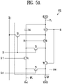
- FIGS. 5a and 5b are circuit diagrams illustrating an electrical connection relationship of components included in one pixel shown in FIG. 4 according to an embodiment.
- FIGS. 5a and 5b not only components included in each of the pixels shown in FIG. 4 but also an area in which the components are provided are collectively referred to as the pixel PXL.
- the pixel PXL shown in each of FIGS. 5a and 5b may be any one of the pixels PXL included in the display panel DP of FIG. 4 , and the pixels PXL may have structures substantially identical to or similar to each other.
- one pixel PXL may include an organic light emitting diode as the light emitting element LD.
- one pixel PXL may include a plurality of ultra-small inorganic light emitting diodes as small as a micro-scale or a nano-scale formed in a structure in which a nitride-based semiconductor is grown as the light emitting element LD.
- one active-type pixel PXL which is connected to an i-th scan line Si and an i-th emission control line Ei disposed in an i-th row (or pixel row) of the display area DA of the display panel DP and a j-th data line Dj disposed in a j-th column (or pixel column) and includes seven transistors and one storage capacitor Cst, is shown.
- each pixel PXL may include the light emitting element LD and a pixel circuit 144 for driving the light emitting element LD.
- the light emitting element LD may be an organic light emitting diode, but the present disclosure is not limited thereto.
- the pixel circuit 144 may be connected to a scan line Si and a data line Dj of a corresponding pixel PXL.
- the pixel circuit 144 of the pixel PXL may be connected to the i-th scan line Si and the j-th data line Dj of the display area DA.
- the pixel circuit 144 may be further connected to at least another scan line.
- one pixel PXL disposed in the i-th row of the display area DA of the display panel DP may be further connected to an (i-1)-th scan line Si-1 and/or an (i+1)-th scan line Si+1.
- the pixel circuit 144 may be further connected to a third power in addition to first and second pixel powers ELVDD and ELVSS.
- the pixel circuit 144 may also be connected to the initialization power Vint.
- the pixel circuit 144 may include first to seventh transistors T1 to T7 and a storage capacitor Cst.
- One electrode for example, a source electrode of the first transistor T1 (driving transistor) may be connected to a power line PL to which the first pixel power ELVDD is applied via the fifth transistor T5, and another electrode, for example, a drain electrode may be connected to the light emitting elements LD via the sixth transistor T6.
- a gate electrode of the first transistor T1 may be connected to a first node N1. The first transistor T1 may control a driving current flowing between the first pixel power ELVDD and the second pixel power ELVSS via the light emitting element LD in response to a voltage of the first node N1.
- the second transistor T2 (switching transistor) may be connected between the j-th data line Dj connected to the pixel PXL and the source electrode of the first transistor T1.
- a gate electrode of the second transistor T2 may be connected to the i-th scan line Si connected to the pixel PXL.
- the second transistor T2 may be turned on when a scan signal of a gate-on voltage (for example, a low voltage) is supplied from the i-th scan line Si, to electrically connect the j-th data line Dj to the source electrode of the first transistor T1. Therefore, when the second transistor T2 is turned on, the data signal supplied from the j-th data line Dj may be transmitted to the first transistor T1.
- a gate-on voltage for example, a low voltage
- the third transistor T3 may be connected between the drain electrode of the first transistor T1 and the first node N1.
- a gate electrode of the third transistor T3 may be connected to the i-th scan line Si.
- the gate electrode of the third transistor T3 may be turned on when the scan signal of the gate-on voltage is supplied from the i-th scan line Si, to electrically connect the drain electrode of the first transistor T1 and the first node N1 to each other.
- the fourth transistor T4 may be connected between the first node N1 and an initialization power line IPL to which the initialization power Vint is applied.
- a gate electrode of the fourth transistor T4 may be connected to a previous scan line, for example, the (i-1)-th scan line Si-1.
- the fourth transistor T4 may be turned on when the scan signal of the gate-on voltage is supplied to the (i-1)-th scan line Si-1, to transmit a voltage of the initialization power Vint to the first node N1.
- the initialization power Vint may have a voltage equal to or less than the lowest voltage of the data signal.
- the fifth transistor T5 may be connected between the power line PL to which the first pixel power ELVDD is applied and the first transistor T1.
- a gate electrode of the fifth transistor T5 may be connected to a corresponding emission control line, for example, an i-th emission control line Ei.
- the fifth transistor T5 may be turned off when an emission control signal of a gate-off voltage is supplied to the i-th emission control line Ei, and may be turned on in other cases.
- the sixth transistor T6 may be connected between the first transistor T1 and the light emitting element LD.
- a gate electrode of the sixth transistor T6 may be connected to the i-th emission control line Ei.
- the sixth transistor T6 may be turned off when the emission control signal of the gate-off voltage is supplied to the i-th emission control line Ei, and may be turned on in other cases.
- the seventh transistor T7 may be connected between the light emitting element LD and the initialization power line IPL to which the initialization power Vint is applied.
- a gate electrode of the seventh transistor T7 may be connected to any one of scan lines of a next stage, for example, the (i+1)-th scan line Si+1.
- the seventh transistor T7 may be turned on when the scan signal of the gate-on voltage is supplied to the (i+1)-th scan line Si+1, to supply the voltage of the initialization power Vint to the light emitting element LD.
- the signal applied to the gate electrode of the seventh transistor T7 may be a signal of the same timing as the scan signal of the gate on-voltage supplied to the i-th scan line Si.
- the storage capacitor Cst may be connected between the power line PL to which the first pixel power ELVDD is applied and the first node N1.
- the storage capacitor Cst may store a data signal and a voltage corresponding to a threshold voltage of the first transistor T1.
- a first electrode (or an anode electrode) of the light emitting element LD may be connected to the first transistor T1 via the sixth transistor T6, and a second electrode (or a cathode electrode) may be connected to the second pixel power ELVSS.
- the light emitting element LD generates light (or rays) of a predetermined luminance in response to a current amount supplied from the first transistor T1.
- a voltage value of the first pixel power ELVDD may be set higher than a voltage value of the second pixel power ELVSS so that a current may flow to the light emitting element LD.
- the light emitting element LD may be, for example, an organic light emitting diode.
- the light emitting element LD may emit light in one of red, green, and blue.
- the present disclosure is not limited thereto.
- each pixel PXL is not limited to the embodiment shown in FIG. 5a .
- the pixel circuits 144 of various currently known structures may be applied to each pixel PXL.
- each pixel PXL including a plurality of light emitting elements LD formed in a structure in which a nitride-based semiconductor is grown is described with reference to FIG. 5b .
- each pixel PXL may include a light emitting unit EMU that generates light of a luminance corresponding to the data signal.
- each pixel PXL may selectively further include the pixel circuit 144 for driving the light emitting unit EMU.
- the light emitting unit EMU may include a plurality of light emitting elements LD connected in parallel between a first power line PL1 to which a voltage of first driving power VDD is applied and a second power line PL2 to which second driving power VSS is applied.
- the light emitting unit EMU may include a first electrode EL1 (or a first alignment electrode) connected to the first driving power VDD via the pixel circuit 144 and the first power line PL1, a second electrode EL2 (or a second alignment electrode) connected to the second driving power VSS through the second power line PL2, and a plurality of light emitting elements LD connected in parallel in the same direction between the first and second electrodes EL1 and EL2.
- the first electrode EL1 may be an anode electrode
- the second electrode EL2 may be a cathode electrode.
- Each of the light emitting elements LD included in the light emitting unit EMU may include first and second semiconductor layers (not shown) formed of different types of semiconductor layers, and an active layer (not shown) interposed therebetween.
- each of the light emitting elements LD may be implemented as a light emitting stack in which the first semiconductor layer, the active layer, and the second semiconductor layer are sequentially stacked in one direction.
- the first semiconductor layer may be an n-type semiconductor layer
- the second semiconductor layer may be a p-type semiconductor layer.
- Each of the light emitting elements LD may include a first end connected to the first driving power VDD through the first electrode EL1 and a second end connected to the second driving power VSS through the second electrode EL2.
- the first driving power VDD and the second driving power VSS may have different potentials.
- the first driving power VDD may be set as high potential power
- the second driving power VSS may be set as low potential power.
- a potential difference between the first and second driving power VDD and VSS may be set to be greater than or equal to a threshold voltage of the light emitting elements LD during an emission period of the pixel PXL.
- each light emitting element LD connected in parallel in the same direction (for example, a forward direction) between the first electrode EL1 and the second electrode EL2 to which voltages of different potentials are respectively supplied may configure each effective light source.
- Such effective light sources may be gathered to configure the light emitting unit EMU of the pixel PXL.
- the light emitting elements LD of the light emitting unit EMU may emit light with a luminance corresponding to the driving current supplied through the pixel circuit 144.
- the pixel circuit 144 may supply a driving current corresponding to a grayscale value of corresponding frame data to the light emitting unit EMU.
- the driving current supplied to the light emitting unit EMU may be divided and may flow through the light emitting elements LD. Accordingly, the light emitting unit EMU may emit light of a luminance corresponding to the driving current while each light emitting element LD emits light with a luminance corresponding to the current flowing therethrough.
- the light emitting unit EMU may further include at least one ineffective light source in addition to the light emitting elements LD configuring each effective light source.
- at least a reverse light emitting element LDr may be further connected between the first and second electrodes EL1 and EL2 of the light emitting unit EMU.
- the reverse light emitting element LDr may be connected in parallel between the first and second electrodes EL1 and EL2 together with the light emitting elements LD configuring the effective light sources, and may be connected between the first and second electrodes EL1 and EL2 in a direction opposite to the light emitting elements LD.
- the pixel circuit 144 may be connected to the scan line Si and the data line Dj of the corresponding pixel PXL. For example, when the pixel PXL is disposed in the i-th (i is a natural number) row and the j-th (j is a natural number) column of the display area DA, the pixel circuit 144 of the pixel PXL may be connected to the i-th scan line Si and the j-th data line Dj of the display area DA. In addition, the pixel circuit 144 may be further connected to a control line CLi and a sensing line SENj of the pixel PXL.
- the pixel circuit 144 may include first to third transistors T1 to T3 and a storage capacitor Cst.
- first and second transistors T1 and T2 are similar to those of the first and second transistors T1 and T2 described with reference to FIG. 5A except for a connection position change of some components due to a type change of a transistor, a description thereof is omitted.
- the third transistor T3 is connected between the first transistor T1 and the sensing line SENj.
- one electrode of the third transistor T3 may be connected to one terminal (for example, the source electrode) of the first transistor T1 connected to the first electrode EL1, and another electrode of the third transistor T3 may be connected to the sensing line SENj. Meanwhile, when the sensing line SENj is omitted, a gate electrode of the third transistor T3 may be connected to the j-th data line Dj.
- the gate electrode of the third transistor T3 is connected to the control line CLi. Meanwhile, when the control line CLi is omitted, the gate electrode of the third transistor T3 may be connected to the i-th scan line Si.
- the third transistor T3 may be turned on by a control signal of a gate-on voltage (for example, a high level) supplied to the control line CLi during a predetermined sensing period, to electrically connect the sensing line SENj and the first transistor T1 to each other.
- a gate-on voltage for example, a high level
- a sensing period may be a period for extracting characteristic information (for example, the threshold voltage or the like of the first transistor T1) of each of the pixels PXL disposed in the display area DA.
- the first transistor T1 may be turned on by supplying a predetermined reference voltage at which the first transistor T1 may be turned on to the first node N1 through the j-th data line Dj and the second transistor T2, or connecting each pixel PXL to a current source or the like.
- the first transistor T1 may be connected to the sensing line SENj by supplying the control signal of the gate-on voltage to the third transistor T3 to turn on the third transistor T3.
- the characteristic information of each pixel PXL including the threshold voltage or the like of the first transistor T1 may be extracted through the above-described sensing line SENj.
- the extracted characteristic information may be used to convert image data so that a characteristic deviation between the pixels PXL is compensated.
- FIG. 5b discloses an embodiment in which all of the first to third transistors T1 to T3 are N-type transistors, but the present disclosure is not limited thereto. For example, at least one of the above-described first to third transistors T1 to T3 may be changed to a P-type transistor.
- FIG. 5b discloses an embodiment in which the light emitting unit EMU is connected between the pixel circuit 144 and the second driving power VSS, but the light emitting unit EMU may also be connected between the first driving power VDD and the pixel circuit 144.
- each pixel PXL applicable to the present disclosure is not limited to the embodiments shown in FIGS. 5a and 5b , and the corresponding pixel PXL may have various structures.
- FIG. 6 is a cross-sectional view taken along a line I ⁇ I' of FIG. 4
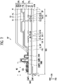
- FIGS. 7 to 9 are cross-sectional views corresponding to the line I ⁇ I' of FIG. 4 , which illustrates one area of the display panel shown in FIG. 6 in more detail.
- FIGS. 6 to 9 a structures of the dummy unit DMP and the pixel unit PX (or the display unit) are simplified, such as showing each electrode as a single electrode layer and each insulating layer as only a single insulating layer, but the present disclosure is not limited thereto.
- formed and/or provided on the same layer may mean formed in the same process, and “formed and/or provided on different layers” may mean formed in different processes.
- connection between two components may mean that both an electrical connection and a physical connection are used inclusively.
- the display panel DP may include the pixel unit PX or (the display unit) provided in the display area DA and the dummy unit DMP provided in the non-display area DA.
- the display panel DP may include a dam unit DAM provided in the non-display area DA and positioned between the dummy unit DMP and the pixel unit PX (or the display unit).
- the pixel unit PX (or the display unit) may include the pixels PXL provided on the substrate SUB and the thin film encapsulation layer TFE covering the pixels PXL.
- Each of the pixels PXL may include the pixel circuit layer PCL provided on the substrate SUB and the display element layer DPL provided on the pixel circuit layer PCL.
- the pixel circuit layer PCL may include a buffer layer BFL, the pixel circuit 144 provided on the buffer layer BFL, and a protective layer PSV provided on the pixel circuit 144.
- the buffer layer BFL may be provided and/or formed on one surface UF (or an upper surface) of the substrate SUB.
- the buffer layer BFL may prevent an impurity from diffusing into a transistor T included in the pixel circuit 144.
- the buffer layer BFL may be an inorganic insulating layer including an inorganic material.
- the buffer layer BFL may include at least one of metal oxide such as silicon nitride (SiNx), silicon oxide (SiOx), silicon oxynitride (SiON), and aluminium oxide (AlOx).
- the buffer layer BFL may be provided as a single layer, or may be provided as multiple layers of at least a double layer. When the buffer layer BFL is provided as the multiple layers, each layer may be formed of the same material or may be formed of different materials.
- the buffer layer BFL may be omitted according to a material, a process condition, and the like of the substrate SUB.
- the pixel circuit 144 may include at least one transistor T.
- the transistor T may include a driving transistor Tdr that controls a driving current of the light emitting element LD and a switching transistor (not shown) electrically connected to the driving transistor Tdr.
- the present disclosure is not limited thereto, and the pixel circuit 144 may further include circuit elements performing another function in addition to the driving transistor Tdr and the switching transistor.
- the driving transistor Tdr and the switching transistor are collectively referred to, the driving transistor Tdr and the switching transistor are referred to as a transistor T or transistors T.
- the driving transistor Tdr may have the same configuration as the first transistor T1 described with reference to FIGS.
- the switching transistor may have the same configuration as the second transistor T2 described with reference to FIGS. 5a and 5b .
- the driving transistor Tdr and the switching transistor may have a structure substantially similar to or identical to each other. Accordingly, a description of the switching transistor is replaced with a description of the driving transistor Tdr.
- the driving transistor Tdr may include a semiconductor pattern SCL, a gate electrode GE, a first terminal SE, and a second terminal DE.
- the first terminal SE may be any one of a source electrode and a drain electrode
- the second terminal DE may be the other electrode.
- the first terminal SE is a source electrode
- the second terminal DE may be a drain electrode.
- the semiconductor pattern SCL may be provided and/or formed on the buffer layer BFL.
- the semiconductor pattern SCL may include a first contact area contacting the first terminal SE and a second contact area contacting the second terminal DE.
- An area positioned between the first contact area and the second contact area and overlapping the gate electrode GE may be a channel area of the driving transistor Tdr.
- the semiconductor pattern SCL may be a semiconductor pattern formed of polysilicon, amorphous silicon, oxide semiconductor, or the like.
- the channel area may be a semiconductor pattern that is not doped with an impurity, and may be an intrinsic semiconductor, but the present disclosure is not limited thereto. According to an embodiment, the channel area may be a semiconductor pattern doped with an impurity.
- the first contact area and the second contact area may be semiconductor patterns doped with an impurity.
- the gate electrode GE may be provided and/or formed on the semiconductor pattern SCL with a gate insulating layer GI interposed therebetween.
- the gate electrode GE may be provided and/or formed on the gate insulating layer GI.
- the gate electrode GE may be formed of at least one or a metal such as gold (Au), silver (Ag), aluminium (Al), molybdenum (Mo), chromium (Cr), titanium (Ti), nickel (Ni), neodymium (Nd), and copper (Cu), or an alloy of the metals.
- the gate electrode GE may be formed as a single layer, but is not limited thereto, and may be formed as multiple layers in which at least two or more of the metals and the alloys are stacked.
- the gate insulating layer GI may be provided and/or formed on the semiconductor layer SCL.
- the gate insulating layer GI may be an inorganic insulating layer including an inorganic material.
- the gate insulating layer GI may include at least one of metal oxide such as silicon nitride (SiNx), silicon oxide (SiOx), silicon oxynitride (SiON), and aluminum oxide (AlOx).
- the material of the gate insulating layer GI is not limited to the above-described embodiments.
- the gate insulating layer GI may be formed of an organic insulating layer including an organic material.
- the gate insulating layer GI may be provided as a single layer, but may also be provided as multiple layers of at least double layers.
- the respective first terminal SE and second terminal DE may be in contact with the first contact area and the second contact area of the semiconductor pattern SCL through a contact hole passing through an interlayer insulating layer ILD and the gate insulating layer GI.
- the first terminal SE may be in contact with one contact area of the first and second contact areas of the semiconductor pattern SCL
- the second terminal DE may be in contact with a remaining contact area of the first and second contact areas of the semiconductor pattern SCL.
- the first and second terminals SE and DE may be formed of at least one of a metal such as gold (Au), silver (Ag), aluminium (Al), molybdenum (Mo), chromium (Cr), nickel (Ni), neodymium (Nd), and copper (Cu), or an alloy of the metals.
- a metal such as gold (Au), silver (Ag), aluminium (Al), molybdenum (Mo), chromium (Cr), nickel (Ni), neodymium (Nd), and copper (Cu), or an alloy of the metals.
- the first and second terminals SE and DE may be formed of a single layer, but are not limited thereto, and may be formed of multiple layers in which at least two or more of the metals and the alloys are stacked.
- the interlayer insulating layer ILD may be provided and/or formed on the gate electrode GE.
- the interlayer insulating layer ILD may be an inorganic insulating layer including an inorganic material.
- the interlayer insulating layer ILD may include at least one of a metal oxide such as silicon oxide (SiOx), silicon nitride (SiNx), silicon oxynitride (SiON), and aluminium oxide (AlOx).
- the interlayer insulating layer ILD may be formed of a single layer or multiple layers.
- the interlayer insulating layer ILD may be an organic insulating layer including an organic material.
- the first and second terminals SE and DE of the driving transistor Tdr are separate electrodes electrically connected to the semiconductor pattern SCL through a contact hole passing through the gate insulating layer GI and the interlayer insulating layer ILD, but the present disclosure is not limited thereto.
- the first terminal SE of the driving transistor Tdr may be one contact area of the first and second contact areas adjacent to the channel area of the semiconductor pattern SCL
- the second terminal DE of the driving transistor Tdr may be a remaining contact area of the first and second contact areas adjacent to the channel area of the semiconductor pattern SCL.
- the second terminal DE of the driving transistor Tdr may be electrically connected to the light emitting element LD of each pixel PXL through a separate connection means including a bridge electrode or a contact electrode.
- a sub-interlayer insulating layer (not shown) may be provided and/or formed on the first and second terminals SE and DE of the driving transistor Tdr.
- a first additional electrode (not shown, or a first connection electrode) corresponding to the first terminal SE and a second additional electrode (not shown, or a second connection electrode) corresponding to the second terminal DE may be provided and/or formed on the sub-interlayer insulating layer.
- the first additional electrode (or the first connection electrode) may be electrically connected to the first terminal SE disposed thereunder through a contact hole passing through the sub-interlayer insulating layer
- the second additional electrode (or the second connection electrode) may be electrically connected to the second terminal DE disposed thereunder through a contact hole passing through the sub-interlayer insulating layer.
- the transistors T included in the pixel circuit 144 may be configured of LTPS thin film transistors, but the present disclosure is not limited thereto, and may be configured of an oxide semiconductor thin film transistor according to an embodiment.
- the transistors T are thin film transistors having a top gate structure is described as an example, but the present disclosure is not limited thereto.
- the transistors T may be thin film transistors having a bottom gate structure.
- the protective layer PSV may be provided and/or formed on the pixel circuit 144 including the driving transistor Tdr.
- the protective layer PSV may be provided in a form including an organic insulating layer, an inorganic insulating layer, or an organic insulating layer disposed on the inorganic insulating layer.
- the inorganic insulating layer may include, for example, at least one of metal oxide such as silicon oxide (SiOx), silicon nitride (SiNx), silicon oxynitride (SiON), and aluminium oxide (AlOx).
- the organic insulating layer may include, for example, at least one of an acrylic resin (polyacrylates resin), an epoxy resin, a phenolic resin, a polyamide resin, a polyimides resin, an unsaturated polyesters resin, a poly-phenylene ethers resin, a polyphenylene sulfides resin, and a benzocyclobutene resin.
- the display element layer DPL may be provided and/or formed on the protective layer PSV.
- the display element layer DPL may be provided on the protective layer PSV and may include the light emitting element LD that emits light.
- the light emitting element LD may include first and second electrodes AE and CE and an emission layer EML provided between the two electrodes AE and CE.
- one of the first and second electrodes AE and CE may be an anode electrode, and a remaining electrode may be a cathode electrode.
- the first electrode AE may be a reflective electrode
- the second electrode CE may be a transmissive electrode.
- a case in which the light emitting element LD is the front surface emission type organic light emitting diode and the first electrode AE is the anode electrode is described as an example.
- the first electrode AE may be electrically connected to the second terminal DE of the driving transistor Tdr through a contact hole passing through the protective layer PSV.
- the first electrode AE may include a reflective layer (not shown) capable of reflecting light or a transparent conductive layer (not shown) disposed on or under the reflective layer.
- the first electrode AE may be configured of multiple layers including a lower transparent conductive layer formed of indium tin oxide (ITO), a reflective layer provided on the lower transparent conductive layer and formed of silver (Ag), and an upper transparent conductive layer provided on the reflective layer and formed of indium tin oxide (ITO). At least one of the transparent conductive layer and the reflective layer may be electrically connected to the second terminal DE of the driving transistor Tdr.
- the display element layer DPL may further include a pixel defining layer PDL having an opening exposing a portion of the first electrode AE, for example, an upper surface of the first electrode AE.
- the pixel defining layer PDL may be an organic insulating layer including an organic material.
- the pixel defining layer PDL may be formed of an organic insulating layer such as an acryl resin, an epoxy resin, a phenolic resin, a polyamide resin, or a polyimide resin.
- the emission layer EML may be disposed in an area corresponding to the opening of the pixel defining layer PDL. That is, the emission layer EML may be disposed on one surface of the exposed first electrode AE.
- the emission layer EML may have a multilayer thin film structure including at least a light generation layer.
- the emission layer EML may include a hole injection layer that injects a hole, a hole transport layer having an excellent hole transport property and for increasing a chance of recombination of a hole and an electron by suppressing a movement of an electron that is not combined in the light generation layer, the light generation layer that emits light by the recombination of the injected electron and hole, a hole blocking layer for suppressing a movement of a hole that is not combined in the light generation layer, an electron transport layer for smoothly transporting the electron to the light generation layer, and an electron injection layer for injecting the electron.
- a color of the light generated in the light generating layer may be one of red, green, blue, and white, but the present embodiment is not limited thereto.
- the color of the light generated in the light generating layer of the emission layer EML may be one of magenta, cyan, and yellow.
- the hole injection layer, the hole transport layer, the hole blocking layer, the electron transport layer, and the electron injection layer may be a common layer connected in emission areas adjacent to each other.
- the second electrode CE may be provided and/or formed on the emission layer EML.
- the second electrode CE may be a common layer commonly provided to the pixels PXL, but the present disclosure is not limited thereto.
- the second electrode CE may be a transmissive electrode and may include a transparent conductive material (or substance).
- the transparent conductive material (or substance) may include transparent conductive oxide such as indium tin oxide (ITO), indium zinc oxide (IZO), zinc oxide (ZnO), and indium tin zinc oxide (ITZO), a conductive polymer such as PEDOT, and the like.
- the thin film encapsulation layer TFE may be provided and/or formed on the second electrode CE.
- the thin film encapsulation layer TFE may be formed of a single layer, but may also be formed of multiple layers.
- the thin film encapsulation layer TFE may include a plurality of insulating layers covering the light emitting element OLED.
- the thin film encapsulation layer TFE may include at least one inorganic layer and at least one organic layer.
- the thin film encapsulation layer TFE may have a structure in which an inorganic layer and an organic layer are alternately stacked.
- the thin film encapsulation layer TFE may be an encapsulation substrate disposed on the light emitting element OLED and bonded to the substrate SUB through a sealant.
- the thin film encapsulation layer TFE may include first to third encapsulation layers ENC1 to ENC3.
- the first encapsulation layer ENC1 may be provided and/or formed on the display element layer DPL and may be positioned over at least a portion of the display area DA and the non-display area NDA.
- the second encapsulation layer ENC2 may be provided and/or formed on the first encapsulation layer ENC1 and may be positioned over at least a portion of the display area DA and the non-display area NDA.
- the third encapsulation layer ENC3 may be provided and/or formed on the second encapsulation layer ENC2 and may be positioned over at least a portion of the display area DA and the non-display area NDA.
- the third encapsulation layer ENC3 may be positioned over the entire display area DA and non-display area NDA.
- the first and third encapsulation layers ENC1 and ENC3 may be formed of an inorganic layer including an inorganic material
- the second encapsulation layer ENC2 may be formed of an organic layer including an organic material.
- the display element layer DPL includes the light emitting element LD configured of the front surface emission type organic light emitting diode having the first electrode AE, the emission layer EML, and the second electrode CE is described, but the present disclosure is not limited thereto.
- the display element layer DPL may include at least one ultra-small inorganic light emitting element LD (or light emitting diode) as small as a micro-scale or a nano-scale formed in a structure in which a nitride-based semiconductor is grown.
- the display element layer DPL may include first and second bank patterns BNK1 and BNK2, first and second alignment electrodes EL1 and EL2, and first and second insulating layers INS1 and INS2, and first and second contact electrodes CNE1 and CNE2.
- the light emitting element LD may have the same configuration as each light emitting element LD described with reference to FIG. 5B , and may replace each of the plurality of light emitting elements LD.
- the first bank pattern BNK1 may be provided and/or formed on the protective layer PSV, and may be positioned in the emission area from which light is emitted from each pixel PXL.
- the first bank pattern BNK1 may support each of the first and second alignment electrodes EL1 and EL2 in order to change a surface profile (or shape) of each of the first and second alignment electrodes EL1 and EL2 to guide the light emitted from the light emitting elements LD in an image display direction of the display device DD.
- the first bank pattern BNK1 may include an inorganic insulating layer formed of an inorganic material or an organic insulating layer formed of an organic material.
- the first bank pattern BNK1 may include an organic insulating layer of a single layer and/or an inorganic insulating layer of a single layer, but the present disclosure is not limited thereto.
- the second bank pattern BNK2 may surround at least one side of a peripheral area of each pixel PXL.
- the peripheral area may include a non-emission area from which light is not emitted.
- the second bank pattern BNK2 may be a structure defining (or partitioning) the emission area of each of the pixels PXL, and may be, for example, a pixel defining layer PDL.
- the second bank pattern BNK2 may include at least one light blocking material and/or reflective material to prevent a light leakage defect in which light (or rays) is leaked between the pixels PXL.
- Each of the first and second alignment electrodes EL1 and EL2 may be provided and/or formed on the first bank pattern BNK1 to have a surface profile corresponding to a shape of the first bank pattern BNK1.
- Each of the first and second alignment electrodes EL1 and EL2 may be formed of a material having a constant reflectance to allow the light emitted from each of the light emitting elements LD to proceed in the image display direction of the display device.
- the first alignment electrode EL1 may be electrically connected to the second terminal DE of the driving transistor Tdr through a contact hole passing through the protective layer PSV, and the second alignment electrode EL2 may be electrically and/or physically connected to a connection electrode E_CNT positioned in the non-display area NDA.
- the first alignment electrode EL1 may be an anode electrode
- the second alignment electrode EL2 may be a cathode electrode.
- the first alignment electrode EL1 may be a configuration corresponding to the first electrode AE described with reference to FIG. 7
- the second alignment electrode EL2 may be a configuration corresponding to the second electrode CE described with reference to FIG. 7 .
- the light emitting elements LD may be disposed between the first alignment electrode EL1 and the second alignment electrode EL2 and may be electrically connected to each of the first and second alignment electrodes EL1 and EL2. Each of the light emitting elements LD may emit any one of color light and/or white light.
- the light emitting elements LD may be provided in a form of being sprayed into a solution and may be injected into each pixel PXL.
- Each of the light emitting elements LD may include an emission stack pattern in which a first semiconductor layer 11, an active layer 12, and a second semiconductor layer 13 are sequentially stacked along one direction, for example, the first direction DR1.
- each of the light emitting elements LD may include an insulating layer (not shown) surrounding an outer circumferential surface of the emission stack pattern.
- the first semiconductor layer 11 may include at least one n-type semiconductor layer.
- the first semiconductor layer 11 may include a semiconductor material of any one of InAIGaN, GaN, AIGaN, InGaN, AIN, and InN, and may be an n-type semiconductor layer doped with a first conductive dopant (or an n-type dopant) such as Si, Ge, or Sn.
- the active layer 12 may be disposed on the first semiconductor layer 11 and may be formed in a single or multiple quantum well structure.
- the second semiconductor layer 13 may be disposed on the active layer 12, and may include a semiconductor layer of a type different from that of the first semiconductor layer 11.
- the second semiconductor layer 13 may include at least one p-type semiconductor layer.
- the second semiconductor layer 13 may include at least one semiconductor material of InAIGaN, GaN, AIGaN, InGaN, AIN, and InN, and may include a p-type semiconductor layer doped with a second conductive dopant (or a p-type dopant) such as Mg.
- the light emitting elements LD may be provided and/or formed on the first insulating layer INS1.
- the first insulating layer INS1 may be provided and/or formed between each of the first and second alignment electrodes EL1 and EL2 and the protective layer PSV.
- the first insulating layer INS1 may fill a space between each of the light emitting elements LD and the protective layer PSV to stably support the light emitting elements LD.
- the first insulating layer INS1 may include an inorganic insulating layer formed of an inorganic material or an organic insulating layer formed of an organic material.
- the second insulating layer INS2 may be provided and/or formed on the light emitting elements LD.
- the second insulating layer INS2 may be provided and/or formed on each of the light emitting elements LD to cover a portion of an upper surface of each of the light emitting elements LD, and may expose both ends of each of the light emitting elements LD to the outside.
- the second insulating layer INS2 may further fix each of the light emitting elements LD.
- a gap or space
- the gap may be filled with the second insulating layer INS2.
- first alignment electrode EL1 On the first alignment electrode EL1, a first contact electrode CNE1 electrically and/or physically and stably connecting the first alignment electrode EL1 and one end of the both ends of each of the light emitting elements LD may be provided and/or formed.
- second alignment electrode EL2 On the second alignment electrode EL2, a second contact electrode CNE2 electrically and/or physically and stably connecting the second alignment electrode EL2 and a remaining end of the both ends of each of the light emitting elements LD may be provided and/or formed.
- the first and second contact electrodes CNE1 and CNE2 may be formed of various transparent conductive materials in order to allow the light emitted from each of the light emitting elements LD and reflected by the first and second alignment electrodes EL1 and EL2 to proceed in the image display direction of the display device without loss.
- some configurations included in the pixel unit PX may be disposed in the non-display area NDA.
- a portion of the pixel circuit layer PCL, a portion of the display element layer DPL, and the thin film encapsulation layer TFE may be disposed in the non-display area NDA.
- the driver included in the pixel circuit layer PCL and the line unit included in the pixel circuit layer PCL and connecting the driver and the pixels PXL may be positioned in the non-display area NDA.
- the driver may include at least one driving transistor SDV_T formed through the same process as the driving transistor Tdr of the pixel unit PX (or the display unit).
- the driving transistor SDV_T may include the semiconductor pattern SCL, the gate electrode GE, the source electrode SE, and the drain electrode DE.
- the line unit may include signal lines SDV_SL connecting the driver and the pixels PXL.
- the signal lines SDV_SL may be fan-out lines.
- a power electrode PWE receiving the second pixel power ELVSS or the second driving power VSS from the outside, and the connection electrode E_CNT connected to the power electrode PWE may be disposed.
- the connection electrode E_CNT may electrically connect the power electrode PWE and the second electrode CE of the light emitting element LD as shown in FIG. 7 .
- the connection electrode E_CNT may electrically connect the power electrode PWE and the second alignment electrode EL2 as shown in FIG. 8 .
- the connection electrode E_CNT may be formed through the same process as the first electrode AE configuring the light emitting element LD, and may include the same layer structure and the same material as the first electrode AE1.
- connection electrode E_CNT may be provided in the same layer as one conductive layer among conductive layers in the pixel circuit layer PCL in a range electrically connecting the power electrode PWE and the second electrode CE.
- the connection electrode E_CNT may be formed through the same process as the first and second alignment electrodes EL1 and EL2, and may include the same layer structure and the same material as the first and second alignment electrodes EL1 and EL2.
- the dam unit DAM may be provided along an edge of the display area DA, and may be positioned between the dummy unit DMP and the pixel unit PX (or the display unit) in the non-display area NDA.
- the dam unit DAM may include a first dam unit DAM1 and a second dam unit DAM2.
- the second dam unit DAM2 may be disposed outside the first dam unit DAM1.
- the first dam unit DAM1 may be formed simultaneously with the protective layer PSV included in the pixel circuit layer PCL.
- the second dam unit DAM2 may include a lower portion DAMP1 formed simultaneously with the protective layer PSV included in the pixel circuit layer PCL, and an upper portion DAMP2 formed simultaneously with the pixel defining layer PDL included in the display element layer DPL.
- the dam unit DAM is formed simultaneously with the organic insulating layers included in the pixel unit PX (or the display unit), but the present disclosure is not limited thereto. According to an embodiment, the dam unit DAM may be simultaneously formed with at least one insulating layer among inorganic insulating layers included in the pixel unit PX (or the display unit).
- the dam unit DAM may prevent a liquid organic material from overflowing into an outer area of the substrate SUB in a process of forming the organic layer included in the thin film encapsulation layer TFE, for example, the second encapsulation layer ENC2.
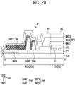
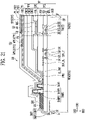
- the dummy unit DMP is positioned outside the dam unit DAM and may be provided along the edge (or the outer area) of the substrate SUB.
- the dummy unit DMP may include a first dummy pattern DMP1 and a second dummy pattern DMP2.
- the first dummy pattern DMP1 may be positioned between the substrate SUB and the pixel circuit layer PCL in the non-display area NDA.
- the first dummy pattern DMP1 may be positioned between the substrate SUB and the buffer layer BFL.
- the first dummy pattern DMP1 may be provided along the edge (or the outer area) of the substrate SUB, and may overlap the edge (or the outer area) of the substrate SUB.
- the first dummy pattern DMP1 may function as an etch stopper that prevents the substrate SUB from being excessively etched by an etching gas in a manufacturing process of the display device DD.
- the first dummy pattern DMP1 may be formed of a material (or a substance) with little (or less) effect by the etching gas in order to prevent a portion of the substrate SUB from being excessively etched when the mother substrate (or the mother substrate) is provided as the display panel DP of one cell unit by performing a dry etching method.
- the first dummy pattern DMP1 may include a transparent conductive material (or substance).
- the transparent conductive material (or substance) may include transparent conducting oxide (TCO) such as indium tin oxide (ITO), indium zinc oxide (IZO), zinc oxide (ZnO), or indium tin zinc oxide (ITZO).
- the second dummy pattern DMP2 may be positioned between the pixel circuit layer PCL and the display element layer DPL in the non-display area NDA.
- the second dummy pattern DMP2 may be provided on the first dummy pattern DMP1 and surround one end of the pixel circuit layer PCL in order to prevent the one end of the pixel circuit layer PCL positioned in the non-display area NDA from being exposed to the outside. That is, the second dummy pattern DMP2 may function as a protection member protecting the one end of the pixel circuit layer PCL.
- the second dummy pattern DMP2 may minimize damage of configurations disposed on one surface UF (or the upper surface) of the substrate SUB, for example, the buffer layer BFL and the insulating layers provided on the buffer layer BFL in the manufacturing process of the display device DD.
- the second dummy pattern DMP2 may be formed of a material (or substance) having a small (or less) influence by an etching gas used in a process of performing the dry etching method.
- the second dummy pattern DMP2 may include the same material (or substance) as the first dummy pattern DMP1.
- the second dummy pattern DMP2 may include a transparent conductive oxide.
- the second dummy pattern DMP2 may be formed in the same process as some configurations included in the display element layer DPL.
- the second dummy pattern DMP2 may be formed in the same process as the second electrode CE when the second electrode CE included in the display element layer DPL is configured of a transmissive electrode, and may include the same material as the second electrode CE.
- the present disclosure is not limited thereto, and according to an embodiment, the second dummy pattern DMP2 may be formed in a process different from that of the second electrode CE and may be provided on a layer different from that of the second electrode CE.
- the second dummy pattern DMP2 may be formed in the same process as the first and second contact electrodes CNE1 and CNE2 included in the display element layer DPL, and may include the same material as the first and second contact electrodes CNE1 and CNE2.
- the first dummy pattern DMP1 and the second dummy pattern DMP2 may overlap each other.
- the first and second dummy patterns DMP1 and DMP2 may extend along the first direction DR1 from an edge end A of the substrate SUB in the non-display area NDA and may be positioned in a range that does not overlap the dam unit DAM.
- the edge end A of the substrate SUB may be an edge where the one surface UF (or the upper surface) of the substrate SUB and a side surface, which connects the one surface UF (or the upper surface) and another surface BF (or a rear surface), contact.
- the present disclosure is not limited thereto, and positions of the first and second dummy patterns DMP1 and DMP2 may be variously changed within a range capable of ensuring electrical insulation from the driver disposed in the non-display area NDA.
- Each of the first and second dummy patterns DMP1 and DMP2 may maintain a state electrically separated from a configuration to which any signal (or voltage) is applied from the outside.
- each of the first and second dummy patterns DMP1 and DMP2 may maintain a state electrically separated from a configuration to which a predetermined signal (or voltage) is applied in the display device DD.
- a width W2 of the second dummy pattern DMP2 in the first direction DR1 and a width W1 of the first dummy pattern DMP1 in the first direction DR1 may be different from each other.
- the width W2 of the second dummy pattern DMP2 in the first direction DR1 may be greater than the width W1 of the first dummy pattern DMP1 in the first direction DR1, but the present disclosure is not limited thereto.
- the width W1 of the first dummy pattern DMP1 in the first direction DR1 may be greater than the width W2 of the second dummy pattern DMP2 in the first direction DR1.
- the width W2 of the second dummy pattern DMP2 in the first direction DR1 and the width W1 of the first dummy pattern DMP1 in the first direction DR1 may be identical to each other.
- the first and second dummy patterns DMP1 and DMP2 may protrude from the edge end A of the substrate SUB in a direction away from the pixel unit PX (or the display unit) in the first direction DR1.
- the first and second dummy patterns DMP1 and DMP2 may protrude outward from the edge end A of the substrate SUB. That is, the first and second dummy patterns DMP1 and DM2P may include a protrusion that does not overlap the substrate SUB and facing to the outside of the substrate SUB.
- an end of the protrusion of the first dummy pattern DMP1 and an end of the protrusion of the second dummy pattern DMP2 may coincide with each other.
- a width d of the protrusion of the first dummy pattern DMP1 in the first direction DR1 and a width d of the protrusion of the second dummy pattern DMP2 in the first direction DR1 may be identical to each other.
- the width d of each of the first and second dummy patterns DMP1 and DMP2 in the first direction DR1 may be about 0 ⁇ m to 5 ⁇ m, but the present disclosure is not limited thereto.
- the width d of the first dummy pattern DMP1 in the first direction DR1 and the width d of the second dummy pattern DMP2 in the first direction DR1 are identical to each other, but the present disclosure is not limited thereto.
- the width d of the protrusion of the first dummy pattern DMP1 in the first direction DR1 and the width d of the protrusion of the second dummy pattern DMP2 in the first direction DR1 may be different from each other.
- a portion of the substrate SUB may be removed in a process of manufacturing the mother substrate (not shown, or the mother substrate) in one display panel DP, and thus the first and second dummy patterns DMP1 and DMP2 may protrude outward from the edge end A of the substrate SUB.
- a light blocking layer LBL may be disposed in the non-display area NDA.
- the light blocking layer LBL may be disposed between the first dummy pattern DMP1 and the second dummy pattern DMP2.
- the light blocking layer LBL may be provided on the interlayer insulating layer IDL provided in the pixel circuit layer PCL positioned in the non-display area NDA and may be disposed between the first dummy pattern DMP1 and the second dummy pattern DMP2, but the present disclosure is not limited thereto.
- the light blocking layer LBL may be provided on one insulating layer among the insulating layers included in the pixel circuit layer PCL positioned in the non-display area NDA or may be provided on one insulating layer among the insulating layers included in the display element layer DPL positioned in the non-display area NDA.
- the light blocking layer LBL may be a visibility preventing member that prevents the first and second dummy patterns DMP1 and DMP2 from being easily identified by a user.
- the light blocking layer LBL may be formed of a material (or substance) that has a certain level of dielectric constant and absorbs and/or blocks light.
- the light blocking layer LBL may include a black matrix.
- the display panel DP when the display device DD is manufactured with a large area, the display panel DP is manufactured by tiling, and at this time, in order to minimize a distance between adjacent display panels DP, a portion or the entire driver positioned in the non-display area NDA may be positioned on the other surface BF (or the rear surface) of the substrate SUB of the corresponding display panel DP.
- the portion or the entire driver may be positioned on an insulating layer (not shown) positioned on the other surface BF (or the rear surface) of the substrate SUB, and may be electrically connected to a conductive layer of the pixel circuit layer PCL positioned on the one surface UF (or the upper surface) of the substrate SUB through a contact hole passing through the substrate SUB and the insulating layer.
- an auxiliary layer ADL may be disposed in the non-display area NDA as shown in FIG. 9 .
- the auxiliary layer ADL may be provided and/or formed between the light blocking layer LBL and the second dummy pattern DMP2.
- the auxiliary layer ADL may be a member that diffuses and/or scatters light entering from the outside in order to additionally prevent visibility of the first and second dummy patterns DMP1 and DMP2.
- the auxiliary layer ADL may be formed of a diffusion ink material having a reflectance of a constant level or more.
- the diffusion ink material may be formed by including, for example, a polystyrene (PS) or polymethylmethacrylate (PMMA) bead, a solvent, a polystyrene (PS) or polymethacrylate (PMMA) copolymer, and an addition agent, but the present disclosure is not limited thereto.
- the auxiliary layer ADL may include a polymer material having light transmittance.
- the polymer material may include polyethylene terephthalate, polyethylene naphthalate, polycarbonate, and polymethyl methacrylate.
- the material (or substance) of the auxiliary layer ADL is not limited to the above-described embodiments, and may be variously selected among materials (or substances) capable of easily diffusing and/or scattering light entering from the outside.
- the auxiliary layer ADL may include fine particles DFP.
- the auxiliary layer ADL may include fine particles DFP for light diffusion and/or light scattering by being dispersed in a medium such as a transparent binder.
- the fine particles DFP may be referred to as diffusion particles, scattering particles, or the like.
- the fine particles DFP may have a size of several tens nm to several ⁇ m, but the present disclosure is not limited thereto.
- the binder may include a transparent material such as acrylic, urethane, or epoxy resin. As the fine particles DFP, a transparent particle or a white particle may be used.
- the transparent particle may be, for example, a transparent organic particle or inorganic particle.
- the organic particle may include methyl methacrylate (MMA), acrylic acid, glycidyl methacrylate, ethyl acrylate (EA), isobutyl acrylate, normal butyl acrylate, an acrylic particle of 2-ethyhexyl acrylate homopolymer or copolymer, an olefin-based particle such as polyethylene, polystyrene, and polypropylene, an acrylic and olefinic copolymer particle, a multi-layered multi-component particle formed by forming a homopolymer particle and then covering a different type of monomer on the homopolymer particle, or the like.
- MMA methyl methacrylate
- EA ethyl acrylate
- isobutyl acrylate normal butyl acrylate
- an acrylic particle of 2-ethyhexyl acrylate homopolymer or copolymer an
- the inorganic particle may include, for example, precipitated silica, a glass bead, diamond, and the like.
- the white particle titanium oxide (TiO 2 ), zinc oxide (ZnO), barium sulfate (BaSO 4 ), calcium carbonate (CaCO 3 ), magnesium carbonate (MgCO 3 ), aluminium hydroxide (Al(OH) 3 ), clay, or the like may be used.
- the above-described transparent particle or white particle may be used alone or by mixing two or more types of the above-described transparent particle or white particle.
- fine particles DFP have been illustrated to have the same size, the present disclosure is not limited thereto. According to an embodiment, the fine particles DFP may have different sizes. In addition, although it is illustrated that the fine particles DFP are regularly distributed in the auxiliary layer ADL, the present disclosure is not limited thereto. According to an embodiment, the fine particles DFP may be irregularly distributed, such as being biasedly distributed toward one side in the auxiliary layer ADL.
- the auxiliary layer ADL may diffuse and/or scatter the light to disperse the light in various directions. Accordingly, the auxiliary layer ADL may minimize the visibility of the first and second dummy patterns DMP1 and DMP2 together with the light blocking layer LBL.
- damage of the configurations may be prevented by protecting the configurations positioned at the edge of the substrate SUB when proceeding a process of providing the mother substrate (or the mother substrate) in one display panel DP through a dry etching method by disposing the dummy unit DMP along the edge of the substrate SUB.
- a dead space of the non-display area NDA may be minimized because an extra space for preventing damage by a laser beam is not required to be secured, by applying the dry etching method instead of a cutting method using a laser beam when the mother substrate (or the mother substrate) is provided in one display panel DP unit.
- FIGS. 10a to 10d are schematic plan views sequentially illustrating a method of manufacturing a display device according to an embodiment of the present disclosure
- FIG. 11a is a cross-sectional view taken along a line II ⁇ II' of FIG. 10a
- FIG. 11b is a cross-sectional view taken along the line II ⁇ II' of FIG. 10b
- FIG. 11c is a cross-sectional view taken along the line II ⁇ II' of FIG. 10c
- FIG. 11d is a cross-sectional view taken along the line II ⁇ II' of FIG. 10d .
- FIGS. 6 and 7 are sequentially described according to a manufacturing method in conjunction with FIGS. 10a to 10d and 11a to 11d .
- a mother substrate MSUB is prepared.
- a carrier substrate (not shown) for supporting the mother substrate MSUB may be provided on a rear surface of the mother substrate MSUB.
- the mother substrate MSUB and the carrier substrate may be in contact with each other and may be attached with each other by static electricity or van der Waals force.
- the mother substrate MSUB may include at least one or more unit areas UNT1 and UNT2.
- the mother substrate MSUB may include a first unit area UNT1 and a second unit area UNT2.
- the unit areas UNT1 and UNT2 may be portions corresponding to an individual display panel DP or an individual display device DD, and the substrate SUB of the individual display panel DP or the individual display device DD may be formed for each of unit areas UNT1 and UNT2.
- the first unit area UNT1 and the second unit area UNT2 may have the same size (or area) and may be disposed in a matrix shape in the mother substrate MSUB, but the present disclosure is not limited thereto. According to an embodiment, the first unit area UNT1 and the second unit area UNT2 may have different sizes (or areas) in the mother substrate MSUB, and may be disposed in various shapes according to a size (or an area) of the mother substrate MSUB. In an embodiment of the present disclosure, each of the first unit area UNT1 and the second unit area UNT2 may include the display area DA and the non-display area NDA.
- the first unit area UNT1 and the second unit area UNT2 may be divided by a virtual line VL extending in the second direction DR2.
- the virtual line VL may partition one unit area UNT1 or UNT2 in a shape surrounding each of the first and second unit areas UNT1 and UNT2.
- the virtual line VL may be positioned between the first unit area UNT1 and the second unit area UNT2. Accordingly, at least one side of the first unit area UNT1 may be in contact with the second unit area UNT2 with the virtual line VL interposed therebetween.
- the mother substrate MSUB may be provided as a plurality of individual display panels DP along the virtual line VL.
- the first unit area UNT1 and the second unit area UNT2 adjacent to each other may contact each other or may be spaced apart from each other.
- the first unit area UNT1 and the second unit area UNT2 adjacent to each other are in contact with each other with one virtual line VL interposed therebetween, but the present disclosure is not limited thereto.
- the first unit area UNT1 and the second unit area UNT2 spaced apart from each other may be divided by two or more virtual lines VL.
- the first dummy pattern DMP1 is formed on one surface of the above-described mother substrate MSUB.
- the first dummy pattern DMP1 may be formed through a photo-lithography process using a mask, and may be positioned in the non-display area NDA of each of the first unit area UNT1 and the second unit area UNT2.
- the pixel unit PX (or the display unit), the driver, the line unit, the dam unit DAM, the light blocking layer LBL, and the second dummy pattern DMP2 are formed on the mother substrate MSUB on which the first dummy pattern DMP1 is disposed.
- the pixel unit PX (or the display unit) may include a plurality of pixels PXL provided in the display area DA in the first and second unit areas UNT1 and UNT2 and the thin film encapsulation layer TFE covering the pixels PXL.
- the thin film encapsulation layer TFE may be an encapsulation substrate covering the pixels PXL, the driver, the dam unit DAM, the light blocking layer LBL, and the second dummy pattern DMP2.
- the mother substrate MSUB may be a lower substrate and the thin film encapsulation layer TFE may be an upper substrate.
- Each of the pixels PXL may include the pixel circuit layer PCL provided on the substrate SUB and the display element layer DPL provided on the pixel circuit layer PCL.
- the pixels PXL and the like may be formed through various processes, and for example, may be formed using a plurality of depositions and/or photo-lithography.
- the second dummy pattern DMP2 may be positioned in the non-display area NDA of each of the first and second unit areas UNT1 and UNT2 and may be formed along an edge of the mother substrate MSUB.
- the second dummy pattern DMP2 may be formed in the non-display area NDA between the first unit area UNT1 and the second unit area UNT2 based on the virtual line VL.
- the virtual line VL may be disposed at a position that bisects the second dummy pattern DMP2 positioned in the non-display area NDA between the first unit area UNT1 and the second unit area UNT2 when viewed on a plane and a cross-section.
- One side and another side of the second dummy pattern DMP2 bisected by the virtual line VL may be included in the unit areas UNT1 and UNT2 adjacent to each other, respectively.
- the one side of the second dummy pattern DMP2 may be included in the first unit area UNT1
- the other side of the second dummy pattern DMP2 may be included in the second unit area UNT2.
- the second dummy pattern DMP2 may overlap the first dummy pattern DMP1.
- the second dummy pattern DMP2 may be formed of a transparent conductive oxide and may be manufactured in the same process as a partial configuration of the pixel unit PX (or the display unit).
- the second dummy pattern DMP2 may be manufactured in the same process as the second electrode CE of the display element layer DPL, and may include the same material as the second electrode CE.
- the present disclosure is not limited thereto, and according to an embodiment, the second dummy pattern DMP2 may be formed in a separate step different from that of the configurations of the display element layer DPL.
- the second dummy pattern DMP2 may be provided in a shape surrounding a partial configuration positioned in the non-display area NDA of each of the first and second unit areas UNT1 and UNT2.
- the second dummy pattern DMP2 may be provided in a shape surrounding one end of the pixel circuit layer PCL positioned in the non-display area NDA.
- a portion of the mother substrate MSUB is removed by performing a dry etching process by seating the above-described mother substrate MSUB in a vacuum chamber.
- the rear surface of the mother substrate MSUB may be an etch object surface, and one area corresponding to the display area DA of each of the first and second unit areas UNT1 and UNT2 may be covered by a mask.
- the partial configuration may be prevented from being damaged by an etching gas used in the dry etching process.
- the mother substrate MSUB may be prevented from being excessively etched by the etching gas.
- the substrate SUB from which a portion of the mother substrate MSUB is removed by the etching gas used in the dry etching process may be provided.
- the substrate SUB from which a portion is removed by the above-described process may have a side surface having an inverse tapered shape.
- a width of the substrate SUB may become narrower from the upper surface (refer to 'UF of FIG. 7 ) to the rear surface (refer to 'BF' of FIG. 7 ) along the first direction DR1.
- the substrate SUB may be a base substrate of each of the first and second unit areas UNT1 and UNT2, and may have the same configuration as the substrate SUB described with reference to FIGS. 4 and 7 .
- the first and second dummy patterns DMP1 and DMP2 may protrude formed from the edge end (refer to 'A' of FIG. 7 ) of the substrate SUB along the first direction DR1.
- the first and second dummy patterns DMP1 and DMP2 positioned adjacent to the virtual line VL may be separated based on the virtual line (refer to 'VL of FIG. 10c ), and thus the individual display panel DP may be provided.
- FIG. 12 is a cross-sectional view corresponding to the line I ⁇ I' of FIG. 4 as an implementation of the third encapsulation layer shown in FIG. 6 according to another embodiment
- FIG. 13 is a cross-sectional view corresponding to the line I ⁇ I' of FIG. 4 , which illustrates one area of the display panel shown in FIG. 12 in more detail.
- the display panel DP may include the substrate SUB, the pixel unit PX (or the display unit), the thin film encapsulation layer TFE, the dummy unit DMP, and the dam unit DAM.
- the pixel unit PX (or the display unit) may include the pixels PXL provided in the display area DA and the thin film encapsulation layer TFE covering the pixels PXL.
- the pixel unit PX (or the display unit) may include the pixel circuit layer PCL provided on the substrate SUB, the display element layer DPL provided on the pixel circuit layer PCL, and the thin film encapsulation layer TFE provided on the display element layer DPL.
- the display element layer DPL may include at least one light emitting element LD formed of an organic light emitting diode.
- the display element layer DPL may include at least one light emitting element LD formed of an inorganic light emitting diode as small as a microscale or a nano-scale formed in a structure in which a nitride-based semiconductor is grown as shown in FIGS. 5b and 8 .
- the display element layer DPL may further include the first and second bank patterns (refer to 'BNK1 and BNK2' of FIG. 8 ), the first and second alignment electrodes (refer to 'EL1 and EL2' of FIG. 8 ), the first and second insulating layers (refer to 'INS1 and INS2' of FIG. 8 ) and the first and second contact electrodes (refer to 'CNE1 and CNE2' of FIG. 8 ).
- the dummy unit DMP may include the first dummy pattern DMP1 and the second dummy pattern DMP2 provided in the non-display area NDA.
- the first dummy pattern DMP1 may be provided on the one surface UF (or the upper surface) of the substrate SUB, and may protrude from the edge end A of the substrate SUB in a direction away from the pixel unit PX (or the display unit) along the first direction DR1.
- the second dummy pattern DMP2 may be provided on the light blocking layer LBL and may cover side surfaces of some components positioned on the upper surface of the substrate SUB. Similarly to the first dummy pattern DMP1, the second dummy pattern DMP2 may protrude from the edge end A of the substrate SUB in a direction away from the pixel unit PX (or the display unit) along the first direction DR1.
- An insulating layer INS may be provided and/or formed on the second dummy pattern DMP2.
- the insulating layer INS may prevent the second dummy pattern DMP2 formed of a transparent conductive oxide from being exposed to the outside to protect the second dummy pattern DMP2.
- the insulating layer INS may be an inorganic insulating layer including an inorganic material.
- the insulating layer INS may include at least one of a metal oxide such as silicon nitride (SiNx), silicon oxide (SiOx), silicon oxynitride (SiON), or aluminium oxide (AlOx).
- the insulating layer INS may be provided integrally with a partial configuration of the thin film encapsulation layer TFE.
- the insulating layer INS may be formed of an inorganic layer in the thin film encapsulation layer TFE and may be provided integrally with the third encapsulation layer ENC3 corresponding to the uppermost layer (or outermost layer) of the display panel DP.
- the present disclosure is not limited thereto, and according to an embodiment, when the first encapsulation layer ENC1 formed of an inorganic layer in the thin film encapsulation layer TFE is provided up to the edge end A of the substrate SUB, the insulating layer INS may be provided integrally with the first encapsulation layer ENC1.
- the insulating layer INS disposed on the second dummy pattern DMP2 is provided integrally with a partial configuration of the thin film encapsulation layer TFE, but the present disclosure is not limited thereto. According to an embodiment, the insulating layer INS may be provided non-integrally with the thin film encapsulation layer TFE.
- FIG. 14 is a schematic plan view illustrating the display panel shown in FIG. 4 according to another embodiment
- FIG. 15 is a cross-sectional view taken along a line III ⁇ III' of FIG. 14 .
- the display panel DP may include the dummy unit DMP positioned along the edge of the substrate SUB.
- the dummy unit DMP may be positioned in the non-display area NDA of the substrate SUB.
- the dummy unit DMP may have a shape forming a closed circuit along the edge of the substrate SUB when viewed on a plane.
- the dummy unit DMP may include the first dummy pattern DMP1 and the second dummy pattern DMP2.
- the first dummy pattern DMP1 and the second dummy pattern DMP2 may have the same planar shape and overlap each other.
- a width W3 of the first dummy pattern DMP1 in the first direction DR1 and a width W3 of the second dummy pattern DMP2 in the first direction DR1 may be identical to each other.
- a width W4 of the first dummy pattern DMP1 in the second direction DR2 and a width W4 of the second dummy pattern DMP2 in the second direction DR2 may be identical to each other.
- the width W3 of each of the first and second dummy patterns DMP1 and DMP2 in the first direction DR1 and the width W4 of each of the first and second dummy patterns DMP1 and DMP2 in the second direction DR2 may be identical to each other, but the present disclosure is not limited thereto. According to an embodiment, the width W3 of each of the first and second dummy patterns DMP1 and DMP2 in the first direction DR1 may be greater than (or wider than) the width W4 of each of the first and second dummy patterns DMP1 and DMP2 in the second direction DR2 or vice versa.
- the above-described display device DD may include a touch sensor between the display panel DP and the window WD.
- the display device DD including the touch sensor is described.
- FIG. 16 is a schematic cross-sectional view illustrating the display device of FIG. 1 according to another embodiment
- FIG. 17 is a schematic cross-sectional view of the touch sensor of FIG. 16 .
- the display device DD may include a display module DM and the window WD.
- the display module DM may include the display panel DP and the touch sensor TS.
- the display panel DP may have the same configuration as the display panel DP described with reference to FIGS. 2 to 7 .
- the window WD may have the same configuration as the window WD described with reference to FIG. 2 , and may be coupled to the display module DM using an optically transparent viscosity (or adhesive) member OCA.
- the touch sensor TS may be directly disposed on a surface on which an image of the display panel DP is emitted to receive a user's touch input and/or a hover input.
- the touch sensor TS may sense a touch capacitance by contact and/or proximity of a separate input means such as a user's hand or a conductor similar thereto to recognize the touch input and/or the hover input of the display device DD.
- the touch input may mean a direct touch (or contact) by a user's hand or a separate input means
- the hover input may mean that a user's hand or a separate input means is near the display device DD including the touch sensor TS but does not touch the display device DD.
- the touch sensor TS may sense a user's touch operation and move an object displayed on the display device DD from an originally displayed position to another position in response to the touch operation.
- the touch operation may include at least one touch among one single touch, a multi-touch, and a touch gesture.
- various touch operations including a specific gesture such as enlarging or reducing text or an image by moving a predetermined distance in a state in which a user's finger touches on a touch surface of the touch sensor TS may exist.
- the touch sensor TS may have a multiple layer structure.
- the touch sensor TS may include at least one or more conductive layers and may include at least one or more insulating layers.
- the touch sensor TS may include a base layer BSL, a first conductive pattern CP1, a first touch insulating layer TS_INS1, a second conductive pattern CP2, and a second touch insulating layer TS_INS2.
- the first conductive pattern CP1 may be directly disposed on the thin film encapsulation layer TFE of the display panel DP, but the present disclosure is not limited thereto.
- another insulating layer for example, the base layer BSL, may be disposed between the first conductive pattern CP1 and the thin film encapsulation layer TFE.
- the first conductive pattern CP1 may be directly disposed on the base layer BSL.
- Each of the first and second conductive patterns CP1 and CP2 may have a single layer structure or may have a multiple layer structure stacked in a thickness direction, for example, the third direction DR3.
- the conductive pattern of the single layer structure may include a metal layer or a transparent conductive layer.
- the metal layer may include molybdenum (Mo), silver (Ag), titanium (Ti), copper (Cu), aluminum (Al), and an alloy thereof.
- the transparent conductive layer may include transparent conductive oxide such as indium tin oxide (ITO), indium zinc oxide (IZO), zinc oxide (ZnO), or indium tin zinc oxide (ITZO).
- the transparent conductive layer may include PEDOT, a metal nanowire, and graphene.
- the conductive pattern of the multiple layer structure may include metal layers of multiple layers.
- the metal layers of multiple layers may have, for example, a triple structure of titanium (Ti)/aluminium (Al)/titanium (Ti), but is not limited thereto.
- the conductive pattern of the multiple layer structure may include metal layers of multiple layers and a transparent conductive layer.
- each of the first and second conductive patterns CP1 and CP2 may include sensor patterns and sensing lines.
- Each of the first and second touch insulating layers TS_INS1 and TS_INS2 may include an inorganic insulating layer including an inorganic material or an organic insulating layer including an organic material.
- the inorganic insulating layer may include at least one of a metal oxide such as silicon nitride (SiNx), silicon oxide (SiOx), silicon oxynitride (SiON), and aluminium oxide (AlOx).
- the organic insulating layer may include at least one of acrylic resin, methacrylic resin, polyisoprene, vinyl-based resin, epoxy-based resin, urethane-based resin, cellulose-based resin, siloxane-based resin, polyimide-based resin, polyamide-based resin, and perylene-based resin.
- FIG. 18 is a schematic plan view of the touch sensor of FIG. 16
- FIG. 19a is an enlarged plan view schematically illustrating an example of a portion EA of FIG. 18
- FIG. 19b is a cross-sectional view taken along a line V ⁇ V' of FIG. 19a .
- the touch sensor TS may include a base layer BSL including a sensing area SA capable of sensing a touch input and a non-sensing area NSA surrounding at least a portion of the sensing area SA.
- the base layer BSL may be formed of tempered glass, transparent plastic, or a transparent film. According to an embodiment, the base layer BSL may be omitted.
- the sensing area SA may be provided in a central area of the base layer BSL to overlap the display area DA of the display panel DP.
- the sensing area SA may be provided in a shape substantially the same as that of the display area DA, but the present disclosure is not limited thereto.
- a sensor electrode for sensing the touch input may be provided and/or formed in the sensing area SA.
- the non-sensing area NSA may be provided in a peripheral area of the base layer BSL to overlap the non-display area NDA of the display panel DP.
- the peripheral area may be an area surrounding the central area of the base layer BSL.
- Sensing lines SL electrically connected to the sensor electrode to receive and transmit a sensing signal are provided and/or formed in the non-sensing area NSA.
- a pad unit PDA connected to the sensing lines SL and electrically connected to the sensor electrode of the sensing area SA may be disposed in the non-sensing area NSA.
- the pad unit PDA may include a plurality of pads PD.
- the sensing line SL may include a plurality of first sensing lines SL1 and a plurality of second sensing lines SL2.
- the sensor electrode may include a plurality of sensor patterns SP and first and second bridge patterns BRP1 and BRP2.
- the sensor patterns SP may include a plurality of first sensor patterns SP1 and a plurality of second sensor patterns SP2 electrically insulated from the first sensor patterns SP1.
- the first sensor patterns SP1 may be arranged in the first direction DR1 and may be electrically connected to the adjacent first sensor patterns SP1 by the first bridge patterns BRP1 to configure at least one sensor row.
- the second sensor patterns SP2 may be arranged in the second direction DR2 crossing the first direction DR1 and may be electrically connected to the adjacent second sensor patterns SP2 through the second bridge patterns BRP2 to configure at least one sensor column.
- Each of the first and second sensor patterns SP1 and SP2 may be electrically connected to one pad PD through a corresponding sensing line SL.
- each of the first sensor patterns SP1 may be electrically connected to one pad PD through each first sensing line SL1
- each of the second sensor patterns SP2 may be electrically connected to one pad PD through each second sensing line SL2.
- the above-described first sensor patterns SP1 may be a driving electrode that receives a driving signal for detecting a touch position within the sensing area SA
- the second sensor patterns SP2 may be a sensing electrode that outputs a sensing signal for detecting the touch position within the sensing area SA.
- the present disclosure is not limited thereto, and the first sensor patterns SP1 may be the sensing electrode, and the second sensor patterns SP2 may be the driving electrode.
- the touch sensor TS may recognize a user's touch by sensing a change amount of a mutual capacitance formed between the first and second sensor patterns SP1 and SP2.
- each of the first and second sensor patterns SP1 and SP2 may have a mesh structure including a plurality of conductive thin lines.
- Each of the first bridge patterns BRP1 is for electrically connecting the first sensor patterns SP1 arranged in parallel along the first direction DR1, and each of the first bridge patterns BRP1 may also be provided in a form extending along the first direction DR1.
- Each of the second bridge patterns BRP2 is for electrically connecting the second sensor patterns SP2 arranged in parallel along the second direction DR2, and each of the second bridge patterns BRP2 may also be provided in a form extending along the second direction DR2.
- each of the second bridge patterns BRP2 may be provided integrally with the second sensor patterns SP2.
- the second bridge patterns BRP2 may be one area of the second sensor patterns SP2.
- the touch sensor TS may include the first conductive pattern CP1 provided on the base layer BSL, the first touch insulating layer TS_INS1 provided on the first conductive pattern CP1, the second conductive pattern CP2 provided on the first touch insulating layer TS_INS1, and the second touch insulating layer TS_INS2 provided on the second conductive pattern CP2.
- the first bridge patterns BRP1 disposed in the sensing area SA may be included in the first conductive pattern CP1, and the first and second sensor patterns SP1 and SP2 and the second bridge patterns BRP2 may be included in the second conductive pattern CP2.
- a portion of the sensing lines SL disposed in the non-sensing area NSA may be included in the first conductive pattern CP1, and a remainder of the sensing lines SL may be included in the second conductive pattern CP2.
- the first sensor patterns SP1 adjacent in the first direction DR1 may be electrically and/or physically connected to each other by the first bridge patterns BRP1 and a contact hole CNT passing through the first touch insulating layer TS_INS1.
- first bridge patterns BRP1 are included in the first conductive pattern CP1
- first and second sensor patterns SP1 and SP2 and the second bridge patterns BRP2 are included in the second conductive pattern CP2
- the present disclosure is not limited thereto.
- the first and second sensor patterns SP1 and SP2 and the second bridge patterns BRP2 may be included in the first conductive pattern CP1
- the first bridge patterns BRP1 may be included in the second conductive pattern CP2.
- the first conductive pattern CP1 is provided on the base layer BSL and the second conductive pattern CP2 is provided on the first touch insulating layer TS_INS1 is described, but the present disclosure is not limited thereto.
- the first conductive pattern CP1 may be provided on the first touch insulating layer TS_INS1
- the second conductive pattern CP2 may be provided on the base layer BSL.
- first and second sensor patterns SP1 and SP2 are provided on the same layer, but the present disclosure is not limited thereto. According to an embodiment, the first sensor patterns SP1 and the second sensor patterns SP2 may be provided on different layers.
- the sensor electrode provided and/or formed in the sensing area SA may include dummy sensing electrodes (not shown) disposed to be spaced apart from each other between the first and second sensor patterns SP1 and SP2.
- the dummy sensing electrodes may be floating electrodes and may not be electrically connected to the first sensor patterns SP1 and the second sensor patterns SP2. Since the dummy sensing electrodes are disposed in the sensing area SA, a boundary area between the first sensor patterns SP1 and the second sensor patterns SP2 may not be visually recognized.
- a fringe effect between the first sensor patterns SP1 and the second sensor patterns SP2 may be controlled through an adjustment of a width and a thickness of the dummy sensing electrodes, a capacitance between the first sensor patterns SP1 and the second sensor patterns SP2 may be optimized.
- the touch sensor TS may be formed in a repetitive arrangement of a unit sensor block USB.
- the unit sensor block USB may be a virtual unit block having a predetermined area including at least a portion of the sensor patterns SP neighboring in the first direction DR1 and the sensor patterns SP neighboring in the second direction DR2 within a corresponding sensing area SA.
- Such a unit sensor block USB may be understood to correspond to a minimum repetitive unit of an arrangement of the sensor patterns SP in the corresponding sensing area SA.
- Each of the first sensing lines SL1 may be connected to one sensor row formed by a plurality of first sensor patterns SP1 disposed along the first direction DR1.
- Each of the second sensing lines SL2 may be connected to one sensor column formed by a plurality of second sensor patterns SP2 disposed along the second direction DR2.
- FIG. 20 is a cross-sectional view taken along a line IV ⁇ IV' of FIG. 18
- FIG. 21 is a cross-sectional view taken along the line IV ⁇ IV' of FIG. 18 , which illustrates one area of the display device shown in FIG. 20 in more detail
- FIG. 22 is a cross-sectional view taken along the line IV ⁇ IV' of FIG. 18 , which illustrates a second dummy pattern and an insulating layer of FIG. 21 according to another embodiment.
- the display device DD may include the display panel DP and the touch sensor TS.
- the display panel DP may include the substrate SUB, the pixel unit PX (or the display unit), the thin film encapsulation layer TFE, the dummy unit DMP, the light blocking layer LBL, and the dam unit DAM.
- the pixel unit PX (or the display unit) may include the pixels PXL provided in the display area DA and the thin film encapsulation layer TFE covering the pixels PXL.
- the touch sensor TS may include the base layer BSL, the sensor electrode, the sensing line SL, the first touch insulating layer TS_INS1, and the second touch insulating layer TS_INS2.
- the sensor electrode may include a plurality of first bridge patterns BRP1 included in the first conductive pattern CP1, and a plurality of sensor patterns SP and a plurality of second bridge patterns BRP2 included in the second conductive pattern CP2.
- the sensor patterns SP may include a plurality of first sensor patterns SP1 and a plurality of second sensor patterns SP2 which are electrically insulated.
- the sensing lines SL may include a first metal layer MTL1 included in the first conductive pattern CP1 and a second metal layer MTL2 included in the second conductive pattern CP2.
- the first metal layer MTL1 and the second metal layer MTL2 may be electrically connected to each other through a contact hole passing through the first touch insulating layer TS_INS1.
- the dummy unit DMP may include the first dummy pattern DMP1 and the second dummy pattern DMP2 provided in the non-display area NDA.
- the second dummy pattern DMP2 may be provided on the light blocking layer LBL and may cover side surfaces of some configurations positioned on the upper surface of the substrate SUB.
- the insulating layer INS may be provided and/or formed on the second dummy pattern DMP2.
- the insulating layer INS may be an inorganic insulating layer including an inorganic material.
- the insulating layer INS may be provided integrally with the base layer BSL included in the touch sensor TS, or may be formed of an inorganic layer in the thin film encapsulation layer TFE and may be provided integrally with the third encapsulation layer ENC3 corresponding to an uppermost layer (or an outermost layer) of the display panel DP.
- the second dummy pattern DMP2 may be formed in the same process as a partial configuration of the display element layer DPL.
- the second dummy pattern DMP2 may be formed in the same process as the first electrode AE.
- the second electrode CE included in the display element layer DPL is a transmissive electrode formed of a transparent conductive oxide
- the second dummy pattern DMP2 may be formed in the same process as the second electrode CE.
- the insulating layer INS is provided integrally with a partial configuration of the thin film encapsulation layer TFE, for example, the third encapsulation layer ENC3 or is provided integrally with the base layer BSL which is a partial configuration of the touch sensor TS, but the present disclosure is not limited thereto.
- the insulating layer INS may be provided integrally with another insulating layer included in the touch sensor TS.
- the insulating layer INS may be provided integrally with the first touch insulating layer TS_INS1 as shown in FIG. 22 .
- the second dummy pattern DMP2 may be formed in the same process as a partial configuration of the touch sensor TS.
- the second dummy pattern DMP2 may be formed in the same process as the second metal layer MTL2 of each sensing line SL and each second sensor pattern SP2.
- the second touch insulating layer TS_INS2 does not cover a portion of the insulating layer INS, but the present disclosure is not limited thereto. According to an embodiment, the second touch insulating layer TS_INS2 may entirely cover the insulating layer INS.
- a display device with improved reliability may be implemented by protecting configurations provided on the substrate SUB when a process of providing the mother substrate (or the mother substrate) in the individual display panel DP unit through a dry etching method by disposing the dummy unit DMP along the edge of the substrate SUB.
- a display device that minimizes the dead space of the non-display area NDA may be provided.
Landscapes
- Engineering & Computer Science (AREA)
- Manufacturing & Machinery (AREA)
- Microelectronics & Electronic Packaging (AREA)
- Physics & Mathematics (AREA)
- Geometry (AREA)
- Chemical & Material Sciences (AREA)
- Inorganic Chemistry (AREA)
- Electroluminescent Light Sources (AREA)
- Devices For Indicating Variable Information By Combining Individual Elements (AREA)
- Optics & Photonics (AREA)
Abstract
Description
- The present disclosure relates to a display device and a method of manufacturing the same.
- As interest in information display increases and the demand to use portable information media increases, the demand and commercialization for a display device are focused. The display device may use a substrate using a resin such as polyimide, and thus may implement a display device that is bent or folded.
- Recently, in order to provide a wider screen at the same size, development of a display device to which a zero bezel is applied to minimize a bezel, that is, meaning that there is almost no bezel, is being developed.
- An object to be solved by the present disclosure may provide a display device having improved reliability by minimizing a defect occurring during a dry etching process providing a mother substrate (or a mother substrate) including a pixel unit (or display unit) in one cell (or display panel) unit, by disposing a dummy pattern in an outer area of a substrate.
- In addition, another object to be solved by the present disclosure is to provide a display device that minimizes a dead space.
- In addition, another object to be solved by the present disclosure is to provide a method of manufacturing the above-described display device.
- According to an embodiment of the present disclosure, a display device includes a substrate including a display area and a non-display area; a pixel circuit layer provided on a first surface of the substrate and including at least one transistor; a display element layer provided on the pixel circuit layer and including a light emitting element; a thin film encapsulation layer provided on the display element layer; and a dummy unit provided in the non-display area and disposed on an edge of the substrate. Here, the dummy unit may include a transparent conductive material.
- In an embodiment of the present disclosure, the dummy pattern may include a first dummy pattern provided on the first surface of the substrate; and a second dummy pattern provided on the first dummy pattern. Here, the first dummy pattern may be an etch stopper.
- In an embodiment of the present disclosure, the pixel circuit layer may include a buffer layer provided on the substrate, at least one insulating layer provided on the buffer layer, and the transistor provided on the buffer layer. Here, the second dummy pattern may cover at least a portion of the buffer layer and the insulating layer.
- In an embodiment of the present disclosure, at least a portion of the first dummy pattern and the second dummy pattern may overlap each other on a plane and a cross-section.
- In an embodiment of the present disclosure, the first dummy pattern and the second dummy pattern may have the same or different planar shapes.
- In an embodiment of the present disclosure, the second dummy pattern may be positioned closer to the display area from the edge of the substrate than the first dummy pattern.
- In an embodiment of the present disclosure, widths of the first dummy pattern and the second dummy pattern may be the same or different from each other on a plane.
- In an embodiment of the present disclosure, the display device may further include at least one dam unit provided in the non-display area of the substrate. The first and second dummy patterns may be positioned between the dam unit at the edge of the substrate.
- In an embodiment of the present disclosure, the display device may further include a light blocking layer provided between the first dummy pattern and the second dummy pattern in the non-display area. Here, the light blocking layer may cover the dam unit.
- In an embodiment of the present disclosure, the display device may further include an auxiliary layer disposed between the light blocking layer and the second dummy pattern.
- In an embodiment of the present disclosure, the second dummy pattern may cover at least a portion of the auxiliary layer. Here, the auxiliary layer may be a light diffusion layer including a scattering particle.
- In an embodiment of the present disclosure, the thin film encapsulation layer may include a first encapsulation layer provided on the display element layer; a second encapsulation layer provided on the first encapsulation layer; a third encapsulation layer provided on the second encapsulation layer. Here, the second encapsulation layer may be an organic insulating layer, and the first and third encapsulation layers may be inorganic insulating layers.
- In an embodiment of the present disclosure, the third encapsulation layer may cover at least a portion of the second dummy pattern.
- In an embodiment of the present disclosure, the light emitting element may include a first electrode electrically connected to the transistor; an emission layer provided on the first electrode; and a second electrode provided on the emission layer. Here, the second dummy pattern may be provided on the same layer as the second electrode and may include the same material as the second electrode.
- In an embodiment of the present disclosure, the light emitting element may include a first semiconductor layer doped with a first conductive dopant; a second semiconductor layer doped with a second conductive dopant; and an active layer provided between the first semiconductor layer and the second semiconductor layer.
- In an embodiment of the present disclosure, the display device may further include a touch sensor provided on the thin film encapsulation layer. The touch sensor may include a base layer provided on the display element layer; a first conductive pattern provided on the base layer; a first touch insulating layer provided on the first conductive pattern; a second conductive pattern provided on the first touch insulating layer; a second touch insulating layer provided on the second conductive pattern. Here, the base layer may be provided on the second dummy pattern to cover at least a portion of the second dummy pattern.
- In an embodiment of the present disclosure, the first and second dummy patterns may protrude from the edge of the substrate in a direction away from the display element layer.
- In an embodiment of the present disclosure, at least a portion of the first and second dummy patterns may contact each other.
- In an embodiment of the present disclosure, the substrate may include the first surface on which the dummy unit is disposed and a second surface facing the first surface. Here, a width of the substrate may decrease from the first surface toward the second surface along one direction.
- The above-described display device may be provided by including preparing a mother substrate having at least two or more unit areas; forming a first dummy pattern at an edge of the unit areas; forming a pixel unit in each of the unit areas and forming a second dummy pattern overlapping the first dummy pattern; forming a thin film encapsulation layer on the pixel unit and the second dummy pattern; and removing a portion of the mother substrate by performing a dry etching process to provide the mother substrate in a display panel unit.
- In an embodiment of the present disclosure, the first and second dummy patterns may overlap each other and include a transparent conductive oxide.
- According to an embodiment of the present disclosure, a display device having improved reliability may be provided by protecting configurations disposed on a mother substrate (or a mother substrate) from an etching gas used in a process of providing the mother substrate (or the mother substrate) as one cell (or display panel) unit by disposing a dummy pattern in an outer area of the substrate.
- In addition, according to an embodiment of the present disclosure, a display device in which a dead space of the outer area (or a non-display area) of the display panel is minimized may be provided by using a dry etching method when the mother substrate (or the mother substrate) is provided in one cell (or display panel) unit.
- In addition, according to an embodiment of the present disclosure, a method of manufacturing the above-described display device may be provided.
- An effect according to embodiments of the present disclosure is not limited by the contents exemplified above, and more various effects are included in the present specification.
-
-
FIG. 1 is a perspective view schematically illustrating a display device according to an embodiment of the present disclosure. -
FIG. 2 is a schematic cross-sectional view of the display device ofFIG. 1 . -
FIG. 3 is a schematic cross-sectional view of a display panel ofFIG. 2 . -
FIG. 4 is a schematic plan view of the display panel ofFIG. 2 . -
FIGS. 5a and5b are circuit diagrams illustrating an electrical connection relationship of components included in one pixel shown inFIG. 4 according to an embodiment. -
FIG. 6 is a cross-sectional view taken along a line I ~ I' ofFIG. 4 . -
FIGS. 7 to 9 are cross-sectional views corresponding to the line I ~ I' ofFIG. 4 , which illustrates one area of the display panel shown inFIG. 6 in more detail. -
FIGS. 10a to 10d are schematic plan views sequentially illustrating a method of manufacturing a display device according to an embodiment of the present disclosure. -
FIG. 11a is a cross-sectional view taken along a line II ~ II' ofFIG. 10a ,FIG. 11b is a cross-sectional view taken along the line II ~ II' ofFIG. 10b ,FIG. 11c is a cross-sectional view taken along the line II ~ II' ofFIG. 10c , andFIG. 11d is a cross-sectional view taken along the line II ~ II' ofFIG. 10d . -
FIG. 12 is a cross-sectional view corresponding to the line I ~ I' ofFIG. 4 as an implementation of a third encapsulation layer shown inFIG. 6 according to another embodiment. -
FIG. 13 is a cross-sectional view corresponding to the line I ~ I' ofFIG. 4 , which illustrates one area of the display panel shown inFIG. 12 in more detail. -
FIG. 14 is a schematic plan view illustrating the display panel shown inFIG. 4 according to another embodiment. -
FIG. 15 is a cross-sectional view taken along a line III ~ III' ofFIG. 14 . -
FIG. 16 is a schematic cross-sectional view illustrating the display device ofFIG. 1 according to another embodiment. -
FIG. 17 is a schematic cross-sectional view of a touch sensor ofFIG. 16 . -
FIG. 18 is a schematic plan view of the touch sensor ofFIG. 16 . -
FIG. 19a is an enlarged plan view schematically illustrating an example of a portion EA ofFIG. 18 . -
FIG. 19b is a cross-sectional view taken along a line V ~ V' ofFIG. 19a . -
FIG. 20 is a cross-sectional view taken along a line IV ~ IV' ofFIG. 18 . -
FIG. 21 is a cross-sectional view taken along the line IV ~ IV' ofFIG. 18 , which illustrates one area of the display device shown inFIG. 20 in more detail. -
FIG. 22 is a cross-sectional view taken along the line IV ~ IV' ofFIG. 18 , which illustrates a second dummy pattern and an insulating layer ofFIG. 21 according to another embodiment. - Since the present disclosure may be modified in various manners and have various forms, specific embodiments will be illustrated in the drawings and will be described in detail in the specification. However, it should be understood that the present disclosure is not intended to be limited to the disclosed specific forms, and the present disclosure includes all modifications, equivalents, and substitutions within the spirit and technical scope of the present disclosure.
- Similar reference numerals are used for similar components in describing each drawing. In the accompanying drawings, the dimensions of the structures are shown enlarged from the actual dimensions for the sake of clarity of the present disclosure. Terms of "first", "second", and the like may be used to describe various components, but the components should not be limited by the terms. The terms are used only for the purpose of distinguishing one component from another component. For example, without departing from the scope of the present disclosure, a first component may be referred to as a second component, and similarly, a second component may also be referred to as a first component. The singular expressions include plural expressions unless the context clearly indicates otherwise.
- It should be understood that in the present application, a term of "include", "have", or the like is used to specify that there is a feature, a number, a step, an operation, a component, a part, or a combination thereof described in the specification, but does not exclude a possibility of the presence or addition of one or more other features, numbers, steps, operations, components, parts, or combinations thereof in advance. In addition, a case where a portion of a layer, a film, an area, a plate, or the like is referred to as being "on" another portion, it includes not only a case where the portion is "directly on" another portion, but also a case where there is further another portion between the portion and another portion. In addition, in the present specification, when a portion of a layer, a film, an area, a plate, or the like is formed on another portion, a forming direction is not limited to an upper direction but includes forming the portion on a side surface or in a lower direction. On the contrary, when a portion of a layer, a film, an area, a plate, or the like is formed "under" another portion, this includes not only a case where the portion is "directly beneath" another portion but also a case where there is further another portion between the portion and another portion.
- In the present application, in a case where "a component (for example, 'a first component') is operatively or communicatively coupled with/to or "connected to" another component (for example, 'a second component'), the case should be understood that the component may be directly connected to the other component, or may be connected to the other component through another component (for example, a 'third component'). In contrast, in a case where a component (for example, 'a first component') is "directly coupled with/to or "directly connected" to another component (for example, 'a second component'), the case may be understood that another component (for example, 'a third component') is not present between the component and the other component.
- Hereinafter, preferred embodiments of the present disclosure and other matters necessary for those skilled in the art to easily understand the contents of the present disclosure will be described in detail with reference to the accompanying drawings. In the description below, the singular expressions include plural expressions unless the context clearly indicates otherwise.
-
FIG. 1 is a perspective view schematically illustrating a display device according to an embodiment of the present disclosure,FIG. 2 is a schematic cross-sectional view of the display device ofFIG. 1 , andFIG. 3 is a schematic cross-sectional view of a display panel ofFIG. 2 . - Referring to
FIGS. 1 to 3 , the display device DD may include a display panel DP and a window WD. - When the display device DD is an electronic device in which a display surface is applied to one surface, such as a smartphone, a television, a tablet PC, a mobile phone, a video phone, an e-book reader, a desktop PC, a laptop PC, a netbook computer, a workstation, a server, a PDA, a portable multimedia player (PMP), an MP3 player, a medical device, a camera, or a wearable device, the present disclosure may be applied to the display device DD.
- The display device DD may be provided in various shapes, and for example, the display device DD may be provided in a rectangular plate shape having two pairs of sides parallel to each other, but the present disclosure is not limited thereto. When the display device DD is provided in the rectangular plate shape, one pair of sides of the two pairs of sides may be provided longer than the other pair of sides. In the drawing, the display device DD has an angled corner portion formed of a straight line, but the disclosure is not limited thereto. According to an embodiment, the display device DD provided in the rectangular plate shape may have a round shape at a corner portion where one long side and one short side contact each other.
- In an embodiment of the present disclosure, for convenience of description, the display device DD has a rectangular shape having a pair of long sides and a pair of short sides, and an extension direction of the long side is indicated as a second direction DR2, an extension direction of the short side is indicated as a first direction DR1, and a direction perpendicular to the extension directions of the long side and the short side is indicated as a third direction DR3. The first to third directions DR1, DR2, and DR3 may refer to directions indicated by the first to third directions DR1, DR2, and DR3, respectively.
- In an embodiment of the present disclosure, at least a portion of the display device DD may have flexibility, and the display device DD may be folded at a portion having flexibility.
- The display device DD may include a display area DD_DA displaying an image and a non-display area DD_NDA provided on at least one side of the display area DD_DA. The non-display area DD_NDA is an area in which an image is not displayed. However, the present disclosure is not limited thereto. According to an embodiment, a shape of the display area DD_DA and a shape of the non-display area DD_NDA may be relatively designed.
- According to an embodiment, the display device DD may include a sensing area and a non-sensing area. The display device DD may not only display an image through the sensing area, but also sense a touch input performed on a display surface or sense light incident from a front direction. The non-sensing area may surround the sensing area, but this is an example and may not be limited thereto. According to an embodiment, a partial area of the display area DA may correspond to the sensing area.
- The display panel DP may display an image. As the display panel DP, a display panel capable of self-emission, such as an organic light emitting display panel (OLED panel) using an organic light emitting diode as a light emitting element, an ultra-small light emitting diode display panel (nano-scale LED display panel) using an ultra-small light emitting diode as a light emitting element, and a quantum dot organic light emitting display panel (QD OLED panel) using a quantum dot and an organic light emitting diode, may be used. In addition, as the display panel DP, a non-emission display panel, such as a liquid crystal display panel (LCD panel), an electro-phoretic display panel (EPD panel), and an electro-wetting display panel (EWD panel), may be used. When the non-emission display panel is used as the display panel DP, the display device DD may include a backlight unit that supplies light to the display panel DP.
- The display panel DP may include a substrate SUB, a pixel circuit layer PCL, a display element layer DPL, and a thin film encapsulation layer TFE.
- The substrate SUB may be a rigid substrate or a flexible substrate. Here, when the substrate SUB is the rigid substrate, the substrate SUB may be one of a glass substrate, a quartz substrate, a glass ceramic substrate, and a crystalline glass substrate. When the substrate SUB is the flexible substrate, the substrate SUB may be one of a film substrate and a plastic substrate including a polymer organic material. In addition, the substrate SUB may include fiber glass reinforced plastic (FRP).
- The pixel circuit layer PCL may be disposed on the substrate SUB. In the pixel circuit layer PCL, a plurality of thin film transistors and lines connected to the thin film transistors may be disposed. For example, each thin film transistor may have a shape in which a semiconductor layer, a gate electrode, and a source/drain electrode are sequentially stacked with an insulating layer interposed therebetween. The semiconductor layer may include amorphous silicon, poly silicon, low temperature poly silicon, and an organic semiconductor. The gate electrode and the source/drain electrode may include one of aluminium (Al), copper (Cu), titanium (Ti), and molybdenum (Mo), but the present disclosure is not limited thereto. In addition, the pixel circuit layer PCL may include one or more insulating layers.
- The display element layer DPL may be disposed on the pixel circuit layer PCL. The display element layer DPL may include a light emitting element emitting light. The light emitting element may be, for example, an organic light emitting diode, but the present disclosure is not limited thereto. According to an embodiment, the light emitting element may be an inorganic light emitting element including an inorganic light emitting material or a light emitting element (a quantum dot display element) that emits light by changing a wavelength of light emitted using a quantum dot. The organic light emitting diode may have, for example, a shape in which an anode electrode, a hole transport layer, an organic emission layer, an electron transport layer, and a cathode electrode are sequentially stacked, but is not limited thereto.
- The thin film encapsulation layer TFE may be disposed on the display element layer DPL. The thin film encapsulation layer TFE may be an encapsulation substrate or may have a shape of an encapsulation layer formed of multiple layers. When the thin film encapsulation layer TFE has the shape of the encapsulation layer, the thin film encapsulation layer TFE may include an inorganic layer and/or an organic layer. For example, the thin film encapsulation layer TFE may have a shape in which an inorganic layer, an organic layer, and an inorganic layer are sequentially stacked. The thin film encapsulation layer TFE may prevent external air and moisture from penetrating into the display element layer DPL and the pixel circuit layer PCL.
- The window WD for protecting an exposed surface of the display panel DP may be provided on the display panel DP. The window WD may protect the display panel DP from external impact and may provide an input surface and/or a display surface to a user. The window WD may be coupled to the display panel DP using an optically transparent viscosity (or adhesive) member OCA.
- The window WD may have a multilayer structure selected from a glass substrate, a plastic film, and a plastic substrate. Such a multilayer structure may be formed through a continuous process or an adhesion process using an adhesive layer. The entire or a portion of the window WD may have flexibility.
- A touch sensor (not shown) may be disposed between the display panel DP and the window WD. The touch sensor may be directly disposed on a surface on which an image is emitted from the display panel DP to receive a user's touch input. In an embodiment of the present disclosure, "directly disposed" may mean being formed by a continuous process, except for attaching using a separate viscosity layer (or adhesive layer).
-
FIG. 4 is a schematic plan view of the display panel ofFIG. 2 . - Referring to
FIGS. 1 to 4 , the display panel DP may include the substrate SUB, pixels PXL provided on the substrate SUB, a driver provided on the substrate SUB and driving the pixels PXL, and a line unit connecting the pixels PXL and the driving unit. - The substrate SUB may be formed of one area having an approximately rectangular shape. However, the number of areas provided on the substrate SUB may be different from this, and the shape of the substrate SUB may have a different shape according to the area provided on the substrate SUB.
- The substrate SUB may be formed of an insulating material such as glass or resin. In addition, the substrate SUB may be formed of a material having flexibility to be bent or folded, and may have a singlelayer structure or a multilayer structure. For example, the material having flexibility may include at least one of polystyrene, polyvinyl alcohol, polymethyl methacrylate, polyethersulfone, polyacrylate, polyetherimide, polyethylene naphthalate, polyethylene terephthalate, polyphenylene sulfide, polyarylate, polyimide, polycarbonate, triacetate cellulose, and cellulose acetate propionate. In an embodiment of the present disclosure, the substrate SUB may be formed of polyimide having flexibility. However, the material configuring the substrate SUB is not limited to the above-described embodiments.
- The substrate SUB may include a display area DA and a non-display area NDA. The display area DA may be an area in which the pixels PXL are provided to display an image, and the non-display area NDA may be an area in which the pixels PXL are not provided and may be an area in which an image is not displayed. For convenience of description, only one pixel PXL is shown in
FIG. 4 , but a plurality of pixels PXL may be disposed in the display area DA of the substrate SUB. - The display area DA of the display panel DP may correspond to the display area DD_DA of the display device DD, and the non-display area NDA of the display panel DP may correspond to the non-display area DD_NDA of the display device DD.
- The driver for driving the pixels PXL and a portion of the line (not shown) connecting the pixels PXL and the driver may be provided in the non-display area NDA. The non-display area NDA may correspond to a bezel area of the display device DD.
- The pixels PXL may be provided in the display area DA of the substrate SUB. Each of the pixels PXL may be a minimum unit for displaying an image. The pixels PXL may include a light emitting element emitting white light and/or color light. Each of the pixels PXL may emit any one color among red, green, and blue, but is not limited thereto, and may emit cyan, magenta, yellow, or the like. Each of the pixels PXL may include the pixel circuit layer PCL provided on the substrate SUB and the display element layer DPL provided on the pixel circuit layer PCL.
- The pixels PXL may be arranged in a matrix form along a row extending in the first direction DR1 and a column extending in the second direction DR2 crossing the first direction DR1. However, an arrangement form of the pixels PXL is not particularly limited, and the pixels PXL may be arranged in various forms. The pixels PXL have a rectangular shape in the drawing, but the present disclosure is not limited thereto, and the pixels PXL may be modified into various shapes. In addition, when a plurality of pixels PXL are provided, the plurality of pixels PXL may be provided to have different areas (or sizes). For example, in a case of pixels PXL having different colors of emitted light, the pixels PXL may be provided in different areas (or sizes) or in different shapes for each color.
- The driver provides a signal to each of the pixels PXL through the line unit and controls driving of the pixels PXL. In
FIG. 4 , the line unit is omitted for convenience of description, and the line unit is described later with reference toFIGS. 5a and5b . - The driver may include a scan driver (not shown) that transmits a scan signal to each of the pixels PXL along a scan line, an emission driver (not shown) that provides an emission control signal to each of the pixels PXL along an emission control line, a data driver (not shown) that provides a data signal to each of the pixels PXL along a data line, and a timing controller (not shown). The timing controller may control the scan driver, the emission driver, and the data driver.
- Meanwhile, the display panel DP may include a pixel unit PX (or a display unit) and a dummy unit DMP spaced apart from the pixel unit PX (or the display unit).
- The pixel unit PX (or the display unit) may include the pixels PXL displaying an image and the thin film encapsulation layer TFE provided on the pixels PXL. For example, the pixel unit PX (or the display unit) may include the pixels PXL provided in the display area DA to display an image, and the thin film encapsulation layer TFE provided on the pixels PXL to cover the pixels PXL.
- The dummy unit DMP may be provided in the non-display area NDA of the substrate SUB. The dummy unit DMP may be spaced apart from the pixel unit PX (or the display unit) at a predetermined distance in a plan view and may be provided along an edge of the substrate SUB. In an embodiment of the present disclosure, the dummy unit DMP may be provided along all of first to fourth sides S1 to S4 of the substrate SUB, but the present disclosure is not limited thereto. One side of the dummy unit DMP may coincide with the edge of the substrate SUB or may protrude from the edge of the substrate SUB along the first direction DR1 (or a horizontal direction) in a direction away from the pixel unit PX (or the display unit) when viewed on a plane. For example, one side of the dummy unit DMP may protrude outward from the edge of the substrate SUB along the first direction DR1. In
FIG. 4 , for convenience, one side of the dummy unit DMP is shown to coincide with the edge of the substrate SUB. - In an embodiment of the present disclosure, an example in which the dummy unit DMP is provided along the first to fourth sides S1 to S4 of the substrate SUB to have a shape forming a closed circuit is disclosed, but the present disclosure is not limited thereto. According to an embodiment, when a shape of the substrate SUB is changed, a provision position and a shape of the dummy unit DMP may be set differently. For example, when the substrate SUB is formed in a circle, an ellipse, or a polygon, the dummy unit DMP may be provided in a shape corresponding to the circle and forming a closed circuit, a shape corresponding to the ellipse and forming a closed circuit, or a shape corresponding to the polygon and forming a closed circuit.
- The dummy unit DMP may include a first dummy pattern DMP1 and a second dummy pattern DMP2. The first dummy pattern DMP1 and the second dummy pattern DMP2 may overlap each other on a plane and may have the same or similar planar shape. For example, each of the first and second dummy patterns DMP1 and DMP2 may have a shape forming a closed circuit along the edge of the substrate SUB. A detailed description of the dummy unit DMP is described later with reference to
FIGS. 6 to 9 . -
FIGS. 5a and5b are circuit diagrams illustrating an electrical connection relationship of components included in one pixel shown inFIG. 4 according to an embodiment. - In
FIGS. 5a and5b , not only components included in each of the pixels shown inFIG. 4 but also an area in which the components are provided are collectively referred to as the pixel PXL. The pixel PXL shown in each ofFIGS. 5a and5b may be any one of the pixels PXL included in the display panel DP ofFIG. 4 , and the pixels PXL may have structures substantially identical to or similar to each other. - In
FIG. 5a , one pixel PXL may include an organic light emitting diode as the light emitting element LD. InFIG. 5b , one pixel PXL may include a plurality of ultra-small inorganic light emitting diodes as small as a micro-scale or a nano-scale formed in a structure in which a nitride-based semiconductor is grown as the light emitting element LD. - In
FIGS. 5a and5b , one active-type pixel PXL, which is connected to an i-th scan line Si and an i-th emission control line Ei disposed in an i-th row (or pixel row) of the display area DA of the display panel DP and a j-th data line Dj disposed in a j-th column (or pixel column) and includes seven transistors and one storage capacitor Cst, is shown. - Referring to
FIGS. 1 to 5A , each pixel PXL may include the light emitting element LD and apixel circuit 144 for driving the light emitting element LD. In an embodiment of the present disclosure, the light emitting element LD may be an organic light emitting diode, but the present disclosure is not limited thereto. - The
pixel circuit 144 may be connected to a scan line Si and a data line Dj of a corresponding pixel PXL. For example, when the pixel PXL is disposed in the i-th (i is a natural number) row and j-th (j is a natural number) column of the display area DA of the display panel DP, thepixel circuit 144 of the pixel PXL may be connected to the i-th scan line Si and the j-th data line Dj of the display area DA. In addition, according to an embodiment, thepixel circuit 144 may be further connected to at least another scan line. For example, one pixel PXL disposed in the i-th row of the display area DA of the display panel DP may be further connected to an (i-1)-th scan line Si-1 and/or an (i+1)-th scanline Si+ 1. In addition, according to an embodiment, thepixel circuit 144 may be further connected to a third power in addition to first and second pixel powers ELVDD and ELVSS. For example, thepixel circuit 144 may also be connected to the initialization power Vint. - The
pixel circuit 144 may include first to seventh transistors T1 to T7 and a storage capacitor Cst. - One electrode, for example, a source electrode of the first transistor T1 (driving transistor) may be connected to a power line PL to which the first pixel power ELVDD is applied via the fifth transistor T5, and another electrode, for example, a drain electrode may be connected to the light emitting elements LD via the sixth transistor T6. In addition, a gate electrode of the first transistor T1 may be connected to a first node N1. The first transistor T1 may control a driving current flowing between the first pixel power ELVDD and the second pixel power ELVSS via the light emitting element LD in response to a voltage of the first node N1.
- The second transistor T2 (switching transistor) may be connected between the j-th data line Dj connected to the pixel PXL and the source electrode of the first transistor T1. In addition, a gate electrode of the second transistor T2 may be connected to the i-th scan line Si connected to the pixel PXL. The second transistor T2 may be turned on when a scan signal of a gate-on voltage (for example, a low voltage) is supplied from the i-th scan line Si, to electrically connect the j-th data line Dj to the source electrode of the first transistor T1. Therefore, when the second transistor T2 is turned on, the data signal supplied from the j-th data line Dj may be transmitted to the first transistor T1.
- The third transistor T3 may be connected between the drain electrode of the first transistor T1 and the first node N1. In addition, a gate electrode of the third transistor T3 may be connected to the i-th scan line Si. The gate electrode of the third transistor T3 may be turned on when the scan signal of the gate-on voltage is supplied from the i-th scan line Si, to electrically connect the drain electrode of the first transistor T1 and the first node N1 to each other.
- The fourth transistor T4 may be connected between the first node N1 and an initialization power line IPL to which the initialization power Vint is applied. In addition, a gate electrode of the fourth transistor T4 may be connected to a previous scan line, for example, the (i-1)-th scan line Si-1. The fourth transistor T4 may be turned on when the scan signal of the gate-on voltage is supplied to the (i-1)-th scan line Si-1, to transmit a voltage of the initialization power Vint to the first node N1. Here, the initialization power Vint may have a voltage equal to or less than the lowest voltage of the data signal.
- The fifth transistor T5 may be connected between the power line PL to which the first pixel power ELVDD is applied and the first transistor T1. In addition, a gate electrode of the fifth transistor T5 may be connected to a corresponding emission control line, for example, an i-th emission control line Ei. The fifth transistor T5 may be turned off when an emission control signal of a gate-off voltage is supplied to the i-th emission control line Ei, and may be turned on in other cases.
- The sixth transistor T6 may be connected between the first transistor T1 and the light emitting element LD. In addition, a gate electrode of the sixth transistor T6 may be connected to the i-th emission control line Ei. The sixth transistor T6 may be turned off when the emission control signal of the gate-off voltage is supplied to the i-th emission control line Ei, and may be turned on in other cases.
- The seventh transistor T7 may be connected between the light emitting element LD and the initialization power line IPL to which the initialization power Vint is applied. In addition, a gate electrode of the seventh transistor T7 may be connected to any one of scan lines of a next stage, for example, the (i+1)-th scan
line Si+ 1. The seventh transistor T7 may be turned on when the scan signal of the gate-on voltage is supplied to the (i+1)-th scan line Si+1, to supply the voltage of the initialization power Vint to the light emitting element LD. At this time, the signal applied to the gate electrode of the seventh transistor T7 may be a signal of the same timing as the scan signal of the gate on-voltage supplied to the i-th scan line Si. - The storage capacitor Cst may be connected between the power line PL to which the first pixel power ELVDD is applied and the first node N1. The storage capacitor Cst may store a data signal and a voltage corresponding to a threshold voltage of the first transistor T1.
- A first electrode (or an anode electrode) of the light emitting element LD may be connected to the first transistor T1 via the sixth transistor T6, and a second electrode (or a cathode electrode) may be connected to the second pixel power ELVSS. The light emitting element LD generates light (or rays) of a predetermined luminance in response to a current amount supplied from the first transistor T1. A voltage value of the first pixel power ELVDD may be set higher than a voltage value of the second pixel power ELVSS so that a current may flow to the light emitting element LD.
- The light emitting element LD may be, for example, an organic light emitting diode. The light emitting element LD may emit light in one of red, green, and blue. However, the present disclosure is not limited thereto.
- Meanwhile, a structure of each pixel PXL is not limited to the embodiment shown in
FIG. 5a . For example, it goes without saying that thepixel circuits 144 of various currently known structures may be applied to each pixel PXL. - Hereinafter, each pixel PXL including a plurality of light emitting elements LD formed in a structure in which a nitride-based semiconductor is grown is described with reference to
FIG. 5b . - Referring to
FIGS. 1 to 4 and5b , each pixel PXL may include a light emitting unit EMU that generates light of a luminance corresponding to the data signal. In addition, each pixel PXL may selectively further include thepixel circuit 144 for driving the light emitting unit EMU. - According to an embodiment, the light emitting unit EMU may include a plurality of light emitting elements LD connected in parallel between a first power line PL1 to which a voltage of first driving power VDD is applied and a second power line PL2 to which second driving power VSS is applied. For example, the light emitting unit EMU may include a first electrode EL1 (or a first alignment electrode) connected to the first driving power VDD via the
pixel circuit 144 and the first power line PL1, a second electrode EL2 (or a second alignment electrode) connected to the second driving power VSS through the second power line PL2, and a plurality of light emitting elements LD connected in parallel in the same direction between the first and second electrodes EL1 and EL2. In an embodiment of the present disclosure, the first electrode EL1 may be an anode electrode, and the second electrode EL2 may be a cathode electrode. - Each of the light emitting elements LD included in the light emitting unit EMU may include first and second semiconductor layers (not shown) formed of different types of semiconductor layers, and an active layer (not shown) interposed therebetween. For example, each of the light emitting elements LD may be implemented as a light emitting stack in which the first semiconductor layer, the active layer, and the second semiconductor layer are sequentially stacked in one direction. Here, the first semiconductor layer may be an n-type semiconductor layer, and the second semiconductor layer may be a p-type semiconductor layer.
- Each of the light emitting elements LD may include a first end connected to the first driving power VDD through the first electrode EL1 and a second end connected to the second driving power VSS through the second electrode EL2. The first driving power VDD and the second driving power VSS may have different potentials. For example, the first driving power VDD may be set as high potential power, and the second driving power VSS may be set as low potential power. At this time, a potential difference between the first and second driving power VDD and VSS may be set to be greater than or equal to a threshold voltage of the light emitting elements LD during an emission period of the pixel PXL.
- As described above, each light emitting element LD connected in parallel in the same direction (for example, a forward direction) between the first electrode EL1 and the second electrode EL2 to which voltages of different potentials are respectively supplied may configure each effective light source. Such effective light sources may be gathered to configure the light emitting unit EMU of the pixel PXL. The light emitting elements LD of the light emitting unit EMU may emit light with a luminance corresponding to the driving current supplied through the
pixel circuit 144. For example, during each frame period, thepixel circuit 144 may supply a driving current corresponding to a grayscale value of corresponding frame data to the light emitting unit EMU. The driving current supplied to the light emitting unit EMU may be divided and may flow through the light emitting elements LD. Accordingly, the light emitting unit EMU may emit light of a luminance corresponding to the driving current while each light emitting element LD emits light with a luminance corresponding to the current flowing therethrough. - According to an embodiment, the light emitting unit EMU may further include at least one ineffective light source in addition to the light emitting elements LD configuring each effective light source. For example, at least a reverse light emitting element LDr may be further connected between the first and second electrodes EL1 and EL2 of the light emitting unit EMU. The reverse light emitting element LDr may be connected in parallel between the first and second electrodes EL1 and EL2 together with the light emitting elements LD configuring the effective light sources, and may be connected between the first and second electrodes EL1 and EL2 in a direction opposite to the light emitting elements LD.
- The
pixel circuit 144 may be connected to the scan line Si and the data line Dj of the corresponding pixel PXL. For example, when the pixel PXL is disposed in the i-th (i is a natural number) row and the j-th (j is a natural number) column of the display area DA, thepixel circuit 144 of the pixel PXL may be connected to the i-th scan line Si and the j-th data line Dj of the display area DA. In addition, thepixel circuit 144 may be further connected to a control line CLi and a sensing line SENj of the pixel PXL. Thepixel circuit 144 may include first to third transistors T1 to T3 and a storage capacitor Cst. - Since a configuration and an operation of the first and second transistors T1 and T2 are similar to those of the first and second transistors T1 and T2 described with reference to
FIG. 5A except for a connection position change of some components due to a type change of a transistor, a description thereof is omitted. - The third transistor T3 is connected between the first transistor T1 and the sensing line SENj. For example, one electrode of the third transistor T3 may be connected to one terminal (for example, the source electrode) of the first transistor T1 connected to the first electrode EL1, and another electrode of the third transistor T3 may be connected to the sensing line SENj. Meanwhile, when the sensing line SENj is omitted, a gate electrode of the third transistor T3 may be connected to the j-th data line Dj.
- According to an embodiment, the gate electrode of the third transistor T3 is connected to the control line CLi. Meanwhile, when the control line CLi is omitted, the gate electrode of the third transistor T3 may be connected to the i-th scan line Si. The third transistor T3 may be turned on by a control signal of a gate-on voltage (for example, a high level) supplied to the control line CLi during a predetermined sensing period, to electrically connect the sensing line SENj and the first transistor T1 to each other.
- According to an embodiment, a sensing period may be a period for extracting characteristic information (for example, the threshold voltage or the like of the first transistor T1) of each of the pixels PXL disposed in the display area DA. During the above-described sensing period, the first transistor T1 may be turned on by supplying a predetermined reference voltage at which the first transistor T1 may be turned on to the first node N1 through the j-th data line Dj and the second transistor T2, or connecting each pixel PXL to a current source or the like. In addition, the first transistor T1 may be connected to the sensing line SENj by supplying the control signal of the gate-on voltage to the third transistor T3 to turn on the third transistor T3. Therefore, the characteristic information of each pixel PXL including the threshold voltage or the like of the first transistor T1 may be extracted through the above-described sensing line SENj. The extracted characteristic information may be used to convert image data so that a characteristic deviation between the pixels PXL is compensated.
- Meanwhile,
FIG. 5b discloses an embodiment in which all of the first to third transistors T1 to T3 are N-type transistors, but the present disclosure is not limited thereto. For example, at least one of the above-described first to third transistors T1 to T3 may be changed to a P-type transistor. In addition,FIG. 5b discloses an embodiment in which the light emitting unit EMU is connected between thepixel circuit 144 and the second driving power VSS, but the light emitting unit EMU may also be connected between the first driving power VDD and thepixel circuit 144. - A structure of each pixel PXL applicable to the present disclosure is not limited to the embodiments shown in
FIGS. 5a and5b , and the corresponding pixel PXL may have various structures. -
FIG. 6 is a cross-sectional view taken along a line I ~ I' ofFIG. 4 , andFIGS. 7 to 9 are cross-sectional views corresponding to the line I ~ I' ofFIG. 4 , which illustrates one area of the display panel shown inFIG. 6 in more detail. - In
FIGS. 6 to 9 , a structures of the dummy unit DMP and the pixel unit PX (or the display unit) are simplified, such as showing each electrode as a single electrode layer and each insulating layer as only a single insulating layer, but the present disclosure is not limited thereto. - In an embodiment of the present disclosure, "formed and/or provided on the same layer" may mean formed in the same process, and "formed and/or provided on different layers" may mean formed in different processes.
- In addition, in an embodiment of the present disclosure, "connection" between two components may mean that both an electrical connection and a physical connection are used inclusively.
- Referring to
FIGS. 1 to 9 , the display panel DP may include the pixel unit PX or (the display unit) provided in the display area DA and the dummy unit DMP provided in the non-display area DA. In addition, the display panel DP may include a dam unit DAM provided in the non-display area DA and positioned between the dummy unit DMP and the pixel unit PX (or the display unit). - The pixel unit PX (or the display unit) may include the pixels PXL provided on the substrate SUB and the thin film encapsulation layer TFE covering the pixels PXL. Each of the pixels PXL may include the pixel circuit layer PCL provided on the substrate SUB and the display element layer DPL provided on the pixel circuit layer PCL.
- The pixel circuit layer PCL may include a buffer layer BFL, the
pixel circuit 144 provided on the buffer layer BFL, and a protective layer PSV provided on thepixel circuit 144. - The buffer layer BFL may be provided and/or formed on one surface UF (or an upper surface) of the substrate SUB. The buffer layer BFL may prevent an impurity from diffusing into a transistor T included in the
pixel circuit 144. The buffer layer BFL may be an inorganic insulating layer including an inorganic material. The buffer layer BFL may include at least one of metal oxide such as silicon nitride (SiNx), silicon oxide (SiOx), silicon oxynitride (SiON), and aluminium oxide (AlOx). The buffer layer BFL may be provided as a single layer, or may be provided as multiple layers of at least a double layer. When the buffer layer BFL is provided as the multiple layers, each layer may be formed of the same material or may be formed of different materials. The buffer layer BFL may be omitted according to a material, a process condition, and the like of the substrate SUB. - The
pixel circuit 144 may include at least one transistor T. The transistor T may include a driving transistor Tdr that controls a driving current of the light emitting element LD and a switching transistor (not shown) electrically connected to the driving transistor Tdr. However, the present disclosure is not limited thereto, and thepixel circuit 144 may further include circuit elements performing another function in addition to the driving transistor Tdr and the switching transistor. In the following embodiment, when the driving transistor Tdr and the switching transistor are collectively referred to, the driving transistor Tdr and the switching transistor are referred to as a transistor T or transistors T. Here, the driving transistor Tdr may have the same configuration as the first transistor T1 described with reference toFIGS. 5a and5b , and the switching transistor may have the same configuration as the second transistor T2 described with reference toFIGS. 5a and5b . The driving transistor Tdr and the switching transistor may have a structure substantially similar to or identical to each other. Accordingly, a description of the switching transistor is replaced with a description of the driving transistor Tdr. - The driving transistor Tdr may include a semiconductor pattern SCL, a gate electrode GE, a first terminal SE, and a second terminal DE. The first terminal SE may be any one of a source electrode and a drain electrode, and the second terminal DE may be the other electrode. For example, when the first terminal SE is a source electrode, the second terminal DE may be a drain electrode.
- The semiconductor pattern SCL may be provided and/or formed on the buffer layer BFL. The semiconductor pattern SCL may include a first contact area contacting the first terminal SE and a second contact area contacting the second terminal DE. An area positioned between the first contact area and the second contact area and overlapping the gate electrode GE may be a channel area of the driving transistor Tdr. The semiconductor pattern SCL may be a semiconductor pattern formed of polysilicon, amorphous silicon, oxide semiconductor, or the like. The channel area may be a semiconductor pattern that is not doped with an impurity, and may be an intrinsic semiconductor, but the present disclosure is not limited thereto. According to an embodiment, the channel area may be a semiconductor pattern doped with an impurity. The first contact area and the second contact area may be semiconductor patterns doped with an impurity.
- The gate electrode GE may be provided and/or formed on the semiconductor pattern SCL with a gate insulating layer GI interposed therebetween. For example, the gate electrode GE may be provided and/or formed on the gate insulating layer GI. The gate electrode GE may be formed of at least one or a metal such as gold (Au), silver (Ag), aluminium (Al), molybdenum (Mo), chromium (Cr), titanium (Ti), nickel (Ni), neodymium (Nd), and copper (Cu), or an alloy of the metals. In addition, the gate electrode GE may be formed as a single layer, but is not limited thereto, and may be formed as multiple layers in which at least two or more of the metals and the alloys are stacked.
- The gate insulating layer GI may be provided and/or formed on the semiconductor layer SCL. The gate insulating layer GI may be an inorganic insulating layer including an inorganic material. For example, the gate insulating layer GI may include at least one of metal oxide such as silicon nitride (SiNx), silicon oxide (SiOx), silicon oxynitride (SiON), and aluminum oxide (AlOx). However, the material of the gate insulating layer GI is not limited to the above-described embodiments. According to an embodiment, the gate insulating layer GI may be formed of an organic insulating layer including an organic material. The gate insulating layer GI may be provided as a single layer, but may also be provided as multiple layers of at least double layers.
- The respective first terminal SE and second terminal DE may be in contact with the first contact area and the second contact area of the semiconductor pattern SCL through a contact hole passing through an interlayer insulating layer ILD and the gate insulating layer GI. For example, the first terminal SE may be in contact with one contact area of the first and second contact areas of the semiconductor pattern SCL, and the second terminal DE may be in contact with a remaining contact area of the first and second contact areas of the semiconductor pattern SCL. The first and second terminals SE and DE may be formed of at least one of a metal such as gold (Au), silver (Ag), aluminium (Al), molybdenum (Mo), chromium (Cr), nickel (Ni), neodymium (Nd), and copper (Cu), or an alloy of the metals. In addition, the first and second terminals SE and DE may be formed of a single layer, but are not limited thereto, and may be formed of multiple layers in which at least two or more of the metals and the alloys are stacked.
- The interlayer insulating layer ILD may be provided and/or formed on the gate electrode GE. The interlayer insulating layer ILD may be an inorganic insulating layer including an inorganic material. For example, the interlayer insulating layer ILD may include at least one of a metal oxide such as silicon oxide (SiOx), silicon nitride (SiNx), silicon oxynitride (SiON), and aluminium oxide (AlOx). The interlayer insulating layer ILD may be formed of a single layer or multiple layers. According to an embodiment, the interlayer insulating layer ILD may be an organic insulating layer including an organic material.
- In the above-described embodiment, the first and second terminals SE and DE of the driving transistor Tdr are separate electrodes electrically connected to the semiconductor pattern SCL through a contact hole passing through the gate insulating layer GI and the interlayer insulating layer ILD, but the present disclosure is not limited thereto. According to an embodiment, the first terminal SE of the driving transistor Tdr may be one contact area of the first and second contact areas adjacent to the channel area of the semiconductor pattern SCL, and the second terminal DE of the driving transistor Tdr may be a remaining contact area of the first and second contact areas adjacent to the channel area of the semiconductor pattern SCL. In this case, the second terminal DE of the driving transistor Tdr may be electrically connected to the light emitting element LD of each pixel PXL through a separate connection means including a bridge electrode or a contact electrode.
- According to an embodiment, a sub-interlayer insulating layer (not shown) may be provided and/or formed on the first and second terminals SE and DE of the driving transistor Tdr. In this case, a first additional electrode (not shown, or a first connection electrode) corresponding to the first terminal SE and a second additional electrode (not shown, or a second connection electrode) corresponding to the second terminal DE may be provided and/or formed on the sub-interlayer insulating layer. The first additional electrode (or the first connection electrode) may be electrically connected to the first terminal SE disposed thereunder through a contact hole passing through the sub-interlayer insulating layer, and the second additional electrode (or the second connection electrode) may be electrically connected to the second terminal DE disposed thereunder through a contact hole passing through the sub-interlayer insulating layer.
- In an embodiment of the present disclosure, the transistors T included in the
pixel circuit 144 may be configured of LTPS thin film transistors, but the present disclosure is not limited thereto, and may be configured of an oxide semiconductor thin film transistor according to an embodiment. In addition, a case where the transistors T are thin film transistors having a top gate structure is described as an example, but the present disclosure is not limited thereto. According to an embodiment, the transistors T may be thin film transistors having a bottom gate structure. - The protective layer PSV may be provided and/or formed on the
pixel circuit 144 including the driving transistor Tdr. - The protective layer PSV may be provided in a form including an organic insulating layer, an inorganic insulating layer, or an organic insulating layer disposed on the inorganic insulating layer. The inorganic insulating layer may include, for example, at least one of metal oxide such as silicon oxide (SiOx), silicon nitride (SiNx), silicon oxynitride (SiON), and aluminium oxide (AlOx). The organic insulating layer may include, for example, at least one of an acrylic resin (polyacrylates resin), an epoxy resin, a phenolic resin, a polyamide resin, a polyimides resin, an unsaturated polyesters resin, a poly-phenylene ethers resin, a polyphenylene sulfides resin, and a benzocyclobutene resin.
- The display element layer DPL may be provided and/or formed on the protective layer PSV.
- The display element layer DPL may be provided on the protective layer PSV and may include the light emitting element LD that emits light. The light emitting element LD may include first and second electrodes AE and CE and an emission layer EML provided between the two electrodes AE and CE. At this time, one of the first and second electrodes AE and CE may be an anode electrode, and a remaining electrode may be a cathode electrode. When the light emitting element LD is a front surface emission type organic light emitting diode, the first electrode AE may be a reflective electrode, and the second electrode CE may be a transmissive electrode. In an embodiment of the present disclosure, a case in which the light emitting element LD is the front surface emission type organic light emitting diode and the first electrode AE is the anode electrode is described as an example.
- The first electrode AE may be electrically connected to the second terminal DE of the driving transistor Tdr through a contact hole passing through the protective layer PSV. The first electrode AE may include a reflective layer (not shown) capable of reflecting light or a transparent conductive layer (not shown) disposed on or under the reflective layer. For example, the first electrode AE may be configured of multiple layers including a lower transparent conductive layer formed of indium tin oxide (ITO), a reflective layer provided on the lower transparent conductive layer and formed of silver (Ag), and an upper transparent conductive layer provided on the reflective layer and formed of indium tin oxide (ITO). At least one of the transparent conductive layer and the reflective layer may be electrically connected to the second terminal DE of the driving transistor Tdr.
- The display element layer DPL may further include a pixel defining layer PDL having an opening exposing a portion of the first electrode AE, for example, an upper surface of the first electrode AE. The pixel defining layer PDL may be an organic insulating layer including an organic material. For example, the pixel defining layer PDL may be formed of an organic insulating layer such as an acryl resin, an epoxy resin, a phenolic resin, a polyamide resin, or a polyimide resin.
- The emission layer EML may be disposed in an area corresponding to the opening of the pixel defining layer PDL. That is, the emission layer EML may be disposed on one surface of the exposed first electrode AE. The emission layer EML may have a multilayer thin film structure including at least a light generation layer. The emission layer EML may include a hole injection layer that injects a hole, a hole transport layer having an excellent hole transport property and for increasing a chance of recombination of a hole and an electron by suppressing a movement of an electron that is not combined in the light generation layer, the light generation layer that emits light by the recombination of the injected electron and hole, a hole blocking layer for suppressing a movement of a hole that is not combined in the light generation layer, an electron transport layer for smoothly transporting the electron to the light generation layer, and an electron injection layer for injecting the electron.
- A color of the light generated in the light generating layer may be one of red, green, blue, and white, but the present embodiment is not limited thereto. For example, the color of the light generated in the light generating layer of the emission layer EML may be one of magenta, cyan, and yellow. The hole injection layer, the hole transport layer, the hole blocking layer, the electron transport layer, and the electron injection layer may be a common layer connected in emission areas adjacent to each other.
- The second electrode CE may be provided and/or formed on the emission layer EML. The second electrode CE may be a common layer commonly provided to the pixels PXL, but the present disclosure is not limited thereto. The second electrode CE may be a transmissive electrode and may include a transparent conductive material (or substance). The transparent conductive material (or substance) may include transparent conductive oxide such as indium tin oxide (ITO), indium zinc oxide (IZO), zinc oxide (ZnO), and indium tin zinc oxide (ITZO), a conductive polymer such as PEDOT, and the like.
- The thin film encapsulation layer TFE may be provided and/or formed on the second electrode CE.
- The thin film encapsulation layer TFE may be formed of a single layer, but may also be formed of multiple layers. The thin film encapsulation layer TFE may include a plurality of insulating layers covering the light emitting element OLED. Specifically, the thin film encapsulation layer TFE may include at least one inorganic layer and at least one organic layer. For example, the thin film encapsulation layer TFE may have a structure in which an inorganic layer and an organic layer are alternately stacked. According to an embodiment, the thin film encapsulation layer TFE may be an encapsulation substrate disposed on the light emitting element OLED and bonded to the substrate SUB through a sealant.
- The thin film encapsulation layer TFE may include first to third encapsulation layers ENC1 to ENC3. The first encapsulation layer ENC1 may be provided and/or formed on the display element layer DPL and may be positioned over at least a portion of the display area DA and the non-display area NDA. The second encapsulation layer ENC2 may be provided and/or formed on the first encapsulation layer ENC1 and may be positioned over at least a portion of the display area DA and the non-display area NDA. The third encapsulation layer ENC3 may be provided and/or formed on the second encapsulation layer ENC2 and may be positioned over at least a portion of the display area DA and the non-display area NDA. According to an embodiment, the third encapsulation layer ENC3 may be positioned over the entire display area DA and non-display area NDA. In an embodiment of the present disclosure, the first and third encapsulation layers ENC1 and ENC3 may be formed of an inorganic layer including an inorganic material, and the second encapsulation layer ENC2 may be formed of an organic layer including an organic material.
- In the above-described embodiment, an example in which the display element layer DPL includes the light emitting element LD configured of the front surface emission type organic light emitting diode having the first electrode AE, the emission layer EML, and the second electrode CE is described, but the present disclosure is not limited thereto.
- According to an embodiment, as shown in
FIG. 8 , the display element layer DPL may include at least one ultra-small inorganic light emitting element LD (or light emitting diode) as small as a micro-scale or a nano-scale formed in a structure in which a nitride-based semiconductor is grown. In this case, the display element layer DPL may include first and second bank patterns BNK1 and BNK2, first and second alignment electrodes EL1 and EL2, and first and second insulating layers INS1 and INS2, and first and second contact electrodes CNE1 and CNE2. Here, the light emitting element LD may have the same configuration as each light emitting element LD described with reference toFIG. 5B , and may replace each of the plurality of light emitting elements LD. - The first bank pattern BNK1 may be provided and/or formed on the protective layer PSV, and may be positioned in the emission area from which light is emitted from each pixel PXL. The first bank pattern BNK1 may support each of the first and second alignment electrodes EL1 and EL2 in order to change a surface profile (or shape) of each of the first and second alignment electrodes EL1 and EL2 to guide the light emitted from the light emitting elements LD in an image display direction of the display device DD. The first bank pattern BNK1 may include an inorganic insulating layer formed of an inorganic material or an organic insulating layer formed of an organic material. According to an embodiment, the first bank pattern BNK1 may include an organic insulating layer of a single layer and/or an inorganic insulating layer of a single layer, but the present disclosure is not limited thereto.
- The second bank pattern BNK2 may surround at least one side of a peripheral area of each pixel PXL. The peripheral area may include a non-emission area from which light is not emitted. The second bank pattern BNK2 may be a structure defining (or partitioning) the emission area of each of the pixels PXL, and may be, for example, a pixel defining layer PDL. The second bank pattern BNK2 may include at least one light blocking material and/or reflective material to prevent a light leakage defect in which light (or rays) is leaked between the pixels PXL.
- Each of the first and second alignment electrodes EL1 and EL2 may be provided and/or formed on the first bank pattern BNK1 to have a surface profile corresponding to a shape of the first bank pattern BNK1. Each of the first and second alignment electrodes EL1 and EL2 may be formed of a material having a constant reflectance to allow the light emitted from each of the light emitting elements LD to proceed in the image display direction of the display device. The first alignment electrode EL1 may be electrically connected to the second terminal DE of the driving transistor Tdr through a contact hole passing through the protective layer PSV, and the second alignment electrode EL2 may be electrically and/or physically connected to a connection electrode E_CNT positioned in the non-display area NDA. The first alignment electrode EL1 may be an anode electrode, and the second alignment electrode EL2 may be a cathode electrode. In an embodiment of the present disclosure, the first alignment electrode EL1 may be a configuration corresponding to the first electrode AE described with reference to
FIG. 7 , and the second alignment electrode EL2 may be a configuration corresponding to the second electrode CE described with reference toFIG. 7 . - The light emitting elements LD may be disposed between the first alignment electrode EL1 and the second alignment electrode EL2 and may be electrically connected to each of the first and second alignment electrodes EL1 and EL2. Each of the light emitting elements LD may emit any one of color light and/or white light. The light emitting elements LD may be provided in a form of being sprayed into a solution and may be injected into each pixel PXL. Each of the light emitting elements LD may include an emission stack pattern in which a
first semiconductor layer 11, anactive layer 12, and asecond semiconductor layer 13 are sequentially stacked along one direction, for example, the first direction DR1. In addition, each of the light emitting elements LD may include an insulating layer (not shown) surrounding an outer circumferential surface of the emission stack pattern. - In an embodiment of the present disclosure, the
first semiconductor layer 11 may include at least one n-type semiconductor layer. For example, thefirst semiconductor layer 11 may include a semiconductor material of any one of InAIGaN, GaN, AIGaN, InGaN, AIN, and InN, and may be an n-type semiconductor layer doped with a first conductive dopant (or an n-type dopant) such as Si, Ge, or Sn. Theactive layer 12 may be disposed on thefirst semiconductor layer 11 and may be formed in a single or multiple quantum well structure. Thesecond semiconductor layer 13 may be disposed on theactive layer 12, and may include a semiconductor layer of a type different from that of thefirst semiconductor layer 11. For example, thesecond semiconductor layer 13 may include at least one p-type semiconductor layer. For example, thesecond semiconductor layer 13 may include at least one semiconductor material of InAIGaN, GaN, AIGaN, InGaN, AIN, and InN, and may include a p-type semiconductor layer doped with a second conductive dopant (or a p-type dopant) such as Mg. - The light emitting elements LD may be provided and/or formed on the first insulating layer INS1. The first insulating layer INS1 may be provided and/or formed between each of the first and second alignment electrodes EL1 and EL2 and the protective layer PSV. The first insulating layer INS1 may fill a space between each of the light emitting elements LD and the protective layer PSV to stably support the light emitting elements LD. The first insulating layer INS1 may include an inorganic insulating layer formed of an inorganic material or an organic insulating layer formed of an organic material.
- The second insulating layer INS2 may be provided and/or formed on the light emitting elements LD. The second insulating layer INS2 may be provided and/or formed on each of the light emitting elements LD to cover a portion of an upper surface of each of the light emitting elements LD, and may expose both ends of each of the light emitting elements LD to the outside. The second insulating layer INS2 may further fix each of the light emitting elements LD. When a gap (or space) exists between the first insulating layer INS1 and the light emitting elements LD before formation of the second insulating layer INS2, the gap may be filled with the second insulating layer INS2.
- On the first alignment electrode EL1, a first contact electrode CNE1 electrically and/or physically and stably connecting the first alignment electrode EL1 and one end of the both ends of each of the light emitting elements LD may be provided and/or formed. On the second alignment electrode EL2, a second contact electrode CNE2 electrically and/or physically and stably connecting the second alignment electrode EL2 and a remaining end of the both ends of each of the light emitting elements LD may be provided and/or formed. The first and second contact electrodes CNE1 and CNE2 may be formed of various transparent conductive materials in order to allow the light emitted from each of the light emitting elements LD and reflected by the first and second alignment electrodes EL1 and EL2 to proceed in the image display direction of the display device without loss.
- Meanwhile, as shown in
FIGS. 7 and8 , some configurations included in the pixel unit PX (or the display unit) may be disposed in the non-display area NDA. For example, a portion of the pixel circuit layer PCL, a portion of the display element layer DPL, and the thin film encapsulation layer TFE may be disposed in the non-display area NDA. - The driver included in the pixel circuit layer PCL and the line unit included in the pixel circuit layer PCL and connecting the driver and the pixels PXL may be positioned in the non-display area NDA. The driver may include at least one driving transistor SDV_T formed through the same process as the driving transistor Tdr of the pixel unit PX (or the display unit). The driving transistor SDV_T may include the semiconductor pattern SCL, the gate electrode GE, the source electrode SE, and the drain electrode DE. The line unit may include signal lines SDV_SL connecting the driver and the pixels PXL. Here, the signal lines SDV_SL may be fan-out lines.
- In addition, in the non-display area NDA, a power electrode PWE receiving the second pixel power ELVSS or the second driving power VSS from the outside, and the connection electrode E_CNT connected to the power electrode PWE may be disposed. The connection electrode E_CNT may electrically connect the power electrode PWE and the second electrode CE of the light emitting element LD as shown in
FIG. 7 . In addition, the connection electrode E_CNT may electrically connect the power electrode PWE and the second alignment electrode EL2 as shown inFIG. 8 . As shown inFIG. 7 , the connection electrode E_CNT may be formed through the same process as the first electrode AE configuring the light emitting element LD, and may include the same layer structure and the same material as the first electrode AE1. However, the present disclosure is not limited thereto, and according to an embodiment, the connection electrode E_CNT may be provided in the same layer as one conductive layer among conductive layers in the pixel circuit layer PCL in a range electrically connecting the power electrode PWE and the second electrode CE. According to an embodiment, as shown inFIG. 8 , the connection electrode E_CNT may be formed through the same process as the first and second alignment electrodes EL1 and EL2, and may include the same layer structure and the same material as the first and second alignment electrodes EL1 and EL2. - The dam unit DAM may be provided along an edge of the display area DA, and may be positioned between the dummy unit DMP and the pixel unit PX (or the display unit) in the non-display area NDA. The dam unit DAM may include a first dam unit DAM1 and a second dam unit DAM2. The second dam unit DAM2 may be disposed outside the first dam unit DAM1. The first dam unit DAM1 may be formed simultaneously with the protective layer PSV included in the pixel circuit layer PCL. The second dam unit DAM2 may include a lower portion DAMP1 formed simultaneously with the protective layer PSV included in the pixel circuit layer PCL, and an upper portion DAMP2 formed simultaneously with the pixel defining layer PDL included in the display element layer DPL. In the above-described embodiment, the dam unit DAM is formed simultaneously with the organic insulating layers included in the pixel unit PX (or the display unit), but the present disclosure is not limited thereto. According to an embodiment, the dam unit DAM may be simultaneously formed with at least one insulating layer among inorganic insulating layers included in the pixel unit PX (or the display unit).
- The dam unit DAM may prevent a liquid organic material from overflowing into an outer area of the substrate SUB in a process of forming the organic layer included in the thin film encapsulation layer TFE, for example, the second encapsulation layer ENC2.
- The dummy unit DMP is positioned outside the dam unit DAM and may be provided along the edge (or the outer area) of the substrate SUB. In an embodiment of the present disclosure, the dummy unit DMP may include a first dummy pattern DMP1 and a second dummy pattern DMP2.
- In an embodiment of the present disclosure, the first dummy pattern DMP1 may be positioned between the substrate SUB and the pixel circuit layer PCL in the non-display area NDA. For example, the first dummy pattern DMP1 may be positioned between the substrate SUB and the buffer layer BFL. The first dummy pattern DMP1 may be provided along the edge (or the outer area) of the substrate SUB, and may overlap the edge (or the outer area) of the substrate SUB.
- The first dummy pattern DMP1 may function as an etch stopper that prevents the substrate SUB from being excessively etched by an etching gas in a manufacturing process of the display device DD. To this end, the first dummy pattern DMP1 may be formed of a material (or a substance) with little (or less) effect by the etching gas in order to prevent a portion of the substrate SUB from being excessively etched when the mother substrate (or the mother substrate) is provided as the display panel DP of one cell unit by performing a dry etching method. For example, the first dummy pattern DMP1 may include a transparent conductive material (or substance). The transparent conductive material (or substance) may include transparent conducting oxide (TCO) such as indium tin oxide (ITO), indium zinc oxide (IZO), zinc oxide (ZnO), or indium tin zinc oxide (ITZO).
- In an embodiment of the present disclosure, the second dummy pattern DMP2 may be positioned between the pixel circuit layer PCL and the display element layer DPL in the non-display area NDA. The second dummy pattern DMP2 may be provided on the first dummy pattern DMP1 and surround one end of the pixel circuit layer PCL in order to prevent the one end of the pixel circuit layer PCL positioned in the non-display area NDA from being exposed to the outside. That is, the second dummy pattern DMP2 may function as a protection member protecting the one end of the pixel circuit layer PCL. The second dummy pattern DMP2 may minimize damage of configurations disposed on one surface UF (or the upper surface) of the substrate SUB, for example, the buffer layer BFL and the insulating layers provided on the buffer layer BFL in the manufacturing process of the display device DD. To this end, the second dummy pattern DMP2 may be formed of a material (or substance) having a small (or less) influence by an etching gas used in a process of performing the dry etching method. The second dummy pattern DMP2 may include the same material (or substance) as the first dummy pattern DMP1. For example, the second dummy pattern DMP2 may include a transparent conductive oxide.
- The second dummy pattern DMP2 may be formed in the same process as some configurations included in the display element layer DPL. For example, as shown in
FIG. 7 , the second dummy pattern DMP2 may be formed in the same process as the second electrode CE when the second electrode CE included in the display element layer DPL is configured of a transmissive electrode, and may include the same material as the second electrode CE. However, the present disclosure is not limited thereto, and according to an embodiment, the second dummy pattern DMP2 may be formed in a process different from that of the second electrode CE and may be provided on a layer different from that of the second electrode CE. - In addition, according to an embodiment, as shown in
FIG. 8 , the second dummy pattern DMP2 may be formed in the same process as the first and second contact electrodes CNE1 and CNE2 included in the display element layer DPL, and may include the same material as the first and second contact electrodes CNE1 and CNE2. - On a plane and a cross-section, the first dummy pattern DMP1 and the second dummy pattern DMP2 may overlap each other. When viewed on a cross-section, the first and second dummy patterns DMP1 and DMP2 may extend along the first direction DR1 from an edge end A of the substrate SUB in the non-display area NDA and may be positioned in a range that does not overlap the dam unit DAM. Here, the edge end A of the substrate SUB may be an edge where the one surface UF (or the upper surface) of the substrate SUB and a side surface, which connects the one surface UF (or the upper surface) and another surface BF (or a rear surface), contact. However, the present disclosure is not limited thereto, and positions of the first and second dummy patterns DMP1 and DMP2 may be variously changed within a range capable of ensuring electrical insulation from the driver disposed in the non-display area NDA.
- Each of the first and second dummy patterns DMP1 and DMP2 may maintain a state electrically separated from a configuration to which any signal (or voltage) is applied from the outside. In addition, each of the first and second dummy patterns DMP1 and DMP2 may maintain a state electrically separated from a configuration to which a predetermined signal (or voltage) is applied in the display device DD.
- In an embodiment of the present disclosure, a width W2 of the second dummy pattern DMP2 in the first direction DR1 and a width W1 of the first dummy pattern DMP1 in the first direction DR1 may be different from each other. For example, the width W2 of the second dummy pattern DMP2 in the first direction DR1 may be greater than the width W1 of the first dummy pattern DMP1 in the first direction DR1, but the present disclosure is not limited thereto. According to an embodiment, in an opposite case, that is, the width W1 of the first dummy pattern DMP1 in the first direction DR1 may be greater than the width W2 of the second dummy pattern DMP2 in the first direction DR1. In addition, according to an embodiment, the width W2 of the second dummy pattern DMP2 in the first direction DR1 and the width W1 of the first dummy pattern DMP1 in the first direction DR1 may be identical to each other.
- The first and second dummy patterns DMP1 and DMP2 may protrude from the edge end A of the substrate SUB in a direction away from the pixel unit PX (or the display unit) in the first direction DR1. For example, the first and second dummy patterns DMP1 and DMP2 may protrude outward from the edge end A of the substrate SUB. That is, the first and second dummy patterns DMP1 and DM2P may include a protrusion that does not overlap the substrate SUB and facing to the outside of the substrate SUB. In an embodiment of the present disclosure, an end of the protrusion of the first dummy pattern DMP1 and an end of the protrusion of the second dummy pattern DMP2 may coincide with each other. A width d of the protrusion of the first dummy pattern DMP1 in the first direction DR1 and a width d of the protrusion of the second dummy pattern DMP2 in the first direction DR1 may be identical to each other. For example, the width d of each of the first and second dummy patterns DMP1 and DMP2 in the first direction DR1 may be about 0 µm to 5 µm, but the present disclosure is not limited thereto. In the above-described embodiment, the width d of the first dummy pattern DMP1 in the first direction DR1 and the width d of the second dummy pattern DMP2 in the first direction DR1 are identical to each other, but the present disclosure is not limited thereto. According to an embodiment, the width d of the protrusion of the first dummy pattern DMP1 in the first direction DR1 and the width d of the protrusion of the second dummy pattern DMP2 in the first direction DR1 may be different from each other.
- A portion of the substrate SUB may be removed in a process of manufacturing the mother substrate (not shown, or the mother substrate) in one display panel DP, and thus the first and second dummy patterns DMP1 and DMP2 may protrude outward from the edge end A of the substrate SUB.
- A light blocking layer LBL may be disposed in the non-display area NDA. The light blocking layer LBL may be disposed between the first dummy pattern DMP1 and the second dummy pattern DMP2. For example, the light blocking layer LBL may be provided on the interlayer insulating layer IDL provided in the pixel circuit layer PCL positioned in the non-display area NDA and may be disposed between the first dummy pattern DMP1 and the second dummy pattern DMP2, but the present disclosure is not limited thereto. According to an embodiment, the light blocking layer LBL may be provided on one insulating layer among the insulating layers included in the pixel circuit layer PCL positioned in the non-display area NDA or may be provided on one insulating layer among the insulating layers included in the display element layer DPL positioned in the non-display area NDA. In an embodiment of the present disclosure, the light blocking layer LBL may be a visibility preventing member that prevents the first and second dummy patterns DMP1 and DMP2 from being easily identified by a user. The light blocking layer LBL may be formed of a material (or substance) that has a certain level of dielectric constant and absorbs and/or blocks light. For example, the light blocking layer LBL may include a black matrix.
- According to an embodiment, when the display device DD is manufactured with a large area, the display panel DP is manufactured by tiling, and at this time, in order to minimize a distance between adjacent display panels DP, a portion or the entire driver positioned in the non-display area NDA may be positioned on the other surface BF (or the rear surface) of the substrate SUB of the corresponding display panel DP. In this case, the portion or the entire driver may be positioned on an insulating layer (not shown) positioned on the other surface BF (or the rear surface) of the substrate SUB, and may be electrically connected to a conductive layer of the pixel circuit layer PCL positioned on the one surface UF (or the upper surface) of the substrate SUB through a contact hole passing through the substrate SUB and the insulating layer.
- According to an embodiment, an auxiliary layer ADL may be disposed in the non-display area NDA as shown in
FIG. 9 . The auxiliary layer ADL may be provided and/or formed between the light blocking layer LBL and the second dummy pattern DMP2. - In an embodiment of the present disclosure, the auxiliary layer ADL may be a member that diffuses and/or scatters light entering from the outside in order to additionally prevent visibility of the first and second dummy patterns DMP1 and DMP2. For example, the auxiliary layer ADL may be formed of a diffusion ink material having a reflectance of a constant level or more. The diffusion ink material may be formed by including, for example, a polystyrene (PS) or polymethylmethacrylate (PMMA) bead, a solvent, a polystyrene (PS) or polymethacrylate (PMMA) copolymer, and an addition agent, but the present disclosure is not limited thereto. According to an embodiment, the auxiliary layer ADL may include a polymer material having light transmittance. For example, the polymer material may include polyethylene terephthalate, polyethylene naphthalate, polycarbonate, and polymethyl methacrylate. However, the material (or substance) of the auxiliary layer ADL is not limited to the above-described embodiments, and may be variously selected among materials (or substances) capable of easily diffusing and/or scattering light entering from the outside.
- According to an embodiment, the auxiliary layer ADL may include fine particles DFP. In this case, the auxiliary layer ADL may include fine particles DFP for light diffusion and/or light scattering by being dispersed in a medium such as a transparent binder. The fine particles DFP may be referred to as diffusion particles, scattering particles, or the like. The fine particles DFP may have a size of several tens nm to several µm, but the present disclosure is not limited thereto. The binder may include a transparent material such as acrylic, urethane, or epoxy resin. As the fine particles DFP, a transparent particle or a white particle may be used.
- The transparent particle may be, for example, a transparent organic particle or inorganic particle. For example, the organic particle may include methyl methacrylate (MMA), acrylic acid, glycidyl methacrylate, ethyl acrylate (EA), isobutyl acrylate, normal butyl acrylate, an acrylic particle of 2-ethyhexyl acrylate homopolymer or copolymer, an olefin-based particle such as polyethylene, polystyrene, and polypropylene, an acrylic and olefinic copolymer particle, a multi-layered multi-component particle formed by forming a homopolymer particle and then covering a different type of monomer on the homopolymer particle, or the like. The inorganic particle may include, for example, precipitated silica, a glass bead, diamond, and the like. As the white particle, titanium oxide (TiO2), zinc oxide (ZnO), barium sulfate (BaSO4), calcium carbonate (CaCO3), magnesium carbonate (MgCO3), aluminium hydroxide (Al(OH)3), clay, or the like may be used. In addition, as the fine particle DFP, the above-described transparent particle or white particle may be used alone or by mixing two or more types of the above-described transparent particle or white particle.
- Although the above-described fine particles DFP have been illustrated to have the same size, the present disclosure is not limited thereto. According to an embodiment, the fine particles DFP may have different sizes. In addition, although it is illustrated that the fine particles DFP are regularly distributed in the auxiliary layer ADL, the present disclosure is not limited thereto. According to an embodiment, the fine particles DFP may be irregularly distributed, such as being biasedly distributed toward one side in the auxiliary layer ADL.
- When light enters the non-display area NDA from the outside, the auxiliary layer ADL may diffuse and/or scatter the light to disperse the light in various directions. Accordingly, the auxiliary layer ADL may minimize the visibility of the first and second dummy patterns DMP1 and DMP2 together with the light blocking layer LBL.
- As described above, according to an embodiment of the present disclosure, damage of the configurations may be prevented by protecting the configurations positioned at the edge of the substrate SUB when proceeding a process of providing the mother substrate (or the mother substrate) in one display panel DP through a dry etching method by disposing the dummy unit DMP along the edge of the substrate SUB.
- In addition, according to an embodiment of the present disclosure, a dead space of the non-display area NDA may be minimized because an extra space for preventing damage by a laser beam is not required to be secured, by applying the dry etching method instead of a cutting method using a laser beam when the mother substrate (or the mother substrate) is provided in one display panel DP unit.
-
FIGS. 10a to 10d are schematic plan views sequentially illustrating a method of manufacturing a display device according to an embodiment of the present disclosure,FIG. 11a is a cross-sectional view taken along a line II ~ II' ofFIG. 10a ,FIG. 11b is a cross-sectional view taken along the line II ~ II' ofFIG. 10b ,FIG. 11c is a cross-sectional view taken along the line II ~ II' ofFIG. 10c , andFIG. 11d is a cross-sectional view taken along the line II ~ II' ofFIG. 10d . - Hereinafter, the display panel shown in
FIGS. 6 and7 is sequentially described according to a manufacturing method in conjunction withFIGS. 10a to 10d and11a to 11d . - In the present specification, it is described that manufacturing steps of the display device are sequentially performed according to a plan view and a cross-sectional view, but unless the spirit of the disclosure is changed, it is obvious that some steps shown to be performed consecutively may be performed simultaneously, an order of each step may be changed, some steps may be omitted, or another step may be further included between each step.
- Referring to
FIGS. 4 to 7 ,10a , and11a , a mother substrate MSUB is prepared. A carrier substrate (not shown) for supporting the mother substrate MSUB may be provided on a rear surface of the mother substrate MSUB. The mother substrate MSUB and the carrier substrate may be in contact with each other and may be attached with each other by static electricity or van der Waals force. - The mother substrate MSUB may include at least one or more unit areas UNT1 and UNT2. For example, the mother substrate MSUB may include a first unit area UNT1 and a second unit area UNT2. The unit areas UNT1 and UNT2 may be portions corresponding to an individual display panel DP or an individual display device DD, and the substrate SUB of the individual display panel DP or the individual display device DD may be formed for each of unit areas UNT1 and UNT2.
- The first unit area UNT1 and the second unit area UNT2 may have the same size (or area) and may be disposed in a matrix shape in the mother substrate MSUB, but the present disclosure is not limited thereto. According to an embodiment, the first unit area UNT1 and the second unit area UNT2 may have different sizes (or areas) in the mother substrate MSUB, and may be disposed in various shapes according to a size (or an area) of the mother substrate MSUB. In an embodiment of the present disclosure, each of the first unit area UNT1 and the second unit area UNT2 may include the display area DA and the non-display area NDA.
- The first unit area UNT1 and the second unit area UNT2 may be divided by a virtual line VL extending in the second direction DR2. The virtual line VL may partition one unit area UNT1 or UNT2 in a shape surrounding each of the first and second unit areas UNT1 and UNT2. In an embodiment of the present disclosure, the virtual line VL may be positioned between the first unit area UNT1 and the second unit area UNT2. Accordingly, at least one side of the first unit area UNT1 may be in contact with the second unit area UNT2 with the virtual line VL interposed therebetween. The mother substrate MSUB may be provided as a plurality of individual display panels DP along the virtual line VL.
- The first unit area UNT1 and the second unit area UNT2 adjacent to each other may contact each other or may be spaced apart from each other. In the drawing, the first unit area UNT1 and the second unit area UNT2 adjacent to each other are in contact with each other with one virtual line VL interposed therebetween, but the present disclosure is not limited thereto. According to an embodiment, the first unit area UNT1 and the second unit area UNT2 spaced apart from each other may be divided by two or more virtual lines VL.
- The first dummy pattern DMP1 is formed on one surface of the above-described mother substrate MSUB. The first dummy pattern DMP1 may be formed through a photo-lithography process using a mask, and may be positioned in the non-display area NDA of each of the first unit area UNT1 and the second unit area UNT2.
- Referring to
FIGS. 4 to 7 ,10b , and11b , the pixel unit PX (or the display unit), the driver, the line unit, the dam unit DAM, the light blocking layer LBL, and the second dummy pattern DMP2 are formed on the mother substrate MSUB on which the first dummy pattern DMP1 is disposed. The pixel unit PX (or the display unit) may include a plurality of pixels PXL provided in the display area DA in the first and second unit areas UNT1 and UNT2 and the thin film encapsulation layer TFE covering the pixels PXL. The thin film encapsulation layer TFE may be an encapsulation substrate covering the pixels PXL, the driver, the dam unit DAM, the light blocking layer LBL, and the second dummy pattern DMP2. When the thin film encapsulation layer TFE is the encapsulation substrate, the mother substrate MSUB may be a lower substrate and the thin film encapsulation layer TFE may be an upper substrate. - Each of the pixels PXL may include the pixel circuit layer PCL provided on the substrate SUB and the display element layer DPL provided on the pixel circuit layer PCL. The pixels PXL and the like may be formed through various processes, and for example, may be formed using a plurality of depositions and/or photo-lithography.
- Here, the second dummy pattern DMP2 may be positioned in the non-display area NDA of each of the first and second unit areas UNT1 and UNT2 and may be formed along an edge of the mother substrate MSUB. In addition, the second dummy pattern DMP2 may be formed in the non-display area NDA between the first unit area UNT1 and the second unit area UNT2 based on the virtual line VL. The virtual line VL may be disposed at a position that bisects the second dummy pattern DMP2 positioned in the non-display area NDA between the first unit area UNT1 and the second unit area UNT2 when viewed on a plane and a cross-section. One side and another side of the second dummy pattern DMP2 bisected by the virtual line VL may be included in the unit areas UNT1 and UNT2 adjacent to each other, respectively. For example, the one side of the second dummy pattern DMP2 may be included in the first unit area UNT1, and the other side of the second dummy pattern DMP2 may be included in the second unit area UNT2.
- When viewed on a plane and a cross-section, the second dummy pattern DMP2 may overlap the first dummy pattern DMP1. In an embodiment of the present disclosure, the second dummy pattern DMP2 may be formed of a transparent conductive oxide and may be manufactured in the same process as a partial configuration of the pixel unit PX (or the display unit). For example, the second dummy pattern DMP2 may be manufactured in the same process as the second electrode CE of the display element layer DPL, and may include the same material as the second electrode CE. However, the present disclosure is not limited thereto, and according to an embodiment, the second dummy pattern DMP2 may be formed in a separate step different from that of the configurations of the display element layer DPL.
- The second dummy pattern DMP2 may be provided in a shape surrounding a partial configuration positioned in the non-display area NDA of each of the first and second unit areas UNT1 and UNT2. For example, the second dummy pattern DMP2 may be provided in a shape surrounding one end of the pixel circuit layer PCL positioned in the non-display area NDA.
- Referring to
FIGS. 4 to 7 ,10c , and11c , after removing the carrier substrate positioned on the rear surface of the mother substrate MSUB, a portion of the mother substrate MSUB is removed by performing a dry etching process by seating the above-described mother substrate MSUB in a vacuum chamber. At this time, the rear surface of the mother substrate MSUB may be an etch object surface, and one area corresponding to the display area DA of each of the first and second unit areas UNT1 and UNT2 may be covered by a mask. - Since the first and second dummy patterns DMP1 and DMP2 are positioned along the edge of the mother substrate MSUB, and the second dummy pattern DMP2 surrounds a partial configuration positioned on an upper surface of the mother substrate MSUB, the partial configuration may be prevented from being damaged by an etching gas used in the dry etching process. In addition, as the first dummy pattern DMP1 formed of a transparent conductive oxide that is less (or less) affected by the etching gas is positioned directly on the upper surface of the mother substrate MSUB, the mother substrate MSUB may be prevented from being excessively etched by the etching gas.
- The substrate SUB from which a portion of the mother substrate MSUB is removed by the etching gas used in the dry etching process may be provided. At this time, the substrate SUB from which a portion is removed by the above-described process may have a side surface having an inverse tapered shape. For example, a width of the substrate SUB may become narrower from the upper surface (refer to 'UF of
FIG. 7 ) to the rear surface (refer to 'BF' ofFIG. 7 ) along the first direction DR1. The substrate SUB may be a base substrate of each of the first and second unit areas UNT1 and UNT2, and may have the same configuration as the substrate SUB described with reference toFIGS. 4 and7 . As described above, as a portion of the mother substrate MSUB is removed, the first and second dummy patterns DMP1 and DMP2 may protrude formed from the edge end (refer to 'A' ofFIG. 7 ) of the substrate SUB along the first direction DR1. - Referring to
FIGS. 4 to 7 ,10d , and11d , the first and second dummy patterns DMP1 and DMP2 positioned adjacent to the virtual line VL may be separated based on the virtual line (refer to 'VL ofFIG. 10c ), and thus the individual display panel DP may be provided. -
FIG. 12 is a cross-sectional view corresponding to the line I ~ I' ofFIG. 4 as an implementation of the third encapsulation layer shown inFIG. 6 according to another embodiment, andFIG. 13 is a cross-sectional view corresponding to the line I ~ I' ofFIG. 4 , which illustrates one area of the display panel shown inFIG. 12 in more detail. - Regarding the display panel of
FIGS. 12 and13 , a point different from that of the above-described embodiment is mainly described in order to avoid a repetitive description. Parts which are not specifically described in the present disclosure are in accordance with the above-described embodiment, and the same reference numerals indicate the same components and similar reference numerals indicate similar components. - Referring to
FIGS. 1 to 4 ,12 , and13 , the display panel DP may include the substrate SUB, the pixel unit PX (or the display unit), the thin film encapsulation layer TFE, the dummy unit DMP, and the dam unit DAM. The pixel unit PX (or the display unit) may include the pixels PXL provided in the display area DA and the thin film encapsulation layer TFE covering the pixels PXL. The pixel unit PX (or the display unit) may include the pixel circuit layer PCL provided on the substrate SUB, the display element layer DPL provided on the pixel circuit layer PCL, and the thin film encapsulation layer TFE provided on the display element layer DPL. - In an embodiment of the present disclosure, the display element layer DPL may include at least one light emitting element LD formed of an organic light emitting diode. According to an embodiment, the display element layer DPL may include at least one light emitting element LD formed of an inorganic light emitting diode as small as a microscale or a nano-scale formed in a structure in which a nitride-based semiconductor is grown as shown in
FIGS. 5b and8 . In this case, the display element layer DPL may further include the first and second bank patterns (refer to 'BNK1 and BNK2' ofFIG. 8 ), the first and second alignment electrodes (refer to 'EL1 and EL2' ofFIG. 8 ), the first and second insulating layers (refer to 'INS1 and INS2' ofFIG. 8 ) and the first and second contact electrodes (refer to 'CNE1 and CNE2' ofFIG. 8 ). - The dummy unit DMP may include the first dummy pattern DMP1 and the second dummy pattern DMP2 provided in the non-display area NDA. The first dummy pattern DMP1 may be provided on the one surface UF (or the upper surface) of the substrate SUB, and may protrude from the edge end A of the substrate SUB in a direction away from the pixel unit PX (or the display unit) along the first direction DR1. The second dummy pattern DMP2 may be provided on the light blocking layer LBL and may cover side surfaces of some components positioned on the upper surface of the substrate SUB. Similarly to the first dummy pattern DMP1, the second dummy pattern DMP2 may protrude from the edge end A of the substrate SUB in a direction away from the pixel unit PX (or the display unit) along the first direction DR1.
- An insulating layer INS may be provided and/or formed on the second dummy pattern DMP2. The insulating layer INS may prevent the second dummy pattern DMP2 formed of a transparent conductive oxide from being exposed to the outside to protect the second dummy pattern DMP2. The insulating layer INS may be an inorganic insulating layer including an inorganic material. The insulating layer INS may include at least one of a metal oxide such as silicon nitride (SiNx), silicon oxide (SiOx), silicon oxynitride (SiON), or aluminium oxide (AlOx). In an embodiment of the present disclosure, the insulating layer INS may be provided integrally with a partial configuration of the thin film encapsulation layer TFE. For example, the insulating layer INS may be formed of an inorganic layer in the thin film encapsulation layer TFE and may be provided integrally with the third encapsulation layer ENC3 corresponding to the uppermost layer (or outermost layer) of the display panel DP. However, the present disclosure is not limited thereto, and according to an embodiment, when the first encapsulation layer ENC1 formed of an inorganic layer in the thin film encapsulation layer TFE is provided up to the edge end A of the substrate SUB, the insulating layer INS may be provided integrally with the first encapsulation layer ENC1.
- In the above-described embodiment, the insulating layer INS disposed on the second dummy pattern DMP2 is provided integrally with a partial configuration of the thin film encapsulation layer TFE, but the present disclosure is not limited thereto. According to an embodiment, the insulating layer INS may be provided non-integrally with the thin film encapsulation layer TFE.
-
FIG. 14 is a schematic plan view illustrating the display panel shown inFIG. 4 according to another embodiment, andFIG. 15 is a cross-sectional view taken along a line III ~ III' ofFIG. 14 . - Regarding the display panel of
FIGS. 14 and15 , a point different from that of the above-described embodiment is mainly described in order to avoid a repetitive description. - Referring to
FIGS. 1 to 3 ,14 , and15 , the display panel DP may include the dummy unit DMP positioned along the edge of the substrate SUB. The dummy unit DMP may be positioned in the non-display area NDA of the substrate SUB. The dummy unit DMP may have a shape forming a closed circuit along the edge of the substrate SUB when viewed on a plane. - The dummy unit DMP may include the first dummy pattern DMP1 and the second dummy pattern DMP2. The first dummy pattern DMP1 and the second dummy pattern DMP2 may have the same planar shape and overlap each other. A width W3 of the first dummy pattern DMP1 in the first direction DR1 and a width W3 of the second dummy pattern DMP2 in the first direction DR1 may be identical to each other. In addition, a width W4 of the first dummy pattern DMP1 in the second direction DR2 and a width W4 of the second dummy pattern DMP2 in the second direction DR2 may be identical to each other. The width W3 of each of the first and second dummy patterns DMP1 and DMP2 in the first direction DR1 and the width W4 of each of the first and second dummy patterns DMP1 and DMP2 in the second direction DR2 may be identical to each other, but the present disclosure is not limited thereto. According to an embodiment, the width W3 of each of the first and second dummy patterns DMP1 and DMP2 in the first direction DR1 may be greater than (or wider than) the width W4 of each of the first and second dummy patterns DMP1 and DMP2 in the second direction DR2 or vice versa.
- The above-described display device DD may include a touch sensor between the display panel DP and the window WD. Hereinafter, the display device DD including the touch sensor is described.
-
FIG. 16 is a schematic cross-sectional view illustrating the display device ofFIG. 1 according to another embodiment, andFIG. 17 is a schematic cross-sectional view of the touch sensor ofFIG. 16 . - Regarding the display device of
FIGS. 16 and 17 , a point different from that of the above-described embodiment is mainly described in order to avoid a repetitive description. Parts which are not specifically described in the present disclosure are in accordance with the above-described embodiment, and the same reference numerals indicate the same components and similar reference numerals indicate similar components. - Referring to
FIGS. 1 ,16, and 17 , the display device DD may include a display module DM and the window WD. The display module DM may include the display panel DP and the touch sensor TS. The display panel DP may have the same configuration as the display panel DP described with reference toFIGS. 2 to 7 . The window WD may have the same configuration as the window WD described with reference toFIG. 2 , and may be coupled to the display module DM using an optically transparent viscosity (or adhesive) member OCA. - The touch sensor TS may be directly disposed on a surface on which an image of the display panel DP is emitted to receive a user's touch input and/or a hover input. The touch sensor TS may sense a touch capacitance by contact and/or proximity of a separate input means such as a user's hand or a conductor similar thereto to recognize the touch input and/or the hover input of the display device DD. Here, the touch input may mean a direct touch (or contact) by a user's hand or a separate input means, and the hover input may mean that a user's hand or a separate input means is near the display device DD including the touch sensor TS but does not touch the display device DD. In addition, the touch sensor TS may sense a user's touch operation and move an object displayed on the display device DD from an originally displayed position to another position in response to the touch operation. Here, the touch operation may include at least one touch among one single touch, a multi-touch, and a touch gesture. For example, various touch operations including a specific gesture such as enlarging or reducing text or an image by moving a predetermined distance in a state in which a user's finger touches on a touch surface of the touch sensor TS may exist.
- The touch sensor TS may have a multiple layer structure. The touch sensor TS may include at least one or more conductive layers and may include at least one or more insulating layers.
- The touch sensor TS may include a base layer BSL, a first conductive pattern CP1, a first touch insulating layer TS_INS1, a second conductive pattern CP2, and a second touch insulating layer TS_INS2.
- The first conductive pattern CP1 may be directly disposed on the thin film encapsulation layer TFE of the display panel DP, but the present disclosure is not limited thereto. According to an embodiment, another insulating layer, for example, the base layer BSL, may be disposed between the first conductive pattern CP1 and the thin film encapsulation layer TFE. In this case, the first conductive pattern CP1 may be directly disposed on the base layer BSL.
- Each of the first and second conductive patterns CP1 and CP2 may have a single layer structure or may have a multiple layer structure stacked in a thickness direction, for example, the third direction DR3. The conductive pattern of the single layer structure may include a metal layer or a transparent conductive layer. The metal layer may include molybdenum (Mo), silver (Ag), titanium (Ti), copper (Cu), aluminum (Al), and an alloy thereof. The transparent conductive layer may include transparent conductive oxide such as indium tin oxide (ITO), indium zinc oxide (IZO), zinc oxide (ZnO), or indium tin zinc oxide (ITZO). In addition, the transparent conductive layer may include PEDOT, a metal nanowire, and graphene.
- The conductive pattern of the multiple layer structure may include metal layers of multiple layers. The metal layers of multiple layers may have, for example, a triple structure of titanium (Ti)/aluminium (Al)/titanium (Ti), but is not limited thereto. The conductive pattern of the multiple layer structure may include metal layers of multiple layers and a transparent conductive layer.
- In an embodiment of the present disclosure, each of the first and second conductive patterns CP1 and CP2 may include sensor patterns and sensing lines.
- Each of the first and second touch insulating layers TS_INS1 and TS_INS2 may include an inorganic insulating layer including an inorganic material or an organic insulating layer including an organic material. The inorganic insulating layer may include at least one of a metal oxide such as silicon nitride (SiNx), silicon oxide (SiOx), silicon oxynitride (SiON), and aluminium oxide (AlOx). The organic insulating layer may include at least one of acrylic resin, methacrylic resin, polyisoprene, vinyl-based resin, epoxy-based resin, urethane-based resin, cellulose-based resin, siloxane-based resin, polyimide-based resin, polyamide-based resin, and perylene-based resin.
-
FIG. 18 is a schematic plan view of the touch sensor ofFIG. 16 ,FIG. 19a is an enlarged plan view schematically illustrating an example of a portion EA ofFIG. 18 , andFIG. 19b is a cross-sectional view taken along a line V ~ V' ofFIG. 19a . - Referring to
FIGS. 1 and16 to 19b , the touch sensor TS may include a base layer BSL including a sensing area SA capable of sensing a touch input and a non-sensing area NSA surrounding at least a portion of the sensing area SA. - The base layer BSL may be formed of tempered glass, transparent plastic, or a transparent film. According to an embodiment, the base layer BSL may be omitted.
- The sensing area SA may be provided in a central area of the base layer BSL to overlap the display area DA of the display panel DP. The sensing area SA may be provided in a shape substantially the same as that of the display area DA, but the present disclosure is not limited thereto. A sensor electrode for sensing the touch input may be provided and/or formed in the sensing area SA.
- The non-sensing area NSA may be provided in a peripheral area of the base layer BSL to overlap the non-display area NDA of the display panel DP. Here, the peripheral area may be an area surrounding the central area of the base layer BSL. Sensing lines SL electrically connected to the sensor electrode to receive and transmit a sensing signal are provided and/or formed in the non-sensing area NSA. In addition, a pad unit PDA connected to the sensing lines SL and electrically connected to the sensor electrode of the sensing area SA may be disposed in the non-sensing area NSA. The pad unit PDA may include a plurality of pads PD. The sensing line SL may include a plurality of first sensing lines SL1 and a plurality of second sensing lines SL2.
- The sensor electrode may include a plurality of sensor patterns SP and first and second bridge patterns BRP1 and BRP2.
- The sensor patterns SP may include a plurality of first sensor patterns SP1 and a plurality of second sensor patterns SP2 electrically insulated from the first sensor patterns SP1.
- The first sensor patterns SP1 may be arranged in the first direction DR1 and may be electrically connected to the adjacent first sensor patterns SP1 by the first bridge patterns BRP1 to configure at least one sensor row. The second sensor patterns SP2 may be arranged in the second direction DR2 crossing the first direction DR1 and may be electrically connected to the adjacent second sensor patterns SP2 through the second bridge patterns BRP2 to configure at least one sensor column.
- Each of the first and second sensor patterns SP1 and SP2 may be electrically connected to one pad PD through a corresponding sensing line SL. For example, each of the first sensor patterns SP1 may be electrically connected to one pad PD through each first sensing line SL1, and each of the second sensor patterns SP2 may be electrically connected to one pad PD through each second sensing line SL2.
- The above-described first sensor patterns SP1 may be a driving electrode that receives a driving signal for detecting a touch position within the sensing area SA, and the second sensor patterns SP2 may be a sensing electrode that outputs a sensing signal for detecting the touch position within the sensing area SA. However, the present disclosure is not limited thereto, and the first sensor patterns SP1 may be the sensing electrode, and the second sensor patterns SP2 may be the driving electrode.
- In an embodiment of the present disclosure, the touch sensor TS may recognize a user's touch by sensing a change amount of a mutual capacitance formed between the first and second sensor patterns SP1 and SP2.
- In an embodiment of the present disclosure, each of the first and second sensor patterns SP1 and SP2 may have a mesh structure including a plurality of conductive thin lines.
- Each of the first bridge patterns BRP1 is for electrically connecting the first sensor patterns SP1 arranged in parallel along the first direction DR1, and each of the first bridge patterns BRP1 may also be provided in a form extending along the first direction DR1.
- Each of the second bridge patterns BRP2 is for electrically connecting the second sensor patterns SP2 arranged in parallel along the second direction DR2, and each of the second bridge patterns BRP2 may also be provided in a form extending along the second direction DR2. In an embodiment of the present disclosure, each of the second bridge patterns BRP2 may be provided integrally with the second sensor patterns SP2. When each of the second bridge patterns BRP2 is provided integrally with the second sensor patterns SP2, the second bridge patterns BRP2 may be one area of the second sensor patterns SP2.
- The touch sensor TS may include the first conductive pattern CP1 provided on the base layer BSL, the first touch insulating layer TS_INS1 provided on the first conductive pattern CP1, the second conductive pattern CP2 provided on the first touch insulating layer TS_INS1, and the second touch insulating layer TS_INS2 provided on the second conductive pattern CP2.
- The first bridge patterns BRP1 disposed in the sensing area SA may be included in the first conductive pattern CP1, and the first and second sensor patterns SP1 and SP2 and the second bridge patterns BRP2 may be included in the second conductive pattern CP2. In addition, a portion of the sensing lines SL disposed in the non-sensing area NSA may be included in the first conductive pattern CP1, and a remainder of the sensing lines SL may be included in the second conductive pattern CP2. In this case, the first sensor patterns SP1 adjacent in the first direction DR1 may be electrically and/or physically connected to each other by the first bridge patterns BRP1 and a contact hole CNT passing through the first touch insulating layer TS_INS1.
- In the above-described embodiment, an example in which the first bridge patterns BRP1 are included in the first conductive pattern CP1, and the first and second sensor patterns SP1 and SP2 and the second bridge patterns BRP2 are included in the second conductive pattern CP2 is described, but the present disclosure is not limited thereto. According to an embodiment, the first and second sensor patterns SP1 and SP2 and the second bridge patterns BRP2 may be included in the first conductive pattern CP1, and the first bridge patterns BRP1 may be included in the second conductive pattern CP2.
- In addition, in the above-described embodiment, an example in which the first conductive pattern CP1 is provided on the base layer BSL and the second conductive pattern CP2 is provided on the first touch insulating layer TS_INS1 is described, but the present disclosure is not limited thereto. According to an embodiment, the first conductive pattern CP1 may be provided on the first touch insulating layer TS_INS1, and the second conductive pattern CP2 may be provided on the base layer BSL.
- In addition, in the above-described embodiment, an example in which the first and second sensor patterns SP1 and SP2 are provided on the same layer is described, but the present disclosure is not limited thereto. According to an embodiment, the first sensor patterns SP1 and the second sensor patterns SP2 may be provided on different layers.
- The sensor electrode provided and/or formed in the sensing area SA may include dummy sensing electrodes (not shown) disposed to be spaced apart from each other between the first and second sensor patterns SP1 and SP2. The dummy sensing electrodes may be floating electrodes and may not be electrically connected to the first sensor patterns SP1 and the second sensor patterns SP2. Since the dummy sensing electrodes are disposed in the sensing area SA, a boundary area between the first sensor patterns SP1 and the second sensor patterns SP2 may not be visually recognized. In addition, a fringe effect between the first sensor patterns SP1 and the second sensor patterns SP2 may be controlled through an adjustment of a width and a thickness of the dummy sensing electrodes, a capacitance between the first sensor patterns SP1 and the second sensor patterns SP2 may be optimized.
- As shown in
FIGS. 18 and19a , the touch sensor TS may be formed in a repetitive arrangement of a unit sensor block USB. The unit sensor block USB may be a virtual unit block having a predetermined area including at least a portion of the sensor patterns SP neighboring in the first direction DR1 and the sensor patterns SP neighboring in the second direction DR2 within a corresponding sensing area SA. Such a unit sensor block USB may be understood to correspond to a minimum repetitive unit of an arrangement of the sensor patterns SP in the corresponding sensing area SA. - Each of the first sensing lines SL1 may be connected to one sensor row formed by a plurality of first sensor patterns SP1 disposed along the first direction DR1. Each of the second sensing lines SL2 may be connected to one sensor column formed by a plurality of second sensor patterns SP2 disposed along the second direction DR2.
-
FIG. 20 is a cross-sectional view taken along a line IV ~ IV' ofFIG. 18 ,FIG. 21 is a cross-sectional view taken along the line IV ~ IV' ofFIG. 18 , which illustrates one area of the display device shown inFIG. 20 in more detail, andFIG. 22 is a cross-sectional view taken along the line IV ~ IV' ofFIG. 18 , which illustrates a second dummy pattern and an insulating layer ofFIG. 21 according to another embodiment. - Regarding the display device of
FIGS. 20 to 22 , a point different from that of the above-described embodiment is mainly described in order to avoid a repetitive description. Parts which are not specifically described in the present disclosure are in accordance with the above-described embodiment, and the same reference numerals indicate the same components and similar reference numerals indicate similar components. - Referring to
FIGS. 1 and16 to 22 , the display device DD may include the display panel DP and the touch sensor TS. - The display panel DP may include the substrate SUB, the pixel unit PX (or the display unit), the thin film encapsulation layer TFE, the dummy unit DMP, the light blocking layer LBL, and the dam unit DAM. The pixel unit PX (or the display unit) may include the pixels PXL provided in the display area DA and the thin film encapsulation layer TFE covering the pixels PXL.
- The touch sensor TS may include the base layer BSL, the sensor electrode, the sensing line SL, the first touch insulating layer TS_INS1, and the second touch insulating layer TS_INS2. The sensor electrode may include a plurality of first bridge patterns BRP1 included in the first conductive pattern CP1, and a plurality of sensor patterns SP and a plurality of second bridge patterns BRP2 included in the second conductive pattern CP2. Here, the sensor patterns SP may include a plurality of first sensor patterns SP1 and a plurality of second sensor patterns SP2 which are electrically insulated. The sensing lines SL may include a first metal layer MTL1 included in the first conductive pattern CP1 and a second metal layer MTL2 included in the second conductive pattern CP2. The first metal layer MTL1 and the second metal layer MTL2 may be electrically connected to each other through a contact hole passing through the first touch insulating layer TS_INS1.
- The dummy unit DMP may include the first dummy pattern DMP1 and the second dummy pattern DMP2 provided in the non-display area NDA. The second dummy pattern DMP2 may be provided on the light blocking layer LBL and may cover side surfaces of some configurations positioned on the upper surface of the substrate SUB.
- The insulating layer INS may be provided and/or formed on the second dummy pattern DMP2. The insulating layer INS may be an inorganic insulating layer including an inorganic material. The insulating layer INS may be provided integrally with the base layer BSL included in the touch sensor TS, or may be formed of an inorganic layer in the thin film encapsulation layer TFE and may be provided integrally with the third encapsulation layer ENC3 corresponding to an uppermost layer (or an outermost layer) of the display panel DP. In this case, the second dummy pattern DMP2 may be formed in the same process as a partial configuration of the display element layer DPL. For example, when the first electrode AE included in the display element layer DPL is a transmissive electrode formed of a transparent conductive oxide, the second dummy pattern DMP2 may be formed in the same process as the first electrode AE. In addition, when the second electrode CE included in the display element layer DPL is a transmissive electrode formed of a transparent conductive oxide, the second dummy pattern DMP2 may be formed in the same process as the second electrode CE.
- In the above-described embodiment, the insulating layer INS is provided integrally with a partial configuration of the thin film encapsulation layer TFE, for example, the third encapsulation layer ENC3 or is provided integrally with the base layer BSL which is a partial configuration of the touch sensor TS, but the present disclosure is not limited thereto. According to an embodiment, the insulating layer INS may be provided integrally with another insulating layer included in the touch sensor TS. For example, the insulating layer INS may be provided integrally with the first touch insulating layer TS_INS1 as shown in
FIG. 22 . In this case, the second dummy pattern DMP2 may be formed in the same process as a partial configuration of the touch sensor TS. For example, the second dummy pattern DMP2 may be formed in the same process as the second metal layer MTL2 of each sensing line SL and each second sensor pattern SP2. - In the drawing, the second touch insulating layer TS_INS2 does not cover a portion of the insulating layer INS, but the present disclosure is not limited thereto. According to an embodiment, the second touch insulating layer TS_INS2 may entirely cover the insulating layer INS.
- According to the present embodiment, a display device with improved reliability may be implemented by protecting configurations provided on the substrate SUB when a process of providing the mother substrate (or the mother substrate) in the individual display panel DP unit through a dry etching method by disposing the dummy unit DMP along the edge of the substrate SUB.
- In addition, according to an embodiment of the present disclosure, a display device that minimizes the dead space of the non-display area NDA may be provided.
- Although the present disclosure has been described with reference to the preferred embodiment above, those skilled in the art or those having a common knowledge in the art will understand that the present disclosure may be variously modified and changed without departing from the spirit and technical area of the present disclosure described in the claims which will be described later.
- Therefore, the technical scope of the present disclosure should not be limited to the contents described in the detailed description of the specification, but should be defined by the claims.
Claims (24)
- A display device comprising:a substrate including a display area and a non-display area;a pixel circuit layer provided on a first surface of the substrate and including at least one transistor;a display element layer provided on the pixel circuit layer and including a light emitting element;a thin film encapsulation layer provided on the display element layer; anda dummy unit provided in the non-display area and disposed on an edge of the substrate,wherein the dummy unit includes a transparent conductive material.
- The display device according to claim 1, wherein the dummy unit comprises:a first dummy pattern provided on the first surface of the substrate; anda second dummy pattern provided on the first dummy pattern.
- The display device according to claim 2, wherein the first dummy pattern is an etch stopper.
- The display device according to claim 2, wherein the pixel circuit layer includes a buffer layer provided on the substrate, at least one insulating layer provided on the buffer layer, and the transistor provided on the buffer layer, and
the second dummy pattern covers at least a portion of the buffer layer and the insulating layer. - The display device according to claim 2, wherein at least a portion of the first dummy pattern and the second dummy pattern overlap each other on a plane and a cross-section.
- The display device according to claim 2, wherein the first dummy pattern and the second dummy pattern have the same or different planar shapes.
- The display device according to claim 6, wherein the second dummy pattern is positioned closer to the display area from the edge of the substrate than the first dummy pattern.
- The display device according to claim 6, wherein widths of the first dummy pattern and the second dummy pattern are the same or different from each other on a plane.
- The display device according to claim 2, further comprising:at least one dam unit provided in the non-display area of the substrate,wherein the first and second dummy patterns are positioned between the dam unit at the edge of the substrate.
- The display device according to claim 9, further comprising:
a light blocking layer provided between the first dummy pattern and the second dummy pattern in the non-display area. - The display device according to claim 9, wherein the light blocking layer covers the dam unit.
- The display device according to claim 9, further comprising:
an auxiliary layer disposed between the light blocking layer and the second dummy pattern. - The display device according to claim 12, wherein the second dummy pattern covers at least a portion of the auxiliary layer.
- The display device according to claim 12, wherein the auxiliary layer is a light diffusion layer including a scattering particle.
- The display device according to claim 2, wherein the thin film encapsulation layer comprises:a first encapsulation layer provided on the display element layer;a second encapsulation layer provided on the first encapsulation layer;a third encapsulation layer provided on the second encapsulation layer, andthe second encapsulation layer is an organic insulating layer, and the first and third encapsulation layers are inorganic insulating layers.
- The display device according to claim 15, wherein the third encapsulation layer covers at least a portion of the second dummy pattern.
- The display device according to claim 2, wherein the light emitting element comprises:a first electrode electrically connected to the transistor;an emission layer provided on the first electrode; anda second electrode provided on the emission layer, andthe second dummy pattern is provided on the same layer as the second electrode and includes the same material as the second electrode.
- The display device according to claim 2, wherein the light emitting element comprises:a first semiconductor layer doped with a first conductive dopant;a second semiconductor layer doped with a second conductive dopant; andan active layer provided between the first semiconductor layer and the second semiconductor layer.
- The display device according to claim 2, further comprising:a touch sensor provided on the thin film encapsulation layer,wherein the touch sensor comprises:a base layer provided on the display element layer;a first conductive pattern provided on the base layer;a first touch insulating layer provided on the first conductive pattern;a second conductive pattern provided on the first touch insulating layer;a second touch insulating layer provided on the second conductive pattern, andthe base layer is provided on the second dummy pattern to cover at least a portion of the second dummy pattern.
- The display device according to claim 2, wherein the first and second dummy patterns protrude from the edge of the substrate in a direction away from the display element layer.
- The display device according to claim 2, wherein at least a portion of the first and second dummy patterns contact each other.
- The display device according to claim 2, wherein the substrate includes the first surface on which the dummy unit is disposed and a second surface facing the first surface, and
a width of the substrate decreases from the first surface toward the second surface along one direction. - A method of manufacturing a display device, the method comprising:preparing a mother substrate having at least two or more unit areas;forming a first dummy pattern at an edge of the unit areas;forming a pixel unit in each of the unit areas and forming a second dummy pattern overlapping the first dummy pattern;forming a thin film encapsulation layer on the pixel unit and the second dummy pattern; andremoving a portion of the mother substrate by performing a dry etching process to provide the mother substrate in a display panel unit.
- The method according to claim 23, wherein the first and second dummy patterns overlap each other and include a transparent conductive oxide.
Applications Claiming Priority (2)
| Application Number | Priority Date | Filing Date | Title |
|---|---|---|---|
| KR1020200030281A KR102904699B1 (en) | 2020-03-11 | 2020-03-11 | Display device and fabricating method thereof |
| PCT/KR2020/006546 WO2021182679A1 (en) | 2020-03-11 | 2020-05-19 | Display device and method for manufacturing same |
Publications (2)
| Publication Number | Publication Date |
|---|---|
| EP4120351A1 true EP4120351A1 (en) | 2023-01-18 |
| EP4120351A4 EP4120351A4 (en) | 2024-04-17 |
Family
ID=77672406
Family Applications (1)
| Application Number | Title | Priority Date | Filing Date |
|---|---|---|---|
| EP20924508.3A Pending EP4120351A4 (en) | 2020-03-11 | 2020-05-19 | DISPLAY DEVICE AND METHOD FOR MANUFACTURING SAME |
Country Status (5)
| Country | Link |
|---|---|
| US (1) | US12610726B2 (en) |
| EP (1) | EP4120351A4 (en) |
| KR (1) | KR102904699B1 (en) |
| CN (1) | CN115280507A (en) |
| WO (1) | WO2021182679A1 (en) |
Families Citing this family (4)
| Publication number | Priority date | Publication date | Assignee | Title |
|---|---|---|---|---|
| KR20230085269A (en) * | 2021-12-06 | 2023-06-14 | 삼성디스플레이 주식회사 | Display panel and electronic apparatus including the same |
| KR20240080638A (en) * | 2022-11-30 | 2024-06-07 | 엘지디스플레이 주식회사 | Display device and method of manufacturing the same |
| TWI826320B (en) * | 2023-05-16 | 2023-12-11 | 華洋精機股份有限公司 | Methods to reduce the splicing spacing of OLED display panel splicing units |
| KR20250071334A (en) * | 2023-11-14 | 2025-05-22 | 삼성디스플레이 주식회사 | display device AND method for fabricating the same |
Family Cites Families (26)
| Publication number | Priority date | Publication date | Assignee | Title |
|---|---|---|---|---|
| KR101094284B1 (en) | 2009-09-02 | 2011-12-19 | 삼성모바일디스플레이주식회사 | Substrate cutting device and substrate cutting method using same |
| KR20110041401A (en) | 2009-10-15 | 2011-04-21 | 샤프 가부시키가이샤 | Light emitting device and manufacturing method thereof |
| US8872214B2 (en) | 2009-10-19 | 2014-10-28 | Sharp Kabushiki Kaisha | Rod-like light-emitting device, method of manufacturing rod-like light-emitting device, backlight, illuminating device, and display device |
| KR101065318B1 (en) | 2009-12-03 | 2011-09-16 | 삼성모바일디스플레이주식회사 | Method of manufacturing flexible display device |
| JP4814394B2 (en) | 2010-03-05 | 2011-11-16 | シャープ株式会社 | Method for manufacturing light emitting device |
| KR101793073B1 (en) | 2010-12-06 | 2017-11-03 | 삼성디스플레이 주식회사 | Touch Screen Panel |
| KR101469485B1 (en) | 2012-08-13 | 2014-12-05 | 엘지디스플레이 주식회사 | Organic Emitting Display Device and Method for Manufacturing the Same |
| JP2014126753A (en) | 2012-12-27 | 2014-07-07 | Seiko Epson Corp | Head-mounted display |
| KR101436123B1 (en) | 2013-07-09 | 2014-11-03 | 피에스아이 주식회사 | Display including nano-scale LED and method for manufacturing thereof |
| WO2015005655A1 (en) | 2013-07-09 | 2015-01-15 | 피에스아이 주식회사 | Ultra-small led electrode assembly and method for manufacturing same |
| KR102117054B1 (en) * | 2013-08-14 | 2020-06-01 | 삼성디스플레이 주식회사 | Manufacturing method for flexible display device |
| KR102087193B1 (en) * | 2013-09-09 | 2020-04-16 | 삼성디스플레이 주식회사 | Method for manufacturing organic light emitting diode display and method for manufacturing touch panel |
| US10381335B2 (en) * | 2014-10-31 | 2019-08-13 | ehux, Inc. | Hybrid display using inorganic micro light emitting diodes (uLEDs) and organic LEDs (OLEDs) |
| US9614183B2 (en) * | 2015-04-01 | 2017-04-04 | Apple Inc. | Organic light-emitting diode displays with crack detection and crack propagation prevention circuitry |
| KR102520559B1 (en) * | 2016-02-03 | 2023-04-13 | 삼성디스플레이 주식회사 | Display device and method of manufacturing of the same |
| KR102582394B1 (en) * | 2016-08-30 | 2023-09-26 | 삼성디스플레이 주식회사 | Semiconductor device |
| KR102508329B1 (en) * | 2016-08-31 | 2023-03-09 | 엘지디스플레이 주식회사 | Flexible Display Device |
| KR102688970B1 (en) | 2016-09-19 | 2024-07-25 | 삼성디스플레이 주식회사 | Display device |
| KR102613863B1 (en) | 2016-09-22 | 2023-12-18 | 삼성디스플레이 주식회사 | Display device |
| KR102671040B1 (en) * | 2016-10-10 | 2024-06-03 | 삼성디스플레이 주식회사 | Display apparatus |
| KR102672153B1 (en) * | 2016-12-06 | 2024-06-04 | 삼성디스플레이 주식회사 | Display device |
| KR102690480B1 (en) * | 2016-12-30 | 2024-07-31 | 엘지디스플레이 주식회사 | Flexible Display Device and Method for Manufacturing the Same |
| KR102387631B1 (en) * | 2017-06-30 | 2022-04-15 | 엘지디스플레이 주식회사 | Display device with integrated touch screen and method for fabricating the same |
| KR102413058B1 (en) | 2017-10-16 | 2022-06-27 | 삼성디스플레이 주식회사 | Display device |
| KR102587732B1 (en) | 2018-05-28 | 2023-10-12 | 삼성디스플레이 주식회사 | Display device and fabricating method thereof |
| CN109032402B (en) * | 2018-07-03 | 2021-09-03 | 京东方科技集团股份有限公司 | Manufacturing method of flexible touch panel, flexible touch panel and device |
-
2020
- 2020-03-11 KR KR1020200030281A patent/KR102904699B1/en active Active
- 2020-05-19 CN CN202080098141.5A patent/CN115280507A/en active Pending
- 2020-05-19 WO PCT/KR2020/006546 patent/WO2021182679A1/en not_active Ceased
- 2020-05-19 EP EP20924508.3A patent/EP4120351A4/en active Pending
- 2020-05-19 US US17/910,481 patent/US12610726B2/en active Active
Also Published As
| Publication number | Publication date |
|---|---|
| CN115280507A (en) | 2022-11-01 |
| KR102904699B1 (en) | 2025-12-30 |
| WO2021182679A1 (en) | 2021-09-16 |
| US12610726B2 (en) | 2026-04-21 |
| EP4120351A4 (en) | 2024-04-17 |
| US20230165054A1 (en) | 2023-05-25 |
| KR20210115113A (en) | 2021-09-27 |
Similar Documents
| Publication | Publication Date | Title |
|---|---|---|
| CN113130604B (en) | Display device and multi-screen display device including the same | |
| CN113130598B (en) | Display device and multi-screen display device including the same | |
| KR102547026B1 (en) | Display device and the manufacturing method thereof | |
| US11567595B2 (en) | Display device | |
| EP4120351A1 (en) | Display device and method for manufacturing same | |
| KR102909136B1 (en) | Touch sensor and display device including the same | |
| KR102849526B1 (en) | Display device and method for driving the same | |
| CN114255651B (en) | Display device | |
| KR102858741B1 (en) | Display device | |
| KR20220006164A (en) | Display device | |
| KR102705701B1 (en) | Display apparatus | |
| KR20220040576A (en) | Display device and method of fabricating the display device | |
| KR20220002797A (en) | Pixel and display device including the same | |
| KR102951806B1 (en) | Display device and method of fabricating the display device | |
| US12190832B2 (en) | Tiled display device | |
| CN115631682A (en) | Display device | |
| KR20240077524A (en) | Display device | |
| US20240260439A1 (en) | Display device and method of driving display device | |
| KR102878827B1 (en) | Tiled display device | |
| CN115802817A (en) | Display device | |
| KR102871592B1 (en) | Display device | |
| CN121419431A (en) | Display devices and display panels | |
| KR20230160679A (en) | Display apparatus | |
| KR20240038891A (en) | Display device |
Legal Events
| Date | Code | Title | Description |
|---|---|---|---|
| STAA | Information on the status of an ep patent application or granted ep patent |
Free format text: STATUS: THE INTERNATIONAL PUBLICATION HAS BEEN MADE |
|
| PUAI | Public reference made under article 153(3) epc to a published international application that has entered the european phase |
Free format text: ORIGINAL CODE: 0009012 |
|
| STAA | Information on the status of an ep patent application or granted ep patent |
Free format text: STATUS: REQUEST FOR EXAMINATION WAS MADE |
|
| 17P | Request for examination filed |
Effective date: 20220928 |
|
| AK | Designated contracting states |
Kind code of ref document: A1 Designated state(s): AL AT BE BG CH CY CZ DE DK EE ES FI FR GB GR HR HU IE IS IT LI LT LU LV MC MK MT NL NO PL PT RO RS SE SI SK SM TR |
|
| DAV | Request for validation of the european patent (deleted) | ||
| DAX | Request for extension of the european patent (deleted) | ||
| P01 | Opt-out of the competence of the unified patent court (upc) registered |
Effective date: 20230516 |
|
| REG | Reference to a national code |
Ref country code: DE Ref legal event code: R079 Free format text: PREVIOUS MAIN CLASS: H01L0027320000 Ipc: H10K0059800000 |
|
| A4 | Supplementary search report drawn up and despatched |
Effective date: 20240315 |
|
| RIC1 | Information provided on ipc code assigned before grant |
Ipc: H10K 71/00 20230101ALI20240312BHEP Ipc: H10K 59/12 20230101ALI20240312BHEP Ipc: H10K 59/80 20230101AFI20240312BHEP |