EP4120340A2 - Semiconductor device - Google Patents
Semiconductor device Download PDFInfo
- Publication number
- EP4120340A2 EP4120340A2 EP22184003.6A EP22184003A EP4120340A2 EP 4120340 A2 EP4120340 A2 EP 4120340A2 EP 22184003 A EP22184003 A EP 22184003A EP 4120340 A2 EP4120340 A2 EP 4120340A2
- Authority
- EP
- European Patent Office
- Prior art keywords
- trench
- trench isolation
- region
- ball
- film
- Prior art date
- Legal status (The legal status is an assumption and is not a legal conclusion. Google has not performed a legal analysis and makes no representation as to the accuracy of the status listed.)
- Pending
Links
Images







Classifications
-
- H—ELECTRICITY
- H10—SEMICONDUCTOR DEVICES; ELECTRIC SOLID-STATE DEVICES NOT OTHERWISE PROVIDED FOR
- H10W—GENERIC PACKAGES, INTERCONNECTIONS, CONNECTORS OR OTHER CONSTRUCTIONAL DETAILS OF DEVICES COVERED BY CLASS H10
- H10W72/00—Interconnections or connectors in packages
- H10W72/90—Bond pads, in general
-
- H—ELECTRICITY
- H10—SEMICONDUCTOR DEVICES; ELECTRIC SOLID-STATE DEVICES NOT OTHERWISE PROVIDED FOR
- H10D—INORGANIC ELECTRIC SEMICONDUCTOR DEVICES
- H10D62/00—Semiconductor bodies, or regions thereof, of devices having potential barriers
- H10D62/10—Shapes, relative sizes or dispositions of the regions of the semiconductor bodies; Shapes of the semiconductor bodies
- H10D62/113—Isolations within a component, i.e. internal isolations
- H10D62/115—Dielectric isolations, e.g. air gaps
-
- H—ELECTRICITY
- H10—SEMICONDUCTOR DEVICES; ELECTRIC SOLID-STATE DEVICES NOT OTHERWISE PROVIDED FOR
- H10D—INORGANIC ELECTRIC SEMICONDUCTOR DEVICES
- H10D89/00—Aspects of integrated devices not covered by groups H10D84/00 - H10D88/00
- H10D89/10—Integrated device layouts
-
- H—ELECTRICITY
- H10—SEMICONDUCTOR DEVICES; ELECTRIC SOLID-STATE DEVICES NOT OTHERWISE PROVIDED FOR
- H10W—GENERIC PACKAGES, INTERCONNECTIONS, CONNECTORS OR OTHER CONSTRUCTIONAL DETAILS OF DEVICES COVERED BY CLASS H10
- H10W10/00—Isolation regions in semiconductor bodies between components of integrated devices
- H10W10/01—Manufacture or treatment
- H10W10/011—Manufacture or treatment of isolation regions comprising dielectric materials
- H10W10/014—Manufacture or treatment of isolation regions comprising dielectric materials using trench refilling with dielectric materials, e.g. shallow trench isolations
-
- H—ELECTRICITY
- H10—SEMICONDUCTOR DEVICES; ELECTRIC SOLID-STATE DEVICES NOT OTHERWISE PROVIDED FOR
- H10W—GENERIC PACKAGES, INTERCONNECTIONS, CONNECTORS OR OTHER CONSTRUCTIONAL DETAILS OF DEVICES COVERED BY CLASS H10
- H10W10/00—Isolation regions in semiconductor bodies between components of integrated devices
- H10W10/10—Isolation regions comprising dielectric materials
- H10W10/17—Isolation regions comprising dielectric materials formed using trench refilling with dielectric materials, e.g. shallow trench isolations
-
- H—ELECTRICITY
- H10—SEMICONDUCTOR DEVICES; ELECTRIC SOLID-STATE DEVICES NOT OTHERWISE PROVIDED FOR
- H10W—GENERIC PACKAGES, INTERCONNECTIONS, CONNECTORS OR OTHER CONSTRUCTIONAL DETAILS OF DEVICES COVERED BY CLASS H10
- H10W20/00—Interconnections in chips, wafers or substrates
- H10W20/40—Interconnections external to wafers or substrates, e.g. back-end-of-line [BEOL] metallisations or vias connecting to gate electrodes
-
- H—ELECTRICITY
- H10—SEMICONDUCTOR DEVICES; ELECTRIC SOLID-STATE DEVICES NOT OTHERWISE PROVIDED FOR
- H10P—GENERIC PROCESSES OR APPARATUS FOR THE MANUFACTURE OR TREATMENT OF DEVICES COVERED BY CLASS H10
- H10P90/00—Preparation of wafers not covered by a single main group of this subclass, e.g. wafer reinforcement
- H10P90/19—Preparing inhomogeneous wafers
- H10P90/1904—Preparing vertically inhomogeneous wafers
- H10P90/1906—Preparing SOI wafers
-
- H—ELECTRICITY
- H10—SEMICONDUCTOR DEVICES; ELECTRIC SOLID-STATE DEVICES NOT OTHERWISE PROVIDED FOR
- H10W—GENERIC PACKAGES, INTERCONNECTIONS, CONNECTORS OR OTHER CONSTRUCTIONAL DETAILS OF DEVICES COVERED BY CLASS H10
- H10W10/00—Isolation regions in semiconductor bodies between components of integrated devices
- H10W10/01—Manufacture or treatment
- H10W10/021—Manufacture or treatment of air gaps
-
- H—ELECTRICITY
- H10—SEMICONDUCTOR DEVICES; ELECTRIC SOLID-STATE DEVICES NOT OTHERWISE PROVIDED FOR
- H10W—GENERIC PACKAGES, INTERCONNECTIONS, CONNECTORS OR OTHER CONSTRUCTIONAL DETAILS OF DEVICES COVERED BY CLASS H10
- H10W10/00—Isolation regions in semiconductor bodies between components of integrated devices
- H10W10/10—Isolation regions comprising dielectric materials
- H10W10/181—Semiconductor-on-insulator [SOI] isolation regions, e.g. buried oxide regions of SOI wafers
-
- H—ELECTRICITY
- H10—SEMICONDUCTOR DEVICES; ELECTRIC SOLID-STATE DEVICES NOT OTHERWISE PROVIDED FOR
- H10W—GENERIC PACKAGES, INTERCONNECTIONS, CONNECTORS OR OTHER CONSTRUCTIONAL DETAILS OF DEVICES COVERED BY CLASS H10
- H10W10/00—Isolation regions in semiconductor bodies between components of integrated devices
- H10W10/20—Air gaps
-
- H—ELECTRICITY
- H10—SEMICONDUCTOR DEVICES; ELECTRIC SOLID-STATE DEVICES NOT OTHERWISE PROVIDED FOR
- H10W—GENERIC PACKAGES, INTERCONNECTIONS, CONNECTORS OR OTHER CONSTRUCTIONAL DETAILS OF DEVICES COVERED BY CLASS H10
- H10W72/00—Interconnections or connectors in packages
- H10W72/50—Bond wires
- H10W72/531—Shapes of wire connectors
- H10W72/536—Shapes of wire connectors the connected ends being ball-shaped
-
- H—ELECTRICITY
- H10—SEMICONDUCTOR DEVICES; ELECTRIC SOLID-STATE DEVICES NOT OTHERWISE PROVIDED FOR
- H10W—GENERIC PACKAGES, INTERCONNECTIONS, CONNECTORS OR OTHER CONSTRUCTIONAL DETAILS OF DEVICES COVERED BY CLASS H10
- H10W72/00—Interconnections or connectors in packages
- H10W72/50—Bond wires
- H10W72/541—Dispositions of bond wires
-
- H—ELECTRICITY
- H10—SEMICONDUCTOR DEVICES; ELECTRIC SOLID-STATE DEVICES NOT OTHERWISE PROVIDED FOR
- H10W—GENERIC PACKAGES, INTERCONNECTIONS, CONNECTORS OR OTHER CONSTRUCTIONAL DETAILS OF DEVICES COVERED BY CLASS H10
- H10W72/00—Interconnections or connectors in packages
- H10W72/50—Bond wires
- H10W72/551—Materials of bond wires
- H10W72/552—Materials of bond wires comprising metals or metalloids, e.g. silver
- H10W72/5525—Materials of bond wires comprising metals or metalloids, e.g. silver comprising copper [Cu]
-
- H—ELECTRICITY
- H10—SEMICONDUCTOR DEVICES; ELECTRIC SOLID-STATE DEVICES NOT OTHERWISE PROVIDED FOR
- H10W—GENERIC PACKAGES, INTERCONNECTIONS, CONNECTORS OR OTHER CONSTRUCTIONAL DETAILS OF DEVICES COVERED BY CLASS H10
- H10W72/00—Interconnections or connectors in packages
- H10W72/50—Bond wires
- H10W72/59—Bond pads specially adapted therefor
-
- H—ELECTRICITY
- H10—SEMICONDUCTOR DEVICES; ELECTRIC SOLID-STATE DEVICES NOT OTHERWISE PROVIDED FOR
- H10W—GENERIC PACKAGES, INTERCONNECTIONS, CONNECTORS OR OTHER CONSTRUCTIONAL DETAILS OF DEVICES COVERED BY CLASS H10
- H10W72/00—Interconnections or connectors in packages
- H10W72/90—Bond pads, in general
- H10W72/951—Materials of bond pads
- H10W72/952—Materials of bond pads comprising metals or metalloids, e.g. PbSn, Ag or Cu
-
- H—ELECTRICITY
- H10—SEMICONDUCTOR DEVICES; ELECTRIC SOLID-STATE DEVICES NOT OTHERWISE PROVIDED FOR
- H10W—GENERIC PACKAGES, INTERCONNECTIONS, CONNECTORS OR OTHER CONSTRUCTIONAL DETAILS OF DEVICES COVERED BY CLASS H10
- H10W72/00—Interconnections or connectors in packages
- H10W72/90—Bond pads, in general
- H10W72/981—Auxiliary members, e.g. spacers
-
- H—ELECTRICITY
- H10—SEMICONDUCTOR DEVICES; ELECTRIC SOLID-STATE DEVICES NOT OTHERWISE PROVIDED FOR
- H10W—GENERIC PACKAGES, INTERCONNECTIONS, CONNECTORS OR OTHER CONSTRUCTIONAL DETAILS OF DEVICES COVERED BY CLASS H10
- H10W72/00—Interconnections or connectors in packages
- H10W72/90—Bond pads, in general
- H10W72/981—Auxiliary members, e.g. spacers
- H10W72/983—Reinforcing structures, e.g. collars
-
- H—ELECTRICITY
- H10—SEMICONDUCTOR DEVICES; ELECTRIC SOLID-STATE DEVICES NOT OTHERWISE PROVIDED FOR
- H10W—GENERIC PACKAGES, INTERCONNECTIONS, CONNECTORS OR OTHER CONSTRUCTIONAL DETAILS OF DEVICES COVERED BY CLASS H10
- H10W90/00—Package configurations
- H10W90/701—Package configurations characterised by the relative positions of pads or connectors relative to package parts
- H10W90/751—Package configurations characterised by the relative positions of pads or connectors relative to package parts of bond wires
- H10W90/756—Package configurations characterised by the relative positions of pads or connectors relative to package parts of bond wires between a chip and a stacked lead frame, conducting package substrate or heat sink
Definitions
- the present invention relates to semiconductor device, for example, it relates to a technique that is valid by applying to the semiconductor device provided with a trench having a void therein.
- a semiconductor device having an element isolation structure in which a dielectric film is formed in a trench formed on a surface as a main surface of a semiconductor substrate.
- a semiconductor device having an element isolation (DTI: Deep Trench Isolation) structure in which a dielectric film having a void is formed in a trench having a high aspect ratio higher than 1 as the aspect ratio that is the ratio of the depth of the trench to the width of the trench.
- Patent Document 1 Japanese Unexamined Patent Application Publication No. 2008-135692
- Patent Document 1 discloses the problem that the Cu electrode is swung by vibration at the time of bonding and cracking occurs in the interlayer dielectric film under the Cu electrode.
- the uppermost wiring and electrode layer disposed in the lower layer of the pad portion is formed of a material having a Young's modulus larger than that of the pad portion, thereby preventing the electrode from swinging during bonding.
- a semiconductor device has a first trench isolation in a first trench formed in an upper surface of a semiconductor substrate, a second trench isolation having a void directly under the first trench isolation, and a bonding wire having a ball and connected to a pad on the semiconductor substrate.
- the semiconductor device has a circular trench isolation arrangement prohibition region that overlaps with the end portion of the ball in plan view and the second trench isolation is separated from the trench isolation arrangement prohibition region in plan view.
- the reliability of the semiconductor device can be improved.
- the description when required for convenience, the description will be made by dividing into a plurality of sections or embodiments, but except when specifically stated, they are not independent of each other, and one is related to the modified example, detail, supplementary description, or the like of part or all of the other.
- the number of elements or the like is not limited to the mentioned number, except the case where it is specified in particular or the case where it is obviously limited to a specific number in principle, and may be equal to or more than the mentioned number or may be equal to or less than the mentioned number.
- the constituent elements are not necessarily essential except for the case in which they are specifically specified, the case in which they are considered to be obviously essential in principle, and the like.
- the shapes and the like are substantially approximate to or similar to the shapes and the like, except for the case in which they are specifically specified and the case in which they are considered to be obvious in principle, and the like. The same applies to the above numerical values and ranges.
- FIG. 13 shows a planar layout of a semiconductor chip which is a semiconductor device according to comparative example.
- FIG. 13 shows a rectangular pad (electrode pad) PD indicated by a broken line.
- the circle shown in the central of the pad PD is the contour of the outermost periphery of the Cu ball CB at the tip of the Cu wire which is a bonding wire connected to an upper surface of the pad PD.
- the dotted circle shown on the inside of the circle is a contour of the bottom surface of the Cu ball CB.
- Each of the plurality of squares arranged on the matrix in FIG. 13 is a trench isolation DT1 having a rectangular circular layout in plan view.
- the trench isolation DT1 is an element isolation (element isolation region) including a dielectric film embedded in a trench formed in an upper surface of a semiconductor substrate and a void existed in the dielectric film. That is, each of sides of the square is a trench, the region inside the square in plan view is a region outside the trench.
- the trench isolation DT1 is disposed without any restrictions on the arrangement, including directly under the pad PD. Therefore, the trench isolation DT1 is disposed directly under the region between the end portion of the bottom surface of the Cu ball CB shown by a broken line circle in FIG. 15 and the outermost periphery of the Cu ball CB shown by a solid circle.
- FIGS. 14 and 15 show enlarged cross-sectional views including the region near the end portion of the Cu ball CB and directly under the Cu ball CB.
- the semiconductor chip that is a semiconductor device according to the comparative example has a semiconductor substrate SB, and a trench isolation TI formed of a dielectric film IF1 embedded in the first trench D1 in an upper surface of the semiconductor substrate SB. Further, the semiconductor chip has a plurality of trench isolation DT1 formed directly under the trench isolation TI.
- the trench isolation DT1 is formed directly under the trench isolation TI and formed of a second trench D2 deeper than the trench D1, a dielectric film IF1 embedded in the trench D2, and a void V1 formed in the dielectric film IF1 in the trench D2.
- a push-pull test for evaluating the connection strength of the Cu wire.
- a test for pressing the Cu wire to the semiconductor chip side and a test for pulling the Cu wire in a direction away from the semiconductor chip.
- the shear stress acts on the boundary of the void V1 of the trench isolation DT1 through the push-pull test, silicon peeling (peeling of the silicon substrate), the oxide film peeling, or cracking in the oxide film is likely to occur.
- the cracking or the like occurs at a place indicated by a thick broken line in FIGS. 14 and 15 with the void V1 at the lower end of the broken line as a starting point.
- the semiconductor device is a semiconductor chip, and the semiconductor chip is provided with a semiconductor element such as a MISFET (Metal Insulator Semiconductor Field Effect Transistor), a diode, a resistive element or a capacitive element. These semiconductor elements are formed in an upper surface vicinity of the semiconductor substrate or in the semiconductor substrate configuring the semiconductor chip.
- MISFET Metal Insulator Semiconductor Field Effect Transistor
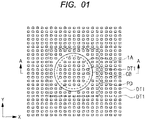
- FIG. 1 shows a rectangular pad (electrode pad) PD shown by a broken line.
- the circle shown in the central of the pad PD is a contour of the outermost periphery of the Cu ball CB configuring the tip of the Cu wire, which is a bonding wire, connected to the upper surface of the pad PD.
- the dotted circle shown on the inside of the circle is a contour of the bottom surface of the Cu ball CB.
- Each of the plurality of squares arranged in a matrix in the X and Y directions in FIG. 1 is a trench isolation DT1 having a rectangular circular layout in plan view.
- the X and Y directions shown in FIG. 1 are the directions along the upper surface (main surface) of the semiconductor substrate.
- the X and Y directions are perpendicular to each other in plan view.
- the direction along each of the X direction and Y direction is referred to as the lateral direction
- the direction perpendicular to each of the X direction and Y direction is referred to as the vertical direction.
- the trench isolation DT1 is an element isolation (element isolation region) including a dielectric film embedded in a trench formed in the upper surface of the semiconductor substrate and a void existed in the dielectric film. That is, each of the sides of the square is a trench, the region inside the square in plan view is a region outside the trench.
- the diameter of the Cu ball CB in plan view is larger than the diameter of the bonding wire.
- FIG. 2 shows a cross-sectional view in line A-A of FIG. 1 .
- the semiconductor device according to the present embodiment has a semiconductor substrate and a trench isolation TI formed of a dielectric film IF1 fully embedded in the first trench D1 in the upper surface of the semiconductor substrate SB.
- the semiconductor substrate SB is made of, for example, single crystal Si (silicon).
- the semiconductor chip has a plurality of trench isolations DT1 formed directly under the trench isolation TI.
- the trench isolation DT1 is formed directly under the trench isolation TI and formed of a second trench D2 deeper than the trench D1, a dielectric film IF1 embedded in the trench D2, and a void (air gap) V1 formed in the dielectric film IF1 in the trench D2.
- the trench D2 is formed in the bottom surface of the trench D1 and extends downward (the back side of the semiconductor substrate SB).
- the trench isolation TI is an element isolation region made of a dielectric film IF1 and formed by, for example, STI (Shallow Trench Isolation) method or LOCOS (LOCal Oxidization of Silicon) method in the main surface of the semiconductor substrate SB.
- the trench isolation DT1 has a DTI (Deep Trench Isolation) structure.
- the trench isolations DT1 are referred to as trench isolations as isolating the element by the trenches, the trench isolations DT1 are dummy element isolations which are not actually used for isolating the element.
- the dummy element isolation is a pseudo element isolation that is provided to suppress manufacturing variations of the trenches D2 formed in the semiconductor chip, including the trenches D2 in which the element isolation contributing to the isolation of the element is formed. That is, the trench isolations DT1 which are dummy element isolations are provided to make the etching depth of the trenches D2 deeper than the trench D1 uniform. By adjusting the occupancy of the trench isolation pattern by placing the dummy element isolations, it is possible to make the etching depth uniform.
- the trench isolation TI in the vicinity of the upper ends of the trench isolations DT1 which are dummy element isolations is also a dummy element isolation.
- An interlayer dielectric film IL is formed on the trench isolation TI, trench isolations DT1 and the semiconductor substrate SB.
- the interlayer dielectric film IL is mainly formed of a silicon oxide film or the like.
- the interlayer dielectric film IL is a laminated wiring layer, and has a structure in which a plurality of wiring layers including wirings made of metal is laminated.
- the semiconductor elements are formed in the vicinity of the upper surface of the semiconductor substrate SB under the interlayer dielectric film IL.
- a pad PD mainly made of Al (aluminum) is formed, for example, on the interlayer dielectric film IL.
- the pad PD is electrically connected to the semiconductor elements via the wirings.
- the upper surface and side surface of the end portion of the pad PD are covered with a passivation film PF covering the upper surface of the interlayer dielectric film IL.
- Cu wire CW which is a bonding wire made of Cu (copper) is connected to the upper surface of the pad PD exposed from the passivation film PF. Specifically, Cu ball CB of the tip of the Cu wire CW is pressed against the upper surface of the pad PD, Cu ball CB is in a state of being collapsed. As a result, a part of the upper surface of the pad PD is raised in the region adjacent to the Cu ball CB.
- the collapsed Cu ball CB is provided with a flat bottom surface and a side surface formed of curved surface.
- FIG. 3 is an enlarged cross-sectional view of a part of FIG. 2 (where indicated by a broken line).
- the semiconductor device according to the present embodiment has a trench isolation arrangement prohibition region 1A.
- the trench isolation arrangement prohibition region 1A is the region between the circle of the broken line and the circle of the solid line shown in FIG. 1 . That is, the trench isolation arrangement prohibition region 1A is a circular region overlapping the end portion of the Cu ball CB in plan view.
- the trench isolation arrangement prohibition region 1A is a region between, of the bottom surface of the Cu ball CB shown in FIG. 3 , the end portion of the bottom surface of the Cu ball CB closest from the void V1 configuring the trench isolation DT1 in the vertical direction and the outermost periphery of the Cu ball CB in the lateral direction and includes a region directly under the Cu ball CB.
- the trench isolation arrangement prohibition region 1A is a shortest region between, of the bottom surface of the Cu ball CB, the end portion of the bottom surface of the Cu ball CB closest from the void V1 configuring the trench isolation DT1 in the vertical direction and the outermost periphery of the Cu ball CB in the radial direction of the Cu ball CB in plan view.
- the main feature of the semiconductor device according to the present embodiment is that the trench isolations DT1 are not disposed in the semiconductor substrate SB in the trench isolation arrangement prohibition region 1A, but are disposed in the semiconductor substrate SB in other than the trench isolation arrangement prohibition region 1A.
- the end portion of the bottom surface of the Cu ball CB closest from the void V1 configuring the trench isolation DT1 in the vertical direction is referred to the end portion of the region in which the distance L is the shortest in the vertical direction (height direction, thickness direction), of the bottom surface of the Cu ball CB shown in FIG. 3 .
- the end portion is a boundary between the region (flat bottom surface) of the bottom surface of the Cu ball CB in which the distance L from the void V1 is the shortest in the vertical direction and the region (side surface having a curved surface) in which the distance from the void V1 to the Cu ball CB in the vertical direction gradually increases toward the outermost periphery of the Cu ball CB.
- the trench isolations DT1 are formed directly under the end portion of the Cu ball CB, that is, in the trench isolation arrangement prohibition region 1A described above, shear stress acts in the semiconductor substrate SB with reference to the trench isolations DT1. Therefore, in the present embodiment, as shown in FIG. 3 , the trench isolations DT1 are not disposed in the trench isolation arrangement prohibition region 1A, thereby preventing the occurrence of the shear stress. Therefore, since silicon peeling, the oxide film peeling, or the occurrence of cracking in the oxide film in the semiconductor chip can be prevented, it is possible to improve the reliability of the semiconductor device. Therefore, the above-mentioned room for improvement can be solved.
- a trench isolation arrangement prohibition region 1B which further expanded the trench isolation arrangement prohibition region 1A in the lateral direction (radial direction of the Cu ball CB in plan view).
- the material of the film embedded in the trench D2 may be made of a polysilicon film or a metal film made of W (tungsten) or the like.
- a conductive film such as a polysilicon film or a metal film is embedded in the trench D2
- a case that a potential is supplied to the semiconductor substrate SB via the conductive film, a case that the conductive film is used for element isolation, or a case that the conductive film is used as a capacitive element, etc. are considered.
- a void V1 is formed in the polysilicon films or the metal films in the trenches D2.
- trench isolations DT2 for electrically isolating the semiconductor elements may be provided.
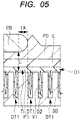
- FIG. 5 is, similarly to FIG. 3 , an enlarged cross-sectional view showing the vicinity of the end portion of the Cu ball CB.
- FIG. 4 in the present embodiment, there is an element region 1C in which the semiconductor elements are formed.
- Trench isolations DT2 having the same structures as the trench isolations DT1 are formed in the semiconductor substrate around the element region 1C.
- the trench isolation DT2 has a rectangular circular structure so as to surround the element region 1C in plan view.
- the element region 1C and the trench isolation DT2 therearound are formed on the inner and outer sides of the trench isolation arrangement prohibition region 1A, respectively, in plan view.
- the trench isolation arrangement prohibition region 1A and the trench isolations DT2 are separated from each other and do not overlap with each other.
- both the trench isolations DT1 which are dummy element isolations and the trench isolations DT2 which are used for the electrical isolation of the element are formed at positions separated from the trench isolation arrangement prohibition region 1A. This prevents shear stress from acting in the semiconductor substrate SB with reference to the trench isolations DT1 or DT2 when the Cu wire is pushed toward the semiconductor substrate SB side or pulled upward. Therefore, since silicon peeling, the oxide film peeling or the occurrence of cracking in the oxide film in the semiconductor chip can be prevented, it is possible to improve the reliability of the semiconductor device.
- the element region 1C may overlap the entire trench isolation arrangement prohibition region 1A in plan view.
- the element region 1C includes entire of the region directly under the Cu ball CB, and in plan view, the trench isolations DT2 surrounding the element region 1C surround the entire trench isolation arrangement prohibition region 1A. That is, the trench isolations DT2 are separated from the trench isolation arrangement prohibition region 1A. Further, in the element region 1C, the trench isolations DT1 are not formed.
- both the trench isolations DT1 which are dummy element isolations and the trench isolations DT2 which are used for electrically isolating the elements are formed at positions separated from the trench isolation arrangement prohibition region 1A. This prevents shear stress from acting in the semiconductor substrate SB with reference to the trench isolations DT1 or DT2 when the Cu wire is pushed toward the semiconductor substrate SB side or pulled upward. Therefore, since silicon peeling, the oxide film peeling or the occurrence of cracking in the oxide film in the semiconductor chip can be prevented, it is possible to improve the reliability of the semiconductor device.
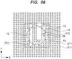
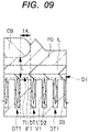
- the element region 1C may overlap a part of the trench isolation arrangement prohibition region 1A in plan view.
- a part of each of the element region 1C and the trench isolations DT2 therearound overlaps the Cu ball CB in plan view.
- the trench isolations DT2 including the void V1 therein are formed in the trench isolation arrangement prohibition region 1A.
- the circular trench isolation arrangement prohibition region 1A and the trench isolations DT2 intersect in plan view, and do not overlap in parallel.
- the trench isolation arrangement prohibition region 1A and the trench isolations DT2 are parallel in plan view, that is, when the trench isolations DT2 extend like the tangent of the circle-shaped trench isolation arrangement prohibition region 1A, shear stress is likely to occur as described in the room for improvement.
- the trench isolation arrangement prohibition region 1A and the trench isolations DT2 intersect in plan view, it is possible to suppress the occurrence of shear stress.
- the angles at which the trench isolation arrangement prohibition region 1A extending in a circular shape and the trench isolations DT2 intersect each other in plan view are preferably, for example, 45 degrees or more and 90 degrees or less.
- the trench isolations DT1 which are dummy element isolations, are separated from the trench isolation arrangement prohibition region 1A. Therefore, in the present modified example, when the Cu wire is pushed to the semiconductor substrate SB side or pulled upward, with reference to the trench isolations DT1 or DT2, it is possible to prevent the shear stress from acting in the semiconductor substrate SB. Therefore, since silicon peeling, the oxide film peeling or the occurrence of cracking in the oxide film in the semiconductor chip can be prevented, it is possible to improve the reliability of the semiconductor device.
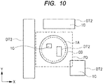
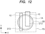
- FIGS. 10 to 12 are planar layouts showing separate embodiment, respectively.
- the structure shown in FIG. 10 does not have trench isolations DT1 which are dummy element isolations.
- each of the element region 1C and trench isolations DT2 therearound are separated from the trench isolation arrangement prohibition region 1A and are located inside or outside the trench isolation arrangement prohibition region 1A in plan view. Since the trench isolations DT2 are not formed in the trench isolation arrangement prohibition region 1A and the trench isolations DT1 that are the dummy element isolations are not formed, the occurrence of shear stress can be more effectively prevented as compared with the second embodiment (see FIG. 4 ).
- the structure shown in FIG. 11 does not have trench isolations DT1 which are dummy element isolations.
- the element region 1C overlaps the entire trench isolation arrangement prohibition region 1A in plan view, and the trench isolations DT2 around the element region 1C are separated from the trench isolation arrangement prohibition region 1A.
- the trench isolations DT2 are not formed in the trench isolation arrangement prohibition region 1A, and since the trench isolations DT1 which are dummy element isolations are not formed, as compared with the first modified example of the second embodiment (see FIG. 6 ), the occurrence of shear stress can be more effectively prevented.
- the structure shown in FIG. 12 does not have trench isolations DT1 which are dummy element isolations.
- the circular trench isolation arrangement prohibition region 1A and the trench isolations DT2 intersect in plan view, and do not overlap in parallel.
- the trench isolations DT1 which are dummy element isolations are not formed. Therefore, compared to the second modified example of the second embodiment (see FIG. 8 ), the occurrence of shear stress can be more effectively prevented.
Landscapes
- Element Separation (AREA)
- Internal Circuitry In Semiconductor Integrated Circuit Devices (AREA)
- Wire Bonding (AREA)
Abstract

Description
- The disclosure of
Japanese Patent Application No. 2021-115299 filed on July 12, 2021 - The present invention relates to semiconductor device, for example, it relates to a technique that is valid by applying to the semiconductor device provided with a trench having a void therein.
- There is a semiconductor device having an element isolation structure in which a dielectric film is formed in a trench formed on a surface as a main surface of a semiconductor substrate. Further, there is a semiconductor device having an element isolation (DTI: Deep Trench Isolation) structure (trench isolation) in which a dielectric film having a void is formed in a trench having a high aspect ratio higher than 1 as the aspect ratio that is the ratio of the depth of the trench to the width of the trench. When connecting the semiconductor chip and the lead frame or the like, it is known to connect the Cu wire (bonding wire) with a Cu ball at the tip to the pad on the surface of the semiconductor chip.
- There are disclosed techniques listed below.
[Patent Document 1]Japanese Unexamined Patent Application Publication No. 2008-135692 -
Patent Document 1 discloses the problem that the Cu electrode is swung by vibration at the time of bonding and cracking occurs in the interlayer dielectric film under the Cu electrode. Here, it is described that the uppermost wiring and electrode layer disposed in the lower layer of the pad portion is formed of a material having a Young's modulus larger than that of the pad portion, thereby preventing the electrode from swinging during bonding. - In the semiconductor chip having a trench isolation having a void therein, when performing a push-pull test for connection strength evaluation of the Cu wire, shear stress acts on the boundary of the void of the trench isolation directly under the outer peripheral portion of the Cu ball, there is a problem Si peeling or cracking is likely to occur.
- Other objects and novel features will become apparent from the description of this specification and the accompanying drawings.
- The typical ones of the embodiments disclosed in the present application will be briefly described as follows.
- A semiconductor device according to one embodiment has a first trench isolation in a first trench formed in an upper surface of a semiconductor substrate, a second trench isolation having a void directly under the first trench isolation, and a bonding wire having a ball and connected to a pad on the semiconductor substrate. The semiconductor device has a circular trench isolation arrangement prohibition region that overlaps with the end portion of the ball in plan view and the second trench isolation is separated from the trench isolation arrangement prohibition region in plan view.
- According to one embodiment, the reliability of the semiconductor device can be improved.
-
-
FIG. 1 is a planar layout showing a semiconductor device according to first embodiment. -
FIG. 2 is a cross-sectional view in line A-A ofFIG. 1 . -
FIG. 3 is an enlarged cross-sectional view of a portion ofFIG. 2 . -
FIG. 4 is a planar layout showing a semiconductor device according to second embodiment. -
FIG. 5 is an enlarged cross-sectional view showing a semiconductor device according to the second embodiment. -
FIG. 6 is a planar layout showing a semiconductor device according to first modified example of the second embodiment. -
FIG. 7 is an enlarged cross-sectional view showing a semiconductor device according to the first modified example of the second embodiment. -
FIG. 8 is a planar layout showing a semiconductor device according to second modified example of the second embodiment. -
FIG. 9 is an enlarged cross-sectional view showing a semiconductor device according to the second modified example of the second embodiment. -
FIG. 10 is a planar layout showing a semiconductor device according to third embodiment. -
FIG. 11 is a planar layout showing a semiconductor device according to the third embodiment. -
FIG. 12 is a planar layout showing a semiconductor device according to the third embodiment. -
FIG. 13 is a planar layout showing a semiconductor device according to comparative example. -
FIG. 14 is a cross-sectional view showing a semiconductor device according to the comparative example. -
FIG. 15 is a cross-sectional view showing a semiconductor device according to the comparative example. - In the following embodiments, when required for convenience, the description will be made by dividing into a plurality of sections or embodiments, but except when specifically stated, they are not independent of each other, and one is related to the modified example, detail, supplementary description, or the like of part or all of the other. In addition, in the following embodiments, the number of elements or the like (including the number, the number, the amount, the range, and the like) is not limited to the mentioned number, except the case where it is specified in particular or the case where it is obviously limited to a specific number in principle, and may be equal to or more than the mentioned number or may be equal to or less than the mentioned number.
- Furthermore, in the following embodiments, the constituent elements (including element steps and the like) are not necessarily essential except for the case in which they are specifically specified, the case in which they are considered to be obviously essential in principle, and the like. Similarly, in the following embodiments, when referring to the shapes, positional relationships, and the like of components and the like, it is assumed that the shapes and the like are substantially approximate to or similar to the shapes and the like, except for the case in which they are specifically specified and the case in which they are considered to be obvious in principle, and the like. The same applies to the above numerical values and ranges.
- Hereinafter, embodiments will be described in detail with reference to the drawings. In all the drawings for explaining the embodiments, members having the same functions are denoted by the same reference numerals, and repetitive descriptions thereof are omitted. In the following embodiments, descriptions of the same or similar parts will not be repeated in principle except when particularly necessary.
-
FIG. 13 shows a planar layout of a semiconductor chip which is a semiconductor device according to comparative example.FIG. 13 shows a rectangular pad (electrode pad) PD indicated by a broken line. The circle shown in the central of the pad PD is the contour of the outermost periphery of the Cu ball CB at the tip of the Cu wire which is a bonding wire connected to an upper surface of the pad PD. The dotted circle shown on the inside of the circle is a contour of the bottom surface of the Cu ball CB. Each of the plurality of squares arranged on the matrix inFIG. 13 is a trench isolation DT1 having a rectangular circular layout in plan view. The trench isolation DT1 is an element isolation (element isolation region) including a dielectric film embedded in a trench formed in an upper surface of a semiconductor substrate and a void existed in the dielectric film. That is, each of sides of the square is a trench, the region inside the square in plan view is a region outside the trench. - In the comparative example, the trench isolation DT1 is disposed without any restrictions on the arrangement, including directly under the pad PD. Therefore, the trench isolation DT1 is disposed directly under the region between the end portion of the bottom surface of the Cu ball CB shown by a broken line circle in
FIG. 15 and the outermost periphery of the Cu ball CB shown by a solid circle. -
FIGS. 14 and15 show enlarged cross-sectional views including the region near the end portion of the Cu ball CB and directly under the Cu ball CB. As shown inFIGS. 14 and15 , the semiconductor chip that is a semiconductor device according to the comparative example has a semiconductor substrate SB, and a trench isolation TI formed of a dielectric film IF1 embedded in the first trench D1 in an upper surface of the semiconductor substrate SB. Further, the semiconductor chip has a plurality of trench isolation DT1 formed directly under the trench isolation TI. The trench isolation DT1 is formed directly under the trench isolation TI and formed of a second trench D2 deeper than the trench D1, a dielectric film IF1 embedded in the trench D2, and a void V1 formed in the dielectric film IF1 in the trench D2. - Here, in the semiconductor device in which the Cu wire is connected to the pad PD on the upper surface of the semiconductor chip, after connecting the Cu wire, a push-pull test for evaluating the connection strength of the Cu wire. In the push-pull test, a test for pressing the Cu wire to the semiconductor chip side, and a test for pulling the Cu wire in a direction away from the semiconductor chip.
- At this time, when pressing the Cu wire to the semiconductor chip side, with reference to the trench isolation DT1 directly under the end portion of the Cu ball CB, in the Cu ball CB side, the force is applied in the direction of pressing the semiconductor substrate SB, in the outside of the Cu ball CB, the force acts in the direction of pushing up the semiconductor substrate SB. Conversely, when pulling the Cu wire upward, with reference to the trench isolation DT1 directly under the end portion of the Cu ball CB, the force is applied to pull up the semiconductor substrate SB in the Cu ball CB side, and in the outside of the Cu ball CB, force is applied in the direction to push down the semiconductor substrate SB. Therefore, the shear stress acts on the boundary of the void V1 of the trench isolation DT1 through the push-pull test, silicon peeling (peeling of the silicon substrate), the oxide film peeling, or cracking in the oxide film is likely to occur. The cracking or the like occurs at a place indicated by a thick broken line in
FIGS. 14 and15 with the void V1 at the lower end of the broken line as a starting point. - Thus, in the semiconductor device having a trench isolation with a void V1 and in which wire bonding is performed, there is room for improving the reliability of the semiconductor device by preventing the silicon peeling or cracking when a force is applied to the Cu wire.
- The structure of the semiconductor device according to the present embodiment is described below with reference to
FIGs. 1 to 3 . The semiconductor device is a semiconductor chip, and the semiconductor chip is provided with a semiconductor element such as a MISFET (Metal Insulator Semiconductor Field Effect Transistor), a diode, a resistive element or a capacitive element. These semiconductor elements are formed in an upper surface vicinity of the semiconductor substrate or in the semiconductor substrate configuring the semiconductor chip. -
FIG. 1 shows a rectangular pad (electrode pad) PD shown by a broken line. The circle shown in the central of the pad PD is a contour of the outermost periphery of the Cu ball CB configuring the tip of the Cu wire, which is a bonding wire, connected to the upper surface of the pad PD. The dotted circle shown on the inside of the circle is a contour of the bottom surface of the Cu ball CB. Each of the plurality of squares arranged in a matrix in the X and Y directions inFIG. 1 is a trench isolation DT1 having a rectangular circular layout in plan view. The X and Y directions shown inFIG. 1 are the directions along the upper surface (main surface) of the semiconductor substrate. The X and Y directions are perpendicular to each other in plan view. In the present application, the direction along each of the X direction and Y direction is referred to as the lateral direction, the direction perpendicular to each of the X direction and Y direction is referred to as the vertical direction. The trench isolation DT1 is an element isolation (element isolation region) including a dielectric film embedded in a trench formed in the upper surface of the semiconductor substrate and a void existed in the dielectric film. That is, each of the sides of the square is a trench, the region inside the square in plan view is a region outside the trench. The diameter of the Cu ball CB in plan view is larger than the diameter of the bonding wire. -
FIG. 2 shows a cross-sectional view in line A-A ofFIG. 1 . As shown inFIG. 2 , the semiconductor device according to the present embodiment has a semiconductor substrate and a trench isolation TI formed of a dielectric film IF1 fully embedded in the first trench D1 in the upper surface of the semiconductor substrate SB. The semiconductor substrate SB is made of, for example, single crystal Si (silicon). Further, the semiconductor chip has a plurality of trench isolations DT1 formed directly under the trench isolation TI. The trench isolation DT1 is formed directly under the trench isolation TI and formed of a second trench D2 deeper than the trench D1, a dielectric film IF1 embedded in the trench D2, and a void (air gap) V1 formed in the dielectric film IF1 in the trench D2. The trench D2 is formed in the bottom surface of the trench D1 and extends downward (the back side of the semiconductor substrate SB). - The trench isolation TI is an element isolation region made of a dielectric film IF1 and formed by, for example, STI (Shallow Trench Isolation) method or LOCOS (LOCal Oxidization of Silicon) method in the main surface of the semiconductor substrate SB. The trench isolation DT1 has a DTI (Deep Trench Isolation) structure. Here, the trench isolations DT1 are referred to as trench isolations as isolating the element by the trenches, the trench isolations DT1 are dummy element isolations which are not actually used for isolating the element. The dummy element isolation is a pseudo element isolation that is provided to suppress manufacturing variations of the trenches D2 formed in the semiconductor chip, including the trenches D2 in which the element isolation contributing to the isolation of the element is formed. That is, the trench isolations DT1 which are dummy element isolations are provided to make the etching depth of the trenches D2 deeper than the trench D1 uniform. By adjusting the occupancy of the trench isolation pattern by placing the dummy element isolations, it is possible to make the etching depth uniform. The trench isolation TI in the vicinity of the upper ends of the trench isolations DT1 which are dummy element isolations is also a dummy element isolation.
- An interlayer dielectric film IL is formed on the trench isolation TI, trench isolations DT1 and the semiconductor substrate SB. The interlayer dielectric film IL is mainly formed of a silicon oxide film or the like. However, in practice, the interlayer dielectric film IL is a laminated wiring layer, and has a structure in which a plurality of wiring layers including wirings made of metal is laminated. Although not shown in
FIG. 2 , the semiconductor elements are formed in the vicinity of the upper surface of the semiconductor substrate SB under the interlayer dielectric film IL. A pad PD mainly made of Al (aluminum) is formed, for example, on the interlayer dielectric film IL. The pad PD is electrically connected to the semiconductor elements via the wirings. The upper surface and side surface of the end portion of the pad PD are covered with a passivation film PF covering the upper surface of the interlayer dielectric film IL. - Cu wire CW which is a bonding wire made of Cu (copper) is connected to the upper surface of the pad PD exposed from the passivation film PF. Specifically, Cu ball CB of the tip of the Cu wire CW is pressed against the upper surface of the pad PD, Cu ball CB is in a state of being collapsed. As a result, a part of the upper surface of the pad PD is raised in the region adjacent to the Cu ball CB. The collapsed Cu ball CB is provided with a flat bottom surface and a side surface formed of curved surface.
- The main features of the semiconductor device according to the present embodiment will be described with reference to
FIGS. 1 and3. FIG. 3 is an enlarged cross-sectional view of a part ofFIG. 2 (where indicated by a broken line). As shown inFIG. 3 , the semiconductor device according to the present embodiment has a trench isolationarrangement prohibition region 1A. The trench isolationarrangement prohibition region 1A is the region between the circle of the broken line and the circle of the solid line shown inFIG. 1 . That is, the trench isolationarrangement prohibition region 1A is a circular region overlapping the end portion of the Cu ball CB in plan view. - Specifically, the trench isolation
arrangement prohibition region 1A is a region between, of the bottom surface of the Cu ball CB shown inFIG. 3 , the end portion of the bottom surface of the Cu ball CB closest from the void V1 configuring the trench isolation DT1 in the vertical direction and the outermost periphery of the Cu ball CB in the lateral direction and includes a region directly under the Cu ball CB. In other words, the trench isolationarrangement prohibition region 1A is a shortest region between, of the bottom surface of the Cu ball CB, the end portion of the bottom surface of the Cu ball CB closest from the void V1 configuring the trench isolation DT1 in the vertical direction and the outermost periphery of the Cu ball CB in the radial direction of the Cu ball CB in plan view. The main feature of the semiconductor device according to the present embodiment is that the trench isolations DT1 are not disposed in the semiconductor substrate SB in the trench isolationarrangement prohibition region 1A, but are disposed in the semiconductor substrate SB in other than the trench isolationarrangement prohibition region 1A. - The end portion of the bottom surface of the Cu ball CB closest from the void V1 configuring the trench isolation DT1 in the vertical direction is referred to the end portion of the region in which the distance L is the shortest in the vertical direction (height direction, thickness direction), of the bottom surface of the Cu ball CB shown in
FIG. 3 . The end portion is a boundary between the region (flat bottom surface) of the bottom surface of the Cu ball CB in which the distance L from the void V1 is the shortest in the vertical direction and the region (side surface having a curved surface) in which the distance from the void V1 to the Cu ball CB in the vertical direction gradually increases toward the outermost periphery of the Cu ball CB. - As described with reference to
FIGS. 14 and15 , when the Cu wire is pushed toward the semiconductor substrate SB or pulled upward, if the trench isolations DT1 are formed directly under the end portion of the Cu ball CB, that is, in the trench isolationarrangement prohibition region 1A described above, shear stress acts in the semiconductor substrate SB with reference to the trench isolations DT1. Therefore, in the present embodiment, as shown inFIG. 3 , the trench isolations DT1 are not disposed in the trench isolationarrangement prohibition region 1A, thereby preventing the occurrence of the shear stress. Therefore, since silicon peeling, the oxide film peeling, or the occurrence of cracking in the oxide film in the semiconductor chip can be prevented, it is possible to improve the reliability of the semiconductor device. Therefore, the above-mentioned room for improvement can be solved. - Further, in order to prevent silicon peeling, the oxide film peeling, or the occurrence of cracking more reliably in the oxide film, it is necessary to consider misalignment of the Cu ball CB and diameter variation of the Cu ball CB. Therefore, it is more preferable to provide a trench isolation
arrangement prohibition region 1B which further expanded the trench isolationarrangement prohibition region 1A in the lateral direction (radial direction of the Cu ball CB in plan view). - Although it is explained that the dielectric film IF1 with the void V1 is buried in the trench D2, the material of the film embedded in the trench D2 may be made of a polysilicon film or a metal film made of W (tungsten) or the like. As a case that a conductive film such as a polysilicon film or a metal film is embedded in the trench D2, a case that a potential is supplied to the semiconductor substrate SB via the conductive film, a case that the conductive film is used for element isolation, or a case that the conductive film is used as a capacitive element, etc. are considered. Whether the polysilicon films or the metal films are embedded in the trenches D2, a void V1 is formed in the polysilicon films or the metal films in the trenches D2. By not forming the trench isolations including such films in the trench isolation
arrangement prohibition region 1A, the above-described effects according to the present embodiment can be obtained. - As shown in
FIGS. 4 and5 (in particular,FIG. 4 ), trench isolations DT2 for electrically isolating the semiconductor elements may be provided.FIG. 5 is, similarly toFIG. 3 , an enlarged cross-sectional view showing the vicinity of the end portion of the Cu ball CB. As shown inFIG. 4 , in the present embodiment, there is anelement region 1C in which the semiconductor elements are formed. Trench isolations DT2 having the same structures as the trench isolations DT1 are formed in the semiconductor substrate around theelement region 1C. The trench isolation DT2 has a rectangular circular structure so as to surround theelement region 1C in plan view. - Here, the
element region 1C and the trench isolation DT2 therearound are formed on the inner and outer sides of the trench isolationarrangement prohibition region 1A, respectively, in plan view. However, in plan view, the trench isolationarrangement prohibition region 1A and the trench isolations DT2 are separated from each other and do not overlap with each other. - In the present embodiment, both the trench isolations DT1 which are dummy element isolations and the trench isolations DT2 which are used for the electrical isolation of the element, are formed at positions separated from the trench isolation
arrangement prohibition region 1A. This prevents shear stress from acting in the semiconductor substrate SB with reference to the trench isolations DT1 or DT2 when the Cu wire is pushed toward the semiconductor substrate SB side or pulled upward. Therefore, since silicon peeling, the oxide film peeling or the occurrence of cracking in the oxide film in the semiconductor chip can be prevented, it is possible to improve the reliability of the semiconductor device. - As shown in
FIGS. 6 and7 , theelement region 1C may overlap the entire trench isolationarrangement prohibition region 1A in plan view. In this case, theelement region 1C includes entire of the region directly under the Cu ball CB, and in plan view, the trench isolations DT2 surrounding theelement region 1C surround the entire trench isolationarrangement prohibition region 1A. That is, the trench isolations DT2 are separated from the trench isolationarrangement prohibition region 1A. Further, in theelement region 1C, the trench isolations DT1 are not formed. - In the present modified example, both the trench isolations DT1 which are dummy element isolations and the trench isolations DT2 which are used for electrically isolating the elements, are formed at positions separated from the trench isolation
arrangement prohibition region 1A. This prevents shear stress from acting in the semiconductor substrate SB with reference to the trench isolations DT1 or DT2 when the Cu wire is pushed toward the semiconductor substrate SB side or pulled upward. Therefore, since silicon peeling, the oxide film peeling or the occurrence of cracking in the oxide film in the semiconductor chip can be prevented, it is possible to improve the reliability of the semiconductor device. - As shown in
FIGS. 8 and9 , theelement region 1C may overlap a part of the trench isolationarrangement prohibition region 1A in plan view. Here, a part of each of theelement region 1C and the trench isolations DT2 therearound overlaps the Cu ball CB in plan view. Here, the trench isolations DT2 including the void V1 therein are formed in the trench isolationarrangement prohibition region 1A. However, the circular trench isolationarrangement prohibition region 1A and the trench isolations DT2 intersect in plan view, and do not overlap in parallel. - When the trench isolation
arrangement prohibition region 1A and the trench isolations DT2 are parallel in plan view, that is, when the trench isolations DT2 extend like the tangent of the circle-shaped trench isolationarrangement prohibition region 1A, shear stress is likely to occur as described in the room for improvement. However, as in the present modified example, when the trench isolationarrangement prohibition region 1A and the trench isolations DT2 intersect in plan view, it is possible to suppress the occurrence of shear stress. The angles at which the trench isolationarrangement prohibition region 1A extending in a circular shape and the trench isolations DT2 intersect each other in plan view are preferably, for example, 45 degrees or more and 90 degrees or less. - In the present modified example, similar to the above-mentioned first embodiment, the trench isolations DT1 which are dummy element isolations, are separated from the trench isolation
arrangement prohibition region 1A. Therefore, in the present modified example, when the Cu wire is pushed to the semiconductor substrate SB side or pulled upward, with reference to the trench isolations DT1 or DT2, it is possible to prevent the shear stress from acting in the semiconductor substrate SB. Therefore, since silicon peeling, the oxide film peeling or the occurrence of cracking in the oxide film in the semiconductor chip can be prevented, it is possible to improve the reliability of the semiconductor device. - In the first embodiment and the second embodiment, the case where trench isolations which are dummy element isolations are formed has been described, but hereinafter, the case where there is no dummy element isolations will be described with reference to
FIGS. 10 to 12 .FIGs 10 ,11 and12 are planar layouts showing separate embodiment, respectively. - Unlike the structure described with reference to
FIG. 4 , the structure shown inFIG. 10 does not have trench isolations DT1 which are dummy element isolations. Here, each of theelement region 1C and trench isolations DT2 therearound are separated from the trench isolationarrangement prohibition region 1A and are located inside or outside the trench isolationarrangement prohibition region 1A in plan view. Since the trench isolations DT2 are not formed in the trench isolationarrangement prohibition region 1A and the trench isolations DT1 that are the dummy element isolations are not formed, the occurrence of shear stress can be more effectively prevented as compared with the second embodiment (seeFIG. 4 ). - Unlike the structure described with reference to
FIG. 6 , the structure shown inFIG. 11 does not have trench isolations DT1 which are dummy element isolations. Here, theelement region 1C overlaps the entire trench isolationarrangement prohibition region 1A in plan view, and the trench isolations DT2 around theelement region 1C are separated from the trench isolationarrangement prohibition region 1A. Thus, the trench isolations DT2 are not formed in the trench isolationarrangement prohibition region 1A, and since the trench isolations DT1 which are dummy element isolations are not formed, as compared with the first modified example of the second embodiment (seeFIG. 6 ), the occurrence of shear stress can be more effectively prevented. - Unlike the structure described with reference to
FIG. 8 , the structure shown inFIG. 12 does not have trench isolations DT1 which are dummy element isolations. Here, a part of each of theelement region 1C and the trench isolations DT2 therearound overlap the trench isolationarrangement prohibition region 1A in plan view. However, the circular trench isolationarrangement prohibition region 1A and the trench isolations DT2 intersect in plan view, and do not overlap in parallel. Further, the trench isolations DT1 which are dummy element isolations are not formed. Therefore, compared to the second modified example of the second embodiment (seeFIG. 8 ), the occurrence of shear stress can be more effectively prevented. - Although the invention made by the present inventor has been specifically described based on the embodiment, the present invention is not limited to the as described above embodiment, and it is needless to say that various modifications can be made without departing from the gist thereof.
Claims (10)
- A semiconductor device, comprising:a semiconductor substrate;a first trench formed on the semiconductor substrate;a second trench formed in a bottom surface of the first trench and having a deeper depth than the first trench;a first trench isolation formed of a first film embedded in the first trench;a second trench isolation formed of a second film, the second film being embedded in the second trench and having a first void therein in the second trench;a bonding wire connected to an upper surface of a pad on the first trench isolation, the second trench isolation and the semiconductor substrate;a ball configuring a tip of the bonding wire; anda circular first region overlapped with an end portion of the ball in plan view,wherein the first region is a region between an end portion of a bottom surface of the ball closest from the first void in a first direction perpendicular to an upper surface of the semiconductor substrate and an outermost periphery of the ball in a second direction along the upper surface of the semiconductor substrate, and includes directly under the ball, andwherein the second trench isolation is separated from the first region in plan view.
- The semiconductor device according to claim 1, comprising:a third trench formed in the bottom surface of the first trench and having a deeper depth than the first trench;a third trench isolation formed of the second film, the second film being embedded in the third trench and having a second void therein in the third trench; andan element region in which a semiconductor element is formed,wherein the third trench isolation electrically isolate the semiconductor element,wherein the second trench isolation is a pseudo element isolation, andwherein the third trench isolation is separated from the first region in plan view.
- The semiconductor device according to claim 1 or 2,
wherein, in plan view, the element region overlaps with an entire of the ball, and the third trench isolation surrounds the first region. - The semiconductor device according to any one of claims 1 to 3, comprising:a third trench formed in the bottom surface of the first trench and having a deeper depth than the first trench;a third trench isolation formed of the second film, the second film being embedded in the third trench and having a second void therein in the third trench; andan element region in which a semiconductor element is formed,wherein the third trench isolation electrically isolate the semiconductor element,wherein the second trench isolation is a pseudo element isolation, andwherein the third trench isolation intersects the first region in plan view.
- The semiconductor device according to any one of claims 1 to 4,
wherein the second film is a dielectric film, a silicon film or a metal film. - The semiconductor device according to any one of claims 1 to 5,
wherein the second trench isolation is a pseudo element isolation. - The semiconductor device according to any one of claims 1 to 6, comprising:an element region in which a semiconductor element is formed, andwherein the second trench isolation electrically isolate the semiconductor element.
- The semiconductor device according to claim 7,
wherein, in plan view, the element region overlaps with an entire of the ball, and the second trench isolation surrounds the first region. - A semiconductor device, comprising:a semiconductor substrate;a first trench formed on the semiconductor substrate;a second trench formed in a bottom surface of the first trench and having a deeper depth than the first trench;a first trench isolation formed of a first film embedded in the first trench;a second trench isolation formed of a second film, the second film being embedded in the second trench and having a first void therein in the second trench;a bonding wire connected to an upper surface of a pad on the first trench isolation, the second trench isolation and the semiconductor substrate;a ball configuring a tip of the bonding wire;a circular first region overlapped with an end portion of the ball in plan view; andan element region in which a semiconductor element is formed,wherein the second trench isolation electrically isolate the semiconductor element,wherein the first region is a region between an end portion of a bottom surface of the ball closest from the first void in a first direction perpendicular to an upper surface of the semiconductor substrate and an outermost periphery of the ball in a second direction along the upper surface of the semiconductor substrate, and includes directly under the ball, andwherein the second trench isolation intersects the first region in plan view.
- The semiconductor device according to claim 9,
wherein the second film is a dielectric film, a silicon film or a metal film.
Applications Claiming Priority (1)
| Application Number | Priority Date | Filing Date | Title |
|---|---|---|---|
| JP2021115299A JP7577623B2 (en) | 2021-07-12 | 2021-07-12 | Semiconductor Device |
Publications (2)
| Publication Number | Publication Date |
|---|---|
| EP4120340A2 true EP4120340A2 (en) | 2023-01-18 |
| EP4120340A3 EP4120340A3 (en) | 2023-06-07 |
Family
ID=82838963
Family Applications (1)
| Application Number | Title | Priority Date | Filing Date |
|---|---|---|---|
| EP22184003.6A Pending EP4120340A3 (en) | 2021-07-12 | 2022-07-11 | Semiconductor device |
Country Status (4)
| Country | Link |
|---|---|
| US (1) | US12288760B2 (en) |
| EP (1) | EP4120340A3 (en) |
| JP (1) | JP7577623B2 (en) |
| CN (1) | CN115621276A (en) |
Families Citing this family (1)
| Publication number | Priority date | Publication date | Assignee | Title |
|---|---|---|---|---|
| JP2023171042A (en) * | 2022-05-20 | 2023-12-01 | ローム株式会社 | semiconductor equipment |
Citations (2)
| Publication number | Priority date | Publication date | Assignee | Title |
|---|---|---|---|---|
| JP2008135692A (en) | 2006-10-24 | 2008-06-12 | Denso Corp | Semiconductor device |
| US20210225787A1 (en) * | 2018-11-15 | 2021-07-22 | Changxin Memory Technologies, Inc. | Redistribution layer (rdl) structure, semiconductor device and manufacturing method thereof |
Family Cites Families (18)
| Publication number | Priority date | Publication date | Assignee | Title |
|---|---|---|---|---|
| JP3142318B2 (en) * | 1991-08-08 | 2001-03-07 | 新電元工業株式会社 | Semiconductor device |
| JP3582958B2 (en) * | 1996-05-28 | 2004-10-27 | 株式会社東芝 | Semiconductor device and manufacturing method thereof |
| JP2001339071A (en) * | 2000-03-22 | 2001-12-07 | Mitsubishi Electric Corp | Semiconductor device and manufacturing method thereof |
| DE102007050610A1 (en) * | 2006-10-24 | 2008-05-08 | Denso Corp., Kariya | Semiconductor device, wiring of a semiconductor device and method for forming a wiring |
| US20080246152A1 (en) * | 2007-04-04 | 2008-10-09 | Taiwan Semiconductor Manufacturing Co., Ltd. | Semiconductor device with bonding pad |
| CN101821853B (en) * | 2007-11-09 | 2012-06-27 | 三垦电气株式会社 | Semiconductor device and manufacturing method thereof |
| JP5882069B2 (en) * | 2011-03-29 | 2016-03-09 | エスアイアイ・セミコンダクタ株式会社 | Semiconductor device and manufacturing method thereof |
| US9663354B2 (en) * | 2014-05-14 | 2017-05-30 | Infineon Technologies Ag | Mechanical stress-decoupling in semiconductor device |
| JP2017045910A (en) * | 2015-08-28 | 2017-03-02 | ルネサスエレクトロニクス株式会社 | Semiconductor device and manufacturing method of semiconductor device |
| JP6538960B2 (en) * | 2016-02-23 | 2019-07-03 | ルネサスエレクトロニクス株式会社 | Semiconductor device and method of manufacturing the same |
| JPWO2018020713A1 (en) * | 2016-07-28 | 2019-05-09 | パナソニックIpマネジメント株式会社 | Semiconductor device and method of manufacturing the same |
| DE102016116273B4 (en) * | 2016-08-31 | 2024-07-18 | Infineon Technologies Austria Ag | Semiconductor device and method for forming a semiconductor device |
| JP6936027B2 (en) * | 2017-03-09 | 2021-09-15 | ルネサスエレクトロニクス株式会社 | Semiconductor devices and their manufacturing methods |
| JP2019114673A (en) * | 2017-12-25 | 2019-07-11 | ルネサスエレクトロニクス株式会社 | Semiconductor device and method of manufacturing the same |
| JP2019169639A (en) * | 2018-03-23 | 2019-10-03 | ルネサスエレクトロニクス株式会社 | Semiconductor device and manufacturing method thereof |
| US11502036B2 (en) * | 2020-02-07 | 2022-11-15 | Renesas Electronics Corporation | Semiconductor device and method of manufacturing the same |
| JP2021153149A (en) * | 2020-03-24 | 2021-09-30 | キオクシア株式会社 | Semiconductor device |
| KR102833169B1 (en) * | 2020-07-20 | 2025-07-11 | 삼성전자주식회사 | Semiconductor device and method of manufacturing the semiconductor device |
-
2021
- 2021-07-12 JP JP2021115299A patent/JP7577623B2/en active Active
-
2022
- 2022-06-08 US US17/835,541 patent/US12288760B2/en active Active
- 2022-06-23 CN CN202210718640.0A patent/CN115621276A/en active Pending
- 2022-07-11 EP EP22184003.6A patent/EP4120340A3/en active Pending
Patent Citations (2)
| Publication number | Priority date | Publication date | Assignee | Title |
|---|---|---|---|---|
| JP2008135692A (en) | 2006-10-24 | 2008-06-12 | Denso Corp | Semiconductor device |
| US20210225787A1 (en) * | 2018-11-15 | 2021-07-22 | Changxin Memory Technologies, Inc. | Redistribution layer (rdl) structure, semiconductor device and manufacturing method thereof |
Also Published As
| Publication number | Publication date |
|---|---|
| US12288760B2 (en) | 2025-04-29 |
| CN115621276A (en) | 2023-01-17 |
| JP7577623B2 (en) | 2024-11-05 |
| EP4120340A3 (en) | 2023-06-07 |
| JP2023011445A (en) | 2023-01-24 |
| US20230010383A1 (en) | 2023-01-12 |
Similar Documents
| Publication | Publication Date | Title |
|---|---|---|
| KR101360815B1 (en) | Bond pad support structure for semiconductor device | |
| JP5205066B2 (en) | Semiconductor device and manufacturing method thereof | |
| CN101150094B (en) | semiconductor wafer structure | |
| US6537849B1 (en) | Seal ring structure for radio frequency integrated circuits | |
| CN113437077B (en) | Semiconductor devices | |
| EP1783834B1 (en) | Support structure for semiconductor device bond pads and method of making the same | |
| JP2008527710A (en) | Method and apparatus for realizing structure support for wiring pad while increasing signal conduction efficiency | |
| JP2009105160A (en) | Semiconductor device | |
| CN103855157B (en) | MIM capacitor and manufacture method thereof | |
| US6576970B2 (en) | Bonding pad structure of semiconductor device and method for fabricating the same | |
| US7196428B2 (en) | Bond pad structure for integrated circuit chip | |
| US12288760B2 (en) | Semiconductor device | |
| US7531903B2 (en) | Interconnection structure used in a pad region of a semiconductor substrate | |
| EP0431490B1 (en) | Semiconductor integrated circuit device having pads at periphery of semiconductor chip | |
| JP4851163B2 (en) | Manufacturing method of semiconductor device | |
| KR100495288B1 (en) | Semiconductor device and method of manufacturing the same | |
| WO2006046302A1 (en) | Semiconductor device and manufacturing method therefor | |
| US9691714B2 (en) | Semiconductor device and method for manufacturing semiconductor device | |
| US20070123021A1 (en) | Circuit under pad structure and bonding pad process | |
| JP2005327913A (en) | Semiconductor device | |
| KR102845543B1 (en) | Semiconductor device | |
| JP2005005564A (en) | Pad structure | |
| JP2009218503A (en) | Semiconductor device and manufacturing method thereof | |
| JP2013065890A (en) | Semiconductor device and manufacturing method of the same | |
| JP2006019312A (en) | Semiconductor integrated circuit device |
Legal Events
| Date | Code | Title | Description |
|---|---|---|---|
| PUAI | Public reference made under article 153(3) epc to a published international application that has entered the european phase |
Free format text: ORIGINAL CODE: 0009012 |
|
| STAA | Information on the status of an ep patent application or granted ep patent |
Free format text: STATUS: THE APPLICATION HAS BEEN PUBLISHED |
|
| AK | Designated contracting states |
Kind code of ref document: A2 Designated state(s): AL AT BE BG CH CY CZ DE DK EE ES FI FR GB GR HR HU IE IS IT LI LT LU LV MC MK MT NL NO PL PT RO RS SE SI SK SM TR |
|
| PUAL | Search report despatched |
Free format text: ORIGINAL CODE: 0009013 |
|
| AK | Designated contracting states |
Kind code of ref document: A3 Designated state(s): AL AT BE BG CH CY CZ DE DK EE ES FI FR GB GR HR HU IE IS IT LI LT LU LV MC MK MT NL NO PL PT RO RS SE SI SK SM TR |
|
| RIC1 | Information provided on ipc code assigned before grant |
Ipc: H01L 29/06 20060101ALI20230428BHEP Ipc: H01L 21/762 20060101ALI20230428BHEP Ipc: H01L 21/764 20060101ALI20230428BHEP Ipc: H01L 21/308 20060101ALI20230428BHEP Ipc: H01L 23/49 20060101ALI20230428BHEP Ipc: H01L 23/485 20060101AFI20230428BHEP |
|
| STAA | Information on the status of an ep patent application or granted ep patent |
Free format text: STATUS: REQUEST FOR EXAMINATION WAS MADE |
|
| 17P | Request for examination filed |
Effective date: 20231201 |
|
| RBV | Designated contracting states (corrected) |
Designated state(s): AL AT BE BG CH CY CZ DE DK EE ES FI FR GB GR HR HU IE IS IT LI LT LU LV MC MK MT NL NO PL PT RO RS SE SI SK SM TR |
|
| STAA | Information on the status of an ep patent application or granted ep patent |
Free format text: STATUS: EXAMINATION IS IN PROGRESS |
|
| 17Q | First examination report despatched |
Effective date: 20240925 |