EP4120334A2 - Electronic device - Google Patents
Electronic device Download PDFInfo
- Publication number
- EP4120334A2 EP4120334A2 EP22181486.6A EP22181486A EP4120334A2 EP 4120334 A2 EP4120334 A2 EP 4120334A2 EP 22181486 A EP22181486 A EP 22181486A EP 4120334 A2 EP4120334 A2 EP 4120334A2
- Authority
- EP
- European Patent Office
- Prior art keywords
- electronic device
- substrate
- layer
- electronic component
- metal layer
- Prior art date
- Legal status (The legal status is an assumption and is not a legal conclusion. Google has not performed a legal analysis and makes no representation as to the accuracy of the status listed.)
- Pending
Links
Images

Classifications
-
- H—ELECTRICITY
- H10—SEMICONDUCTOR DEVICES; ELECTRIC SOLID-STATE DEVICES NOT OTHERWISE PROVIDED FOR
- H10H—INORGANIC LIGHT-EMITTING SEMICONDUCTOR DEVICES HAVING POTENTIAL BARRIERS
- H10H20/00—Individual inorganic light-emitting semiconductor devices having potential barriers, e.g. light-emitting diodes [LED]
- H10H20/80—Constructional details
- H10H20/85—Packages
- H10H20/852—Encapsulations
-
- H—ELECTRICITY
- H10—SEMICONDUCTOR DEVICES; ELECTRIC SOLID-STATE DEVICES NOT OTHERWISE PROVIDED FOR
- H10K—ORGANIC ELECTRIC SOLID-STATE DEVICES
- H10K59/00—Integrated devices, or assemblies of multiple devices, comprising at least one organic light-emitting element covered by group H10K50/00
- H10K59/80—Constructional details
- H10K59/87—Passivation; Containers; Encapsulations
- H10K59/871—Self-supporting sealing arrangements
- H10K59/8722—Peripheral sealing arrangements, e.g. adhesives, sealants
-
- H—ELECTRICITY
- H10—SEMICONDUCTOR DEVICES; ELECTRIC SOLID-STATE DEVICES NOT OTHERWISE PROVIDED FOR
- H10K—ORGANIC ELECTRIC SOLID-STATE DEVICES
- H10K59/00—Integrated devices, or assemblies of multiple devices, comprising at least one organic light-emitting element covered by group H10K50/00
- H10K59/80—Constructional details
- H10K59/87—Passivation; Containers; Encapsulations
- H10K59/871—Self-supporting sealing arrangements
- H10K59/8723—Vertical spacers, e.g. arranged between the sealing arrangement and the OLED
-
- H—ELECTRICITY
- H10—SEMICONDUCTOR DEVICES; ELECTRIC SOLID-STATE DEVICES NOT OTHERWISE PROVIDED FOR
- H10W—GENERIC PACKAGES, INTERCONNECTIONS, CONNECTORS OR OTHER CONSTRUCTIONAL DETAILS OF DEVICES COVERED BY CLASS H10
- H10W40/00—Arrangements for thermal protection or thermal control
- H10W40/70—Fillings or auxiliary members in containers or in encapsulations for thermal protection or control
- H10W40/77—Auxiliary members characterised by their shape
- H10W40/778—Auxiliary members characterised by their shape in encapsulations
-
- H—ELECTRICITY
- H10—SEMICONDUCTOR DEVICES; ELECTRIC SOLID-STATE DEVICES NOT OTHERWISE PROVIDED FOR
- H10W—GENERIC PACKAGES, INTERCONNECTIONS, CONNECTORS OR OTHER CONSTRUCTIONAL DETAILS OF DEVICES COVERED BY CLASS H10
- H10W42/00—Arrangements for protection of devices
-
- H—ELECTRICITY
- H10—SEMICONDUCTOR DEVICES; ELECTRIC SOLID-STATE DEVICES NOT OTHERWISE PROVIDED FOR
- H10W—GENERIC PACKAGES, INTERCONNECTIONS, CONNECTORS OR OTHER CONSTRUCTIONAL DETAILS OF DEVICES COVERED BY CLASS H10
- H10W72/00—Interconnections or connectors in packages
- H10W72/20—Bump connectors, e.g. solder bumps or copper pillars; Dummy bumps; Thermal bumps
-
- H—ELECTRICITY
- H10—SEMICONDUCTOR DEVICES; ELECTRIC SOLID-STATE DEVICES NOT OTHERWISE PROVIDED FOR
- H10W—GENERIC PACKAGES, INTERCONNECTIONS, CONNECTORS OR OTHER CONSTRUCTIONAL DETAILS OF DEVICES COVERED BY CLASS H10
- H10W72/00—Interconnections or connectors in packages
- H10W72/30—Die-attach connectors
-
- H—ELECTRICITY
- H10—SEMICONDUCTOR DEVICES; ELECTRIC SOLID-STATE DEVICES NOT OTHERWISE PROVIDED FOR
- H10W—GENERIC PACKAGES, INTERCONNECTIONS, CONNECTORS OR OTHER CONSTRUCTIONAL DETAILS OF DEVICES COVERED BY CLASS H10
- H10W76/00—Containers; Fillings or auxiliary members therefor; Seals
- H10W76/10—Containers or parts thereof
- H10W76/12—Containers or parts thereof characterised by their shape
- H10W76/13—Containers comprising a conductive base serving as an interconnection
-
- H—ELECTRICITY
- H10—SEMICONDUCTOR DEVICES; ELECTRIC SOLID-STATE DEVICES NOT OTHERWISE PROVIDED FOR
- H10W—GENERIC PACKAGES, INTERCONNECTIONS, CONNECTORS OR OTHER CONSTRUCTIONAL DETAILS OF DEVICES COVERED BY CLASS H10
- H10W76/00—Containers; Fillings or auxiliary members therefor; Seals
- H10W76/10—Containers or parts thereof
- H10W76/12—Containers or parts thereof characterised by their shape
- H10W76/15—Containers comprising an insulating or insulated base
-
- H—ELECTRICITY
- H10—SEMICONDUCTOR DEVICES; ELECTRIC SOLID-STATE DEVICES NOT OTHERWISE PROVIDED FOR
- H10W—GENERIC PACKAGES, INTERCONNECTIONS, CONNECTORS OR OTHER CONSTRUCTIONAL DETAILS OF DEVICES COVERED BY CLASS H10
- H10W76/00—Containers; Fillings or auxiliary members therefor; Seals
- H10W76/40—Fillings or auxiliary members in containers, e.g. centering rings
-
- H—ELECTRICITY
- H10—SEMICONDUCTOR DEVICES; ELECTRIC SOLID-STATE DEVICES NOT OTHERWISE PROVIDED FOR
- H10W—GENERIC PACKAGES, INTERCONNECTIONS, CONNECTORS OR OTHER CONSTRUCTIONAL DETAILS OF DEVICES COVERED BY CLASS H10
- H10W76/00—Containers; Fillings or auxiliary members therefor; Seals
- H10W76/60—Seals
-
- H—ELECTRICITY
- H10—SEMICONDUCTOR DEVICES; ELECTRIC SOLID-STATE DEVICES NOT OTHERWISE PROVIDED FOR
- H10W—GENERIC PACKAGES, INTERCONNECTIONS, CONNECTORS OR OTHER CONSTRUCTIONAL DETAILS OF DEVICES COVERED BY CLASS H10
- H10W90/00—Package configurations
-
- H—ELECTRICITY
- H10—SEMICONDUCTOR DEVICES; ELECTRIC SOLID-STATE DEVICES NOT OTHERWISE PROVIDED FOR
- H10W—GENERIC PACKAGES, INTERCONNECTIONS, CONNECTORS OR OTHER CONSTRUCTIONAL DETAILS OF DEVICES COVERED BY CLASS H10
- H10W90/00—Package configurations
- H10W90/20—Configurations of stacked chips
- H10W90/293—Configurations of stacked chips characterised by non-galvanic coupling between the chips, e.g. capacitive coupling
-
- H—ELECTRICITY
- H10—SEMICONDUCTOR DEVICES; ELECTRIC SOLID-STATE DEVICES NOT OTHERWISE PROVIDED FOR
- H10H—INORGANIC LIGHT-EMITTING SEMICONDUCTOR DEVICES HAVING POTENTIAL BARRIERS
- H10H20/00—Individual inorganic light-emitting semiconductor devices having potential barriers, e.g. light-emitting diodes [LED]
- H10H20/80—Constructional details
- H10H20/85—Packages
-
- H—ELECTRICITY
- H10—SEMICONDUCTOR DEVICES; ELECTRIC SOLID-STATE DEVICES NOT OTHERWISE PROVIDED FOR
- H10W—GENERIC PACKAGES, INTERCONNECTIONS, CONNECTORS OR OTHER CONSTRUCTIONAL DETAILS OF DEVICES COVERED BY CLASS H10
- H10W44/00—Electrical arrangements for controlling or matching impedance
- H10W44/20—Electrical arrangements for controlling or matching impedance at high-frequency [HF] or radio frequency [RF]
- H10W44/203—Electrical connections
- H10W44/216—Waveguides, e.g. strip lines
-
- H—ELECTRICITY
- H10—SEMICONDUCTOR DEVICES; ELECTRIC SOLID-STATE DEVICES NOT OTHERWISE PROVIDED FOR
- H10W—GENERIC PACKAGES, INTERCONNECTIONS, CONNECTORS OR OTHER CONSTRUCTIONAL DETAILS OF DEVICES COVERED BY CLASS H10
- H10W44/00—Electrical arrangements for controlling or matching impedance
- H10W44/20—Electrical arrangements for controlling or matching impedance at high-frequency [HF] or radio frequency [RF]
- H10W44/241—Electrical arrangements for controlling or matching impedance at high-frequency [HF] or radio frequency [RF] for passive devices or passive elements
- H10W44/248—Electrical arrangements for controlling or matching impedance at high-frequency [HF] or radio frequency [RF] for passive devices or passive elements for antennas
-
- H—ELECTRICITY
- H10—SEMICONDUCTOR DEVICES; ELECTRIC SOLID-STATE DEVICES NOT OTHERWISE PROVIDED FOR
- H10W—GENERIC PACKAGES, INTERCONNECTIONS, CONNECTORS OR OTHER CONSTRUCTIONAL DETAILS OF DEVICES COVERED BY CLASS H10
- H10W44/00—Electrical arrangements for controlling or matching impedance
- H10W44/20—Electrical arrangements for controlling or matching impedance at high-frequency [HF] or radio frequency [RF]
- H10W44/255—Electrical arrangements for controlling or matching impedance at high-frequency [HF] or radio frequency [RF] for operation at multiple different frequencies
-
- H—ELECTRICITY
- H10—SEMICONDUCTOR DEVICES; ELECTRIC SOLID-STATE DEVICES NOT OTHERWISE PROVIDED FOR
- H10W—GENERIC PACKAGES, INTERCONNECTIONS, CONNECTORS OR OTHER CONSTRUCTIONAL DETAILS OF DEVICES COVERED BY CLASS H10
- H10W70/00—Package substrates; Interposers; Redistribution layers [RDL]
- H10W70/60—Insulating or insulated package substrates; Interposers; Redistribution layers
- H10W70/62—Insulating or insulated package substrates; Interposers; Redistribution layers characterised by their interconnections
- H10W70/63—Vias, e.g. via plugs
-
- H—ELECTRICITY
- H10—SEMICONDUCTOR DEVICES; ELECTRIC SOLID-STATE DEVICES NOT OTHERWISE PROVIDED FOR
- H10W—GENERIC PACKAGES, INTERCONNECTIONS, CONNECTORS OR OTHER CONSTRUCTIONAL DETAILS OF DEVICES COVERED BY CLASS H10
- H10W72/00—Interconnections or connectors in packages
- H10W72/071—Connecting or disconnecting
- H10W72/072—Connecting or disconnecting of bump connectors
- H10W72/07251—Connecting or disconnecting of bump connectors characterised by changes in properties of the bump connectors during connecting
- H10W72/07252—Connecting or disconnecting of bump connectors characterised by changes in properties of the bump connectors during connecting changes in structures or sizes
-
- H—ELECTRICITY
- H10—SEMICONDUCTOR DEVICES; ELECTRIC SOLID-STATE DEVICES NOT OTHERWISE PROVIDED FOR
- H10W—GENERIC PACKAGES, INTERCONNECTIONS, CONNECTORS OR OTHER CONSTRUCTIONAL DETAILS OF DEVICES COVERED BY CLASS H10
- H10W72/00—Interconnections or connectors in packages
- H10W72/071—Connecting or disconnecting
- H10W72/072—Connecting or disconnecting of bump connectors
- H10W72/07251—Connecting or disconnecting of bump connectors characterised by changes in properties of the bump connectors during connecting
- H10W72/07254—Connecting or disconnecting of bump connectors characterised by changes in properties of the bump connectors during connecting changes in dispositions
-
- H—ELECTRICITY
- H10—SEMICONDUCTOR DEVICES; ELECTRIC SOLID-STATE DEVICES NOT OTHERWISE PROVIDED FOR
- H10W—GENERIC PACKAGES, INTERCONNECTIONS, CONNECTORS OR OTHER CONSTRUCTIONAL DETAILS OF DEVICES COVERED BY CLASS H10
- H10W72/00—Interconnections or connectors in packages
- H10W72/20—Bump connectors, e.g. solder bumps or copper pillars; Dummy bumps; Thermal bumps
- H10W72/221—Structures or relative sizes
- H10W72/227—Multiple bumps having different sizes
-
- H—ELECTRICITY
- H10—SEMICONDUCTOR DEVICES; ELECTRIC SOLID-STATE DEVICES NOT OTHERWISE PROVIDED FOR
- H10W—GENERIC PACKAGES, INTERCONNECTIONS, CONNECTORS OR OTHER CONSTRUCTIONAL DETAILS OF DEVICES COVERED BY CLASS H10
- H10W72/00—Interconnections or connectors in packages
- H10W72/20—Bump connectors, e.g. solder bumps or copper pillars; Dummy bumps; Thermal bumps
- H10W72/241—Dispositions, e.g. layouts
- H10W72/247—Dispositions of multiple bumps
-
- H—ELECTRICITY
- H10—SEMICONDUCTOR DEVICES; ELECTRIC SOLID-STATE DEVICES NOT OTHERWISE PROVIDED FOR
- H10W—GENERIC PACKAGES, INTERCONNECTIONS, CONNECTORS OR OTHER CONSTRUCTIONAL DETAILS OF DEVICES COVERED BY CLASS H10
- H10W72/00—Interconnections or connectors in packages
- H10W72/20—Bump connectors, e.g. solder bumps or copper pillars; Dummy bumps; Thermal bumps
- H10W72/251—Materials
- H10W72/252—Materials comprising solid metals or solid metalloids, e.g. PbSn, Ag or Cu
-
- H—ELECTRICITY
- H10—SEMICONDUCTOR DEVICES; ELECTRIC SOLID-STATE DEVICES NOT OTHERWISE PROVIDED FOR
- H10W—GENERIC PACKAGES, INTERCONNECTIONS, CONNECTORS OR OTHER CONSTRUCTIONAL DETAILS OF DEVICES COVERED BY CLASS H10
- H10W76/00—Containers; Fillings or auxiliary members therefor; Seals
- H10W76/40—Fillings or auxiliary members in containers, e.g. centering rings
- H10W76/42—Fillings
- H10W76/43—Gaseous fillings
-
- H—ELECTRICITY
- H10—SEMICONDUCTOR DEVICES; ELECTRIC SOLID-STATE DEVICES NOT OTHERWISE PROVIDED FOR
- H10W—GENERIC PACKAGES, INTERCONNECTIONS, CONNECTORS OR OTHER CONSTRUCTIONAL DETAILS OF DEVICES COVERED BY CLASS H10
- H10W90/00—Package configurations
- H10W90/401—Package configurations characterised by multiple insulating or insulated package substrates, interposers or RDLs
-
- H—ELECTRICITY
- H10—SEMICONDUCTOR DEVICES; ELECTRIC SOLID-STATE DEVICES NOT OTHERWISE PROVIDED FOR
- H10W—GENERIC PACKAGES, INTERCONNECTIONS, CONNECTORS OR OTHER CONSTRUCTIONAL DETAILS OF DEVICES COVERED BY CLASS H10
- H10W90/00—Package configurations
- H10W90/701—Package configurations characterised by the relative positions of pads or connectors relative to package parts
-
- H—ELECTRICITY
- H10—SEMICONDUCTOR DEVICES; ELECTRIC SOLID-STATE DEVICES NOT OTHERWISE PROVIDED FOR
- H10W—GENERIC PACKAGES, INTERCONNECTIONS, CONNECTORS OR OTHER CONSTRUCTIONAL DETAILS OF DEVICES COVERED BY CLASS H10
- H10W90/00—Package configurations
- H10W90/701—Package configurations characterised by the relative positions of pads or connectors relative to package parts
- H10W90/721—Package configurations characterised by the relative positions of pads or connectors relative to package parts of bump connectors
- H10W90/724—Package configurations characterised by the relative positions of pads or connectors relative to package parts of bump connectors between a chip and a stacked insulating package substrate, interposer or RDL
-
- H—ELECTRICITY
- H10—SEMICONDUCTOR DEVICES; ELECTRIC SOLID-STATE DEVICES NOT OTHERWISE PROVIDED FOR
- H10W—GENERIC PACKAGES, INTERCONNECTIONS, CONNECTORS OR OTHER CONSTRUCTIONAL DETAILS OF DEVICES COVERED BY CLASS H10
- H10W90/00—Package configurations
- H10W90/701—Package configurations characterised by the relative positions of pads or connectors relative to package parts
- H10W90/731—Package configurations characterised by the relative positions of pads or connectors relative to package parts of die-attach connectors
- H10W90/734—Package configurations characterised by the relative positions of pads or connectors relative to package parts of die-attach connectors between a chip and a stacked insulating package substrate, interposer or RDL
Definitions
- the disclosure relates to an electronic device.
- Electronic devices are universal with its application in various fields, and outdoor spaces are one where the electronic devices may be applied and installed. Therefore, the environmental reliability of electronic devices is an issue to be paid attention to.
- an electronic device includes a substrate, a first metal layer, an electronic component, a cover layer, and an adhesive layer.
- the first metal layer is formed on the substrate.
- the electronic component is disposed on the substrate and electrically connected to the first metal layer.
- the adhesive layer is adhered to the substrate and the cover layer.
- an element or a film layer When an element or a film layer is referred to as being “on” or “connected” to another element or film layer, it may be directly on or directly connected to the other element or film layer. Or, there may be an element or film layer intervening between the two (in the case of indirect contact). Conversely, when an element is referred to as being “directly” on or “directly connected” to another element or film layer, there is no element or film layer intervening between the two. In addition, when an element is referred to as “on another element,” the two are above or below each other in the top view direction, and this element may be above or below the other element, and this above-or-below relationship depends on the orientation of the device.
- first, second, third, and the likes may be used to describe various constituent elements, the constituent elements are not limited to these terms. This term is only used to distinguish a single constituent element from other constituent elements in the specification. The same terms may not be used in the claims, and the elements in the claims may be replaced with first, second, third and the likes according to the order declared by the elements in the claims. Therefore, in the following description, the first constituent element may be the second constituent element in the claims.
- the terms “about,” “approximately,” “substantially,” and “substantially” usually mean it is within 10%, 5%, 3%, or 2%, 1%, or 0.5% of a given value or range.
- the quantity given here is an approximate quantity.
- the meaning of “substantially” and “substantially” is still implied.
- the descriptions “ranging from the first value to the second value” and “between the first value and the second value” imply that the range includes the first value, the second value, and other values in between.
- bonds and connection such as “connected,” “interconnected,” unless specifically defined, it mean that two structures are in direct contact, or that two structures are not in direct contact and there are other structures located between these two structures. And the terms about joining and connecting can also include the case where both structures are movable or both structures are fixed.
- the term “coupled” includes any direct and indirect electrical connection means.
- the thickness, length, and width may be measured by using an optical microscope, and the thickness may be measured by a cross-sectional image in an electron microscope, but it is not limited thereto.
- the display panel of the present disclosure may be applied to electronic devices such as display devices, antenna devices (e.g., liquid crystal antennas), sensing devices, light-emitting devices, touch devices, splicing devices, or any combination of the foregoing, but the disclosure is not limited thereto.
- the electronic device may include a bendable and flexible electronic device.
- the appearance of the electronic device may include a rectangle, a circle, a polygon, a shape with a curved edge, or other suitable shapes.
- the display device may, for example, include light-emitting diodes (LEDs), liquid crystal (fluorescence), phosphor (phosphor), quantum dot (QD), other suitable materials, or a combination of the foregoing, but the disclosure is not limited thereto.
- Light-emitting diodes may include, for example, organic light-emitting diodes (OLED), inorganic light-emitting diodes, sub-millimeter light-emitting diodes (mini LEDs), micro LEDs, or quantum dot light-emitting diodes (QLED or QDLED), other suitable materials, or any combination of the above, but the disclosure is not limited thereto.
- OLED organic light-emitting diodes
- mini LEDs sub-millimeter light-emitting diodes
- QLED or QDLED quantum dot light-emitting diodes
- the appearance of the electronic device may have rectangular, circular, polygonal shape, a shape with curved edges, or other suitable shapes.
- the electronic device may have peripheral systems such as a driving system, a control system, a light source system, a shelf system, to support a display device, an antenna device, or a splicing device.
- the display panel will be adapted to illustrate the content of the disclosure, but the
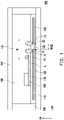
- FIG. 1 is a schematic partial cross-sectional view of an electronic device according to an embodiment of the disclosure.
- the electronic device 100 includes a substrate 110, a first metal layer 120, an electronic component 130, a cover layer 140, and an adhesive layer 150.
- the first metal layer 120 is formed on the substrate 110.
- the electronic component 130 is disposed on the substrate 110 and is electrically connected to the first metal layer 120.
- the adhesive layer 150 is adhered to the substrate 110 and the cover layer 140.
- the cover layer 140 and the substrate 110 are disposed opposite to each other, and the first metal layer 120 and the electronic component 130 are located between the substrate and the cover layer 140.
- the adhesive layer 150 is adapted to bring the substrate 110 and the cover layer 140 together.
- the adhesive layer 150 is disposed on the periphery of the electronic device 100 and may be in a ring-shaped pattern (e.g., from the top view). In this way, the substrate 110, the cover layer 140, and the adhesive layer 150 surround the electronic component 130 and the first metal layer 120. By encapsulating the electronic component 130, the first metal layer 120, or other components formed on the substrate, the external influence from moisture or oxygen on the electronic component 130 may be reduced, thereby improving the reliability of the electronic device, but the disclosure is not limited thereto. In other embodiments, the electronic component 130 may be covered in other ways, such that at least one of the cover layer 140 and the adhesive layer 150 may be omitted.
- an encapsulation layer may be formed on the substrate 110 to surround the electronic components 130 or other components formed on the substrate, and at least one of the cover layer 140 and the adhesive layer 150 may be thus omitted, but the disclosure is not limited thereto.
- the material of the encapsulation layer may be light-transmitting or opaque.
- the substrate 110 may be a glass substrate, a ceramic substrate, a plastic substrate, or other elements with sufficient supporting properties.
- the material of the substrate 110 may include glass, quartz, organic polymer, opaque/reflective material (e.g., conductive material, metal, wafer, ceramic, or other materials applicable), a single layer or a stack of one of the applicable materials, or a stack or a mixture of at least two of the above materials, but the disclosure is not limited thereto.
- the plastic substrates that may be used as the substrate 110 include, but are not limited to, polyimide substrates, liquid crystal polymer substrates, cyclo olefin polymer (COP) substrates, polymethyl methacrylate (PMMA) substrate, polycarbonate (PC) substrate, poly tetra fluoroethylene, (PTFE), but the disclosure is not limited thereto.
- COP cyclo olefin polymer
- PMMA polymethyl methacrylate
- PC polycarbonate
- PTFE poly tetra fluoroethylene
- the electronic device 100 is a device capable of receiving various electromagnetic wave bandwidths, such as an antenna device.
- the first metal layer 120 is, for example, a ground metal layer, and the first metal layer 120 is disposed on the substrate 110, occupying a large area of the substrate. For example, the first metal layer 120 may occupy 80% to 90% of the area of the substrate 110.
- the first metal layer 120 may be stacked on the substrate 110.
- the first metal layer 120 may be formed on the substrate 110 by deposition, printing, electroplating, or the like.
- the first metal layer 120 may be formed on the substrate 110 by sputtering, evaporation, or the like.
- the material of the first metal layer 120 includes copper, tin, nickel, or other metals.
- the first metal layer 120 may be a copper layer electroplated on the substrate 110, but the disclosure is not limited thereto.
- the first metal layer 120 may have a plurality of openings 122, but FIG. 1 only shows one opening 122 for convenience of description.
- the first metal layer 120 on both sides of the opening 122 is continuous and electrically grounded.
- the openings 122 may be closed patterns and are surrounded by the material of the first metal layer 120.
- the width W122 of the opening 122 may be related to the wavelength of the electromagnetic wave signal receivable/transmittable by the electronic device 100. Therefore, the width W122 of the opening 122 may be determined based on the function of the electronic device 100 as required.
- the location of the electronic component 130 may correspond to the opening 122 of the first metal layer 110. Specifically, in the normal direction DN of the substrate 110, the electronic components 130 overlap the openings 122. In FIG. 1 , a first direction D1 is perpendicular to the normal direction DN, the electronic component 130 has a width W in the first direction D1, the opening 122 has a width W122 in the first direction D1, and the width W is greater than the width W122. In some embodiments, the electronic component 130 may overlap the first metal layer 120 on one side S1 of the opening 122 and also overlap the first metal layer 120 on the other side S2 of the opening 122. The electronic component 130 may be electrically connected to the first metal layer 120.
- the electronic component 130 is electrically connected to the first metal layer 120 through the corresponding bonding pads P1 and P2, the electronic component 130 is disposed on the substrate 110.
- the electronic component 130 may be bonded and fixed to the substrate 110 through pads or adhesive, but the disclosure is not limited thereto.
- electronic components 130 may include capacitors, semiconductor wafers, and the like.
- the electronic component 130 may be, for example, a varactor or an integrated circuit (IC) chip, but the disclosure is not limited thereto.
- the cover layer 140 may have a plate-like structure, but the disclosure is not limited thereto.
- the cover layer 140 may be a glass substrate, a ceramic substrate, a polyimide substrate, a liquid crystal polymer substrate, a cyclo olefin polymer (COP) substrate, an acrylic substrate (e.g., a polymethyl methacrylate (PMMA) substrate), a polycarbonate (PC) substrate, poly tetra fluoroethylene (PTFE), etc.
- the cover layer 140 and the substrate 110 may include the same material or of different materials.
- the cover layer 140 may contact the electronic components 130.
- the cover layer 140 may contact an upper surface of the electronic component 130, such that the electronic component 130 maintains the distance between the substrate 110 and the cover layer 140, but the disclosure is not limited thereto.
- the adhesive layer 150 is used for adhering the substrate 110 and the cover layer 140, that is, the substrate 110 and the cover layer 140 may be fixed to each other through the adhesive layer 150.
- the adhesive layer 150 may be disposed on the periphery of the electronic device 100. Therefore, the substrate 110, the cover layer 140, and the adhesive layer 150 enclose a space, and components such as the first metal layer 120 and the electronic component 130 may be disposed in the space surrounded by the substrate 110, the cover layer 140, and the adhesive layer 150.
- the adhesive layer 150 may include a sealant material or other adhesive materials.
- the adhesive layer 150 may include a curable material, such as heat-curable glue, light-curable glue, and the like.
- the outer sidewalls of the adhesive layer 150, the substrate 110, and the cover layer 140 may or may not be aligned with one another.
- the cover layer 140 may be omitted and the electronic component 130 is directly covered with the adhesive layer 150, such that the electronic component 130 is covered by the adhesive layer 150 and the substrate 110.
- the electronic device 100 further includes a transistor 160.
- the transistor 160 may be formed on the substrate 110 as shown in FIG. 1 , but the disclosure is not limited thereto. In other embodiments, the transistor 160 may be formed on the cover layer 140.
- the transistor 160 may be electrically connected to the electronic component 130 to adjust or control the characteristics of the electronic component 130. For example, when the electronic component 130 is a varactor, the electronic component 130 may be electrically connected to the transistor 160 to adjust and control the capacitance of the electronic component 130 through the transistor 160. In this way, the capacitance of the transistor 160 can determine the frequency of the electromagnetic wave signal received/transmitted by the electronic device 100.
- the electronic device 100 is a device capable of receiving/transmitting electromagnetic wave signals of different frequencies.
- the transistor 160 may be a thin film transistor (TFT), a separately packaged transistor, or other types of transistors. Take a thin film transistor as an example.
- the transistor 160 may a stack of multiple layers like a semiconductor layer, a multi-layer conductive layer, and a multi-layer insulating layer.
- the electronic device 100 further includes a second metal layer 170 formed on the substrate 110.
- the second metal layer 170 is adapted to connect the electronic component 130 electrically to the transistor 160.
- the first metal layer 120 for the fabrication process and the material of the second metal layer 170, but the disclosure is not limited thereto.
- the second metal layer 170 and the first metal layer 120 may include the same material or of different materials.
- the electronic device 100 further includes a bonding pad P3 formed on the substrate 110, and the second metal layer 170 extends between the bonding pad P3 and the transistor 160.
- the second metal layer 170 is disposed between at least one of the bonding pads (for example, P3) and the transistor 160, but the disclosure is not limited thereto.
- the electronic component 130 may be connected to the bonding pad P3 and is electrically connected to the transistor 160 through the bonding pad P3 and the second metal layer 160.
- the electronic component 130 may be electrically connected to the first metal layer 120 through the bonding pads P1 and P2 and to the second metal layer 170 and the transistor 160 through the bonding pads P3, and thus the electronic component 130 may have three contacts, but the disclosure is not limited thereto.
- the bonding pads P1, the bonding pads P2, and the bonding pads P3 are, for example, solder, but the disclosure is not limited thereto.
- the second metal layer 170 and the transistor 160 may be formed on the cover layer 140, and then the substrate 110 and the cover layer 140 may be joined through the adhesive layer 150, but the disclosure is not limited thereto.
- the first metal layer 120 is disposed between the second metal layer 170 and the substrate 110, and as shown in FIG. 1 , the electronic device 100 further includes an insulating layer IL disposed between the first metal layer 120 and the second metal layer 170.
- the insulating layer IL may include insulating materials such as inorganic insulating materials and organic insulating materials.
- the insulating layer IL may be a multilayer structure layer including multiple insulating materials stacked together.
- Inorganic insulating materials include, for example, silicon oxide (SiO x ), silicon nitride (SiN x ), silicon oxide nitride (SiO x N y ), and inorganic insulating materials include, for example, polyimide, photoresist, planar layer materials, but the disclosure is not limited thereto.
- components such as electronic components 130 and transistors 160 are disposed between the substrate 110 and the cover layer 140, and the substrate 110 and the cover layer 140 are adhered to the two opposite sides of the adhesive layer 150, which forms a configuration that encloses the electronic component 130 and the transistor 160 in the space surrounded by the adhesive layer 150, the substrate 110, and the cover layer 140 that shield the electronic component 130 and the transistor 160 from damage.
- the electronic device 100 may further include a filler 180. The filler 180 is interposed between the substrate 110 and the cover layer 140.
- the filler 180 may include a material with a low dielectric constant (Dk) or a material with a low dielectric loss (Df), and the dielectric loss coefficient of the filler 180 is greater than 0 and less than or equal to 4 at high frequencies (e.g., at 1 GHz). In some embodiments, the dielectric loss coefficient of the filler 180 is, for example, greater than 0 and less than or equal to 3.5, but the disclosure is not limited thereto.
- the propagation delay of the signal depends on the size of the dielectric constant, the size of the dielectric loss coefficient, and the structure of the transmission line.
- a substrate material with a low dielectric constant can reduce the propagation delay of the signal, or reduce the coupling capacitance between the wires, thereby reducing the cross talk between the signals, but the disclosure is not limited thereto.
- the configuration of the filler 180 in some embodiments does not affect the electrical properties of the electronic component 130 and the transmission and reception of electromagnetic waves by the electronic device 100.
- the filler 180 may be air or other gas (e.g., inert gas) in some embodiments.
- the filler 180 may be glue in some embodiments.
- the filler 180 may be an Ajinomoto build-up film (ABF) in some embodiments.
- the filler 180 may be bismaleimide-triazine (BT) in some embodiments.
- the filler 180 may include a liquid material in some embodiments.
- the filler 180 may fill the volume between the substrate 110 and the cover layer 140, but the disclosure is not limited thereto.
- electronic components such as the electronic component 130 and the transistor 160 may be encapsulated by the substrate 110, the cover layer 140, the adhesive layer 150, and the filler 180, such that the electronic components 130 and the transistor 160 may not be easily damped or oxidized, and therefore not easily damaged.
- the electronic device 100 may be a packaged device capable of transceiving electromagnetic waves of multiple frequencies.
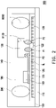
- FIG. 2 is a schematic partial cross-sectional view of an electronic device according to an embodiment of the disclosure.
- the electronic device 200 of FIG. 2 is substantially similar to the electronic device 100 of FIG. 1 , and the same reference numerals in the two embodiments may denote the same and/or similar elements, and one may be the reference of the other.
- the electronic device 200 includes a substrate 110, a first metal layer 120, an electronic component 130, a cover layer 140, an adhesive layer 150, a transistor 160, a second metal layer 170, a filler 180, and an insulating layer IL.
- the electronic device 200 further includes a spacer 290.
- the spacer 290 is disposed between the substrate 110 and the cover layer 140.
- the spacer 290 maintains a distance between the substrate 110 and the cover layer 140, such that the cover layer 140 does not contact and/or press against the electronic component 130.
- the height H290 of the spacer 290 may be greater than the height H130 of the electronic component 130.
- the height H130 is, for example, 0.2 mm to 0.5 mm.
- the height H290 of the spacer 290 is, for example, on the order of millimeters or sub-millimeters.
- the spacers 290 may be spherical, and the spacers 290 may be distributed in the electronic device 100 regularly or randomly.
- the spacer 290 may be other forms of spacers in other embodiments.
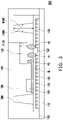
- FIG. 3 is a schematic partial cross-sectional view of an electronic device according to an embodiment of the disclosure.
- the electronic device 300 of FIG. 2 is substantially similar to the electronic device 200 of FIG. 2 , and the same referential numerals may represent the same and/or similar elements in the two embodiments.
- the electronic device 300 includes a substrate 110, a first metal layer 120, an electronic component 130, a cover layer 140, an adhesive layer 150, a transistor 160, a second metal layer 170, a filler 180, a spacer 390, and an insulating layer IL.
- the electronic device 300 is different from the electronic device 200 mainly specifically in the aspect of the spacer 390, and the rest of the elements of the electronic device 300 may be referred to the descriptions of FIG. 1 and FIG. 2 .
- the spacer 390 is, for example, a columnar spacer.
- the width W390 of the spacer 390 may vary from one end to the other, but the disclosure is not limited thereto.
- the width W390 of the spacer 390 illustrated in FIG. 2 gradually decreases from an end close to the substrate 110 to an end close to the cover layer 140, and the spacer 390 may be, for example a trapezoid, but the disclosure is not limited thereto.
- the width W390 of the spacer 390 may gradually increase from an end close to the substrate 110 to an end close to the cover layer 140, and the spacer 390 may be, for example, an inverted trapezoid, but the disclosure is not limited thereto.
- the width W390 of the spacer 390 may remain identical from an end close to the substrate 110 to an end close to the cover layer 140.
- the height H390 of the spacer 390 may refer to the height H290 of the spacer 290 in FIG. 1 .
- the height H390 of the spacer 390 may be greater than the height H130 of the electronic component 130.
- the height H390 of the spacer 390 may be on the order of millimeters or sub-millimeters.
- the spacer 390 may be fabricated by lithography.
- the material of the spacer 390 includes, for example, a photoresist material.
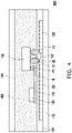
- FIG. 4 is a schematic partial cross-sectional view of an electronic device according to an embodiment of the disclosure.
- the electronic device 400 of FIG. 4 is substantially similar to the electronic device 100 of FIG. 1 , and the same reference numerals in the two embodiments may denote the same and/or similar elements, and one may be the reference of the other.
- the electronic device 400 includes a substrate 110, a first metal layer 120, an electronic component 130, a cover layer 140, an adhesive layer 450, a transistor 160, a second metal layer 170, and an insulating layer IL.
- the electronic device 400 is different from the electronic device 100 mainly in that the adhesive layer 450 of the electronic device 400 replaces the adhesive layer 150 and the filler 180 in FIG. 1 . As shown in FIG.
- the adhesive layer 450 is continuously disposed between the substrate 110 and the cover layer 140, and directly contacts the electronic component 130 and the transistor 160.
- the adhesive layer 450 may have a low dielectric constant (Dk) or a low dielectric loss (Df).
- the adhesive layer 450 may include silicone, acrylic, or other glues.
- the adhesive layer 450 may be an Ajinomoto build-up film (ABF) or a bismaleimide-triazine (BT).
- the adhesive layer 450 may fill the volume between the substrate 110 and the cover layer 140, but the disclosure is not limited thereto.
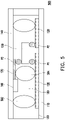
- FIG. 5 is a partial cross-sectional schematic diagram of an electronic device according to an embodiment of the disclosure.
- the electronic device 500 of FIG. 5 is substantially similar to the electronic device 100 of FIG. 1 , and the same reference numerals in the two embodiments may denote the same and/or similar elements, and one may be the reference of the other.
- the electronic device 500 includes a substrate 110, a first metal layer 120, an electronic component 130, a cover layer 140, an adhesive layer 150, a transistor 160, a second metal layer 170, and a filler 180.
- the electronic device 500 is different from the electronic device 100 mainly in that the transistor 160 and the second metal layer 170 of the electronic device 500 are formed on the cover layer 140, and that the electronic device 500 further includes a spacer 592 and a spacer 594.
- the electronic component 130 may be connected through the bonding pad P3to the second metal layer 170 formed on the cover layer 140, the second metal layer 170 extends between the transistor 160 and the bonding pad P3, and the transistor 160 is electrically connected to the electronic component 130 through the second metal layer 170.
- the spacer 592 is disposed between the substrate 110 and the cover layer 140 to maintain the distance between the substrate 110 and the cover layer 140, and the spacer 594 is disposed between the first metal layer 120 and the second metal layer 170 to avoid short circuit between the two metal layers.
- the height of the spacer 592 may be greater than the height of the spacer 594.
- the spacer 592 and the spacer 594 are shown as spherical spacers in FIG. 5 as an example, but they are not limited thereto. In some embodiments, the spacer 592 and the spacer 594 may be columnar spacers (such as the spacers 390 in FIG. 3 ).
- FIG. 6 is a schematic partial top view of an electronic device according to an embodiment of the disclosure.
- FIG. 6 shows some of the components in the electronic device 600 for illustration. It should be understood that the electronic device 600 may include other components described in the foregoing embodiments, including the components not proposed herein.
- the electronic device 600 in FIG. 6 includes a first metal layer 120, a plurality of electronic components 130, a plurality of transistors 160, a second metal layer 170, a plurality of signal lines SL1, and a plurality of signal lines SL2.
- FIG. 6 may serve as an embodiment of the top view of the first metal layer 120, the electronic component 130, the transistor 160, and the second metal layer 170 in FIG. 1 to FIG. 5 , but the disclosure is not limited thereto.
- the first metal layer 120 has a plurality of openings 122.
- the width W122 of the opening 122 may be related to the wavelength of the electromagnetic wave to be transmitted and received by the electronic device 600.
- the opening 122 may have an elongated shape with a length L122 greater than a width W122.
- the openings 122 are shown to be disposed parallel to each other in FIG. 6 as an example, but the disclosure is not limited thereto.
- the extending directions of the lengths L122 of the openings 122 may be disposed in different directions. For example, the extending directions of two adjacent openings 122 may intersect.
- the electronic components 130 are respectively disposed to correspond to one of the openings 122, and each electronic component 130 may overlap one of the openings 122. In other words, in the top view shown in FIG. 6 , the area of the electronic component 130 may overlap the area surrounded by the outline of the opening 122.
- each electronic component 130 may be electrically connected to the first metal layer 120 through corresponding bonding pads (e.g., the aforementioned bonding pads P1 and P2).
- the second metal layer 170 may include a plurality of independent patterns EE, and each electronic component 130 may be electrically connected to a corresponding one of the transistors 160 through one of the patterns EE of the second metal layer 170. As such, each electronic component 130 may be independently controlled by one transistor 160.
- the signal lines SL1 each extend along the first direction D1, and the signal lines SL2 each extend along the second direction D2.
- the signal lines SL1 and SL2 are disposed alternately.
- the signal line SL1 transmits one of the scan signal and the data signal
- the signal line SL2 transmits the other one of the scan signal and the data signal.
- Each transistor 160 may be connected to one of the signal lines SL1 and one of the signal lines DL2.
- the signal line SL1, the signal line SL2, and the transistor 160 may thus form an active device array.
- the signal line SL1 and the signal line SL2 may be disposed in different conductive layers, and the two conductive layers are separated by corresponding insulating layers.
- one of the signal line SL1 and the signal line SL2 may be in the same layer as the second metal layer 170, but the disclosure is not limited thereto.
- the transistor 160 may be a thin film transistor composed of semiconductor layers, multilayer conductive layers, etc., and the conductive layer in the transistor 160 may be the same layer as at least one of the signal line SL1, the signal line SL2, and the second metal layer 170.
- electronic components such as the electronic component are disposed between the substrate and the cover layer to protect the electronic components from moisture and/or oxidation.
- the electronic device of the embodiment of the disclosure further utilizes a filler or an adhesive layer to encapsulate the electronic components, which helps improve the protection of the electronic components.
Landscapes
- Structures Or Materials For Encapsulating Or Coating Semiconductor Devices Or Solid State Devices (AREA)
- Non-Metallic Protective Coatings For Printed Circuits (AREA)
- Production Of Multi-Layered Print Wiring Board (AREA)
Abstract
Description
- The disclosure relates to an electronic device.
- Electronic devices are universal with its application in various fields, and outdoor spaces are one where the electronic devices may be applied and installed. Therefore, the environmental reliability of electronic devices is an issue to be paid attention to.
- According to an embodiment of the present disclosure, an electronic device includes a substrate, a first metal layer, an electronic component, a cover layer, and an adhesive layer. The first metal layer is formed on the substrate. The electronic component is disposed on the substrate and electrically connected to the first metal layer. The adhesive layer is adhered to the substrate and the cover layer.
- To make the above-mentioned features and advantages of the disclosure more comprehensible, the following specific embodiments are described in detail with reference to the following drawings.
- The drawings are included for further understanding of the disclosure, and the drawings are incorporated into this specification and constitute a part of this specification. The drawings illustrate the embodiments of the disclosure, and together with the description are used to explain the principles of the disclosure.
-
FIG. 1 is a schematic partial cross-sectional view of an electronic device according to an embodiment of the disclosure. -
FIG. 2 is a schematic partial cross-sectional view of an electronic device according to an embodiment of the disclosure. -
FIG. 3 is a schematic partial cross-sectional view of an electronic device according to an embodiment of the disclosure. -
FIG. 4 is a schematic partial cross-sectional view of an electronic device according to an embodiment of the disclosure. -
FIG. 5 is a partial cross-sectional schematic diagram of an electronic device according to an embodiment of the disclosure. -
FIG. 6 is a schematic partial top view of an electronic device according to an embodiment of the disclosure. - The present disclosure may be understood by referring to the following detailed description in conjunction with the drawings. For readers' understanding and the brevity of the drawings, the drawings of this disclosure only depict part of a light-emitting device, and the specific elements in the drawings are not drawn according to actual scale. In addition, the number and size of each element in the drawings are only for schematic purposes and do not limit the scope of the disclosure.
- Throughout the disclosure and the claims, certain words are used to refer to specific elements. Those skilled in the art should understand that electronic device manufacturers may refer to the same components by different names. This article does not intend to distinguish those elements with the same function but different names. In the following description and claims, the words "having" and "including" are open-ended words, so they should be interpreted as meaning "including but the disclosure is not limited to." Therefore, when the terms "including," "containing" and/or "having" are used in the description of the present disclosure, they specify the existence of corresponding features, regions, steps, operations, and/or components, but do not exclude one or more existence of corresponding features, regions, steps, operations, and/or components.
- When an element or a film layer is referred to as being "on" or "connected" to another element or film layer, it may be directly on or directly connected to the other element or film layer. Or, there may be an element or film layer intervening between the two (in the case of indirect contact). Conversely, when an element is referred to as being "directly" on or "directly connected" to another element or film layer, there is no element or film layer intervening between the two. In addition, when an element is referred to as "on another element," the two are above or below each other in the top view direction, and this element may be above or below the other element, and this above-or-below relationship depends on the orientation of the device.
- Although the terms "first," "second," "third," and the likes may be used to describe various constituent elements, the constituent elements are not limited to these terms. This term is only used to distinguish a single constituent element from other constituent elements in the specification. The same terms may not be used in the claims, and the elements in the claims may be replaced with first, second, third and the likes according to the order declared by the elements in the claims. Therefore, in the following description, the first constituent element may be the second constituent element in the claims.
- In the text, the terms "about," "approximately," "substantially," and "substantially" usually mean it is within 10%, 5%, 3%, or 2%, 1%, or 0.5% of a given value or range. The quantity given here is an approximate quantity. In other words, in the absence of a specific description for the terms "about," "approximately," "substantially" or "approximately," "about," and "approximately," the meaning of "substantially" and "substantially" is still implied. In addition, the descriptions "ranging from the first value to the second value" and "between the first value and the second value" imply that the range includes the first value, the second value, and other values in between.
- In some embodiments of the present disclosure, terms related to bonding and connection, such as "connected," "interconnected," unless specifically defined, it mean that two structures are in direct contact, or that two structures are not in direct contact and there are other structures located between these two structures. And the terms about joining and connecting can also include the case where both structures are movable or both structures are fixed. In addition, the term "coupled" includes any direct and indirect electrical connection means.
- In this disclosure, the thickness, length, and width may be measured by using an optical microscope, and the thickness may be measured by a cross-sectional image in an electron microscope, but it is not limited thereto. In addition, there may be a certain margin in any two values or directions used for comparison. If the first value is equal to the second value, it implies that there may be a margin of about 10% between the first value and the second value; if the first direction is perpendicular to the second direction, the angle between the first direction and the second direction may be between 80 degrees and 100degrees; if the first direction is parallel to the second direction, the angle between the first direction and the second direction may be between 0 degrees and 10 degrees. Without further definitions, all terms (technical and scientific terms included) used herein have the same meanings as commonly understood by those skilled in the art to which this disclosure belongs. It is understandable that these terms, such as those defined in commonly used dictionaries, should be interpreted as having meaning consistent with the relevant technology and the background or context of this disclosure, and should not be interpreted in an idealized or excessively formal way, unless a specific definition is provided in the embodiment of the present disclosure.
- The display panel of the present disclosure may be applied to electronic devices such as display devices, antenna devices (e.g., liquid crystal antennas), sensing devices, light-emitting devices, touch devices, splicing devices, or any combination of the foregoing, but the disclosure is not limited thereto. The electronic device may include a bendable and flexible electronic device. The appearance of the electronic device may include a rectangle, a circle, a polygon, a shape with a curved edge, or other suitable shapes. The display device may, for example, include light-emitting diodes (LEDs), liquid crystal (fluorescence), phosphor (phosphor), quantum dot (QD), other suitable materials, or a combination of the foregoing, but the disclosure is not limited thereto. Light-emitting diodes may include, for example, organic light-emitting diodes (OLED), inorganic light-emitting diodes, sub-millimeter light-emitting diodes (mini LEDs), micro LEDs, or quantum dot light-emitting diodes (QLED or QDLED), other suitable materials, or any combination of the above, but the disclosure is not limited thereto. The appearance of the electronic device may have rectangular, circular, polygonal shape, a shape with curved edges, or other suitable shapes. The electronic device may have peripheral systems such as a driving system, a control system, a light source system, a shelf system, to support a display device, an antenna device, or a splicing device. Hereinafter, the display panel will be adapted to illustrate the content of the disclosure, but the disclosure is not limited thereto.
- It should be understood that the following embodiments may be substituted, reorganized, and mixed to complete other embodiments without departing from the spirit of the present disclosure. The features between the embodiments may be mixed and matched arbitrarily as long as they do not violate or in conflict with the spirit of the disclosure.
- Reference will now be made in detail to the exemplary embodiments of the present disclosure, and examples of the exemplary embodiments are illustrated in the drawings. The same reference symbols may be used to denote the same or similar parts in the drawings and the description.
-
FIG. 1 is a schematic partial cross-sectional view of an electronic device according to an embodiment of the disclosure. As shown inFIG. 1 , theelectronic device 100 includes asubstrate 110, afirst metal layer 120, anelectronic component 130, acover layer 140, and anadhesive layer 150. Thefirst metal layer 120 is formed on thesubstrate 110. Theelectronic component 130 is disposed on thesubstrate 110 and is electrically connected to thefirst metal layer 120. Theadhesive layer 150 is adhered to thesubstrate 110 and thecover layer 140. Thecover layer 140 and thesubstrate 110 are disposed opposite to each other, and thefirst metal layer 120 and theelectronic component 130 are located between the substrate and thecover layer 140. Theadhesive layer 150 is adapted to bring thesubstrate 110 and thecover layer 140 together. In some embodiments, theadhesive layer 150 is disposed on the periphery of theelectronic device 100 and may be in a ring-shaped pattern (e.g., from the top view). In this way, thesubstrate 110, thecover layer 140, and theadhesive layer 150 surround theelectronic component 130 and thefirst metal layer 120. By encapsulating theelectronic component 130, thefirst metal layer 120, or other components formed on the substrate, the external influence from moisture or oxygen on theelectronic component 130 may be reduced, thereby improving the reliability of the electronic device, but the disclosure is not limited thereto. In other embodiments, theelectronic component 130 may be covered in other ways, such that at least one of thecover layer 140 and theadhesive layer 150 may be omitted. For example, an encapsulation layer may be formed on thesubstrate 110 to surround theelectronic components 130 or other components formed on the substrate, and at least one of thecover layer 140 and theadhesive layer 150 may be thus omitted, but the disclosure is not limited thereto. The material of the encapsulation layer may be light-transmitting or opaque. - The
substrate 110 may be a glass substrate, a ceramic substrate, a plastic substrate, or other elements with sufficient supporting properties. For example, the material of thesubstrate 110 may include glass, quartz, organic polymer, opaque/reflective material (e.g., conductive material, metal, wafer, ceramic, or other materials applicable), a single layer or a stack of one of the applicable materials, or a stack or a mixture of at least two of the above materials, but the disclosure is not limited thereto. Here, the plastic substrates that may be used as thesubstrate 110 include, but are not limited to, polyimide substrates, liquid crystal polymer substrates, cyclo olefin polymer (COP) substrates, polymethyl methacrylate (PMMA) substrate, polycarbonate (PC) substrate, poly tetra fluoroethylene, (PTFE), but the disclosure is not limited thereto. - In some embodiments, the
electronic device 100 is a device capable of receiving various electromagnetic wave bandwidths, such as an antenna device. Thefirst metal layer 120 is, for example, a ground metal layer, and thefirst metal layer 120 is disposed on thesubstrate 110, occupying a large area of the substrate. For example, thefirst metal layer 120 may occupy 80% to 90% of the area of thesubstrate 110. Thefirst metal layer 120 may be stacked on thesubstrate 110. In some embodiments, thefirst metal layer 120 may be formed on thesubstrate 110 by deposition, printing, electroplating, or the like. For example, in terms of deposition, thefirst metal layer 120 may be formed on thesubstrate 110 by sputtering, evaporation, or the like. The material of thefirst metal layer 120 includes copper, tin, nickel, or other metals. In some embodiments, thefirst metal layer 120 may be a copper layer electroplated on thesubstrate 110, but the disclosure is not limited thereto. - The
first metal layer 120 may have a plurality ofopenings 122, butFIG. 1 only shows oneopening 122 for convenience of description. In some embodiments, thefirst metal layer 120 on both sides of theopening 122 is continuous and electrically grounded. In other words, theopenings 122 may be closed patterns and are surrounded by the material of thefirst metal layer 120. The width W122 of theopening 122 may be related to the wavelength of the electromagnetic wave signal receivable/transmittable by theelectronic device 100. Therefore, the width W122 of theopening 122 may be determined based on the function of theelectronic device 100 as required. - The location of the
electronic component 130 may correspond to theopening 122 of thefirst metal layer 110. Specifically, in the normal direction DN of thesubstrate 110, theelectronic components 130 overlap theopenings 122. InFIG. 1 , a first direction D1 is perpendicular to the normal direction DN, theelectronic component 130 has a width W in the first direction D1, theopening 122 has a width W122 in the first direction D1, and the width W is greater than the width W122. In some embodiments, theelectronic component 130 may overlap thefirst metal layer 120 on one side S1 of theopening 122 and also overlap thefirst metal layer 120 on the other side S2 of theopening 122. Theelectronic component 130 may be electrically connected to thefirst metal layer 120. Specifically, theelectronic component 130 is electrically connected to thefirst metal layer 120 through the corresponding bonding pads P1 and P2, theelectronic component 130 is disposed on thesubstrate 110. In some embodiments, theelectronic component 130 may be bonded and fixed to thesubstrate 110 through pads or adhesive, but the disclosure is not limited thereto. In some embodiments,electronic components 130 may include capacitors, semiconductor wafers, and the like. Theelectronic component 130 may be, for example, a varactor or an integrated circuit (IC) chip, but the disclosure is not limited thereto. - The
cover layer 140 may have a plate-like structure, but the disclosure is not limited thereto. In some embodiments, thecover layer 140 may be a glass substrate, a ceramic substrate, a polyimide substrate, a liquid crystal polymer substrate, a cyclo olefin polymer (COP) substrate, an acrylic substrate (e.g., a polymethyl methacrylate (PMMA) substrate), a polycarbonate (PC) substrate, poly tetra fluoroethylene (PTFE), etc. Thecover layer 140 and thesubstrate 110 may include the same material or of different materials. In some embodiments, thecover layer 140 may contact theelectronic components 130. Furthermore, thecover layer 140 may contact an upper surface of theelectronic component 130, such that theelectronic component 130 maintains the distance between thesubstrate 110 and thecover layer 140, but the disclosure is not limited thereto. - The
adhesive layer 150 is used for adhering thesubstrate 110 and thecover layer 140, that is, thesubstrate 110 and thecover layer 140 may be fixed to each other through theadhesive layer 150. Theadhesive layer 150 may be disposed on the periphery of theelectronic device 100. Therefore, thesubstrate 110, thecover layer 140, and theadhesive layer 150 enclose a space, and components such as thefirst metal layer 120 and theelectronic component 130 may be disposed in the space surrounded by thesubstrate 110, thecover layer 140, and theadhesive layer 150. Theadhesive layer 150 may include a sealant material or other adhesive materials. Theadhesive layer 150 may include a curable material, such as heat-curable glue, light-curable glue, and the like. The outer sidewalls of theadhesive layer 150, thesubstrate 110, and thecover layer 140 may or may not be aligned with one another. In some embodiments, thecover layer 140 may be omitted and theelectronic component 130 is directly covered with theadhesive layer 150, such that theelectronic component 130 is covered by theadhesive layer 150 and thesubstrate 110. - In addition, the
electronic device 100 further includes atransistor 160. Thetransistor 160 may be formed on thesubstrate 110 as shown inFIG. 1 , but the disclosure is not limited thereto. In other embodiments, thetransistor 160 may be formed on thecover layer 140. Thetransistor 160 may be electrically connected to theelectronic component 130 to adjust or control the characteristics of theelectronic component 130. For example, when theelectronic component 130 is a varactor, theelectronic component 130 may be electrically connected to thetransistor 160 to adjust and control the capacitance of theelectronic component 130 through thetransistor 160. In this way, the capacitance of thetransistor 160 can determine the frequency of the electromagnetic wave signal received/transmitted by theelectronic device 100. In other words, theelectronic device 100 is a device capable of receiving/transmitting electromagnetic wave signals of different frequencies. In some embodiments, thetransistor 160 may be a thin film transistor (TFT), a separately packaged transistor, or other types of transistors. Take a thin film transistor as an example. Thetransistor 160 may a stack of multiple layers like a semiconductor layer, a multi-layer conductive layer, and a multi-layer insulating layer. - In some embodiments, the
electronic device 100 further includes asecond metal layer 170 formed on thesubstrate 110. Thesecond metal layer 170 is adapted to connect theelectronic component 130 electrically to thetransistor 160. Please refer to thefirst metal layer 120 for the fabrication process and the material of thesecond metal layer 170, but the disclosure is not limited thereto. Thesecond metal layer 170 and thefirst metal layer 120 may include the same material or of different materials. In addition, theelectronic device 100 further includes a bonding pad P3 formed on thesubstrate 110, and thesecond metal layer 170 extends between the bonding pad P3 and thetransistor 160. For example, thesecond metal layer 170 is disposed between at least one of the bonding pads (for example, P3) and thetransistor 160, but the disclosure is not limited thereto. Theelectronic component 130 may be connected to the bonding pad P3 and is electrically connected to thetransistor 160 through the bonding pad P3 and thesecond metal layer 160. In some embodiments, theelectronic component 130 may be electrically connected to thefirst metal layer 120 through the bonding pads P1 and P2 and to thesecond metal layer 170 and thetransistor 160 through the bonding pads P3, and thus theelectronic component 130 may have three contacts, but the disclosure is not limited thereto. The bonding pads P1, the bonding pads P2, and the bonding pads P3 are, for example, solder, but the disclosure is not limited thereto. For example, thesecond metal layer 170 and thetransistor 160 may be formed on thecover layer 140, and then thesubstrate 110 and thecover layer 140 may be joined through theadhesive layer 150, but the disclosure is not limited thereto. - The
first metal layer 120 is disposed between thesecond metal layer 170 and thesubstrate 110, and as shown inFIG. 1 , theelectronic device 100 further includes an insulating layer IL disposed between thefirst metal layer 120 and thesecond metal layer 170. The insulating layer IL may include insulating materials such as inorganic insulating materials and organic insulating materials. In some embodiments, the insulating layer IL may be a multilayer structure layer including multiple insulating materials stacked together. Inorganic insulating materials include, for example, silicon oxide (SiOx), silicon nitride (SiNx), silicon oxide nitride (SiOxNy), and inorganic insulating materials include, for example, polyimide, photoresist, planar layer materials, but the disclosure is not limited thereto. - In some embodiments, components such as
electronic components 130 andtransistors 160 are disposed between thesubstrate 110 and thecover layer 140, and thesubstrate 110 and thecover layer 140 are adhered to the two opposite sides of theadhesive layer 150, which forms a configuration that encloses theelectronic component 130 and thetransistor 160 in the space surrounded by theadhesive layer 150, thesubstrate 110, and thecover layer 140 that shield theelectronic component 130 and thetransistor 160 from damage. Additionally, theelectronic device 100 may further include afiller 180. Thefiller 180 is interposed between thesubstrate 110 and thecover layer 140. Thefiller 180 may include a material with a low dielectric constant (Dk) or a material with a low dielectric loss (Df), and the dielectric loss coefficient of thefiller 180 is greater than 0 and less than or equal to 4 at high frequencies (e.g., at 1 GHz). In some embodiments, the dielectric loss coefficient of thefiller 180 is, for example, greater than 0 and less than or equal to 3.5, but the disclosure is not limited thereto. The propagation delay of the signal depends on the size of the dielectric constant, the size of the dielectric loss coefficient, and the structure of the transmission line. For example, as the propagation time is proportional to the square root of the dielectric constant, a substrate material with a low dielectric constant can reduce the propagation delay of the signal, or reduce the coupling capacitance between the wires, thereby reducing the cross talk between the signals, but the disclosure is not limited thereto. It is possible that the configuration of thefiller 180 in some embodiments does not affect the electrical properties of theelectronic component 130 and the transmission and reception of electromagnetic waves by theelectronic device 100. Thefiller 180 may be air or other gas (e.g., inert gas) in some embodiments. Thefiller 180 may be glue in some embodiments. Thefiller 180 may be an Ajinomoto build-up film (ABF) in some embodiments. Thefiller 180 may be bismaleimide-triazine (BT) in some embodiments. Thefiller 180 may include a liquid material in some embodiments. Thefiller 180 may fill the volume between thesubstrate 110 and thecover layer 140, but the disclosure is not limited thereto. For example, there may be voids between theelectronic component 130 and the bonding pads P1 to P3, and the voids are not fully filled by thefiller 180, but the disclosure is not limited thereto. - In some embodiments, electronic components such as the
electronic component 130 and thetransistor 160 may be encapsulated by thesubstrate 110, thecover layer 140, theadhesive layer 150, and thefiller 180, such that theelectronic components 130 and thetransistor 160 may not be easily damped or oxidized, and therefore not easily damaged. In some embodiments, theelectronic device 100 may be a packaged device capable of transceiving electromagnetic waves of multiple frequencies. -
FIG. 2 is a schematic partial cross-sectional view of an electronic device according to an embodiment of the disclosure. Theelectronic device 200 ofFIG. 2 is substantially similar to theelectronic device 100 ofFIG. 1 , and the same reference numerals in the two embodiments may denote the same and/or similar elements, and one may be the reference of the other. Theelectronic device 200 includes asubstrate 110, afirst metal layer 120, anelectronic component 130, acover layer 140, anadhesive layer 150, atransistor 160, asecond metal layer 170, afiller 180, and an insulating layer IL. InFIG. 2 , theelectronic device 200 further includes aspacer 290. Thespacer 290 is disposed between thesubstrate 110 and thecover layer 140. In some embodiments, thespacer 290 maintains a distance between thesubstrate 110 and thecover layer 140, such that thecover layer 140 does not contact and/or press against theelectronic component 130. For example, the height H290 of thespacer 290 may be greater than the height H130 of theelectronic component 130. In some embodiments, when theelectronic component 130 is a semiconductor wafer, the height H130 is, for example, 0.2 mm to 0.5 mm. As such, the height H290 of thespacer 290 is, for example, on the order of millimeters or sub-millimeters. Thespacers 290 may be spherical, and thespacers 290 may be distributed in theelectronic device 100 regularly or randomly. Thespacer 290 may be other forms of spacers in other embodiments. -
FIG. 3 is a schematic partial cross-sectional view of an electronic device according to an embodiment of the disclosure. Theelectronic device 300 ofFIG. 2 is substantially similar to theelectronic device 200 ofFIG. 2 , and the same referential numerals may represent the same and/or similar elements in the two embodiments. Theelectronic device 300 includes asubstrate 110, afirst metal layer 120, anelectronic component 130, acover layer 140, anadhesive layer 150, atransistor 160, asecond metal layer 170, afiller 180, aspacer 390, and an insulating layer IL. Theelectronic device 300 is different from theelectronic device 200 mainly specifically in the aspect of thespacer 390, and the rest of the elements of theelectronic device 300 may be referred to the descriptions ofFIG. 1 andFIG. 2 . In some embodiments, thespacer 390 is, for example, a columnar spacer. The width W390 of thespacer 390 may vary from one end to the other, but the disclosure is not limited thereto. For example, the width W390 of thespacer 390 illustrated inFIG. 2 gradually decreases from an end close to thesubstrate 110 to an end close to thecover layer 140, and thespacer 390 may be, for example a trapezoid, but the disclosure is not limited thereto. In other embodiments, the width W390 of thespacer 390 may gradually increase from an end close to thesubstrate 110 to an end close to thecover layer 140, and thespacer 390 may be, for example, an inverted trapezoid, but the disclosure is not limited thereto. In some embodiments, the width W390 of thespacer 390 may remain identical from an end close to thesubstrate 110 to an end close to thecover layer 140. In addition, the height H390 of thespacer 390 may refer to the height H290 of thespacer 290 inFIG. 1 . For example, the height H390 of thespacer 390 may be greater than the height H130 of theelectronic component 130. The height H390 of thespacer 390 may be on the order of millimeters or sub-millimeters. In some embodiments, thespacer 390 may be fabricated by lithography. The material of thespacer 390 includes, for example, a photoresist material. -
FIG. 4 is a schematic partial cross-sectional view of an electronic device according to an embodiment of the disclosure. Theelectronic device 400 ofFIG. 4 is substantially similar to theelectronic device 100 ofFIG. 1 , and the same reference numerals in the two embodiments may denote the same and/or similar elements, and one may be the reference of the other. Theelectronic device 400 includes asubstrate 110, afirst metal layer 120, anelectronic component 130, acover layer 140, anadhesive layer 450, atransistor 160, asecond metal layer 170, and an insulating layer IL. Theelectronic device 400 is different from theelectronic device 100 mainly in that theadhesive layer 450 of theelectronic device 400 replaces theadhesive layer 150 and thefiller 180 inFIG. 1 . As shown inFIG. 4 , theadhesive layer 450 is continuously disposed between thesubstrate 110 and thecover layer 140, and directly contacts theelectronic component 130 and thetransistor 160. For example, at least a portion of a surface of thecover layer 140 is in contact with at least a portion of a surface of theelectronic component 130, but the disclosure is not limited thereto. Theadhesive layer 450 may have a low dielectric constant (Dk) or a low dielectric loss (Df). In some embodiments, theadhesive layer 450 may include silicone, acrylic, or other glues. In some embodiments, theadhesive layer 450 may be an Ajinomoto build-up film (ABF) or a bismaleimide-triazine (BT). Theadhesive layer 450 may fill the volume between thesubstrate 110 and thecover layer 140, but the disclosure is not limited thereto. For example, there may be voids VD between the bonding pads P1 to P3 below theelectronic component 130, and the voids are not fully filled by theadhesive layer 450, but the disclosure is not limited thereto. -
FIG. 5 is a partial cross-sectional schematic diagram of an electronic device according to an embodiment of the disclosure. Theelectronic device 500 ofFIG. 5 is substantially similar to theelectronic device 100 ofFIG. 1 , and the same reference numerals in the two embodiments may denote the same and/or similar elements, and one may be the reference of the other. Theelectronic device 500 includes asubstrate 110, afirst metal layer 120, anelectronic component 130, acover layer 140, anadhesive layer 150, atransistor 160, asecond metal layer 170, and afiller 180. Theelectronic device 500 is different from theelectronic device 100 mainly in that thetransistor 160 and thesecond metal layer 170 of theelectronic device 500 are formed on thecover layer 140, and that theelectronic device 500 further includes aspacer 592 and aspacer 594. - In some embodiments, the
electronic component 130 may be connected through the bonding pad P3to thesecond metal layer 170 formed on thecover layer 140, thesecond metal layer 170 extends between thetransistor 160 and the bonding pad P3, and thetransistor 160 is electrically connected to theelectronic component 130 through thesecond metal layer 170. In addition, thespacer 592 is disposed between thesubstrate 110 and thecover layer 140 to maintain the distance between thesubstrate 110 and thecover layer 140, and thespacer 594 is disposed between thefirst metal layer 120 and thesecond metal layer 170 to avoid short circuit between the two metal layers. The height of thespacer 592 may be greater than the height of thespacer 594. Thespacer 592 and thespacer 594 are shown as spherical spacers inFIG. 5 as an example, but they are not limited thereto. In some embodiments, thespacer 592 and thespacer 594 may be columnar spacers (such as thespacers 390 inFIG. 3 ). -
FIG. 6 is a schematic partial top view of an electronic device according to an embodiment of the disclosure.FIG. 6 shows some of the components in theelectronic device 600 for illustration. It should be understood that theelectronic device 600 may include other components described in the foregoing embodiments, including the components not proposed herein. Theelectronic device 600 inFIG. 6 includes afirst metal layer 120, a plurality ofelectronic components 130, a plurality oftransistors 160, asecond metal layer 170, a plurality of signal lines SL1, and a plurality of signal lines SL2.FIG. 6 may serve as an embodiment of the top view of thefirst metal layer 120, theelectronic component 130, thetransistor 160, and thesecond metal layer 170 inFIG. 1 to FIG. 5 , but the disclosure is not limited thereto. - The
first metal layer 120 has a plurality ofopenings 122. The width W122 of theopening 122 may be related to the wavelength of the electromagnetic wave to be transmitted and received by theelectronic device 600. Theopening 122 may have an elongated shape with a length L122 greater than a width W122. Theopenings 122 are shown to be disposed parallel to each other inFIG. 6 as an example, but the disclosure is not limited thereto. In some embodiments, the extending directions of the lengths L122 of theopenings 122 may be disposed in different directions. For example, the extending directions of twoadjacent openings 122 may intersect. - The
electronic components 130 are respectively disposed to correspond to one of theopenings 122, and eachelectronic component 130 may overlap one of theopenings 122. In other words, in the top view shown inFIG. 6 , the area of theelectronic component 130 may overlap the area surrounded by the outline of theopening 122. As described in the foregoing embodiments, eachelectronic component 130 may be electrically connected to thefirst metal layer 120 through corresponding bonding pads (e.g., the aforementioned bonding pads P1 and P2). In addition, thesecond metal layer 170 may include a plurality of independent patterns EE, and eachelectronic component 130 may be electrically connected to a corresponding one of thetransistors 160 through one of the patterns EE of thesecond metal layer 170. As such, eachelectronic component 130 may be independently controlled by onetransistor 160. - The signal lines SL1 each extend along the first direction D1, and the signal lines SL2 each extend along the second direction D2. The signal lines SL1 and SL2 are disposed alternately. In some embodiments, the signal line SL1 transmits one of the scan signal and the data signal, and the signal line SL2 transmits the other one of the scan signal and the data signal. Each
transistor 160 may be connected to one of the signal lines SL1 and one of the signal lines DL2. The signal line SL1, the signal line SL2, and thetransistor 160 may thus form an active device array. In addition, the signal line SL1 and the signal line SL2 may be disposed in different conductive layers, and the two conductive layers are separated by corresponding insulating layers. In some embodiments, one of the signal line SL1 and the signal line SL2 may be in the same layer as thesecond metal layer 170, but the disclosure is not limited thereto. In some embodiments, thetransistor 160 may be a thin film transistor composed of semiconductor layers, multilayer conductive layers, etc., and the conductive layer in thetransistor 160 may be the same layer as at least one of the signal line SL1, the signal line SL2, and thesecond metal layer 170. - In summary, in the electronic device according to the embodiments of the disclosure, electronic components such as the electronic component are disposed between the substrate and the cover layer to protect the electronic components from moisture and/or oxidation. In addition, the electronic device of the embodiment of the disclosure further utilizes a filler or an adhesive layer to encapsulate the electronic components, which helps improve the protection of the electronic components.
Claims (15)
- An electronic device (100, 200, 300, 400, 500, 600, 700), comprising:a substrate (110);a first metal layer (120), formed on the substrate (110);an electronic component (130), disposed on the substrate (110) and electrically connected to the first metal layer (120);a cover layer (140); andan adhesive layer (150), adhered to the substrate (110) and the cover layer (140).
- The electronic device (100, 200, 300, 400, 500, 600, 700) of claim 1, further comprising a transistor (160) formed on at least one of the substrate (110) and the cover layer (140) and electrically connected to the electronic component (130).
- The electronic device (100, 200, 300, 400, 500, 600, 700) of claim 2, further comprising a second metal layer (170) formed on the cover layer (140), wherein the transistor (160) is formed on the cover layer (140) and is electrically connected to the electronic component (130) through the second metal layer (170).
- The electronic device (100, 200, 300, 400, 500, 600, 700) of claim 3, further comprising bonding pads (PI, P2), wherein the electronic component (130) is connected to the bonding pads (PI, P2), and the second metal layer (170) is disposed between at least one of the bonding pads (PI, P2) and the transistor (160).
- The electronic device (100, 200, 300, 400, 500, 600, 700) of any of claims 1 to 4, further comprising a spacer (290, 390, 592) disposed between the substrate (110) and the cover layer (140).
- The electronic device (100, 200, 300, 400, 500, 600, 700) of claim 5, wherein a height of the spacer (290, 390, 592) is greater than a height of the electronic component (130).
- The electronic device (100, 200, 300, 400, 500, 600, 700) of any of claims 1 to 6, wherein the electronic component (130) contacts the cover layer (140).
- The electronic device (100, 200, 300, 400, 500, 600, 700) of any of claims 1 to 7, further comprising a filler interposed between the substrate (110) and the cover layer (140).
- The electronic device (100, 200, 300, 400, 500, 600, 700) of claim 8, wherein the filler (180) is air, glue, or an Ajinomoto build-up film.
- The electronic device (100, 200, 300, 400, 500, 600, 700) of claim 8, wherein the filler (180) comprises a material with low dielectric loss.
- The electronic device (100, 200, 300, 400, 500, 600, 700) of any of claims 1 to 10, further comprising bonding pads (PI, P2), wherein the electronic component (130) is electrically connected to the first metal layer (120) through the bonding pads (PI, P2).
- The electronic device (100, 200, 300, 400, 500, 600, 700) of any of claims 1 to 11, wherein the electronic component (130) is a varactor or an integrated circuit chip.
- The electronic device (100, 200, 300, 400, 500, 600, 700) of any of claims 1 to 12, wherein the adhesive layer (150) is continuously disposed between the substrate (110) and the cover layer (140), and the adhesive layer (150) directly contacts the electronic component (130).
- The electronic device (100, 200, 300, 400, 500, 600, 700) of any of claims 1 to 13, wherein the first metal layer (120) has a plurality of openings (122) and the electronic component (130) overlaps one of the openings (122), the opening (122) has an elongated shape, and a length of the opening (122) is greater than a width of the opening (122).
- The electronic device (100, 200, 300, 400, 500, 600, 700) of any of claims 1 to 14, wherein the adhesive layer (150) comprises a heat-curable glue or a light-curable glue.
Applications Claiming Priority (2)
| Application Number | Priority Date | Filing Date | Title |
|---|---|---|---|
| US202163221003P | 2021-07-13 | 2021-07-13 | |
| CN202210386206.7A CN115623678A (en) | 2021-07-13 | 2022-04-13 | Electronic device |
Publications (2)
| Publication Number | Publication Date |
|---|---|
| EP4120334A2 true EP4120334A2 (en) | 2023-01-18 |
| EP4120334A3 EP4120334A3 (en) | 2023-05-03 |
Family
ID=83115476
Family Applications (1)
| Application Number | Title | Priority Date | Filing Date |
|---|---|---|---|
| EP22181486.6A Pending EP4120334A3 (en) | 2021-07-13 | 2022-06-28 | Electronic device |
Country Status (2)
| Country | Link |
|---|---|
| US (1) | US12593725B2 (en) |
| EP (1) | EP4120334A3 (en) |
Families Citing this family (1)
| Publication number | Priority date | Publication date | Assignee | Title |
|---|---|---|---|---|
| TWI873574B (en) * | 2023-03-22 | 2025-02-21 | 友達光電股份有限公司 | Electronic device and manufacturing method of electronic device |
Family Cites Families (11)
| Publication number | Priority date | Publication date | Assignee | Title |
|---|---|---|---|---|
| JP3803596B2 (en) | 2002-03-14 | 2006-08-02 | 日本電気株式会社 | Package type semiconductor device |
| DE102011109006A1 (en) * | 2011-07-29 | 2013-01-31 | Epcos Ag | Housing for a semiconductor chip and semiconductor chip with a housing |
| EP3423152B1 (en) * | 2016-03-04 | 2021-12-22 | Accure Medical, LLC | Systems for treatment of fungus |
| DE102018101710A1 (en) * | 2018-01-25 | 2019-07-25 | Osram Opto Semiconductors Gmbh | OPTOELECTRONIC COMPONENT AND METHOD FOR PRODUCING AN OPTOELECTRONIC COMPONENT |
| US20200036081A1 (en) * | 2018-07-30 | 2020-01-30 | Innolux Corporation | Package structure and antenna device using the same |
| CN110858584A (en) * | 2018-08-23 | 2020-03-03 | 弘凯光电(深圳)有限公司 | Light emitting module and light emitting serial device |
| CN109887891B (en) * | 2019-03-08 | 2021-01-22 | 苏州通富超威半导体有限公司 | Package structure and method for forming the same |
| KR20200123572A (en) * | 2019-04-22 | 2020-10-30 | 삼성전기주식회사 | Electronic component module and method for fabricating the same |
| JP7271337B2 (en) * | 2019-06-27 | 2023-05-11 | 新光電気工業株式会社 | Electronic component device and method for manufacturing electronic component device |
| US20210043573A1 (en) | 2019-08-06 | 2021-02-11 | Intel Corporation | Thermal management in integrated circuit packages |
| US20210066162A1 (en) | 2019-08-30 | 2021-03-04 | Intel Corporation | Semiconductor package with attachment and/or stop structures |
-
2022
- 2022-06-21 US US17/844,744 patent/US12593725B2/en active Active
- 2022-06-28 EP EP22181486.6A patent/EP4120334A3/en active Pending
Also Published As
| Publication number | Publication date |
|---|---|
| US20230026864A1 (en) | 2023-01-26 |
| US12593725B2 (en) | 2026-03-31 |
| EP4120334A3 (en) | 2023-05-03 |
Similar Documents
| Publication | Publication Date | Title |
|---|---|---|
| US10325969B2 (en) | Display panel, fabrication method and display apparatus | |
| US9113545B2 (en) | Tape wiring substrate and chip-on-film package including the same | |
| KR20200141933A (en) | Electronic device and tiled electronic device | |
| US12593725B2 (en) | Electronic device | |
| EP4220289A1 (en) | Modulation device | |
| TWI823439B (en) | Backlight module and electronic device | |
| US20220028777A1 (en) | Chip on film package and display apparatus including the same | |
| TWI818509B (en) | Electronic device | |
| US12413185B2 (en) | Electronic device | |
| KR102921935B1 (en) | Chip on film package | |
| CN113725229B (en) | Display device | |
| TWI917766B (en) | Modulation device | |
| US20230421135A1 (en) | Modulation device | |
| US20230335563A1 (en) | Electronic device | |
| TWI917736B (en) | Electronic device | |
| US20240243069A1 (en) | Electronic device | |
| US20250234694A1 (en) | Electronic device | |
| TWI752508B (en) | Display device | |
| TWI843071B (en) | Electronic device | |
| US20240395991A1 (en) | Electronic device and tiled electronic device | |
| US20250234690A1 (en) | Electronic device and semiconductor chip thereof | |
| US20250351655A1 (en) | Electronic device | |
| TW202341378A (en) | Electronic device | |
| CN115441166A (en) | Electronic device | |
| KR20250120030A (en) | Light emitting device package and display device using same |
Legal Events
| Date | Code | Title | Description |
|---|---|---|---|
| PUAI | Public reference made under article 153(3) epc to a published international application that has entered the european phase |
Free format text: ORIGINAL CODE: 0009012 |
|
| STAA | Information on the status of an ep patent application or granted ep patent |
Free format text: STATUS: THE APPLICATION HAS BEEN PUBLISHED |
|
| AK | Designated contracting states |
Kind code of ref document: A2 Designated state(s): AL AT BE BG CH CY CZ DE DK EE ES FI FR GB GR HR HU IE IS IT LI LT LU LV MC MK MT NL NO PL PT RO RS SE SI SK SM TR |
|
| PUAL | Search report despatched |
Free format text: ORIGINAL CODE: 0009013 |
|
| AK | Designated contracting states |
Kind code of ref document: A3 Designated state(s): AL AT BE BG CH CY CZ DE DK EE ES FI FR GB GR HR HU IE IS IT LI LT LU LV MC MK MT NL NO PL PT RO RS SE SI SK SM TR |
|
| RIC1 | Information provided on ipc code assigned before grant |
Ipc: H01L 33/48 20100101ALN20230328BHEP Ipc: H01L 25/07 20060101ALN20230328BHEP Ipc: H01L 23/20 20060101ALN20230328BHEP Ipc: H01L 33/52 20100101ALI20230328BHEP Ipc: H10K 59/80 20230101ALI20230328BHEP Ipc: H01L 23/433 20060101ALI20230328BHEP Ipc: H01L 23/498 20060101ALI20230328BHEP Ipc: H01L 23/10 20060101ALI20230328BHEP Ipc: H01L 25/16 20230101ALI20230328BHEP Ipc: H01L 25/075 20060101ALI20230328BHEP Ipc: H01L 23/00 20060101ALI20230328BHEP Ipc: H01L 23/053 20060101ALI20230328BHEP Ipc: H01L 23/043 20060101AFI20230328BHEP |
|
| STAA | Information on the status of an ep patent application or granted ep patent |
Free format text: STATUS: REQUEST FOR EXAMINATION WAS MADE |
|
| 17P | Request for examination filed |
Effective date: 20231030 |
|
| RBV | Designated contracting states (corrected) |
Designated state(s): AL AT BE BG CH CY CZ DE DK EE ES FI FR GB GR HR HU IE IS IT LI LT LU LV MC MK MT NL NO PL PT RO RS SE SI SK SM TR |