EP4120298A1 - Capacitor module - Google Patents
Capacitor module Download PDFInfo
- Publication number
- EP4120298A1 EP4120298A1 EP21797156.3A EP21797156A EP4120298A1 EP 4120298 A1 EP4120298 A1 EP 4120298A1 EP 21797156 A EP21797156 A EP 21797156A EP 4120298 A1 EP4120298 A1 EP 4120298A1
- Authority
- EP
- European Patent Office
- Prior art keywords
- bus bar
- electrode
- insulating member
- case
- capacitor
- Prior art date
- Legal status (The legal status is an assumption and is not a legal conclusion. Google has not performed a legal analysis and makes no representation as to the accuracy of the status listed.)
- Pending
Links
Images














Classifications
-
- H—ELECTRICITY
- H01—ELECTRIC ELEMENTS
- H01G—CAPACITORS; CAPACITORS, RECTIFIERS, DETECTORS, SWITCHING DEVICES, LIGHT-SENSITIVE OR TEMPERATURE-SENSITIVE DEVICES OF THE ELECTROLYTIC TYPE
- H01G2/00—Details of capacitors not covered by a single one of groups H01G4/00-H01G11/00
- H01G2/02—Mountings
-
- H—ELECTRICITY
- H01—ELECTRIC ELEMENTS
- H01G—CAPACITORS; CAPACITORS, RECTIFIERS, DETECTORS, SWITCHING DEVICES, LIGHT-SENSITIVE OR TEMPERATURE-SENSITIVE DEVICES OF THE ELECTROLYTIC TYPE
- H01G2/00—Details of capacitors not covered by a single one of groups H01G4/00-H01G11/00
- H01G2/10—Housing; Encapsulation
-
- H—ELECTRICITY
- H01—ELECTRIC ELEMENTS
- H01G—CAPACITORS; CAPACITORS, RECTIFIERS, DETECTORS, SWITCHING DEVICES, LIGHT-SENSITIVE OR TEMPERATURE-SENSITIVE DEVICES OF THE ELECTROLYTIC TYPE
- H01G4/00—Fixed capacitors; Processes of their manufacture
- H01G4/002—Details
- H01G4/005—Electrodes
- H01G4/01—Form of self-supporting electrodes
-
- H—ELECTRICITY
- H01—ELECTRIC ELEMENTS
- H01G—CAPACITORS; CAPACITORS, RECTIFIERS, DETECTORS, SWITCHING DEVICES, LIGHT-SENSITIVE OR TEMPERATURE-SENSITIVE DEVICES OF THE ELECTROLYTIC TYPE
- H01G4/00—Fixed capacitors; Processes of their manufacture
- H01G4/002—Details
- H01G4/224—Housing; Encapsulation
-
- H—ELECTRICITY
- H01—ELECTRIC ELEMENTS
- H01G—CAPACITORS; CAPACITORS, RECTIFIERS, DETECTORS, SWITCHING DEVICES, LIGHT-SENSITIVE OR TEMPERATURE-SENSITIVE DEVICES OF THE ELECTROLYTIC TYPE
- H01G4/00—Fixed capacitors; Processes of their manufacture
- H01G4/002—Details
- H01G4/228—Terminals
-
- H—ELECTRICITY
- H01—ELECTRIC ELEMENTS
- H01G—CAPACITORS; CAPACITORS, RECTIFIERS, DETECTORS, SWITCHING DEVICES, LIGHT-SENSITIVE OR TEMPERATURE-SENSITIVE DEVICES OF THE ELECTROLYTIC TYPE
- H01G4/00—Fixed capacitors; Processes of their manufacture
- H01G4/32—Wound capacitors
-
- H—ELECTRICITY
- H01—ELECTRIC ELEMENTS
- H01G—CAPACITORS; CAPACITORS, RECTIFIERS, DETECTORS, SWITCHING DEVICES, LIGHT-SENSITIVE OR TEMPERATURE-SENSITIVE DEVICES OF THE ELECTROLYTIC TYPE
- H01G4/00—Fixed capacitors; Processes of their manufacture
- H01G4/38—Multiple capacitors, i.e. structural combinations of fixed capacitors
Definitions
- the present invention relates to a capacitor module.
- capacitor module in which one or a plurality of capacitors formed by winding or layering a dielectric film having a metal film on the surface are housed in a case, and bus bars are connected to electrodes at both ends of each capacitor.
- Patent Document 1 discloses a film capacitor in which a capacitor element and an electronic component are separately housed with a partition plate provided on a bottom surface of a case.
- Patent Document 1 Japanese Laid-Open Patent Publication No. 2001-210548
- the film capacitor described in JP 2001-210548 A still has room for improvement in terms of improvement in insulation.
- an object of the present invention is to provide a capacitor module with improved insulation.
- a capacitor module according to an aspect of the present invention includes:
- a capacitor module having two or more capacitor groups having different functions is known.
- each capacitor group is housed in one case and the case is filled with an insulating resin.
- Each capacitor group includes one or more capacitors.
- Each capacitor group is insulated by the insulating resin filled in the case.
- the present inventors have studied a configuration for improving insulation between capacitor groups in a capacitor module having two or more capacitor groups, and have reached the following invention.
- a capacitor module according to an aspect of the present invention includes:
- the insulating member may be disposed such that, in a direction from the opening toward the bottom surface, one end portion is positioned on the opening side relative to the electrode contact portion of the first bus bar and the electrode contact portion of the second bus bar, and an other end portion is positioned on the bottom surface side relative to the first electrode and the third electrode.
- a recess that receives the insulating member in a direction from the opening toward the bottom surface may be provided on an inner side surface of the case.
- the third bus bar may further have an extending portion extending to an outside of the case through the opening along a side surface of the case from the electrode contact portion of the third bus bar, and a through hole through which the insulating member passes may be provided in the extending portion.
- the insulating member may be positioned by being received by the third bus bar at one end on the bottom surface side of the through hole.
- the insulating member may include
- the side surface of the first capacitor and the side surface of the second capacitor may each include a pair of flat portions opposing each other and a pair of curved portions connecting the pair of flat portions, and the second portion of the insulating member may be disposed between the adjacent curved portions of the adjacent first capacitors and between the adjacent curved portions of the adjacent second capacitors.
- the second portion of the insulating member may have a protrusion, and the protrusion may be inserted into a hole provided in each of the first bus bar and the second bus bar.
- the second portion of the insulating member may have a recess
- the capacitor module may further comprise a screw inserted into a hole provided in each of the first bus bar and the second bus bar and the recess.
- the bottom surface of the case may be flat.
- Fig. 1 is a perspective view schematically illustrating a capacitor module 1 according to the first embodiment of the present invention.
- Fig. 2 is a plan view of the capacitor module 1 of Fig. 1 .
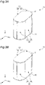
- Fig. 3A is a perspective view illustrating a first capacitor 20 included in a first capacitor group 12 of the capacitor module 1 of Fig. 1 .
- Fig. 3B is a perspective view illustrating a second capacitor 30 included in a second capacitor group 13 of the capacitor module 1 of Fig. 1 .
- Fig. 4 is a perspective view illustrating a first bus bar 14 and a second bus bar 15 included in the capacitor module 1 of Fig. 1 .
- Fig. 5 is a perspective view illustrating a third bus bar 16 included in the capacitor module 1 of Fig. 1 .
- Fig. 6 is a perspective view illustrating an insulating member 18 included in the capacitor module 1 of Fig. 1 .
- Fig. 7 is a cross-sectional view of the capacitor module 1 of Fig. 2 taken along line A-A.
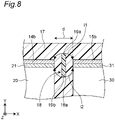
- Fig. 8 is an enlarged view of a part of Fig. 7 .
- Fig. 9 is a cross-sectional view of the capacitor module 1 of Fig. 2 taken along line B-B.
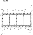
- Fig. 10 is a cross-sectional view of the capacitor module 1 of Fig. 2 taken along line C-C.
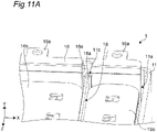
- Fig. 11A is an enlarged perspective view of a part of the capacitor module 1 of Fig. 1 .
- Fig. 11B is a perspective view of the capacitor module 1 of Fig. 11A with the insulating member 18 omitted.
- X, Y, and Z directions in the drawing respectively indicate a lateral direction, a height direction, and a longitudinal direction of the capacitor module 1.
- the capacitor module 1 includes a case 11, the first capacitor group 12, the second capacitor group 13, the first bus bar 14, the second bus bar 15, the third bus bar 16, a sealing resin 17, and the insulating member 18.
- the sealing resin 17 is not illustrated.
- the case 11 has an opening 11a (see Fig. 1 ) provided at a position opposing a bottom surface 11b (see Fig. 7 ).
- the case 11 houses the first capacitor group 12, the second capacitor group 13, the first bus bar 14, the second bus bar 15, the third bus bar 16, and the insulating member 18, and the case 11 is filled with the sealing resin 17.
- each of the first bus bar 14, the second bus bar 15, and the third bus bar 16 is provided to extend to the outside along the side surface of the case 11.
- the first bus bar 14, the second bus bar 15, and the third bus bar 16 respectively have terminals 14a, 15a, and 16a that connect an external element and circuit.
- the first capacitor group 12 is an aggregate of capacitors including a plurality of the first capacitors 20 illustrated in Fig. 3A .
- the second capacitor group 13 is an aggregate of capacitors including one or a plurality of the second capacitors 30 illustrated in Fig. 3B .
- the first capacitor group 12 and the second capacitor group 13 have different functions (for example, capacitance), and therefore the capacitor module 1 has two functions.
- the first capacitor group 12 includes six first capacitors 20, and the second capacitor group 13 includes two second capacitors 30.
- Each of the first capacitor 20 and the second capacitor 30 is a wound type film capacitor.
- the first capacitor 20 has a first electrode 21, a second electrode 22, and a side surface 23 connecting the first electrode 21 and the second electrode 22.
- the second capacitor 30 has a third electrode 31, a fourth electrode 32, and a side surface 33 connecting the third electrode 31 and the fourth electrode 32.
- the first bus bar 14 and the second bus bar 15 are disposed on the opening side of the case 11.
- the opening side of the case 11 indicates a side close to the opening 11a relative to the bottom surface 11b in the case 11.
- the first bus bar 14 is connected to the first electrode 21 of each of the first capacitors 20.
- the second bus bar 15 is connected to the third electrode 31 of each of the second capacitors 30.
- the third bus bar 16 having a plate shape is disposed on the bottom surface side of the case 11.
- the bottom surface side of the case 11 indicates a side close to the bottom surface 11b relative to the opening 11a in the case 11.
- Each of the first capacitors 20 and second capacitors 30 are disposed on the third bus bar 16.
- the second electrode 22 of each of the first capacitors 20 and the fourth electrode 32 of each of the second capacitors 30 are connected to the third bus bar 16. That is, each of the first capacitors 20 is disposed such that the first electrode 21 faces the opening side and the second electrode 22 faces the bottom surface side.
- each of the second capacitors 30 is disposed such that the third electrode 31 faces the opening side and the fourth electrode 32 faces the bottom surface side.
- the insulating member 18 is disposed between the first bus bar 14 and the second bus bar 15.
- the insulating member 18 insulates the first electrode 21 of the first capacitor 20 and the first bus bar 14 from the third electrode 31 of the second capacitor 30 and the second bus bar 15.
- the first capacitor 20 is a wound type film capacitor.
- the first capacitor 20 is formed by winding a dielectric film having a metal evaporated film formed on the surface and pressing the wound body of the dielectric film into a flat shape. Therefore, as illustrated in Fig. 2A, the side surface 23 of the first capacitor 20 has a pair of flat portions 24 opposing each other and a pair of curved portions 25 connecting the pair of flat portions 24.
- the dielectric film of the first capacitor 20 for example, a plastic film such as polyethylene terephthalate, polypropylene, polyphenylene sulfide, or polyethylene naphthalate can be used.
- a plastic film such as polyethylene terephthalate, polypropylene, polyphenylene sulfide, or polyethylene naphthalate
- the metal evaporated film formed on the surface of the plastic film Al, Zn, or the like can be used.
- the first electrode 21 and the second electrode 22 are formed by spraying Zn or the like, for example, onto the end portion of the wound dielectric film.
- the first bus bar 14 is a conductive member connected to the first electrode 21 of each of the first capacitors 20 of the first capacitor group 12. As illustrated in Fig. 4 , the first bus bar 14 has the terminal 14a connected to an element, a circuit, or the like outside the capacitor module 1, and an electrode contact portion 14b in contact with each of the first electrodes 21.
- the terminal 14a and the electrode contact portion 14b are integrally formed by bending one metal plate.
- the first bus bar 14 is formed of a conductive metal such as Al, Cu, or brass.
- the electrode contact portion 14b is formed with a hole 14c for connecting each of the first electrodes 21 by solder.
- the terminal 14a is formed by extending in the height direction (Y direction) from the electrode contact portion 14b and being bent in the longitudinal direction (Z direction) near the opening 11a of the case 11.
- the second bus bar 15 is a conductive member connected to the third electrode 31 of each of the second capacitors 30 of the second capacitor group 13. As illustrated in Fig. 4 , the second bus bar 15 has the terminal 15a connected to an element, a circuit, or the like outside the capacitor module 1, and an electrode contact portion 15b in contact with each of the third electrodes 31.
- the terminal 15a and the electrode contact portion 15b are integrally formed by bending one metal plate.
- the second bus bar 15 is formed of a conductive metal such as Al, Cu, or brass.
- the electrode contact portion 15b is provided with a hole 15c for connecting each of the third electrodes 31 by solder.
- the terminal 15a is formed by extending in the height direction (Y direction) from the electrode contact portion 15b and being bent in the longitudinal direction (Z direction) near the opening 11a of the case 11.
- the first bus bar 14 and the second bus bar 15 are arranged at an interval d in the lateral direction (X direction) in order to be electrically insulated as illustrated in Fig. 8 described later.
- the third bus bar 16 is connected to the second electrode 22 of each of the first capacitors 20 of the first capacitor group 12 and the fourth electrode 32 of each of the second capacitors 30 of the second capacitor group 13. As illustrated in Fig. 5 , the third bus bar 16 has a terminal 16a, an electrode contact portion 16b, and an extending portion 16c.
- the terminal 16a is connected to an element or a circuit outside the capacitor module 1.
- the electrode contact portion 16b is commonly in contact with the second electrode 22 and the fourth electrode 32.
- the extending portion 16c extends outward from the electrode contact portion 16b along the side surface of the case 11.
- the terminal 16a, the electrode contact portion 16b, and the extending portion 16c are integrally formed by bending one metal.
- the third bus bar 16 is formed of a conductive metal such as Al, Cu, or brass.
- the electrode contact portion 16b is provided with a hole 16d for connecting each of the second electrodes 22 and fourth electrodes 32 by solder.
- the extending portion 16c extends in the height direction (Y direction) from the electrode contact portion 16b, and is bent in the longitudinal direction (Z direction) near the opening 11a of the case 11.
- the extending portion 16c of the third bus bar is provided with a through hole 16e.
- the through hole 16e is for inserting the insulating member 18 in the -Y direction.
- the insulating member 18 is a member that insulates between the first bus bar 14 and the first electrode 21 and the second bus bar 15 and the third electrode 31. By disposing the insulating member 18, it is possible to more reliably insulate the first bus bar 14 and the first electrode 21 and the second bus bar 15 and the third electrode 31.
- the insulating member 18 has a first portion 18a having a plate shape and a second portion 18b extending so as to intersect along the first portion 18a.
- the insulating member 18 is formed of an electrically insulating resin such as polyphenylene sulfide (PPS resin) or polybutylene terephthalate (PBT resin).
- PPS resin polyphenylene sulfide
- PBT resin polybutylene terephthalate
- the insulating member 18 is formed by injection molding, and therefore a resin suitable for injection molding is preferably used.
- the first portion 18a of the insulating member 18 is disposed along between the electrode contact portion 14b of the first bus bar 14 and the electrode contact portion 15b of the second bus bar 15.
- the first portion 18a has one end portion 19a positioned on the opening side relative to the electrode contact portion 14b of the first bus bar 14 and the electrode contact portion 15b of the second bus bar 15 in the direction from the opening 11a toward the bottom surface 11b, that is, in the height direction (Y direction) as illustrated in Figs. 7 and 8 .
- An other end portion 19b of the second portion 18b is positioned on the bottom surface side relative to the first electrode 21 and the third electrode 31.
- arrows i1 and i2 illustrated in Fig. 8 indicate the insulation distances i1 and i2 between the first bus bar 14 and the first electrode 21 and the second bus bar 15 and the third electrode 31.
- the interval d between the first bus bar 14 and the second bus bar 15 becomes the insulation distance, and thus the interval d needs to be increased, which makes it difficult to downsize the capacitor module 1.
- the insulating member 18 As in the present embodiment, it is possible to secure the insulation distance while reducing the interval d between the first bus bar 14 and the second bus bar 15. Therefore, it is possible to more reliably insulate between the first bus bar 14 and the first electrode 21 and the second bus bar 15 and the third electrode 31.
- the insulation distances i1 and i2 are preferably set to appropriate values in consideration of the maximum applied voltages of the capacitor groups 12 and 13. It is possible to change the insulation distance by adjusting the positions in the height direction of the one end portion 19a and the other end portion 19b of the first portion 18a of the insulating member 18.
- the second portion 18b of the insulating member 18 is positioned on the bottom surface side of the case 11 with respect to a surface 14d on the first electrode 21 side of the electrode contact portion 14b of the first bus bar 14 and a surface 15d on the third electrode 31 side of the electrode contact portion 15b of the second bus bar 15. That is, the second portion 18b of the insulating member 18 is disposed on the lower side in the height direction of the first bus bar 14 and the second bus bar 15. Since the second portion 18b is disposed on the lower side of the first bus bar 14 and the second bus bar 15, it is possible to prevent the insulating member 18 from uplifting due to the buoyancy of the sealing resin 17.
- the second portion 18b of the insulating member 18 is disposed between the adjacent curved portions 25 of the adjacent first capacitors 20 and between the adjacent curved portions 35 of the adjacent second capacitors 30. Since the first capacitor 20 has a shape having the curved portion 25, a space is generated between the adjacent curved portions 25 of the adjacent first capacitors 20. Similarly, in the case of the second capacitor 30, a space is generated between the adjacent curved portions 35. When the second portion 18b of the insulating member 18 is disposed using this space, the second portion 18b of the insulating member 18 can be disposed without enlarging the case 11, and the uplift of the insulating member 18 can be prevented while effectively using the space.
- the first portion 18a of the insulating member 18 is provided with a third portion 18c that prevents positional displacement in a horizontal direction including the lateral direction (X direction) and the longitudinal direction (Z direction).
- the electrode contact portion 14b of the first bus bar 14 and the electrode contact portion 15b of the second bus bar 15 are provided with cutouts 14e and 15e, respectively.
- the third portion 18c is disposed so as to be placed on a part of the first electrode 21 and a part of the third electrode 31.
- the third portion 18c of the insulating member 18 is disposed on the upper side in the height direction of the first capacitor 20 and the second capacitor 30 and is surrounded by the cutouts 14e and 15e, so that the insulating member 18 can be prevented from being displaced in the longitudinal direction (Z direction) or the lateral direction (Z direction).
- the movement in the +Y direction can be restricted by the second portion 18b, and the movement in the X direction and the Z direction can be restricted by the third portion 18c.
- the case 11 houses each component of the capacitor module 1.
- the case 11 has the opening 11a provided at a position opposing the bottom surface 11b.
- the case 11 has the opening 11a and the bottom surface 11b that have a substantially square shape, and has a box shape.
- the shape of the case 11 is not limited to this, and can take various shapes depending on the arrangement of the capacitor group.
- the case 11 is formed of, for example, a synthetic resin such as polyphenylene sulfide (PPS resin) or polybutylene terephthalate (PBT resin).
- a protrusion 11c for positioning the insulating member 18 is provided in the case 11.
- the protrusion 11c is a protrusion provided inward from the inner side surface of the case 11, and provides a recess 11d that receives the first portion 18a of the insulating member 18 in a direction from the opening 11a toward the bottom surface 11b.
- the protrusion 11c restricts the movement of the insulating member 18 in the lateral direction (X direction) and the longitudinal direction (Z direction). That is, the insulating member 18 is positioned in the X direction and the Z direction by the protrusion 11c.
- the shape of the protrusion 11c is not limited to that illustrated in Figs. 11A and 11B , and is only required to be a shape as long as it can hold the end portion of the insulating member 18.
- the movement of the insulating member 18 in the X direction and the Z direction is restricted. Furthermore, the movement of the insulating member 18 in the -Y direction is also restricted. Since the periphery of the insulating member 18 is filled with the sealing resin 17, the insulating member 18 is positioned by the protrusion 11c of the case 11 and the sealing resin 17.
- the through hole 16e of the third bus bar 16 overlaps the protrusion 11c of the case 11.
- the bottom surface 11b of the case 11 is flat.
- the sealing resin 17 easily spreads over the entire the bottom surface 11b as compared with a case where the bottom surface 11b is provided with a convex, and therefore the filling property of the sealing resin 17 can be improved.
- the sealing resin 17 is filled in the case 11 to seal each component of the capacitor module 1.
- the sealing resin 17 is a thermosetting resin, and for example, an epoxy resin can be used. Alternatively, it may be a urethane resin.
- FIGS. 12A to 12F are views illustrating the manufacturing process of the capacitor module 1 according to the first embodiment.
- the third bus bar 16 is prepared. As illustrated in Fig. 5 , the third bus bar 16 can be formed by pressing a metal plate, for example. In order to insulate between the third bus bar 16 and the first electrode 21 of each of the first capacitors 20 and the third electrode 31 of each of the second capacitors 30, an insulating paper 41 is attached to the extending portion 16c of the third bus bar 16.
- each of the first capacitors 20 and second capacitors 30 is disposed in the electrode contact portion 16b of the third bus bar 16. Specifically, as illustrated in Fig. 12A , each of the first capacitors 20 and second capacitors 30 is disposed such that the second electrode 22 and the fourth electrode 32 face the electrode contact portion 16b.
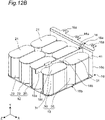
- the insulating member 18 is disposed. Specifically, as illustrated in Fig. 12B , the first portion 18a of the insulating member 18 is disposed between the first capacitor group 12 and the second capacitor group 13. At this time, the second portion 18b is positioned between the curved portions 25 of the first capacitors 20 and between the curved portions 35 of the second capacitors 30. The third portion 18c is placed on the first capacitor 20 and the second capacitor 30.
- the first portion 18a of the insulating member 18 is disposed so as to be held between the first capacitor group 12 and the second capacitor group 13, and the movement in the lateral direction is restricted. At this time, the end portion of the first portion 18a passes through the through hole 16e of the third bus bar, and therefore the first portion 18a and the third bus bar 16 do not interfere with each other.
- the insulating member 18 is not in a fixed state, and is disposed so that the end portion of the insulating member 18 can be fitted into the recess 11d in the process of inserting each component described later into the case 11.
- the insulating member 18 becomes in a state of being movable in the Y direction by the second portion 18b being positioned in the -Y direction relative to the first electrode 21 and the third electrode 31, and therefore it is possible to easily perform fitting to the recess 11d.
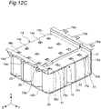
- the first bus bar 14 and the second bus bar 15 are disposed. Specifically, as illustrated in Fig. 12C , the electrode contact portion 14b of the first bus bar 14 is placed on the first electrode 21 of each of the first capacitors 20 of the first capacitor group 12. The electrode contact portion 15b of the second bus bar 15 is placed on the third electrode 31 of each of the second capacitors 30 of the second capacitor group 13. At this time, the first bus bar 14 and the second bus bar 15 are disposed such that third portion 18c of the insulating member 18 is positioned in the cutouts 14e and 15e of the first bus bar 14 and the second bus bar 15, respectively.
- the electrode contact portion 14b and each of the first electrodes 21 are connected by solder (not illustrated).
- the electrode contact portion 15b and each of the third electrodes 31 are connected by solder (not illustrated).
- the third bus bar 16 is connected to each of the second electrodes 22 and fourth electrodes 32 by solder (not illustrated). Specifically, as illustrated in Fig. 12D , the third bus bar 16 is electrically connected to the second electrode 22 and the fourth electrode 32 by soldering in the hole 16d provided in the electrode contact portion 16b of the third bus bar 16.
- each of the first capacitors 20 and second capacitors 30, the first bus bar 14, the second bus bar 15, the third bus bar 16, and the insulating member 18 that have been soldered are inserted into the case 11.
- the end portion of the first portion 18a of the insulating member 18 is inserted into recess 11d of the protrusion 11c of the case 11 (see Fig. 11A ).
- the insulating member 18 is positioned in the X direction and the Z direction inside the case 11.
- the case 11 After insertion into the case 11, as illustrated in Fig. 12F , the case 11 is filled with the sealing resin 17, and the sealing resin 17 is cured to complete the capacitor module 1. At this time, the movement of the second portion 18b of the insulating member 18 in the +Y direction is restricted by the first bus bar 14 and the second bus bar 15 (see Fig. 9 ). Therefore, it is possible to prevent uplift of the insulating member 18 when the sealing resin 17 is filled. Since the bottom surface 11b of the case 11 is formed flat, the filling property of the sealing resin 17 is improved.
- capacitor module 1 According to the capacitor module 1 according to the first embodiment, it is possible to achieve the following effects.
- the capacitor module 1 includes the case 11, the first capacitor group 12, the second capacitor group 13, the first bus bar 14, the second bus bar 15, the third bus bar 16, the sealing resin 17, and the insulating member 18.
- the case 11 has the opening 11a provided at a position opposing the bottom surface 11b.
- the first capacitor group 12 includes one or a plurality of the first capacitors 20.
- the first capacitor 20 is disposed inside the case 11 and has the first electrode 21, the second electrode 22, and the side surface 23 connecting the first electrode 21 and the second electrode 22.
- the second capacitor group 13 includes one or a plurality of the second capacitors 30.
- the second capacitor 30 is disposed inside the case 11, and includes the third electrode 31, the fourth electrode 32, and the side surface 33 connecting third electrode 31 and the fourth electrode 32.
- the first bus bar 14 is disposed on the opening 11a side with respect to the first capacitor group 12 inside the case 11, and has a plate shape having the electrode contact portion 14b in contact with the first electrode 21.
- the second bus bar 15 is disposed on the opening 11a side with respect to the second capacitor group 13 inside the case 11, and has a plate shape having the electrode contact portion 15b in contact with the third electrode 31.
- the third bus bar 16 is disposed on the bottom surface 11b side with respect to the first capacitor group 12 and the second capacitor group 13 inside the case 11, and has the electrode contact portion 16b commonly in contact with the second electrode 22 and the fourth electrode 32.
- the sealing resin 17 is filled in the case 11.
- the insulating member 18 is provided between the electrode contact portion 14b of the first bus bar 14 and the electrode contact portion 15b of the second bus bar 15, and is surrounded by the sealing resin 17.
- the insulating member 18 By providing the insulating member 18, it is possible to improve insulation between the first bus bar 14 and the first electrode 21 and the second bus bar 15 and the third electrode 31 as compared with a case where the insulating member 18 is not disposed and only the sealing resin 17 is provided. When the insulating member 18 is not disposed, insulation is provided by the sealing resin 17, but there is a risk of insulation failure due to bubbles generated in the sealing resin 17. By providing the insulating member 18 separately from the sealing resin 17, it is possible to reliably insulate between the first bus bar 14 and the first electrode 21 and the second bus bar 15 and the third electrode 31, and the insulation is improved.
- the insulating member 18 By disposing the insulating member 18, it is possible to secure the long insulation distances i1 and i2 while reducing the distance d between the first bus bar 14 and the first electrode 21 and the second bus bar 15 and the third electrode 31. Therefore, it is possible to reduce the interval d between the first bus bar 14 and the first electrode 21 and the second bus bar 15 and the third electrode 31, thereby contributing to downsizing of the capacitor module 1.
- the one end portion 19a of the insulating member 18 is positioned on the opening side of the case 11 relative to the electrode contact portion 14b of the first bus bar 14 and the electrode contact portion 15b of the second bus bar 15 in the direction from the opening 11a toward the bottom surface 11b.
- the other end portion 19b of the insulating member 18 is positioned on the bottom surface side of the case 11 relative to the first electrode 21 and the third electrode 31.
- the insulation distance between the first bus bar 14 and the second bus bar 15 can be changed by the positions in the height direction (Y direction) of the end portions 19a and 19b of the insulating member 18. Referring to Fig. 8 , if the position in the height direction of the one end portion 19a is positioned upper (+Y direction) than that in Fig. 8 , the insulation distance i1 becomes longer. Similarly, if the position in the height direction of the other end portion 19b of the insulating member 18 is positioned lower (-Y direction) than that in Fig. 8 , the insulation distance i2 becomes longer.
- the lengths of the insulation distances i1 and i2 are preferably set appropriately according to the capacitance of the capacitor module 1 or the like.
- the insulation distance is the distance d between the electrode contact portion 14b and the electrode contact portion 15b. In this case, in order to secure an appropriate insulation distance, the distance d is increased, which makes it difficult to downsize the capacitor module 1.
- the insulation distance is the distance d between the first electrode 21 and the third electrode 31. Also in this case, in order to secure an appropriate insulation distance, the distance d is increased.
- the inner side surface of the case 11 has the recess 11d that receives the insulating member 18 in the direction from the opening 11a toward the bottom surface 11b, and is provided with the protrusion 11c that positions the insulating member 18.
- Such configuration makes it possible to prevent positional displacement of the insulating member 18 in the case 11, and provide insulation more reliably.
- the third bus bar 16 further has the extending portion 16c extending to the outside of the case 11 through the opening 11a along the side surface of the case 11 from the electrode contact portion 16b of the third bus bar 16.
- the extending portion 16c is provided with the through hole 16e through which the insulating member 18 passes. Such configuration makes it possible to prevent interference between the third bus bar 16 and the insulating member 18.
- the insulating member 18 includes the first portion 18a and the second portion 18b.
- the first portion 18a extends along between the electrode contact portion 14b of the first bus bar 14 and the electrode contact portion 15b of the second bus bar 15.
- the second portion 18b extends so as to intersect the first portion 18a, and extends so as to be positioned on the bottom surface side of the case 11 with respect to the surface 14d on the first electrode 21 side of the electrode contact portion 14b of the first bus bar 14 and the surface 15d on the third electrode 31 side of the electrode contact portion 15b of the second bus bar 15.
- Such configuration makes it possible to prevent uplift due to buoyancy of the sealing resin 17 of the insulating member 18.
- the side surface 23 of the first capacitor 20 has a pair of flat portions 24 opposing each other and a pair of curved portions 25 connecting the pair of flat portions 24.
- the side surface 33 of the second capacitor 30 includes a pair of flat portions 34 and a pair of the curved portions 35 connecting the pair of flat portions 34.
- the second portion 18b of the insulating member 18 is disposed between the adjacent curved portions 25 of the adjacent first capacitors 20 and between the adjacent curved portions 35 of the adjacent second capacitors 30. Such configuration makes it possible to dispose the second portion 18b in a space provided between the adjacent curved portions 25 and between the adjacent curved portions 35, thereby contributing to downsizing of the capacitor module 1.
- the bottom surface 11b of the case 11 is flat. Such configuration makes it possible to improve the filling property of the sealing resin 17.
- the fluidity of the resin is improved, and therefore it is possible to prevent the manufacturing cost from increasing due to time taken for filling of the resin due to blocking of the flow of the resin when filling the case with the resin.
- manufacturing of the case 11 becomes easy, and therefore downsizing can be achieved, which contributes to downsizing of the capacitor module 1.
- the first capacitor group 12 includes the six first capacitors 20 and the second capacitor group 13 includes the two second capacitors 30 has been described, but the present invention is not limited to this.
- the numbers of capacitors included in the first capacitor group 12 and the second capacitor group 13 are only required to be one or more.
- the present invention is not limited to this.
- the second portion 18b is only required to extend to either the first capacitor group 12 side or the second capacitor group 13 side. Two or more second portions 18b may be provided.
- the insulating member 18 is provided with the second portion 18b and the third portion 18c has been described, but the second portion 18b and the third portion 18c need not be provided.
- the insulating member 18 is not provided with the third portion 18c, the respective cutouts 14e and 15e of the first bus bar 14 and the second bus bar 15 need not be provided.
- Fig. 13A is an enlarged perspective view of a part of a capacitor module 1a according to a modification of the first embodiment of the present invention.
- Fig. 13B is a perspective view of the capacitor module 1a of Fig. 13A with the insulating member 18 omitted.
- the sealing resin 17 is omitted.
- the case 11 is not provided with a protrusion, and the insulating member 18 is positioned by being received by the third bus bar 16 at one end on the bottom surface side of a through hole 16f provided in the extending portion 16c.
- the through hole 16f is provided with a portion whose width decreases from the opening side toward the bottom surface side and a portion having substantially the same constant width as that of the insulating member 18.
- the insulating member 18 is positioned by the portion having the constant width. Therefore, when the insulating member 18 is inserted from the opening side to the bottom surface side, the insulating member 18 is positioned in the lateral direction (X direction).
- the insulating member 18 can be positioned with a simple configuration and the manufacturing cost can be reduced.
- the insulating member 18 is already positioned in the state of Fig. 12B . Therefore, it is possible to prevent positional displacement of the insulating member 18 with respect to the bus bar or the capacitor when inserting the insulating member 18 into the case 11 as in Fig. 12E . Therefore, the positioning accuracy of the insulating member 18 is improved, and the insulation can be improved.
- a capacitor module 1b according to the second embodiment of the present invention will be described.
- Fig. 14 is a perspective view of the capacitor module 1b according to the second embodiment with a case and a sealing resin omitted.
- Fig. 15 is an enlarged view of the region R1 of the capacitor module 1b of Fig. 14 .
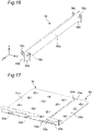
- Fig. 16 is a view illustrating an insulating member 58 of the capacitor module 1b of Fig. 14 .
- Fig. 17 is a view illustrating a first bus bar 54 and a second bus bar 55 of the capacitor module 1b of Fig. 14 .
- the second embodiment is different from the first embodiment in a point that a second portion 58b of the insulating member 58 has a protrusion 58c, and the protrusion 58c is inserted into holes 54e and 55e (see Fig. 17 ) provided in the first bus bar 54 and the second bus bar 55, respectively.
- the insulating member 58 has two second portions 58b at each of both ends of a first portion 58a. That is, four second portions 58b are provided in the first portion 58a.
- the protrusion 58c is provided from each second portion 58b of the insulating member 58 toward the +Y direction. The tip end of the protrusion 58c is provided in a hook shape.
- the first bus bar 54 and the second bus bar 55 are provided with the holes 54e and 55e, respectively. Since each protrusion 58c of the second portion 58b of the insulating member 58 is inserted into the hole 54e of the first bus bar 54 or the hole 55e of the second bus bar 55, a hook of the protrusion 58c is caught and fixed to the hole 54e or 55e. That is, each of the protrusion 58c and the hole 54e or 55e is fitted by snap-fitting. In this manner, the insulating member 58 is joined to the first bus bar 54 and the second bus bar 55.
- the insulating member 58 is joined and positioned with the first bus bar 54 and the second bus bar 55. Therefore, a protrusion or a through hole for positioning the insulating member 58 is not provided in the case 11 and the third bus bar 16. Since the insulating member 18 is fitted to the first bus bar 54 and the second bus bar 55 by snap-fitting, the insulating member 58 is not provided with a portion that prevents uplift (the second portion 18b of the first embodiment), and has a configuration simpler than that of the first embodiment.
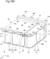
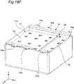
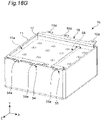
- FIGS. 18A to 18F are views illustrating the manufacturing process of the capacitor module 1b according to the second embodiment.
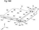
- first bus bar 54 and the second bus bar 55 are prepared as illustrated in Fig. 18A .
- the first bus bar 54 is provided with an electrode contact portion 54b, a terminal 54a, a hole 54c for soldering, and the hole 54e for joining with the insulating member 58.
- the second bus bar 55 is provided with an electrode contact portion 55b, a terminal 55a, a hole 55c for soldering, and the hole 55e for joining with the insulating member 58.
- the protrusion 58c of the insulating member 58 is inserted into the hole 54e of the first bus bar 54 and the hole 55e of the second bus bar 55.
- Each protrusion 58c of the insulating member 58 is inserted in the direction (Y direction) from the bottom surface 11b of the case 11 toward the opening 11a. Since the insulating member 58 is joined to the first bus bar 54 and the second bus bar 55 by snap-fitting, the insulating member 58 can be firmly fixed to the first bus bar 54 and the second bus bar 55.
- each of the first capacitors 20 and second capacitors 30 is disposed in the electrode contact portion 16b of the third bus bar 16.
- the first bus bar 54 and the second bus bar 55 joined to the insulating member 58 in Fig. 18B are disposed in the first capacitor 20 and the second capacitor 30.
- first bus bar 54 and the second bus bar 55 are disposed, the first bus bar 54 and the first electrode 21 of each of the first capacitors 20, and the second bus bar 55 and the third electrode 31 of each of the second capacitors 30 are connected by solder (not illustrated).
- the first bus bar 54 and each of the first electrodes 21 are electrically connected by soldering in the hole 54c provided in the electrode contact portion 54b of the first bus bar 54.
- the second bus bar 55 and the third electrode 31 are also soldered in the hole 55c provided in the electrode contact portion 55b of the second bus bar 55, whereby the second bus bar 55 and the third electrode 31 are electrically connected.
- the third bus bar 16 is connected to each of the second electrodes 22 and fourth electrodes 32 by solder (not illustrated).
- the third bus bar 16 is electrically connected to the second electrode 22 and the fourth electrode 32 by soldering in the hole 16d provided in the electrode contact portion 16b of the third bus bar 16.
- each of the first capacitors 20 and second capacitors 30, the first bus bar 54, the second bus bar 55, the third bus bar 16, and the insulating member 58 that have been soldered are inserted into the case 11. At this time, no protrusion is provided on the case 11, and alignment between the insulating member 58 and the case 11 is unnecessary, and therefore arrangement is easy.
- the case 11 After insertion into the case 11, as illustrated in Fig. 18G , the case 11 is filled with the sealing resin 17, and the sealing resin 17 is cured to complete the capacitor module 1b. At this time, the protrusion 58c of the insulating member 58 is inserted into each of the holes 54e and 55e. Therefore, it is possible to prevent the insulating member 58 from uplifting due to the buoyancy of the sealing resin 17 without separately providing an uplift prevention structure (the second portion 18b of the first embodiment) of the insulating member 58.
- capacitor module 1b According to the capacitor module 1b according to the second embodiment, it is possible to achieve the following effects.
- the second portion 58b of the insulating member 58 of the capacitor module 1b has the protrusion 58c, and is inserted into the holes 54e and 55e provided in first bus bar 54 and the second bus bar 55, respectively.
- a capacitor module 1c according to a modification of the second embodiment will be described with reference to Figs. 19 to 21 .
- Fig. 19 is a perspective view of the capacitor module 1c according to a modification of the second embodiment with the case and the sealing resin omitted.
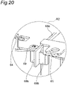
- Fig. 20 is an enlarged view of the region R2 of the capacitor module 1c of Fig. 19 .
- Fig. 21 is a view illustrating a first bus bar 64, a second bus bar 65, and an insulating member 68 of the capacitor module 1c of Fig. 19 .
- the insulating member 58 is joined to the first bus bar 54 and the second bus bar 55 by the snap-fit structure, they are joined by screws in the capacitor module 1c.
- the insulating member 68 is joined to the first bus bar 64 and the second bus bar 65 by four screws 69.
- a second portion 68b of the insulating member 68 has a recess 68c.
- the first bus bar 64 and the second bus bar 65 are provided with circular holes 64e and 65e, respectively.
- the capacitor module 1c further has the screws 69 inserted into the holes 64e and 65e provided in the first bus bar 64 and the second bus bar 65 and the recesses 68c respectively.
- Such configuration makes it possible to more firmly fix the insulating member 68, the first bus bar 64, and the second bus bar 65 as compared with the snap-fitting. It is possible to improve the positioning accuracy of the insulating member 68.
- the present invention is useful for capacitors used in various electronic equipment, electric equipment, industrial equipment, vehicle devices, and the like.
Landscapes
- Engineering & Computer Science (AREA)
- Power Engineering (AREA)
- Microelectronics & Electronic Packaging (AREA)
- Manufacturing & Machinery (AREA)
- Fixed Capacitors And Capacitor Manufacturing Machines (AREA)
Abstract
Description
- The present invention relates to a capacitor module.
- There is known a capacitor module in which one or a plurality of capacitors formed by winding or layering a dielectric film having a metal film on the surface are housed in a case, and bus bars are connected to electrodes at both ends of each capacitor.
- For example,
Patent Document 1 discloses a film capacitor in which a capacitor element and an electronic component are separately housed with a partition plate provided on a bottom surface of a case. - Patent Document 1:
Japanese Laid-Open Patent Publication No. 2001-210548 - The film capacitor described in
JP 2001-210548 A - Therefore, an object of the present invention is to provide a capacitor module with improved insulation.
- A capacitor module according to an aspect of the present invention includes:
- a case with an opening provided at a position opposing a bottom surface;
- a first capacitor group disposed inside the case and including one or a plurality of first capacitors each having a first electrode, a second electrode, and a side surface connecting the first electrode and the second electrode;
- a second capacitor group disposed inside the 'case and including one or a plurality of second capacitors each having a third electrode, a fourth electrode, and a side surface connecting the third electrode and the fourth electrode;
- a first bus bar having a plate shape, the first bus bar being disposed on the opening side with respect to the first capacitor group inside the case and having an electrode contact portion in contact with the first electrode;
- a second bus bar having a plate shape, the second bus bar being disposed on the opening side with respect to the second capacitor group inside the case and having an electrode contact portion in contact with the third electrode;
- a third bus bar disposed on the bottom surface side with respect to the first capacitor group and the second capacitor group inside the case and having an electrode contact portion commonly in contact with the second electrode and the fourth electrode;
- a sealing resin with which the case is filled; and
- an insulating member provided between the electrode contact portion of the first bus bar and the electrode contact portion of the second bus bar and surrounded by the sealing resin.
- According to the present invention, it is possible to provide a capacitor module with improved insulation.
-
-
Fig. 1 is a perspective view schematically illustrating a capacitor module according to a first embodiment of the present invention; -
Fig. 2 is a plan view of the capacitor module ofFig. 1 ; -
Fig. 3A is a perspective view illustrating a first capacitor included in a first capacitor group of the capacitor module ofFig. 1 ; -
Fig. 3B is a perspective view illustrating a second capacitor included in a second capacitor group of the capacitor module ofFig. 1 ; -
Fig. 4 is a perspective view illustrating a first bus bar and a second bus bar included in the capacitor module ofFig. 1 ; -
Fig. 5 is a perspective view illustrating a third bus bar included in the capacitor module ofFig. 1 ; -
Fig. 6 is a perspective view illustrating an insulating member included in the capacitor module ofFig. 1 ; -
Fig. 7 is a cross-sectional view taken along line A-A ofFig. 2 ; -
Fig. 8 is an enlarged view of a part ofFig. 7 ; -
Fig. 9 is a cross-sectional view taken along line B-B ofFig. 2 ; -
Fig. 10 is a cross-sectional view taken along line C-C ofFig. 2 ; -
Fig. 11A is an enlarged perspective view of a part of the capacitor module ofFig. 1 ; -
Fig. 11B is a perspective view of the capacitor module ofFig. 11A with the insulating member omitted; -
Fig. 12A is a view illustrating a manufacturing process of the capacitor module according to the first embodiment; -
Fig. 12B is a view illustrating the manufacturing process of the capacitor module according to the first embodiment; -
Fig. 12C is a view illustrating the manufacturing process of the capacitor module according to the first embodiment; -
Fig. 12D is a view illustrating the manufacturing process of the capacitor module according to the first embodiment; -
Fig. 12E is a view illustrating the manufacturing process of the capacitor module according to the first embodiment; -
Fig. 12F is a view illustrating the manufacturing process of the capacitor module according to the first embodiment; -
Fig. 13A is an enlarged perspective view of a part of the capacitor module according to a modification of the first embodiment of the present invention; -
Fig. 13B is a perspective view of the capacitor module ofFig. 13A with the insulating member omitted; -
Fig. 14 is a perspective view of the capacitor module according to a second embodiment with a case and a sealing resin omitted; -
Fig. 15 is an enlarged view of a region R1 of the capacitor module ofFig. 14 ; -
Fig. 16 is a view illustrating an insulating member of the capacitor module ofFig. 14 ; -
Fig. 17 is a view illustrating a first bus bar and a second bus bar of the capacitor module ofFig. 14 ; -
Fig. 18A is a view illustrating a manufacturing process of the capacitor module according to the second embodiment; -
Fig. 18B is a view illustrating the manufacturing process of the capacitor module according to the second embodiment; -
Fig. 18C is a view illustrating the manufacturing process of the capacitor module according to the second embodiment; -
Fig. 18D is a view illustrating the manufacturing process of the capacitor module according to the second embodiment; -
Fig. 18E is a view illustrating the manufacturing process of the capacitor module according to the second embodiment; -
Fig. 18F is a view illustrating the manufacturing process of the capacitor module according to the second embodiment; -
Fig. 18G is a view illustrating the manufacturing process of the capacitor module according to the second embodiment; -
Fig. 19 is a perspective view of the capacitor module according to a modification of the second embodiment with the case and the sealing resin omitted; -
Fig. 20 is an enlarged view of a region R2 of the capacitor module ofFig. 19 ; and -
Fig. 21 is a view illustrating a first bus bar, a second bus bar, and an insulating member of the capacitor module ofFig. 19 . - A capacitor module having two or more capacitor groups having different functions is known. For example, there is a capacitor module in which each capacitor group is housed in one case and the case is filled with an insulating resin. Each capacitor group includes one or more capacitors. Each capacitor group is insulated by the insulating resin filled in the case. However, in the case of such configuration, there is a problem that insulation quality is deteriorated due to bubbles generated in the insulating resin.
- Therefore, the present inventors have studied a configuration for improving insulation between capacitor groups in a capacitor module having two or more capacitor groups, and have reached the following invention.
- A capacitor module according to an aspect of the present invention includes:
- a case with an opening provided at a position opposing a bottom surface;
- a first capacitor group disposed inside the case and including one or a plurality of first capacitors each having a first electrode, a second electrode, and a side surface connecting the first electrode and the second electrode;
- a second capacitor group disposed inside the case and including one or a plurality of second capacitors each having a third electrode, a fourth electrode disposed on the bottom surface side, and a side surface connecting the third electrode and the fourth electrode;
- a first bus bar having a plate shape, the first bus bar being disposed on the opening side with respect to the first capacitor group inside the case and having an electrode contact portion in contact with the first electrode;
- a second bus bar having a plate shape, the second bus bar being disposed on the opening side with respect to the second capacitor group inside the case and having an electrode contact portion in contact with the third electrode;
- a third bus bar disposed on the bottom surface side with respect to the first capacitor group and the second capacitor group inside the case and having an electrode contact portion commonly in contact with the second electrode and the fourth electrode;
- a sealing resin with which the case is filled; and
- an insulating member provided between the electrode contact portion of the first bus bar and the electrode contact portion of the second bus bar and surrounded by the sealing resin.
- According to this configuration, it is possible to provide a capacitor module with improved insulation.
- The insulating member may be disposed such that, in a direction from the opening toward the bottom surface, one end portion is positioned on the opening side relative to the electrode contact portion of the first bus bar and the electrode contact portion of the second bus bar, and an other end portion is positioned on the bottom surface side relative to the first electrode and the third electrode.
- According to this configuration, it is possible to secure the insulation distance of each capacitor group while reducing the distance between the first capacitor group and the second capacitor group. Therefore, it is possible to achieve downsizing of the capacitor module while improving the insulation.
- A recess that receives the insulating member in a direction from the opening toward the bottom surface may be provided on an inner side surface of the case.
- According to this configuration, it is possible to prevent positional displacement of the insulating member in the case.
- The third bus bar may further have an extending portion extending to an outside of the case through the opening along a side surface of the case from the electrode contact portion of the third bus bar, and a through hole through which the insulating member passes may be provided in the extending portion.
- According to this configuration, it is possible to prevent interference between the third bus bar and the insulating member.
- The insulating member may be positioned by being received by the third bus bar at one end on the bottom surface side of the through hole.
- According to this configuration, it is not necessary to provide a recess in the case, and therefore it is possible to reduce the manufacturing cost.
- The insulating member may include
- a first portion extending along between the electrode contact portion of the first bus bar and the electrode contact portion of the second bus bar, and
- a second portion extending so as to intersect with respect to the first portion and extending so as to be positioned on the bottom surface side of the case with respect to a surface on the first electrode side of the electrode contact portion of the first bus bar and a surface on the third electrode side of the electrode contact portion of the second bus bar.
- According to this configuration, it is possible to prevent uplift due to buoyancy of the sealing resin of the insulating member.
- The side surface of the first capacitor and the side surface of the second capacitor may each include a pair of flat portions opposing each other and a pair of curved portions connecting the pair of flat portions, and
the second portion of the insulating member may be disposed between the adjacent curved portions of the adjacent first capacitors and between the adjacent curved portions of the adjacent second capacitors. - According to this configuration, it is possible to dispose the second portion in an empty space between the capacitors, which contributes to downsizing of the capacitor module.
- The second portion of the insulating member may have a protrusion, and
the protrusion may be inserted into a hole provided in each of the first bus bar and the second bus bar. - According to this configuration, it is possible to easily position the insulating member.
- The second portion of the insulating member may have a recess, and
the capacitor module may further comprise a screw inserted into a hole provided in each of the first bus bar and the second bus bar and the recess. - According to this configuration, it is possible to easily position the insulating member.
- The bottom surface of the case may be flat.
- According to this configuration, it is possible to improve the filling property of the sealing resin.
- The first embodiment according to the present invention will be described below with reference to the accompanying drawings. In each drawing, each element is exaggerated in order to facilitate the description.
-
Fig. 1 is a perspective view schematically illustrating acapacitor module 1 according to the first embodiment of the present invention.Fig. 2 is a plan view of thecapacitor module 1 ofFig. 1 .Fig. 3A is a perspective view illustrating afirst capacitor 20 included in afirst capacitor group 12 of thecapacitor module 1 ofFig. 1 .Fig. 3B is a perspective view illustrating asecond capacitor 30 included in asecond capacitor group 13 of thecapacitor module 1 ofFig. 1 .Fig. 4 is a perspective view illustrating afirst bus bar 14 and asecond bus bar 15 included in thecapacitor module 1 ofFig. 1 .Fig. 5 is a perspective view illustrating athird bus bar 16 included in thecapacitor module 1 ofFig. 1 .Fig. 6 is a perspective view illustrating an insulatingmember 18 included in thecapacitor module 1 ofFig. 1 .Fig. 7 is a cross-sectional view of thecapacitor module 1 ofFig. 2 taken along line A-A.Fig. 8 is an enlarged view of a part ofFig. 7 .Fig. 9 is a cross-sectional view of thecapacitor module 1 ofFig. 2 taken along line B-B.Fig. 10 is a cross-sectional view of thecapacitor module 1 ofFig. 2 taken along line C-C.Fig. 11A is an enlarged perspective view of a part of thecapacitor module 1 ofFig. 1 .Fig. 11B is a perspective view of thecapacitor module 1 ofFig. 11A with the insulatingmember 18 omitted. Note that X, Y, and Z directions in the drawing respectively indicate a lateral direction, a height direction, and a longitudinal direction of thecapacitor module 1. - As illustrated in
Figs. 1 and2 , thecapacitor module 1 includes acase 11, thefirst capacitor group 12, thesecond capacitor group 13, thefirst bus bar 14, thesecond bus bar 15, thethird bus bar 16, a sealingresin 17, and the insulatingmember 18. InFig. 2 , the sealingresin 17 is not illustrated. - The
case 11 has anopening 11a (seeFig. 1 ) provided at a position opposing abottom surface 11b (seeFig. 7 ). Thecase 11 houses thefirst capacitor group 12, thesecond capacitor group 13, thefirst bus bar 14, thesecond bus bar 15, thethird bus bar 16, and the insulatingmember 18, and thecase 11 is filled with the sealingresin 17. - In the
capacitor module 1, each of thefirst bus bar 14, thesecond bus bar 15, and thethird bus bar 16 is provided to extend to the outside along the side surface of thecase 11. Thefirst bus bar 14, thesecond bus bar 15, and thethird bus bar 16 respectively haveterminals - The
first capacitor group 12 is an aggregate of capacitors including a plurality of thefirst capacitors 20 illustrated inFig. 3A . Thesecond capacitor group 13 is an aggregate of capacitors including one or a plurality of thesecond capacitors 30 illustrated inFig. 3B . Thefirst capacitor group 12 and thesecond capacitor group 13 have different functions (for example, capacitance), and therefore thecapacitor module 1 has two functions. In the present embodiment, as illustrated inFig. 2 , thefirst capacitor group 12 includes sixfirst capacitors 20, and thesecond capacitor group 13 includes twosecond capacitors 30. - Each of the
first capacitor 20 and thesecond capacitor 30 is a wound type film capacitor. As illustrated inFig. 3A , thefirst capacitor 20 has afirst electrode 21, asecond electrode 22, and aside surface 23 connecting thefirst electrode 21 and thesecond electrode 22. As illustrated inFig. 3B , thesecond capacitor 30 has athird electrode 31, afourth electrode 32, and aside surface 33 connecting thethird electrode 31 and thefourth electrode 32. - Returning to
Fig. 1 , thefirst bus bar 14 and thesecond bus bar 15 are disposed on the opening side of thecase 11. The opening side of thecase 11 indicates a side close to theopening 11a relative to thebottom surface 11b in thecase 11. Thefirst bus bar 14 is connected to thefirst electrode 21 of each of thefirst capacitors 20. Thesecond bus bar 15 is connected to thethird electrode 31 of each of thesecond capacitors 30. - The
third bus bar 16 having a plate shape is disposed on the bottom surface side of thecase 11. The bottom surface side of thecase 11 indicates a side close to thebottom surface 11b relative to theopening 11a in thecase 11. Each of thefirst capacitors 20 andsecond capacitors 30 are disposed on thethird bus bar 16. Thesecond electrode 22 of each of thefirst capacitors 20 and thefourth electrode 32 of each of thesecond capacitors 30 are connected to thethird bus bar 16. That is, each of thefirst capacitors 20 is disposed such that thefirst electrode 21 faces the opening side and thesecond electrode 22 faces the bottom surface side. Similarly, each of thesecond capacitors 30 is disposed such that thethird electrode 31 faces the opening side and thefourth electrode 32 faces the bottom surface side. - The insulating
member 18 is disposed between thefirst bus bar 14 and thesecond bus bar 15. The insulatingmember 18 insulates thefirst electrode 21 of thefirst capacitor 20 and thefirst bus bar 14 from thethird electrode 31 of thesecond capacitor 30 and thesecond bus bar 15. - Each component of the
capacitor module 1 will be described below in detail. - Since the
first capacitor 20 and thesecond capacitor 30 have the same configuration, only thefirst capacitor 20 will be described here. Thefirst capacitor 20 is a wound type film capacitor. Thefirst capacitor 20 is formed by winding a dielectric film having a metal evaporated film formed on the surface and pressing the wound body of the dielectric film into a flat shape. Therefore, as illustrated in Fig. 2A, theside surface 23 of thefirst capacitor 20 has a pair offlat portions 24 opposing each other and a pair ofcurved portions 25 connecting the pair offlat portions 24. - As the dielectric film of the
first capacitor 20, for example, a plastic film such as polyethylene terephthalate, polypropylene, polyphenylene sulfide, or polyethylene naphthalate can be used. As the metal evaporated film formed on the surface of the plastic film, Al, Zn, or the like can be used. Thefirst electrode 21 and thesecond electrode 22 are formed by spraying Zn or the like, for example, onto the end portion of the wound dielectric film. - The
first bus bar 14 is a conductive member connected to thefirst electrode 21 of each of thefirst capacitors 20 of thefirst capacitor group 12. As illustrated inFig. 4 , thefirst bus bar 14 has the terminal 14a connected to an element, a circuit, or the like outside thecapacitor module 1, and anelectrode contact portion 14b in contact with each of thefirst electrodes 21. - The terminal 14a and the
electrode contact portion 14b are integrally formed by bending one metal plate. Thefirst bus bar 14 is formed of a conductive metal such as Al, Cu, or brass. Theelectrode contact portion 14b is formed with ahole 14c for connecting each of thefirst electrodes 21 by solder. The terminal 14a is formed by extending in the height direction (Y direction) from theelectrode contact portion 14b and being bent in the longitudinal direction (Z direction) near theopening 11a of thecase 11. - The
second bus bar 15 is a conductive member connected to thethird electrode 31 of each of thesecond capacitors 30 of thesecond capacitor group 13. As illustrated inFig. 4 , thesecond bus bar 15 has the terminal 15a connected to an element, a circuit, or the like outside thecapacitor module 1, and anelectrode contact portion 15b in contact with each of thethird electrodes 31. - The terminal 15a and the
electrode contact portion 15b are integrally formed by bending one metal plate. Thesecond bus bar 15 is formed of a conductive metal such as Al, Cu, or brass. Theelectrode contact portion 15b is provided with ahole 15c for connecting each of thethird electrodes 31 by solder. The terminal 15a is formed by extending in the height direction (Y direction) from theelectrode contact portion 15b and being bent in the longitudinal direction (Z direction) near theopening 11a of thecase 11. - The
first bus bar 14 and thesecond bus bar 15 are arranged at an interval d in the lateral direction (X direction) in order to be electrically insulated as illustrated inFig. 8 described later. - The
third bus bar 16 is connected to thesecond electrode 22 of each of thefirst capacitors 20 of thefirst capacitor group 12 and thefourth electrode 32 of each of thesecond capacitors 30 of thesecond capacitor group 13. As illustrated inFig. 5 , thethird bus bar 16 has a terminal 16a, anelectrode contact portion 16b, and an extendingportion 16c. The terminal 16a is connected to an element or a circuit outside thecapacitor module 1. Theelectrode contact portion 16b is commonly in contact with thesecond electrode 22 and thefourth electrode 32. The extendingportion 16c extends outward from theelectrode contact portion 16b along the side surface of thecase 11. - The terminal 16a, the
electrode contact portion 16b, and the extendingportion 16c are integrally formed by bending one metal. Thethird bus bar 16 is formed of a conductive metal such as Al, Cu, or brass. Theelectrode contact portion 16b is provided with ahole 16d for connecting each of thesecond electrodes 22 andfourth electrodes 32 by solder. The extendingportion 16c extends in the height direction (Y direction) from theelectrode contact portion 16b, and is bent in the longitudinal direction (Z direction) near theopening 11a of thecase 11. - As illustrated in
Fig. 5 , the extendingportion 16c of the third bus bar is provided with a throughhole 16e. The throughhole 16e is for inserting the insulatingmember 18 in the -Y direction. - As illustrated in
Figs. 1 and2 , the insulatingmember 18 is a member that insulates between thefirst bus bar 14 and thefirst electrode 21 and thesecond bus bar 15 and thethird electrode 31. By disposing the insulatingmember 18, it is possible to more reliably insulate thefirst bus bar 14 and thefirst electrode 21 and thesecond bus bar 15 and thethird electrode 31. - As illustrated in
Fig. 6 , the insulatingmember 18 has afirst portion 18a having a plate shape and asecond portion 18b extending so as to intersect along thefirst portion 18a. The insulatingmember 18 is formed of an electrically insulating resin such as polyphenylene sulfide (PPS resin) or polybutylene terephthalate (PBT resin). The insulatingmember 18 is formed by injection molding, and therefore a resin suitable for injection molding is preferably used. - As illustrated in
Figs. 1 and2 , thefirst portion 18a of the insulatingmember 18 is disposed along between theelectrode contact portion 14b of thefirst bus bar 14 and theelectrode contact portion 15b of thesecond bus bar 15. Thefirst portion 18a has oneend portion 19a positioned on the opening side relative to theelectrode contact portion 14b of thefirst bus bar 14 and theelectrode contact portion 15b of thesecond bus bar 15 in the direction from theopening 11a toward thebottom surface 11b, that is, in the height direction (Y direction) as illustrated inFigs. 7 and8 . Another end portion 19b of thesecond portion 18b is positioned on the bottom surface side relative to thefirst electrode 21 and thethird electrode 31. - By disposing the
first portion 18a of the insulatingmember 18 in this manner, it is possible to secure insulation distances i1 and i2 between the respective bus bars while reducing the distance between thefirst bus bar 14 and thesecond bus bar 15 as compared with the case of not disposing the insulatingmember 18. In the present embodiment, arrows i1 and i2 illustrated inFig. 8 indicate the insulation distances i1 and i2 between thefirst bus bar 14 and thefirst electrode 21 and thesecond bus bar 15 and thethird electrode 31. - In the case of not disposing the insulating
member 18, the interval d between thefirst bus bar 14 and thesecond bus bar 15 becomes the insulation distance, and thus the interval d needs to be increased, which makes it difficult to downsize thecapacitor module 1. By disposing the insulatingmember 18 as in the present embodiment, it is possible to secure the insulation distance while reducing the interval d between thefirst bus bar 14 and thesecond bus bar 15. Therefore, it is possible to more reliably insulate between thefirst bus bar 14 and thefirst electrode 21 and thesecond bus bar 15 and thethird electrode 31. - The insulation distances i1 and i2 are preferably set to appropriate values in consideration of the maximum applied voltages of the
capacitor groups end portion 19a and theother end portion 19b of thefirst portion 18a of the insulatingmember 18. - As illustrated in
Fig. 9 , thesecond portion 18b of the insulatingmember 18 is positioned on the bottom surface side of thecase 11 with respect to asurface 14d on thefirst electrode 21 side of theelectrode contact portion 14b of thefirst bus bar 14 and asurface 15d on thethird electrode 31 side of theelectrode contact portion 15b of thesecond bus bar 15. That is, thesecond portion 18b of the insulatingmember 18 is disposed on the lower side in the height direction of thefirst bus bar 14 and thesecond bus bar 15. Since thesecond portion 18b is disposed on the lower side of thefirst bus bar 14 and thesecond bus bar 15, it is possible to prevent the insulatingmember 18 from uplifting due to the buoyancy of the sealingresin 17. - Returning to
Fig. 2 , thesecond portion 18b of the insulatingmember 18 is disposed between the adjacentcurved portions 25 of the adjacentfirst capacitors 20 and between the adjacentcurved portions 35 of the adjacentsecond capacitors 30. Since thefirst capacitor 20 has a shape having thecurved portion 25, a space is generated between the adjacentcurved portions 25 of the adjacentfirst capacitors 20. Similarly, in the case of thesecond capacitor 30, a space is generated between the adjacentcurved portions 35. When thesecond portion 18b of the insulatingmember 18 is disposed using this space, thesecond portion 18b of the insulatingmember 18 can be disposed without enlarging thecase 11, and the uplift of the insulatingmember 18 can be prevented while effectively using the space. - In the present embodiment, the
first portion 18a of the insulatingmember 18 is provided with athird portion 18c that prevents positional displacement in a horizontal direction including the lateral direction (X direction) and the longitudinal direction (Z direction). In order to create a space for disposing thethird portion 18c, theelectrode contact portion 14b of thefirst bus bar 14 and theelectrode contact portion 15b of thesecond bus bar 15 are provided withcutouts Fig. 10 , thethird portion 18c is disposed so as to be placed on a part of thefirst electrode 21 and a part of thethird electrode 31. Thethird portion 18c of the insulatingmember 18 is disposed on the upper side in the height direction of thefirst capacitor 20 and thesecond capacitor 30 and is surrounded by thecutouts member 18 can be prevented from being displaced in the longitudinal direction (Z direction) or the lateral direction (Z direction). - As described above, in the insulating
member 18, the movement in the +Y direction can be restricted by thesecond portion 18b, and the movement in the X direction and the Z direction can be restricted by thethird portion 18c. - The
case 11 houses each component of thecapacitor module 1. In the present embodiment, thecase 11 has theopening 11a provided at a position opposing thebottom surface 11b. In the present embodiment, thecase 11 has theopening 11a and thebottom surface 11b that have a substantially square shape, and has a box shape. The shape of thecase 11 is not limited to this, and can take various shapes depending on the arrangement of the capacitor group. Thecase 11 is formed of, for example, a synthetic resin such as polyphenylene sulfide (PPS resin) or polybutylene terephthalate (PBT resin). - As illustrated in
Figs. 11A and11B , aprotrusion 11c for positioning the insulatingmember 18 is provided in thecase 11. Theprotrusion 11c is a protrusion provided inward from the inner side surface of thecase 11, and provides arecess 11d that receives thefirst portion 18a of the insulatingmember 18 in a direction from theopening 11a toward thebottom surface 11b. Theprotrusion 11c restricts the movement of the insulatingmember 18 in the lateral direction (X direction) and the longitudinal direction (Z direction). That is, the insulatingmember 18 is positioned in the X direction and the Z direction by theprotrusion 11c. The shape of theprotrusion 11c is not limited to that illustrated inFigs. 11A and11B , and is only required to be a shape as long as it can hold the end portion of the insulatingmember 18. - When the
first portion 18a of the insulatingmember 18 is disposed on theprotrusion 11c, the movement of the insulatingmember 18 in the X direction and the Z direction is restricted. Furthermore, the movement of the insulatingmember 18 in the -Y direction is also restricted. Since the periphery of the insulatingmember 18 is filled with the sealingresin 17, the insulatingmember 18 is positioned by theprotrusion 11c of thecase 11 and the sealingresin 17. - As illustrated in
Figs. 11A and11B , when thethird bus bar 16 is disposed in thecase 11, the throughhole 16e of thethird bus bar 16 overlaps theprotrusion 11c of thecase 11. By providing the throughhole 16e of thethird bus bar 16 and theprotrusion 11c of thecase 11 in such arrangement, it is possible to insert the insulatingmember 18 in the direction from theopening 11a toward thebottom surface 11b. - As illustrated in
Figs. 7 ,9 , and10 , thebottom surface 11b of thecase 11 is flat. By making thebottom surface 11b of thecase 11 flat, the sealingresin 17 easily spreads over the entire thebottom surface 11b as compared with a case where thebottom surface 11b is provided with a convex, and therefore the filling property of the sealingresin 17 can be improved. - The sealing
resin 17 is filled in thecase 11 to seal each component of thecapacitor module 1. The sealingresin 17 is a thermosetting resin, and for example, an epoxy resin can be used. Alternatively, it may be a urethane resin. As the material of the sealingresin 17, a material having high fluidity and adhesiveness is preferably used. - A manufacturing method of the
capacitor module 1 will be described with reference toFigs. 12A to 12F. Figs. 12A to 12F are views illustrating the manufacturing process of thecapacitor module 1 according to the first embodiment. - First, the
third bus bar 16 is prepared. As illustrated inFig. 5 , thethird bus bar 16 can be formed by pressing a metal plate, for example. In order to insulate between thethird bus bar 16 and thefirst electrode 21 of each of thefirst capacitors 20 and thethird electrode 31 of each of thesecond capacitors 30, an insulatingpaper 41 is attached to the extendingportion 16c of thethird bus bar 16. - Next, each of the
first capacitors 20 andsecond capacitors 30 is disposed in theelectrode contact portion 16b of thethird bus bar 16. Specifically, as illustrated inFig. 12A , each of thefirst capacitors 20 andsecond capacitors 30 is disposed such that thesecond electrode 22 and thefourth electrode 32 face theelectrode contact portion 16b. - Next, the insulating
member 18 is disposed. Specifically, as illustrated inFig. 12B , thefirst portion 18a of the insulatingmember 18 is disposed between thefirst capacitor group 12 and thesecond capacitor group 13. At this time, thesecond portion 18b is positioned between thecurved portions 25 of thefirst capacitors 20 and between thecurved portions 35 of thesecond capacitors 30. Thethird portion 18c is placed on thefirst capacitor 20 and thesecond capacitor 30. By disposing the insulatingmember 18 in this manner, thefirst portion 18a of the insulatingmember 18 is disposed so as to be held between thefirst capacitor group 12 and thesecond capacitor group 13, and the movement in the lateral direction is restricted. At this time, the end portion of thefirst portion 18a passes through the throughhole 16e of the third bus bar, and therefore thefirst portion 18a and thethird bus bar 16 do not interfere with each other. - In
Fig. 12B , the insulatingmember 18 is not in a fixed state, and is disposed so that the end portion of the insulatingmember 18 can be fitted into therecess 11d in the process of inserting each component described later into thecase 11. At this time, the insulatingmember 18 becomes in a state of being movable in the Y direction by thesecond portion 18b being positioned in the -Y direction relative to thefirst electrode 21 and thethird electrode 31, and therefore it is possible to easily perform fitting to therecess 11d. - Next, the
first bus bar 14 and thesecond bus bar 15 are disposed. Specifically, as illustrated inFig. 12C , theelectrode contact portion 14b of thefirst bus bar 14 is placed on thefirst electrode 21 of each of thefirst capacitors 20 of thefirst capacitor group 12. Theelectrode contact portion 15b of thesecond bus bar 15 is placed on thethird electrode 31 of each of thesecond capacitors 30 of thesecond capacitor group 13. At this time, thefirst bus bar 14 and thesecond bus bar 15 are disposed such thatthird portion 18c of the insulatingmember 18 is positioned in thecutouts first bus bar 14 and thesecond bus bar 15, respectively. - Thereafter, in the
hole 14c of theelectrode contact portion 14b of thefirst bus bar 14, theelectrode contact portion 14b and each of thefirst electrodes 21 are connected by solder (not illustrated). In thehole 15c of theelectrode contact portion 15b of thesecond bus bar 15, theelectrode contact portion 15b and each of thethird electrodes 31 are connected by solder (not illustrated). By soldering, it is possible to electrically connect thefirst bus bar 14 and each of thefirst electrodes 21, and thesecond bus bar 15 and each of thethird electrodes 31. - Next, the
third bus bar 16 is connected to each of thesecond electrodes 22 andfourth electrodes 32 by solder (not illustrated). Specifically, as illustrated inFig. 12D , thethird bus bar 16 is electrically connected to thesecond electrode 22 and thefourth electrode 32 by soldering in thehole 16d provided in theelectrode contact portion 16b of thethird bus bar 16. - Next, as illustrated in
Fig. 12E , each of thefirst capacitors 20 andsecond capacitors 30, thefirst bus bar 14, thesecond bus bar 15, thethird bus bar 16, and the insulatingmember 18 that have been soldered are inserted into thecase 11. At this time, the end portion of thefirst portion 18a of the insulatingmember 18 is inserted intorecess 11d of theprotrusion 11c of the case 11 (seeFig. 11A ). When the end portion of thefirst portion 18a is inserted into theprotrusion 11c, the insulatingmember 18 is positioned in the X direction and the Z direction inside thecase 11. - After insertion into the
case 11, as illustrated inFig. 12F , thecase 11 is filled with the sealingresin 17, and the sealingresin 17 is cured to complete thecapacitor module 1. At this time, the movement of thesecond portion 18b of the insulatingmember 18 in the +Y direction is restricted by thefirst bus bar 14 and the second bus bar 15 (seeFig. 9 ). Therefore, it is possible to prevent uplift of the insulatingmember 18 when the sealingresin 17 is filled. Since thebottom surface 11b of thecase 11 is formed flat, the filling property of the sealingresin 17 is improved. - According to the
capacitor module 1 according to the first embodiment, it is possible to achieve the following effects. - The
capacitor module 1 includes thecase 11, thefirst capacitor group 12, thesecond capacitor group 13, thefirst bus bar 14, thesecond bus bar 15, thethird bus bar 16, the sealingresin 17, and the insulatingmember 18. Thecase 11 has theopening 11a provided at a position opposing thebottom surface 11b. Thefirst capacitor group 12 includes one or a plurality of thefirst capacitors 20. Thefirst capacitor 20 is disposed inside thecase 11 and has thefirst electrode 21, thesecond electrode 22, and theside surface 23 connecting thefirst electrode 21 and thesecond electrode 22. Thesecond capacitor group 13 includes one or a plurality of thesecond capacitors 30. Thesecond capacitor 30 is disposed inside thecase 11, and includes thethird electrode 31, thefourth electrode 32, and theside surface 33 connectingthird electrode 31 and thefourth electrode 32. Thefirst bus bar 14 is disposed on theopening 11a side with respect to thefirst capacitor group 12 inside thecase 11, and has a plate shape having theelectrode contact portion 14b in contact with thefirst electrode 21. Thesecond bus bar 15 is disposed on theopening 11a side with respect to thesecond capacitor group 13 inside thecase 11, and has a plate shape having theelectrode contact portion 15b in contact with thethird electrode 31. Thethird bus bar 16 is disposed on thebottom surface 11b side with respect to thefirst capacitor group 12 and thesecond capacitor group 13 inside thecase 11, and has theelectrode contact portion 16b commonly in contact with thesecond electrode 22 and thefourth electrode 32. The sealingresin 17 is filled in thecase 11. The insulatingmember 18 is provided between theelectrode contact portion 14b of thefirst bus bar 14 and theelectrode contact portion 15b of thesecond bus bar 15, and is surrounded by the sealingresin 17. - With such configuration, by providing the insulating
member 18, it is possible to improve insulation between thefirst bus bar 14 and thefirst electrode 21 and thesecond bus bar 15 and thethird electrode 31 as compared with a case where the insulatingmember 18 is not disposed and only the sealingresin 17 is provided. When the insulatingmember 18 is not disposed, insulation is provided by the sealingresin 17, but there is a risk of insulation failure due to bubbles generated in the sealingresin 17. By providing the insulatingmember 18 separately from the sealingresin 17, it is possible to reliably insulate between thefirst bus bar 14 and thefirst electrode 21 and thesecond bus bar 15 and thethird electrode 31, and the insulation is improved. - By disposing the insulating
member 18, it is possible to secure the long insulation distances i1 and i2 while reducing the distance d between thefirst bus bar 14 and thefirst electrode 21 and thesecond bus bar 15 and thethird electrode 31. Therefore, it is possible to reduce the interval d between thefirst bus bar 14 and thefirst electrode 21 and thesecond bus bar 15 and thethird electrode 31, thereby contributing to downsizing of thecapacitor module 1. - The one
end portion 19a of the insulatingmember 18 is positioned on the opening side of thecase 11 relative to theelectrode contact portion 14b of thefirst bus bar 14 and theelectrode contact portion 15b of thesecond bus bar 15 in the direction from theopening 11a toward thebottom surface 11b. Theother end portion 19b of the insulatingmember 18 is positioned on the bottom surface side of thecase 11 relative to thefirst electrode 21 and thethird electrode 31. Such configuration makes it possible to secure an appropriate insulation distance. - The insulation distance between the
first bus bar 14 and thesecond bus bar 15 can be changed by the positions in the height direction (Y direction) of theend portions member 18. Referring toFig. 8 , if the position in the height direction of the oneend portion 19a is positioned upper (+Y direction) than that inFig. 8 , the insulation distance i1 becomes longer. Similarly, if the position in the height direction of theother end portion 19b of the insulatingmember 18 is positioned lower (-Y direction) than that inFig. 8 , the insulation distance i2 becomes longer. Thus, the lengths of the insulation distances i1 and i2 are preferably set appropriately according to the capacitance of thecapacitor module 1 or the like. - On the other hand, when the position in the height direction of the one
end portion 19a of the insulatingmember 18 is positioned lower (-Y direction) than thefirst bus bar 14 and thesecond bus bar 15, the insulation distance is the distance d between theelectrode contact portion 14b and theelectrode contact portion 15b. In this case, in order to secure an appropriate insulation distance, the distance d is increased, which makes it difficult to downsize thecapacitor module 1. Similarly, when the position in the height direction of theother end portion 19b of the insulatingmember 18 is upper (+Y direction) than thefirst electrode 21 and thethird electrode 31, the insulation distance is the distance d between thefirst electrode 21 and thethird electrode 31. Also in this case, in order to secure an appropriate insulation distance, the distance d is increased. By disposing the insulatingmember 18 as in the first embodiment, it is possible to reduce the distance d while securing the insulation, thereby contributing to downsizing of thecapacitor module 1. - The inner side surface of the
case 11 has therecess 11d that receives the insulatingmember 18 in the direction from theopening 11a toward thebottom surface 11b, and is provided with theprotrusion 11c that positions the insulatingmember 18. Such configuration makes it possible to prevent positional displacement of the insulatingmember 18 in thecase 11, and provide insulation more reliably. - The
third bus bar 16 further has the extendingportion 16c extending to the outside of thecase 11 through theopening 11a along the side surface of thecase 11 from theelectrode contact portion 16b of thethird bus bar 16. The extendingportion 16c is provided with the throughhole 16e through which the insulatingmember 18 passes. Such configuration makes it possible to prevent interference between thethird bus bar 16 and the insulatingmember 18. - The insulating
member 18 includes thefirst portion 18a and thesecond portion 18b. Thefirst portion 18a extends along between theelectrode contact portion 14b of thefirst bus bar 14 and theelectrode contact portion 15b of thesecond bus bar 15. Thesecond portion 18b extends so as to intersect thefirst portion 18a, and extends so as to be positioned on the bottom surface side of thecase 11 with respect to thesurface 14d on thefirst electrode 21 side of theelectrode contact portion 14b of thefirst bus bar 14 and thesurface 15d on thethird electrode 31 side of theelectrode contact portion 15b of thesecond bus bar 15. Such configuration makes it possible to prevent uplift due to buoyancy of the sealingresin 17 of the insulatingmember 18. - The
side surface 23 of thefirst capacitor 20 has a pair offlat portions 24 opposing each other and a pair ofcurved portions 25 connecting the pair offlat portions 24. Theside surface 33 of thesecond capacitor 30 includes a pair offlat portions 34 and a pair of thecurved portions 35 connecting the pair offlat portions 34. Thesecond portion 18b of the insulatingmember 18 is disposed between the adjacentcurved portions 25 of the adjacentfirst capacitors 20 and between the adjacentcurved portions 35 of the adjacentsecond capacitors 30. Such configuration makes it possible to dispose thesecond portion 18b in a space provided between the adjacentcurved portions 25 and between the adjacentcurved portions 35, thereby contributing to downsizing of thecapacitor module 1. - The
bottom surface 11b of thecase 11 is flat. Such configuration makes it possible to improve the filling property of the sealingresin 17. When thebottom surface 11b of thecase 11 is flat, the fluidity of the resin is improved, and therefore it is possible to prevent the manufacturing cost from increasing due to time taken for filling of the resin due to blocking of the flow of the resin when filling the case with the resin. When thebottom surface 11b of thecase 11 is flat, manufacturing of thecase 11 becomes easy, and therefore downsizing can be achieved, which contributes to downsizing of thecapacitor module 1. - In the first embodiment, an example in which the
first capacitor group 12 includes the sixfirst capacitors 20 and thesecond capacitor group 13 includes the twosecond capacitors 30 has been described, but the present invention is not limited to this. The numbers of capacitors included in thefirst capacitor group 12 and thesecond capacitor group 13 are only required to be one or more. - In the first embodiment, an example in which the
second portion 18b of the insulatingmember 18 extends to both thefirst capacitor group 12 side and thesecond capacitor group 13 side has been described, but the present invention is not limited to this. Thesecond portion 18b is only required to extend to either thefirst capacitor group 12 side or thesecond capacitor group 13 side. Two or moresecond portions 18b may be provided. - In the first embodiment, an example in which the insulating
member 18 is provided with thesecond portion 18b and thethird portion 18c has been described, but thesecond portion 18b and thethird portion 18c need not be provided. When the insulatingmember 18 is not provided with thethird portion 18c, therespective cutouts first bus bar 14 and thesecond bus bar 15 need not be provided. - While in the first embodiment, the insulating
member 18 is positioned by theprotrusion 11c of thecase 11, the present disclosure is not limited to such a case, and the insulatingmember 18 may be positioned in the through hole of thethird bus bar 16 as illustrated inFigs. 13A and13B .Fig. 13A is an enlarged perspective view of a part of acapacitor module 1a according to a modification of the first embodiment of the present invention.Fig. 13B is a perspective view of thecapacitor module 1a ofFig. 13A with the insulatingmember 18 omitted. InFigs. 13A and13B , the sealingresin 17 is omitted. - As illustrated in
Figs. 13A and13B , in thecapacitor module 1a, thecase 11 is not provided with a protrusion, and the insulatingmember 18 is positioned by being received by thethird bus bar 16 at one end on the bottom surface side of a throughhole 16f provided in the extendingportion 16c. The throughhole 16f is provided with a portion whose width decreases from the opening side toward the bottom surface side and a portion having substantially the same constant width as that of the insulatingmember 18. The insulatingmember 18 is positioned by the portion having the constant width. Therefore, when the insulatingmember 18 is inserted from the opening side to the bottom surface side, the insulatingmember 18 is positioned in the lateral direction (X direction). - According to such configuration, it is not necessary to provide a protrusion on the
case 11 and it is only necessary to change the shape of thethird bus bar 16, and therefore the insulatingmember 18 can be positioned with a simple configuration and the manufacturing cost can be reduced. In the case of having the throughhole 16f as illustrated inFigs. 13A and13B , the insulatingmember 18 is already positioned in the state ofFig. 12B . Therefore, it is possible to prevent positional displacement of the insulatingmember 18 with respect to the bus bar or the capacitor when inserting the insulatingmember 18 into thecase 11 as inFig. 12E . Therefore, the positioning accuracy of the insulatingmember 18 is improved, and the insulation can be improved. - A
capacitor module 1b according to the second embodiment of the present invention will be described. - In the second embodiment, points different from the first embodiment will be mainly described. In the second embodiment, the identical or equivalent configurations as those of the first embodiment will be described with the same reference numerals given. In the second embodiment, description overlapping the first embodiment will be omitted.
-
Fig. 14 is a perspective view of thecapacitor module 1b according to the second embodiment with a case and a sealing resin omitted.Fig. 15 is an enlarged view of the region R1 of thecapacitor module 1b ofFig. 14 .Fig. 16 is a view illustrating an insulatingmember 58 of thecapacitor module 1b ofFig. 14 .Fig. 17 is a view illustrating afirst bus bar 54 and asecond bus bar 55 of thecapacitor module 1b ofFig. 14 . - As illustrated in
Figs. 14 and15 , the second embodiment is different from the first embodiment in a point that asecond portion 58b of the insulatingmember 58 has aprotrusion 58c, and theprotrusion 58c is inserted intoholes Fig. 17 ) provided in thefirst bus bar 54 and thesecond bus bar 55, respectively. - As illustrated in
Fig. 16 , the insulatingmember 58 has twosecond portions 58b at each of both ends of afirst portion 58a. That is, foursecond portions 58b are provided in thefirst portion 58a. Theprotrusion 58c is provided from eachsecond portion 58b of the insulatingmember 58 toward the +Y direction. The tip end of theprotrusion 58c is provided in a hook shape. - As illustrated in
Fig. 17 , thefirst bus bar 54 and thesecond bus bar 55 are provided with theholes protrusion 58c of thesecond portion 58b of the insulatingmember 58 is inserted into thehole 54e of thefirst bus bar 54 or thehole 55e of thesecond bus bar 55, a hook of theprotrusion 58c is caught and fixed to thehole protrusion 58c and thehole member 58 is joined to thefirst bus bar 54 and thesecond bus bar 55. - In the present embodiment, the insulating
member 58 is joined and positioned with thefirst bus bar 54 and thesecond bus bar 55. Therefore, a protrusion or a through hole for positioning the insulatingmember 58 is not provided in thecase 11 and thethird bus bar 16. Since the insulatingmember 18 is fitted to thefirst bus bar 54 and thesecond bus bar 55 by snap-fitting, the insulatingmember 58 is not provided with a portion that prevents uplift (thesecond portion 18b of the first embodiment), and has a configuration simpler than that of the first embodiment. - A manufacturing method of the
capacitor module 1b will be described with reference toFigs. 18A to 18F. Figs. 18A to 18F are views illustrating the manufacturing process of thecapacitor module 1b according to the second embodiment. - First, the
first bus bar 54 and thesecond bus bar 55 are prepared as illustrated inFig. 18A . Thefirst bus bar 54 is provided with anelectrode contact portion 54b, aterminal 54a, ahole 54c for soldering, and thehole 54e for joining with the insulatingmember 58. Similarly, thesecond bus bar 55 is provided with anelectrode contact portion 55b, aterminal 55a, a hole 55c for soldering, and thehole 55e for joining with the insulatingmember 58. - Next, as illustrated in
Fig. 18B , theprotrusion 58c of the insulatingmember 58 is inserted into thehole 54e of thefirst bus bar 54 and thehole 55e of thesecond bus bar 55. Eachprotrusion 58c of the insulatingmember 58 is inserted in the direction (Y direction) from thebottom surface 11b of thecase 11 toward theopening 11a. Since the insulatingmember 58 is joined to thefirst bus bar 54 and thesecond bus bar 55 by snap-fitting, the insulatingmember 58 can be firmly fixed to thefirst bus bar 54 and thesecond bus bar 55. When joining the insulatingmember 18 to thefirst bus bar 54 and thesecond bus bar 55 in this manner, it is possible to fix theelectrode contact portion 54b of thefirst bus bar 54 and theelectrode contact portion 55b of thesecond bus bar 55 while keeping them in a substantially identical plane. - Next, as illustrated in
Fig. 18C , each of thefirst capacitors 20 andsecond capacitors 30 is disposed in theelectrode contact portion 16b of thethird bus bar 16. Next, as illustrated inFig. 18D , thefirst bus bar 54 and thesecond bus bar 55 joined to the insulatingmember 58 inFig. 18B are disposed in thefirst capacitor 20 and thesecond capacitor 30. At this time, unlike the first embodiment, it is not required to dispose the insulatingmember 58 in the through hole of thethird bus bar 16, and it is possible to easily dispose thefirst bus bar 54 and thesecond bus bar 55 because they are kept in the substantially identical plane. - After the
first bus bar 54 and thesecond bus bar 55 are disposed, thefirst bus bar 54 and thefirst electrode 21 of each of thefirst capacitors 20, and thesecond bus bar 55 and thethird electrode 31 of each of thesecond capacitors 30 are connected by solder (not illustrated). Thefirst bus bar 54 and each of thefirst electrodes 21 are electrically connected by soldering in thehole 54c provided in theelectrode contact portion 54b of thefirst bus bar 54. Similarly, thesecond bus bar 55 and thethird electrode 31 are also soldered in the hole 55c provided in theelectrode contact portion 55b of thesecond bus bar 55, whereby thesecond bus bar 55 and thethird electrode 31 are electrically connected. - Next, as illustrated in
Fig. 18E , thethird bus bar 16 is connected to each of thesecond electrodes 22 andfourth electrodes 32 by solder (not illustrated). Thethird bus bar 16 is electrically connected to thesecond electrode 22 and thefourth electrode 32 by soldering in thehole 16d provided in theelectrode contact portion 16b of thethird bus bar 16. - As illustrated in
Fig. 18F , each of thefirst capacitors 20 andsecond capacitors 30, thefirst bus bar 54, thesecond bus bar 55, thethird bus bar 16, and the insulatingmember 58 that have been soldered are inserted into thecase 11. At this time, no protrusion is provided on thecase 11, and alignment between the insulatingmember 58 and thecase 11 is unnecessary, and therefore arrangement is easy. - After insertion into the
case 11, as illustrated inFig. 18G , thecase 11 is filled with the sealingresin 17, and the sealingresin 17 is cured to complete thecapacitor module 1b. At this time, theprotrusion 58c of the insulatingmember 58 is inserted into each of theholes member 58 from uplifting due to the buoyancy of the sealingresin 17 without separately providing an uplift prevention structure (thesecond portion 18b of the first embodiment) of the insulatingmember 58. - According to the
capacitor module 1b according to the second embodiment, it is possible to achieve the following effects. - The
second portion 58b of the insulatingmember 58 of thecapacitor module 1b has theprotrusion 58c, and is inserted into theholes first bus bar 54 and thesecond bus bar 55, respectively. - Such configuration makes it easy to position the insulating
member 58. - A
capacitor module 1c according to a modification of the second embodiment will be described with reference toFigs. 19 to 21 . -
Fig. 19 is a perspective view of thecapacitor module 1c according to a modification of the second embodiment with the case and the sealing resin omitted.Fig. 20 is an enlarged view of the region R2 of thecapacitor module 1c ofFig. 19 .Fig. 21 is a view illustrating afirst bus bar 64, asecond bus bar 65, and an insulatingmember 68 of thecapacitor module 1c ofFig. 19 . - While in the
capacitor module 1b of the second embodiment, the insulatingmember 58 is joined to thefirst bus bar 54 and thesecond bus bar 55 by the snap-fit structure, they are joined by screws in thecapacitor module 1c. - As illustrated in
Figs. 19 and20 , the insulatingmember 68 is joined to thefirst bus bar 64 and thesecond bus bar 65 by fourscrews 69. - More specifically, as illustrated in
Fig. 21 , asecond portion 68b of the insulatingmember 68 has arecess 68c. Thefirst bus bar 64 and thesecond bus bar 65 are provided with circular holes 64e and 65e, respectively. Thecapacitor module 1c further has thescrews 69 inserted into the holes 64e and 65e provided in thefirst bus bar 64 and thesecond bus bar 65 and therecesses 68c respectively. - Such configuration makes it possible to more firmly fix the insulating
member 68, thefirst bus bar 64, and thesecond bus bar 65 as compared with the snap-fitting. It is possible to improve the positioning accuracy of the insulatingmember 68. - The present invention is useful for capacitors used in various electronic equipment, electric equipment, industrial equipment, vehicle devices, and the like.
-
- 1, 1a-1c
- Capaciter module
- 11
- Case
- 11a
- Opening
- 11b
- Bottom surface
- 11c
- Protrusion
- 12
- First capacitor group
- 13
- Second capacitor group
- 14, 54, 64
- First bus bar
- 14b, 54b, 64b
- Electrode contact portion
- 15, 55, 65
- Second bus bar
- 15b, 55b, 65b
- Electrode contact portion
- 16
- Third bus bar
- 16b
- Electrode contact portion
- 16c
- Extending portion
- 16e, 16f
- Through hole
- 17
- Sealing resin
- 18, 58, 68
- Insulating member
- 18a, 58a, 68a
- First portion
- 18b, 58b, 68b
- Second portion
- 19a
- One end portion
- 19b
- Other end portion
- 20
- First capacitor
- 21
- First electrode
- 22
- Second electrode
- 23
- Side surface
- 24
- Flat portion
- 25
- Curved portion
- 30
- Second capacitor
- 31
- Third electrode
- 32
- Fourth electrode
- 33
- Side surface
- 34
- Flat portion
- 35
- Curved portion
Claims (10)
- A capacitor module comprising:a case with an opening provided at a position opposing a bottom surface;a first capacitor group disposed inside the case and including one or a plurality of first capacitors each having a first electrode, a second electrode, and a side surface connecting the first electrode and the second electrode;a second capacitor group disposed inside the case and including one or a plurality of second capacitors each having a third electrode, a fourth electrode, and a side surface connecting the third electrode and the fourth electrode;a first bus bar having a plate shape, the first bus bar being disposed on the opening side with respect to the first capacitor group inside the case and having an electrode contact portion in contact with the first electrode;a second bus bar having a plate shape, the second bus bar being disposed on the opening side with respect to the second capacitor group inside the case and having an electrode contact portion in contact with the third electrode;a third bus bar disposed on the bottom surface side with respect to the first capacitor group and the second capacitor group inside the case and having an electrode contact portion commonly in contact with the second electrode and the fourth electrode;a sealing resin with which the case is filled; andan insulating member provided between the electrode contact portion of the first bus bar and the electrode contact portion of the second bus bar and surrounded by the sealing resin.
- The capacitor module according to claim 1, wherein
the insulating member is disposed such that, in a direction from the opening toward the bottom surface, one end portion is positioned on the opening side relative to the electrode contact portion of the first bus bar and the electrode contact portion of the second bus bar, and an other end portion is positioned on the bottom surface side relative to the first electrode and the third electrode. - The capacitor module according to claim 1 or 2, wherein
a recess that receives the insulating member in a direction from the opening toward the bottom surface is provided on an inner side surface of the case. - The capacitor module according to any one of claims 1 to 3, wherein
the third bus bar further has an extending portion extending to an outside of the case through the opening along a side surface of the case from the electrode contact portion of the third bus bar, and a through hole through which the insulating member passes is provided in the extending portion. - The capacitor module according to claim 4, wherein
the insulating member is positioned by being received by the third bus bar at one end on the bottom surface side of the through hole. - The capacitor module according to any one of claims 1 to 5, wherein
the insulating member includesa first portion extending along between the electrode contact portion of the first bus bar and the electrode contact portion of the second bus bar, anda second portion extending so as to intersect with respect to the first portion and extending so as to be positioned on the bottom surface side of the case with respect to a surface on the first electrode side of the electrode contact portion of the first bus bar and a surface on the third electrode side of the electrode contact portion of the second bus bar. - The capacitor module according to claim 6, whereinthe side surface of the first capacitor and the side surface of the second capacitor each include a pair of flat portions opposing each other and a pair of curved portions connecting the pair of flat portions, andthe second portion of the insulating member is disposed between the adjacent curved portions of the adjacent first capacitors and between the adjacent curved portions of the adjacent second capacitors.
- The capacitor module according to claim 6, whereinthe second portion of the insulating member has a protrusion, andthe protrusion is inserted into a hole provided in each of the first bus bar and the second bus bar.
- The capacitor module according to claim 6, whereinthe second portion of the insulating member has a recess, andthe capacitor module further comprises a screw inserted into a hole provided in each of the first bus bar and the second bus bar and the recess.
- The capacitor module according to any one of claims 1 to 9, wherein
the bottom surface of the case is flat.
Applications Claiming Priority (2)
| Application Number | Priority Date | Filing Date | Title |
|---|---|---|---|
| JP2020079431 | 2020-04-28 | ||
| PCT/JP2021/016214 WO2021220918A1 (en) | 2020-04-28 | 2021-04-21 | Capacitor module |
Publications (2)
| Publication Number | Publication Date |
|---|---|
| EP4120298A1 true EP4120298A1 (en) | 2023-01-18 |
| EP4120298A4 EP4120298A4 (en) | 2024-05-22 |
Family
ID=78331953
Family Applications (1)
| Application Number | Title | Priority Date | Filing Date |
|---|---|---|---|
| EP21797156.3A Pending EP4120298A4 (en) | 2020-04-28 | 2021-04-21 | CAPACITOR MODULE |
Country Status (5)
| Country | Link |
|---|---|
| US (1) | US12537141B2 (en) |
| EP (1) | EP4120298A4 (en) |
| JP (1) | JP7409491B2 (en) |
| CN (1) | CN115485797B (en) |
| WO (1) | WO2021220918A1 (en) |
Cited By (1)
| Publication number | Priority date | Publication date | Assignee | Title |
|---|---|---|---|---|
| EP4738405A1 (en) * | 2024-10-29 | 2026-05-06 | Volkswagen Aktiengesellschaft | Capacitor module |
Families Citing this family (3)
| Publication number | Priority date | Publication date | Assignee | Title |
|---|---|---|---|---|
| JP2023136320A (en) * | 2022-03-16 | 2023-09-29 | 株式会社指月電機製作所 | Capacitor and capacitor manufacturing method |
| JP7832055B2 (en) * | 2022-05-30 | 2026-03-17 | Tdk株式会社 | Electronic components |
| JP7425834B2 (en) * | 2022-06-29 | 2024-01-31 | ニチコン株式会社 | capacitor |
Family Cites Families (33)
| Publication number | Priority date | Publication date | Assignee | Title |
|---|---|---|---|---|
| JPS60721A (en) * | 1983-06-16 | 1985-01-05 | 利昌工業株式会社 | High voltage capacitor |
| JP3812196B2 (en) * | 1998-12-25 | 2006-08-23 | 松下電器産業株式会社 | Capacitor |
| JP2001210548A (en) | 2000-01-24 | 2001-08-03 | Nichicon Corp | Composite dry metal film capacitor |
| JP3975993B2 (en) * | 2003-09-29 | 2007-09-12 | 松下電器産業株式会社 | Case mold type film capacitor |
| JP2006216618A (en) | 2005-02-01 | 2006-08-17 | Shizuki Electric Co Inc | Cased capacitor |
| JP4923589B2 (en) * | 2006-01-26 | 2012-04-25 | パナソニック株式会社 | Case mold type capacitor |
| JP2007311634A (en) * | 2006-05-19 | 2007-11-29 | Toyota Motor Corp | Capacitors and electrical equipment and vehicles |
| JP4630245B2 (en) * | 2006-08-09 | 2011-02-09 | シャープ株式会社 | Humidifier |
| JP4983217B2 (en) | 2006-11-17 | 2012-07-25 | パナソニック株式会社 | Case mold type capacitor |
| US8194393B2 (en) * | 2007-02-16 | 2012-06-05 | Panasonic Corporation | Capacitor unit and its manufacturing method |
| CN101821823B (en) * | 2007-10-12 | 2013-03-06 | 松下电器产业株式会社 | Case mold type capacitor and method for manufacturing the same |
| JP2010219259A (en) | 2009-03-17 | 2010-09-30 | Denso Corp | Capacitor module |
| KR101098297B1 (en) * | 2010-03-08 | 2011-12-23 | 주식회사 뉴인텍 | capacitor module |
| FR2987933B1 (en) * | 2012-03-09 | 2014-03-07 | Batscap Sa | INSULATION DEVICE FOR ELECTRICALLY INSULATING ANOTHER OF THEM A PLURALITY OF ENERGY STORAGE ASSEMBLIES |
| KR101273255B1 (en) * | 2012-08-14 | 2013-06-11 | 주식회사 뉴인텍 | Case molding type series condensor |
| JP6425024B2 (en) * | 2015-02-16 | 2018-11-21 | パナソニックIpマネジメント株式会社 | Capacitor and inverter |
| CN204407189U (en) * | 2015-03-17 | 2015-06-17 | 常州常捷科技有限公司 | A kind of metallic film filter capacitor |
| CN104766722B (en) * | 2015-03-17 | 2018-04-13 | 常州常捷科技有限公司 | Metallic film filter capacitor with low inductance low ESR characteristic |
| JP6376405B2 (en) * | 2015-05-28 | 2018-08-22 | 豊田合成株式会社 | Battery module |
| JP6537053B2 (en) * | 2015-08-28 | 2019-07-03 | アール・ビー・コントロールズ株式会社 | Circuit board potting method |
| JP6655456B2 (en) | 2016-04-20 | 2020-02-26 | 株式会社指月電機製作所 | External terminal structure and resin molded capacitor |
| WO2017204065A1 (en) * | 2016-05-25 | 2017-11-30 | パナソニックIpマネジメント株式会社 | Capacitor |
| CN107527741B (en) * | 2016-06-15 | 2019-12-13 | 株式会社村田制作所 | Solid electrolytic capacitor |
| CN109478461B (en) * | 2016-07-21 | 2021-06-18 | 松下知识产权经营株式会社 | capacitor |
| WO2018074138A1 (en) | 2016-10-20 | 2018-04-26 | パナソニックIpマネジメント株式会社 | Capacitor |
| JP6847733B2 (en) * | 2017-03-30 | 2021-03-24 | ニチコン株式会社 | Capacitor device |
| WO2018198527A1 (en) * | 2017-04-26 | 2018-11-01 | パナソニックIpマネジメント株式会社 | Capacitor |
| JP7198982B2 (en) | 2017-08-02 | 2023-01-05 | パナソニックIpマネジメント株式会社 | capacitor |
| JP7336637B2 (en) | 2018-05-25 | 2023-09-01 | パナソニックIpマネジメント株式会社 | capacitor |
| JP7175721B2 (en) * | 2018-11-12 | 2022-11-21 | ニチコン株式会社 | Molding method for film capacitor and its mold |
| WO2020162138A1 (en) * | 2019-02-05 | 2020-08-13 | パナソニックIpマネジメント株式会社 | Capacitor |
| JP2020167215A (en) * | 2019-03-28 | 2020-10-08 | 株式会社デンソー | Capacitor unit |
| JP7221761B2 (en) * | 2019-03-29 | 2023-02-14 | ニチコン株式会社 | case mold type capacitor |
-
2021
- 2021-04-21 EP EP21797156.3A patent/EP4120298A4/en active Pending
- 2021-04-21 WO PCT/JP2021/016214 patent/WO2021220918A1/en not_active Ceased
- 2021-04-21 CN CN202180030683.3A patent/CN115485797B/en active Active
- 2021-04-21 JP JP2022517676A patent/JP7409491B2/en active Active
-
2022
- 2022-10-24 US US17/971,840 patent/US12537141B2/en active Active
Cited By (1)
| Publication number | Priority date | Publication date | Assignee | Title |
|---|---|---|---|---|
| EP4738405A1 (en) * | 2024-10-29 | 2026-05-06 | Volkswagen Aktiengesellschaft | Capacitor module |
Also Published As
| Publication number | Publication date |
|---|---|
| JP7409491B2 (en) | 2024-01-09 |
| CN115485797B (en) | 2025-03-11 |
| JPWO2021220918A1 (en) | 2021-11-04 |
| WO2021220918A1 (en) | 2021-11-04 |
| EP4120298A4 (en) | 2024-05-22 |
| CN115485797A (en) | 2022-12-16 |
| US20230038001A1 (en) | 2023-02-09 |
| US12537141B2 (en) | 2026-01-27 |
Similar Documents
| Publication | Publication Date | Title |
|---|---|---|
| US12537141B2 (en) | Capacitor module and a method of making thereof with plurality of bus bars | |
| JPWO2021220918A5 (en) | ||
| JP5391797B2 (en) | Case mold type capacitor | |
| KR100464217B1 (en) | Chip-type common mode choke coil | |
| US7095605B2 (en) | Solid electrolytic capacitor | |
| US10175269B2 (en) | Current detector | |
| US20190372247A1 (en) | Circuit connection device | |
| JP6305731B2 (en) | Case mold type capacitor and manufacturing method thereof | |
| WO2015029267A1 (en) | Wiring module | |
| KR102633611B1 (en) | Low Profile Wet Electrolytic Tantalum Capacitors | |
| JP4396734B2 (en) | Surface mount electronic components | |
| CN113745002B (en) | Electronic component | |
| CN112530663B (en) | Inductor component | |
| CN117156736A (en) | Electronic component | |
| CN113410023B (en) | Inductance component | |
| JP4441958B2 (en) | Chip capacitor | |
| JP3080880B2 (en) | Chip type solid electrolytic capacitor | |
| US11942914B2 (en) | Noise filter and wire harness | |
| JP7772087B2 (en) | Film capacitor and method for manufacturing the same | |
| JP2001102244A (en) | Chip capacitor | |
| WO2026063027A1 (en) | Capacitor module | |
| KR200438757Y1 (en) | Surface Mount Film Capacitors | |
| JP2026018323A (en) | Film capacitors | |
| JP2024104255A (en) | Capacitor | |
| JP2024168448A (en) | Capacitor |
Legal Events
| Date | Code | Title | Description |
|---|---|---|---|
| STAA | Information on the status of an ep patent application or granted ep patent |
Free format text: STATUS: THE INTERNATIONAL PUBLICATION HAS BEEN MADE |
|
| PUAI | Public reference made under article 153(3) epc to a published international application that has entered the european phase |
Free format text: ORIGINAL CODE: 0009012 |
|
| STAA | Information on the status of an ep patent application or granted ep patent |
Free format text: STATUS: REQUEST FOR EXAMINATION WAS MADE |
|
| 17P | Request for examination filed |
Effective date: 20221010 |
|
| AK | Designated contracting states |
Kind code of ref document: A1 Designated state(s): AL AT BE BG CH CY CZ DE DK EE ES FI FR GB GR HR HU IE IS IT LI LT LU LV MC MK MT NL NO PL PT RO RS SE SI SK SM TR |
|
| DAV | Request for validation of the european patent (deleted) | ||
| DAX | Request for extension of the european patent (deleted) | ||
| A4 | Supplementary search report drawn up and despatched |
Effective date: 20240418 |
|
| RIC1 | Information provided on ipc code assigned before grant |
Ipc: H01G 4/01 20060101ALI20240412BHEP Ipc: H01G 4/38 20060101ALI20240412BHEP Ipc: H01G 4/32 20060101ALI20240412BHEP Ipc: H01G 4/228 20060101ALI20240412BHEP Ipc: H01G 4/224 20060101ALI20240412BHEP Ipc: H01G 2/10 20060101ALI20240412BHEP Ipc: H01G 2/02 20060101AFI20240412BHEP |