EP4117029A1 - Semiconductor structure and preparation method therefor - Google Patents
Semiconductor structure and preparation method therefor Download PDFInfo
- Publication number
- EP4117029A1 EP4117029A1 EP21870475.7A EP21870475A EP4117029A1 EP 4117029 A1 EP4117029 A1 EP 4117029A1 EP 21870475 A EP21870475 A EP 21870475A EP 4117029 A1 EP4117029 A1 EP 4117029A1
- Authority
- EP
- European Patent Office
- Prior art keywords
- layer
- polish
- tsv
- base
- dielectric
- Prior art date
- Legal status (The legal status is an assumption and is not a legal conclusion. Google has not performed a legal analysis and makes no representation as to the accuracy of the status listed.)
- Granted
Links
Images





Classifications
-
- H—ELECTRICITY
- H10—SEMICONDUCTOR DEVICES; ELECTRIC SOLID-STATE DEVICES NOT OTHERWISE PROVIDED FOR
- H10P—GENERIC PROCESSES OR APPARATUS FOR THE MANUFACTURE OR TREATMENT OF DEVICES COVERED BY CLASS H10
- H10P52/00—Grinding, lapping or polishing of wafers, substrates or parts of devices
- H10P52/40—Chemomechanical polishing [CMP]
- H10P52/403—Chemomechanical polishing [CMP] of conductive or resistive materials
-
- H—ELECTRICITY
- H10—SEMICONDUCTOR DEVICES; ELECTRIC SOLID-STATE DEVICES NOT OTHERWISE PROVIDED FOR
- H10P—GENERIC PROCESSES OR APPARATUS FOR THE MANUFACTURE OR TREATMENT OF DEVICES COVERED BY CLASS H10
- H10P52/00—Grinding, lapping or polishing of wafers, substrates or parts of devices
-
- H—ELECTRICITY
- H10—SEMICONDUCTOR DEVICES; ELECTRIC SOLID-STATE DEVICES NOT OTHERWISE PROVIDED FOR
- H10W—GENERIC PACKAGES, INTERCONNECTIONS, CONNECTORS OR OTHER CONSTRUCTIONAL DETAILS OF DEVICES COVERED BY CLASS H10
- H10W20/00—Interconnections in chips, wafers or substrates
- H10W20/01—Manufacture or treatment
- H10W20/021—Manufacture or treatment of interconnections within wafers or substrates
- H10W20/023—Manufacture or treatment of interconnections within wafers or substrates the interconnections being through-semiconductor vias
-
- H—ELECTRICITY
- H10—SEMICONDUCTOR DEVICES; ELECTRIC SOLID-STATE DEVICES NOT OTHERWISE PROVIDED FOR
- H10W—GENERIC PACKAGES, INTERCONNECTIONS, CONNECTORS OR OTHER CONSTRUCTIONAL DETAILS OF DEVICES COVERED BY CLASS H10
- H10W20/00—Interconnections in chips, wafers or substrates
- H10W20/01—Manufacture or treatment
- H10W20/021—Manufacture or treatment of interconnections within wafers or substrates
- H10W20/023—Manufacture or treatment of interconnections within wafers or substrates the interconnections being through-semiconductor vias
- H10W20/0245—Manufacture or treatment of interconnections within wafers or substrates the interconnections being through-semiconductor vias comprising use of blind vias during the manufacture
-
- H—ELECTRICITY
- H10—SEMICONDUCTOR DEVICES; ELECTRIC SOLID-STATE DEVICES NOT OTHERWISE PROVIDED FOR
- H10W—GENERIC PACKAGES, INTERCONNECTIONS, CONNECTORS OR OTHER CONSTRUCTIONAL DETAILS OF DEVICES COVERED BY CLASS H10
- H10W20/00—Interconnections in chips, wafers or substrates
- H10W20/01—Manufacture or treatment
- H10W20/021—Manufacture or treatment of interconnections within wafers or substrates
- H10W20/023—Manufacture or treatment of interconnections within wafers or substrates the interconnections being through-semiconductor vias
- H10W20/0265—Manufacture or treatment of interconnections within wafers or substrates the interconnections being through-semiconductor vias characterised by the sidewall insulation
-
- H—ELECTRICITY
- H10—SEMICONDUCTOR DEVICES; ELECTRIC SOLID-STATE DEVICES NOT OTHERWISE PROVIDED FOR
- H10W—GENERIC PACKAGES, INTERCONNECTIONS, CONNECTORS OR OTHER CONSTRUCTIONAL DETAILS OF DEVICES COVERED BY CLASS H10
- H10W20/00—Interconnections in chips, wafers or substrates
- H10W20/01—Manufacture or treatment
- H10W20/071—Manufacture or treatment of dielectric parts thereof
- H10W20/074—Manufacture or treatment of dielectric parts thereof of dielectric parts comprising thin functional dielectric layers, e.g. dielectric etch-stop, barrier, capping or liner layers
- H10W20/075—Manufacture or treatment of dielectric parts thereof of dielectric parts comprising thin functional dielectric layers, e.g. dielectric etch-stop, barrier, capping or liner layers of multilayered thin functional dielectric layers
-
- H—ELECTRICITY
- H10—SEMICONDUCTOR DEVICES; ELECTRIC SOLID-STATE DEVICES NOT OTHERWISE PROVIDED FOR
- H10W—GENERIC PACKAGES, INTERCONNECTIONS, CONNECTORS OR OTHER CONSTRUCTIONAL DETAILS OF DEVICES COVERED BY CLASS H10
- H10W20/00—Interconnections in chips, wafers or substrates
- H10W20/01—Manufacture or treatment
- H10W20/071—Manufacture or treatment of dielectric parts thereof
- H10W20/074—Manufacture or treatment of dielectric parts thereof of dielectric parts comprising thin functional dielectric layers, e.g. dielectric etch-stop, barrier, capping or liner layers
- H10W20/076—Manufacture or treatment of dielectric parts thereof of dielectric parts comprising thin functional dielectric layers, e.g. dielectric etch-stop, barrier, capping or liner layers in via holes or trenches
-
- H—ELECTRICITY
- H10—SEMICONDUCTOR DEVICES; ELECTRIC SOLID-STATE DEVICES NOT OTHERWISE PROVIDED FOR
- H10W—GENERIC PACKAGES, INTERCONNECTIONS, CONNECTORS OR OTHER CONSTRUCTIONAL DETAILS OF DEVICES COVERED BY CLASS H10
- H10W20/00—Interconnections in chips, wafers or substrates
- H10W20/20—Interconnections within wafers or substrates, e.g. through-silicon vias [TSV]
-
- H—ELECTRICITY
- H10—SEMICONDUCTOR DEVICES; ELECTRIC SOLID-STATE DEVICES NOT OTHERWISE PROVIDED FOR
- H10W—GENERIC PACKAGES, INTERCONNECTIONS, CONNECTORS OR OTHER CONSTRUCTIONAL DETAILS OF DEVICES COVERED BY CLASS H10
- H10W20/00—Interconnections in chips, wafers or substrates
- H10W20/20—Interconnections within wafers or substrates, e.g. through-silicon vias [TSV]
- H10W20/211—Through-semiconductor vias, e.g. TSVs
- H10W20/213—Cross-sectional shapes or dispositions
- H10W20/2134—TSVs extending from the semiconductor wafer into back-end-of-line layers
-
- H—ELECTRICITY
- H10—SEMICONDUCTOR DEVICES; ELECTRIC SOLID-STATE DEVICES NOT OTHERWISE PROVIDED FOR
- H10W—GENERIC PACKAGES, INTERCONNECTIONS, CONNECTORS OR OTHER CONSTRUCTIONAL DETAILS OF DEVICES COVERED BY CLASS H10
- H10W20/00—Interconnections in chips, wafers or substrates
- H10W20/01—Manufacture or treatment
- H10W20/031—Manufacture or treatment of conductive parts of the interconnections
- H10W20/062—Manufacture or treatment of conductive parts of the interconnections by smoothing of conductive parts, e.g. by planarisation
-
- H—ELECTRICITY
- H10—SEMICONDUCTOR DEVICES; ELECTRIC SOLID-STATE DEVICES NOT OTHERWISE PROVIDED FOR
- H10W—GENERIC PACKAGES, INTERCONNECTIONS, CONNECTORS OR OTHER CONSTRUCTIONAL DETAILS OF DEVICES COVERED BY CLASS H10
- H10W20/00—Interconnections in chips, wafers or substrates
- H10W20/40—Interconnections external to wafers or substrates, e.g. back-end-of-line [BEOL] metallisations or vias connecting to gate electrodes
Definitions
- the application relates to the field of semiconductor devices and manufacturing thereof, and in particular, to a semiconductor structure and a method for manufacturing same.
- TSV Through Silicon Via
- a semiconductor structure and a method for manufacturing same are provided.
- a method for manufacturing a semiconductor structure comprises: providing a base; forming a TSV in the base, with a depth of the TSV being less than a thickness of the base; and forming a liner layer on a sidewall and the bottom of the TSV, and forming a conductive layer in the TSV, the liner layer comprising a polish-stop layer.
- a semiconductor structure comprises a base, a TSV located in the base, a liner layer at least located on a sidewall and the bottom of the TSV and a conductive layer.
- a depth of the TSV is less than a thickness of the base.
- the liner layer comprises a polish-stop layer.
- the conductive layer is located in the TSV and entirely fills the TSV.
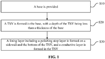
- an embodiment of the application provides a method for manufacturing a semiconductor structure. As shown in FIG. 1 , the method comprises the following operations.
- a base 11 is provided.
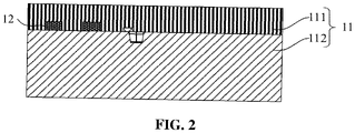
- the base 11 may comprise a substrate 112 and a first dielectric layer 111 on an upper surface of the substrate 112.
- a plurality of device units 12 arranged in an array are formed in the first dielectric layer 111.
- the device units 12 may be memory cells.
- the first dielectric layer 111 may be a silicon nitride layer or a silicon oxide layer.
- a planarization process (for example, a chemical mechanical polishing process), may be performed on an upper surface of the first dielectric layer 111.
- a TSV 13 is formed in the base 11, a depth of the TSV 13 is less than a thickness of the base 11.
- the base 11 comprises an array region and a peripheral region located on a periphery of the array region.
- the TSV 13 in this embodiment is formed in the peripheral region.
- the TSV 13 may be formed in the peripheral region of the base 11 by a photolithography process. As shown in FIG. 3 , the TSV 13 passes through the first dielectric layer 111, and partially extends into the substrate 112.
- a liner layer is formed on a sidewall and the bottom of the TSV 13, and a conductive layer 15 is formed in the TSV 13.
- the liner layer comprises a polish-stop layer.
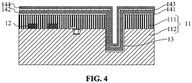
- the liner layer comprises a dielectric filler layer and the polish-stop layer that are sequentially stacked onto one another.
- the operations of forming the liner layer and the conductive layer 15 are as follows.
- a first polish-stop layer 141 is formed on an upper surface of the base 11 as well as the sidewall and bottom of the TSV 13.
- a first dielectric filler layer 142 is formed on a surface of the first polish-stop layer 141.
- a second polish-stop layer 143 is formed on a surface of the first dielectric filler layer 142.
- a second dielectric filler layer 144 is formed on a surface of the second polish-stop layer 143.
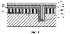
- the conductive layer 15 is formed on a surface of the second dielectric filler layer 144, the conductive layer 15 covers an upper surface of the second dielectric filler layer 144 and entirely fill the TSV 13.
- the conductive layer 15 located above the base 11, the second dielectric filler layer 144 located above the base 11, the second polish-stop layer 143 located above the base 11, and the first dielectric filler layer 142 located above the base 11 are removed.
- the first dielectric filler layer 142 and the second dielectric filler layer 144 may be silicon oxide layers.
- the first polish-stop layer 141 and the second polish-stop layer 143 may be silicon nitride layers or silicon carbon nitride layers.
- the conductive layer 15 may be a copper layer.
- FIG. 4 is a schematic structural sectional view of a semiconductor structure obtained after the liner layer is formed on the sidewall and bottom of the TSV 13.
- FIG. 5 is a schematic sectional view of a semiconductor structure formed after the conductive layer 15 covers the upper surface of the second dielectric filler layer 144 and fills the TSV 13.
- the conductive layer 15 may be formed on the surface of the second dielectric filler layer 144 by an electroplating process.
- the method may further comprise a operation of performing a planarization process, for example, chemical mechanical polishing, on surfaces of the above material layers.
- the polish-stop layer is added in a manufacturing process of the liner layer, so that a polishing progress may be determined by the polish-stop layer and the polishing rate may be adjusted in time in a subsequent polishing process, to prevent excessive polishing and the damage to the conductive layer 15 in the TSV 13.
- the method further comprises the following operations.
- an interconnection through hole 16 is formed, to expose the device units 12.
- FIG. 6 is a schematic sectional view of a semiconductor structure formed after the conductive layer 15 and the second dielectric filler layer 144 located above the base 11 are removed.
- a photoresist layer with a photolithography pattern may be formed on the structure shown in FIG. 6 .
- a position of the photolithography pattern corresponds to the device units 12 in the first dielectric layer 111.
- the second polish-stop layer 143, the first dielectric filler layer 142, the first polish-stop layer 141, and the first dielectric layer 111 are etched in accordance with the photolithography pattern, to form the interconnection through hole 16, as shown in FIG. 7 .
- an interconnection material layer 17 is formed in the interconnection through hole 16 and on an upper surface of the second polish-stop layer 143.
- the interconnection material layer 17 may be at least one of a tungsten layer, an aluminum layer, a copper layer or a titanium nitride layer.
- FIG. 8 is a schematic sectional view of a semiconductor structure obtained after the interconnection material layer 17 is formed.
- the excessive interconnection material layer 17 needs to be removed.
- a polishing device is controlled to polish the portion of the interconnection material layer 17 located on the upper surface of the second polish-stop layer 143, to remove this portion of the interconnection material layer 17.
- a polishing resistance changes.
- the polishing resistance significantly increases.
- the polishing device will be controlled to lower the polishing rate of the polishing device, then the polishing is continued to remove the second polish-stop layer 143 and the first dielectric filler layer 142.
- the polishing resistance changes again.
- FIG. 9 is a schematic sectional view of a semiconductor structure obtained after the interconnection structure 18 is formed.
- the upper surface of the interconnection structure 18 is flush with the upper surface of the first polish-stop layer 141.
- the interconnection structure 18 may be at least one of a tungsten layer, an aluminum layer, a copper layer or a titanium nitride layer.
- the forming the interconnection structure 18 further comprises the following operations.
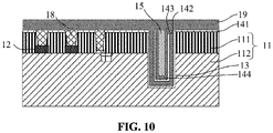
- a second dielectric layer 19 is formed on the upper surface of the first polish-stop layer 141, the upper surface of the interconnection structure 18, an upper surface of the liner layer, and an upper surface of the conductive layer 15.
- FIG. 10 is a schematic sectional view of a semiconductor structure obtained after the second dielectric layer 19 is formed.
- a material of the second dielectric layer 19 may be the same as a material of the first dielectric filler layer 142 or the second dielectric filler layer 144. That is, the second dielectric layer 19 may be a silicon oxide layer.
- trenches 20 are formed in the second dielectric layer 19 to expose the interconnection structure 18 and the conductive layer 15 respectively.
- FIG. 11 is a schematic sectional view of a semiconductor structure obtained after the trenches 20 are formed.
- the trenches 20 may be formed by a photolithography process.
- a metal layer 21 is formed in the trenches 20.
- the metal layer 21 may be a copper layer.
- the metal layer 21 is first formed in the trenches 20 and on an upper surface of the second dielectric layer 19 by an electroplating process. A portion of the metal layer 21 on the upper surface of the second dielectric layer 19 is then removed by a chemical mechanical polishing process. A portion of the metal layer 21 in the trench 20 is retained, and a surface of the metal layer 21 is planarized, to enable the metal layer 21 in the trench 20 to be flush with the upper surface of the second dielectric layer 19.
- the method further comprises the following operations.
- the substrate 112 is thinned from a back side, until the bottom of the conductive layer 15 is exposed.
- the bottom of the conductive layer 15 is exposed, to enable different wafers to be connected by the conductive layer 15 in the TSV 13, so as to implement a vertical interconnect stacking packaging.
- the thinning of the substrate 112 from the back side comprises the following operations.
- the substrate 112 is thinned from a back side by polishing at a first polishing rate, until the polish-stop layer is exposed.
- the substrate 112 is continued to be thinned from the back side by polishing at a second polishing rate, until the bottom of the conductive layer 15 is exposed.
- back side of the substrate 112 is polished at the first polishing rate to reduce the thickness of the substrate.
- a signal indicating that the polishing resistance increases may be detected, and thus the first polish-stop layer 141 is identified.
- the polishing rate is lowered to the second polishing rate, then the polishing continues with the second polishing rate.
- the polishing device comes into contact with the second polish-stop layer 143, a signal indicating that the polishing resistance increases may be detected again, and thus the second polish-stop layer 143 is identified.
- the polishing device may continue to perform polishing at the second polishing rate, until the bottom of the conductive layer 15 is exposed.
- the polishing device may also lower the polishing rate to a third polishing rate, to continue to perform the polishing at the third polishing rate, until the bottom of the conductive layer 15 is exposed.
- the third polishing rate is less than the second polishing rate, and the second polishing rate is less than the first polishing rate.
- the semiconductor structure, obtained after the substrate 112 is thinned from a back side to expose the bottom of the conductive layer 15, is shown in the schematic structural sectional view of FIG. 13 .
- the polish-stop layer is disposed in the liner layer of the TSV 13, so that during the thinning of the substrate 112 from the back side, a polishing progress may be determined by detecting whether the polishing device comes into contact with the polish-stop layer, and the polishing rate may be adjusted in time, to avoid an phenomenon of excessive polishing, thereby preventing the conductive layer 15 from damage and avoiding affecting the electrical performance of the conductive layer 15.
- a width of the interconnection through hole 16 is less than a width of the TSV 13.
- the interconnection through hole 16 is located in the array region, a size of the interconnection through hole 16 usually corresponds to a size of the device unit 12. Because the feature size of the device unit 12 keeps decreasing, the size of the interconnection through hole 16 also correspondingly decreases.
- the TSV 13 is located on a periphery of the array region, and there is no direct relation between the TSV and the size of the device unit 12. The width of the TSV 13 may be appropriately increased, to enable the width of the TSV 13 to be greater than the width of the interconnection through hole 16, so that a resistance of the conductive layer 15 in the TSV 13 can be reduced.
- the semiconductor structure comprises: a base 11, a TSV 13 located in the base 11, a liner layer and a conductive layer 15.
- a depth of the TSV 13 is less than a thickness of the base 11.
- the liner layer is located at least on a sidewall and the bottom of the TSV 13, and the liner layer comprises a polish-stop layer.
- the conductive layer is located in the TSV 13, and entirely fills the TSV 13.
- the base 11 may comprise a substrate 112 and a first dielectric layer 111 on an upper surface of the substrate 112.
- a plurality of device units 12 formed in the first dielectric layer 111 are arranged in an array.
- the device units 12 may be memory cells or may be a front trench isolation structure.
- the first dielectric layer 111 may be a silicon nitride layer or a silicon oxide layer.
- the TSV 13 passes through the first dielectric layer 111, and partially extends into the substrate 112.
- a part of the liner layer is located on the sidewall and bottom of the TSV 13, and another part is located on an upper surface of the first dielectric layer 111.
- the liner layer comprises the polish-stop layer.
- the function of the polish-stop layer lies in that: during the polishing of a back surface (that is, a surface close to the bottom of the TSV 13) of the base 11, a polishing rate may be adjusted in time according to a position of the polish-stop layer, to avoid excessive polishing, so that the precision is increased while the polishing efficiency is improved. For example, before the polishing device comes into contact with the polish-stop layer, the polishing may be performed at a relatively fast polishing rate.
- the polishing device comes into contact with the polish-stop layer, the polishing device receives a signal indicating that a polishing resistance changes. Then, a user may determine a current progress of the polishing, that is, the polishing device already approaches the bottom of the conductive layer 15, and may appropriately decrease a polishing rate, to perform more accurate polishing.
- the liner layer comprises a first polish-stop layer 141, a first dielectric filler layer 142, a second polish-stop layer 143, and a second dielectric filler layer 144 that are sequentially stacked onto one another in a direction from the base 11 to the conductive layer 15.
- the polishing device may more precisely adjust the polishing rate by means of the first polish-stop layer 141 and the second polish-stop layer 143, thereby further improving the polishing efficiency and polishing precision.
- the substrate 112 may be thinned by polishing the back surface at a first polishing rate.
- a signal indicating an increase in the polishing resistance may be detected, and thus the first polish-stop layer 141 is identified.
- the polishing device is controlled to lower the polishing rate to a second polishing rate. Then, the polishing continues with the second polishing rate.
- the polishing device When the polishing device comes into contact with the second polish-stop layer 143, a signal indicating that an increase in the polishing resistance may be detected again, and thus the second polish-stop layer 143 is identified.
- the polishing device may continue to perform polishing at the second polishing rate, until the bottom of the conductive layer 15 is exposed.
- the polishing device may also lower the polishing rate to a third polishing rate, to continue to perform the polishing at the third polishing rate, until the bottom of the conductive layer 15 is exposed.
- the third polishing rate is less than the second polishing rate, and the second polishing rate is less than the first polishing rate.
- a plurality of polish-stop layers are disposed.
- the user may perform polishing at a relatively fast speed with confidence before the polishing device comes into contact with the next polish-stop layer without worrying about the excessive polishing.
- the polishing rate is adjusted only after the polishing device comes into contact with the polish-stop layer, to perform more cautious and precise polishing, so that the polishing efficiency is improved while the polishing precision is ensured.
- the first dielectric filler layer 142 and the second dielectric filler layer 144 both comprise a silicon oxide layer.
- the first polish-stop layer 141 and the second polish-stop layer 143 both comprise a silicon nitride layer or a silicon carbon nitride layer.
- the polish-stop layer is a silicon nitride (Si 3 N 4 ) layer.
- Silicon nitride is a structural ceramic material, has a high hardness and wear resistance, and is very suitable for use as a mask stop layer.
- the polishing device may detect an increase in the polishing resistance, thereby prompting the user to lower the polishing rate, to avoid the excessive polishing.
- the base 11 comprises an array region and a peripheral region located on a periphery of the array region.
- the TSV 13 is located in the peripheral region.
- the base 11 comprises the substrate 112 and the first dielectric layer 111 located on the upper surface of the substrate 112.
- the plurality of device units 12 arranged in an array are formed in the first dielectric layer 111 in the array region.
- the first polish-stop layer 141 extends to the upper surface of the first dielectric layer 111.
- the semiconductor structure further comprises an interconnection structure 18, a second dielectric layer 19 and a metal layer 21. The bottom of the interconnection structure 18 is in contact with the device units 12, an upper surface of the interconnection structure 18 is flush with an upper surface of the first polish-stop layer 141.
- the second dielectric layer 19 is located on the upper surface of the first polish-stop layer 141, an upper surface of the liner layer, and an upper surface of the conductive layer 15.
- the metal layer 21 is located in the second dielectric layer 19, and in contact with the device units 12 and the conductive layer 15.
- the metal layer 21 comprises a plurality of metal structures, which are in contact with the interconnection structure 18 and the conductive layer 15 respectively.
- the metal layer 21 comprises a copper metal structure.
- the interconnection structure 18 comprises at least one of a tungsten layer, an aluminum layer, a copper layer or a titanium nitride layer.
- the device units 12 comprise memory cells.
- the first dielectric layer 111 comprises a silicon nitride layer or a silicon oxide layer.
- the second dielectric layer 19 comprises a silicon oxide layer.
- the semiconductor structure comprises: a base 11, a TSV 13 located in the base 11, a liner layer at least located on a sidewall of the TSV 13 and a conductive layer 15.
- a depth of the TSV 13 is equal to a thickness of the base 11.
- the liner layer comprises a polish-stop layer.
- the conductive layer is located in the TSV 13, and entirely fills the TSV 13.
- the polish-stop layer is formed in the liner layer of the TSV, so that a polishing progress may be determined by the polish-stop layer and a polishing rate may be adjusted in time in a process of polishing a back surface of the base to penetrate the TSV, to prevent damage to the conductive layer in the TSV due to the excessive polishing.
Landscapes
- Internal Circuitry In Semiconductor Integrated Circuit Devices (AREA)
Abstract
Description
- This application claims priority to
Chinese patent application No. 202110500614.6, entitled "SEMICONDUCTOR STRUCTURE AND METHOD FOR MANUFACTURING SEMICONDUCTOR STRUCTURE", filed with the China National Intellectual Property Administration on May 8, 2021 - The application relates to the field of semiconductor devices and manufacturing thereof, and in particular, to a semiconductor structure and a method for manufacturing same.
- With the development of semiconductor technologies, the feature size of an integrated circuit keeps decreasing, and the device interconnection density keeps increasing. Conventional two-dimensional packaging can no longer meet the needs of the industry. Therefore, a Through Silicon Via (TSV)-based vertical interconnect stacking packaging method gradually becomes the development trend of packaging technologies for its key technical advantages of short-range interconnection and high-density integration.
- In an existing TSV technology, during the polishing after a metal material is filled in a TSV, a polishing rate and a polishing thickness cannot be effectively controlled, and an excessive polishing tends to occur.
- According to various embodiments of the application, a semiconductor structure and a method for manufacturing same are provided.
- A method for manufacturing a semiconductor structure comprises: providing a base; forming a TSV in the base, with a depth of the TSV being less than a thickness of the base; and forming a liner layer on a sidewall and the bottom of the TSV, and forming a conductive layer in the TSV, the liner layer comprising a polish-stop layer.
- A semiconductor structure comprises a base, a TSV located in the base, a liner layer at least located on a sidewall and the bottom of the TSV and a conductive layer. A depth of the TSV is less than a thickness of the base. The liner layer comprises a polish-stop layer. The conductive layer is located in the TSV and entirely fills the TSV.
- To describe the technical solutions in the embodiments of the application more clearly, the following briefly introduces the accompanying drawings required for describing the embodiments. Apparently, the accompanying drawings in the following description show merely some embodiments of the application, and a person of ordinary skill in the art may still derive the drawings of other embodiments from these accompanying drawings without creative efforts.
-
FIG. 1 is a flowchart of a method for manufacturing a semiconductor structure according to an embodiment of the application; -
FIG. 2 is a schematic sectional view of a substrate according to an embodiment of the application; -
FIG. 3 is a schematic sectional view of a semiconductor structure obtained after a TSV is formed according to an embodiment of the application; -
FIG. 4 is a schematic sectional view of a semiconductor structure obtained after a liner layer is formed according to an embodiment of the application; -
FIG. 5 is a schematic sectional view of a semiconductor structure obtained after a conductive layer is formed on an upper surface of a second dielectric filler layer and in a TSV according to an embodiment of the application; -
FIG. 6 is a schematic sectional view of a semiconductor structure obtained after a conductive layer is formed in a TSV according to an embodiment of the application; -
FIG. 7 is a schematic structural view of a semiconductor structure obtained after an interconnection through hole is formed according to an embodiment of the application; -
FIG. 8 is a schematic sectional view of a semiconductor structure obtained after an interconnection material layer is formed according to an embodiment of the application; -
FIG. 9 is a schematic sectional view of a semiconductor structure obtained after an interconnection structure is formed according to an embodiment of the application; -
FIG. 10 is a schematic sectional view of a semiconductor structure obtained after a second dielectric layer is formed according to an embodiment of the application; -
FIG. 11 is a schematic sectional view of a semiconductor structure obtained after trenches are formed in a second dielectric layer according to an embodiment of the application; -
FIG. 12 is a schematic sectional view of a semiconductor structure obtained after a metal layer is formed according to an embodiment of the application; and -
FIG. 13 is a schematic sectional view of a semiconductor structure obtained after a substrate is thinned from a back side according to an embodiment of the application. - For ease of understanding of the application, the application is described more completely below with reference to the accompanying drawings. The preferred embodiments of the application are given in the accompanying drawings. However, the application may be implemented in various forms, and is not limited to the embodiments described herein. Rather, these embodiments are provided so that the disclosed content of the application will be understood more thoroughly and completely.
- Unless otherwise defined, the technical terms and scientific terms used herein have the same meanings as how they are generally understood by a person skilled in the art to which the application pertains. The terms used herein in the specification of the application are merely used for describing specific embodiments, but are not intended to limit the application. The term "and/or" used herein encompasses any and all possible combinations of one or more of the associated listed items.
- In describing the location relationship, unless otherwise specified, when an element such as a layer, membrane or substrate is referred to as being "on" another membrane layer, it can be directly on the other membrane layer or there may be an intermediate membrane layer. Further, when a layer is referred to as being "under" another layer, it may be directly below, or there may be one or more intermediate layers. It is also understood that when a layer is referred to as being "between" two layers, it may be the only layer between the two layers, or there may be one or more intermediate layers.
- In the case in which "comprise," "have," and "comprise" described herein are used, another part may also be added unless explicit limitative terms such as "only" and "formed by..." are used. The terms in a singular form may comprise plural forms unless noted to the contrary, and cannot be understood that there is the quantity is 1.
- In an existing TSV technology, during the polishing performed after a metal material is filled in a TSV, a polishing rate and a polishing thickness cannot be effectively controlled, and a problem of the excessive polishing tends to occur. In view of the foregoing problem, an embodiment of the application provides a method for manufacturing a semiconductor structure. As shown in
FIG. 1 , the method comprises the following operations. - At S10, a
base 11 is provided. - In an example, as shown in
FIG. 2 , thebase 11 may comprise asubstrate 112 and a firstdielectric layer 111 on an upper surface of thesubstrate 112. A plurality ofdevice units 12 arranged in an array are formed in the firstdielectric layer 111. Thedevice units 12 may be memory cells. The firstdielectric layer 111 may be a silicon nitride layer or a silicon oxide layer. Optionally, a planarization process (for example, a chemical mechanical polishing process), may be performed on an upper surface of the firstdielectric layer 111. - At S20, a TSV 13 is formed in the
base 11, a depth of the TSV 13 is less than a thickness of thebase 11. - Specifically, the
base 11 comprises an array region and a peripheral region located on a periphery of the array region. The TSV 13 in this embodiment is formed in the peripheral region. In an example, the TSV 13 may be formed in the peripheral region of thebase 11 by a photolithography process. As shown inFIG. 3 , the TSV 13 passes through the firstdielectric layer 111, and partially extends into thesubstrate 112. - At S30, a liner layer is formed on a sidewall and the bottom of the TSV 13, and a
conductive layer 15 is formed in the TSV 13. The liner layer comprises a polish-stop layer. - Specifically, the liner layer comprises a dielectric filler layer and the polish-stop layer that are sequentially stacked onto one another. As shown in
FIG. 4 andFIG. 5 , the operations of forming the liner layer and theconductive layer 15 are as follows. - At S31, a first polish-
stop layer 141 is formed on an upper surface of thebase 11 as well as the sidewall and bottom of the TSV 13. - At S32, a first
dielectric filler layer 142 is formed on a surface of the first polish-stop layer 141. - At S33, a second polish-
stop layer 143 is formed on a surface of the firstdielectric filler layer 142. - At S34, a second
dielectric filler layer 144 is formed on a surface of the second polish-stop layer 143. - At S35, the
conductive layer 15 is formed on a surface of the seconddielectric filler layer 144, theconductive layer 15 covers an upper surface of the seconddielectric filler layer 144 and entirely fill theTSV 13. - At S36, the
conductive layer 15 located above thebase 11, the seconddielectric filler layer 144 located above thebase 11, the second polish-stop layer 143 located above thebase 11, and the firstdielectric filler layer 142 located above thebase 11 are removed. - The first
dielectric filler layer 142 and the seconddielectric filler layer 144 may be silicon oxide layers. The first polish-stop layer 141 and the second polish-stop layer 143 may be silicon nitride layers or silicon carbon nitride layers. Theconductive layer 15 may be a copper layer. - In an example,
FIG. 4 is a schematic structural sectional view of a semiconductor structure obtained after the liner layer is formed on the sidewall and bottom of theTSV 13.FIG. 5 is a schematic sectional view of a semiconductor structure formed after theconductive layer 15 covers the upper surface of the seconddielectric filler layer 144 and fills theTSV 13. Theconductive layer 15 may be formed on the surface of the seconddielectric filler layer 144 by an electroplating process. Optionally, after the first polish-stop layer 141, the firstdielectric filler layer 142, the second polish-stop layer 143, the seconddielectric filler layer 144, and theconductive layer 15 are formed, the method may further comprise a operation of performing a planarization process, for example, chemical mechanical polishing, on surfaces of the above material layers. - In the foregoing method for manufacturing a semiconductor structure, the polish-stop layer is added in a manufacturing process of the liner layer, so that a polishing progress may be determined by the polish-stop layer and the polishing rate may be adjusted in time in a subsequent polishing process, to prevent excessive polishing and the damage to the
conductive layer 15 in theTSV 13. - In an embodiment, after the
conductive layer 15 and the seconddielectric filler layer 144 located above thebase 11 are removed and before the second polish-stop layer 143 located above thebase 11 is removed, the method further comprises the following operations. - At S361, an interconnection through
hole 16 is formed, to expose thedevice units 12. -
FIG. 6 is a schematic sectional view of a semiconductor structure formed after theconductive layer 15 and the seconddielectric filler layer 144 located above thebase 11 are removed. To form the interconnection throughhole 16, a photoresist layer with a photolithography pattern may be formed on the structure shown inFIG. 6 . A position of the photolithography pattern corresponds to thedevice units 12 in thefirst dielectric layer 111. Then the second polish-stop layer 143, the firstdielectric filler layer 142, the first polish-stop layer 141, and thefirst dielectric layer 111 are etched in accordance with the photolithography pattern, to form the interconnection throughhole 16, as shown inFIG. 7 . - At S362, an
interconnection material layer 17 is formed in the interconnection throughhole 16 and on an upper surface of the second polish-stop layer 143. - In an example, the
interconnection material layer 17 may be at least one of a tungsten layer, an aluminum layer, a copper layer or a titanium nitride layer.FIG. 8 is a schematic sectional view of a semiconductor structure obtained after theinterconnection material layer 17 is formed. - At S363, a portion of the
interconnection material layer 17 located on the upper surface of the second polish-stop layer 143 is removed. - At S364, while the second polish-
stop layer 143 located above thebase 11 and the firstdielectric filler layer 142 located above thebase 11 are removed, a portion of theinterconnection material layer 17 located above the first polish-stop layer 141 is removed. A portion of theinterconnection material layer 17 retained in the interconnection throughhole 16 forms aninterconnection structure 18, an upper surface of theinterconnection structure 18 is flush with an upper surface of the first polish-stop layer 141. - To form the
interconnection structure 18, the excessiveinterconnection material layer 17 needs to be removed. Specifically, at first, a polishing device is controlled to polish the portion of theinterconnection material layer 17 located on the upper surface of the second polish-stop layer 143, to remove this portion of theinterconnection material layer 17. When the polishing device comes into contact with the second polish-stop layer 143, a polishing resistance changes. For example, the polishing resistance significantly increases. In this case, the polishing device will be controlled to lower the polishing rate of the polishing device, then the polishing is continued to remove the second polish-stop layer 143 and the firstdielectric filler layer 142. Finally, when the polishing device comes into contact with the first polish-stop layer 141, the polishing resistance changes again. In this case, the polishing device is controlled to stop polishing, to obtain theinterconnection structure 18.FIG. 9 is a schematic sectional view of a semiconductor structure obtained after theinterconnection structure 18 is formed. The upper surface of theinterconnection structure 18 is flush with the upper surface of the first polish-stop layer 141. Theinterconnection structure 18 may be at least one of a tungsten layer, an aluminum layer, a copper layer or a titanium nitride layer. - In an embodiment, the forming the
interconnection structure 18 further comprises the following operations. - At S365, a
second dielectric layer 19 is formed on the upper surface of the first polish-stop layer 141, the upper surface of theinterconnection structure 18, an upper surface of the liner layer, and an upper surface of theconductive layer 15. - In an example,
FIG. 10 is a schematic sectional view of a semiconductor structure obtained after thesecond dielectric layer 19 is formed. A material of thesecond dielectric layer 19 may be the same as a material of the firstdielectric filler layer 142 or the seconddielectric filler layer 144. That is, thesecond dielectric layer 19 may be a silicon oxide layer. - At S366,
trenches 20 are formed in thesecond dielectric layer 19 to expose theinterconnection structure 18 and theconductive layer 15 respectively. - In an example,
FIG. 11 is a schematic sectional view of a semiconductor structure obtained after thetrenches 20 are formed. Thetrenches 20 may be formed by a photolithography process. - At S367, a
metal layer 21 is formed in thetrenches 20. - Optionally, the
metal layer 21 may be a copper layer. Themetal layer 21 is first formed in thetrenches 20 and on an upper surface of thesecond dielectric layer 19 by an electroplating process. A portion of themetal layer 21 on the upper surface of thesecond dielectric layer 19 is then removed by a chemical mechanical polishing process. A portion of themetal layer 21 in thetrench 20 is retained, and a surface of themetal layer 21 is planarized, to enable themetal layer 21 in thetrench 20 to be flush with the upper surface of thesecond dielectric layer 19. - In an embodiment, after the
conductive layer 15 is formed in theTSV 13, the method further comprises the following operations. - At S40, the
substrate 112 is thinned from a back side, until the bottom of theconductive layer 15 is exposed. - The bottom of the
conductive layer 15 is exposed, to enable different wafers to be connected by theconductive layer 15 in theTSV 13, so as to implement a vertical interconnect stacking packaging. Specifically, the thinning of thesubstrate 112 from the back side comprises the following operations. - At S41, the
substrate 112 is thinned from a back side by polishing at a first polishing rate, until the polish-stop layer is exposed. - At S42, the
substrate 112 is continued to be thinned from the back side by polishing at a second polishing rate, until the bottom of theconductive layer 15 is exposed. - S43: the second polishing rate is less than the first polishing rate.
- For example, at first, back side of the
substrate 112 is polished at the first polishing rate to reduce the thickness of the substrate. When the polishing device comes into contact with the first polish-stop layer 141, a signal indicating that the polishing resistance increases may be detected, and thus the first polish-stop layer 141 is identified. The polishing rate is lowered to the second polishing rate, then the polishing continues with the second polishing rate. When the polishing device comes into contact with the second polish-stop layer 143, a signal indicating that the polishing resistance increases may be detected again, and thus the second polish-stop layer 143 is identified. Optionally, the polishing device may continue to perform polishing at the second polishing rate, until the bottom of theconductive layer 15 is exposed. Optionally, the polishing device may also lower the polishing rate to a third polishing rate, to continue to perform the polishing at the third polishing rate, until the bottom of theconductive layer 15 is exposed. The third polishing rate is less than the second polishing rate, and the second polishing rate is less than the first polishing rate. The semiconductor structure, obtained after thesubstrate 112 is thinned from a back side to expose the bottom of theconductive layer 15, is shown in the schematic structural sectional view ofFIG. 13 . - In the method for manufacturing a semiconductor structure, the polish-stop layer is disposed in the liner layer of the
TSV 13, so that during the thinning of thesubstrate 112 from the back side, a polishing progress may be determined by detecting whether the polishing device comes into contact with the polish-stop layer, and the polishing rate may be adjusted in time, to avoid an phenomenon of excessive polishing, thereby preventing theconductive layer 15 from damage and avoiding affecting the electrical performance of theconductive layer 15. - In an embodiment, a width of the interconnection through
hole 16 is less than a width of theTSV 13. The interconnection throughhole 16 is located in the array region, a size of the interconnection throughhole 16 usually corresponds to a size of thedevice unit 12. Because the feature size of thedevice unit 12 keeps decreasing, the size of the interconnection throughhole 16 also correspondingly decreases. TheTSV 13 is located on a periphery of the array region, and there is no direct relation between the TSV and the size of thedevice unit 12. The width of theTSV 13 may be appropriately increased, to enable the width of theTSV 13 to be greater than the width of the interconnection throughhole 16, so that a resistance of theconductive layer 15 in theTSV 13 can be reduced. - Another embodiment of the application further discloses a semiconductor structure. As shown in
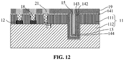
FIG. 12 , the semiconductor structure comprises: a base 11, aTSV 13 located in thebase 11, a liner layer and aconductive layer 15. A depth of theTSV 13 is less than a thickness of thebase 11. The liner layer is located at least on a sidewall and the bottom of theTSV 13, and the liner layer comprises a polish-stop layer. The conductive layer is located in theTSV 13, and entirely fills theTSV 13. - Specifically, as shown in
FIG. 12 , thebase 11 may comprise asubstrate 112 and a firstdielectric layer 111 on an upper surface of thesubstrate 112. A plurality ofdevice units 12 formed in thefirst dielectric layer 111 are arranged in an array. Thedevice units 12 may be memory cells or may be a front trench isolation structure. Thefirst dielectric layer 111 may be a silicon nitride layer or a silicon oxide layer. TheTSV 13 passes through thefirst dielectric layer 111, and partially extends into thesubstrate 112. - In an example, as shown in
FIG. 12 , a part of the liner layer is located on the sidewall and bottom of theTSV 13, and another part is located on an upper surface of thefirst dielectric layer 111. The liner layer comprises the polish-stop layer. The function of the polish-stop layer lies in that: during the polishing of a back surface (that is, a surface close to the bottom of the TSV 13) of thebase 11, a polishing rate may be adjusted in time according to a position of the polish-stop layer, to avoid excessive polishing, so that the precision is increased while the polishing efficiency is improved. For example, before the polishing device comes into contact with the polish-stop layer, the polishing may be performed at a relatively fast polishing rate. There is no risk that theconductive layer 15 will be damaged by the excessive polishing. When the polishing device comes into contact with the polish-stop layer, the polishing device receives a signal indicating that a polishing resistance changes. Then, a user may determine a current progress of the polishing, that is, the polishing device already approaches the bottom of theconductive layer 15, and may appropriately decrease a polishing rate, to perform more accurate polishing. - In an embodiment, the liner layer comprises a first polish-
stop layer 141, a firstdielectric filler layer 142, a second polish-stop layer 143, and a seconddielectric filler layer 144 that are sequentially stacked onto one another in a direction from the base 11 to theconductive layer 15. - Continuing to refer to
FIG. 12 , two polish-stop layers are disposed in the liner layer. The polishing device may more precisely adjust the polishing rate by means of the first polish-stop layer 141 and the second polish-stop layer 143, thereby further improving the polishing efficiency and polishing precision. For example, at first, thesubstrate 112 may be thinned by polishing the back surface at a first polishing rate. When the polishing device comes into contact with the first polish-stop layer 141, a signal indicating an increase in the polishing resistance may be detected, and thus the first polish-stop layer 141 is identified. Then the polishing device is controlled to lower the polishing rate to a second polishing rate. Then, the polishing continues with the second polishing rate. When the polishing device comes into contact with the second polish-stop layer 143, a signal indicating that an increase in the polishing resistance may be detected again, and thus the second polish-stop layer 143 is identified. Optionally, the polishing device may continue to perform polishing at the second polishing rate, until the bottom of theconductive layer 15 is exposed. Optionally, the polishing device may also lower the polishing rate to a third polishing rate, to continue to perform the polishing at the third polishing rate, until the bottom of theconductive layer 15 is exposed. The third polishing rate is less than the second polishing rate, and the second polishing rate is less than the first polishing rate. In the semiconductor structure in this embodiment, a plurality of polish-stop layers are disposed. The user may perform polishing at a relatively fast speed with confidence before the polishing device comes into contact with the next polish-stop layer without worrying about the excessive polishing. The polishing rate is adjusted only after the polishing device comes into contact with the polish-stop layer, to perform more cautious and precise polishing, so that the polishing efficiency is improved while the polishing precision is ensured. - In an embodiment, the first
dielectric filler layer 142 and the seconddielectric filler layer 144 both comprise a silicon oxide layer. The first polish-stop layer 141 and the second polish-stop layer 143 both comprise a silicon nitride layer or a silicon carbon nitride layer. - In an example, the polish-stop layer is a silicon nitride (Si3N4) layer. Silicon nitride is a structural ceramic material, has a high hardness and wear resistance, and is very suitable for use as a mask stop layer. When the polishing device comes into contact with the silicon nitride layer, the polishing device may detect an increase in the polishing resistance, thereby prompting the user to lower the polishing rate, to avoid the excessive polishing.
- In an embodiment, the
base 11 comprises an array region and a peripheral region located on a periphery of the array region. TheTSV 13 is located in the peripheral region. As shown inFIG. 12 , thebase 11 comprises thesubstrate 112 and thefirst dielectric layer 111 located on the upper surface of thesubstrate 112. The plurality ofdevice units 12 arranged in an array are formed in thefirst dielectric layer 111 in the array region. The first polish-stop layer 141 extends to the upper surface of thefirst dielectric layer 111. The semiconductor structure further comprises aninterconnection structure 18, asecond dielectric layer 19 and ametal layer 21. The bottom of theinterconnection structure 18 is in contact with thedevice units 12, an upper surface of theinterconnection structure 18 is flush with an upper surface of the first polish-stop layer 141. Thesecond dielectric layer 19 is located on the upper surface of the first polish-stop layer 141, an upper surface of the liner layer, and an upper surface of theconductive layer 15. Themetal layer 21 is located in thesecond dielectric layer 19, and in contact with thedevice units 12 and theconductive layer 15. - Specifically, as shown in
FIG. 12 , themetal layer 21 comprises a plurality of metal structures, which are in contact with theinterconnection structure 18 and theconductive layer 15 respectively. Themetal layer 21 comprises a copper metal structure. Theinterconnection structure 18 comprises at least one of a tungsten layer, an aluminum layer, a copper layer or a titanium nitride layer. Thedevice units 12 comprise memory cells. Thefirst dielectric layer 111 comprises a silicon nitride layer or a silicon oxide layer. Thesecond dielectric layer 19 comprises a silicon oxide layer. - An embodiment of the application further discloses a semiconductor structure. As shown in
FIG. 13 , the semiconductor structure comprises: a base 11, aTSV 13 located in thebase 11, a liner layer at least located on a sidewall of theTSV 13 and aconductive layer 15. A depth of theTSV 13 is equal to a thickness of thebase 11. The liner layer comprises a polish-stop layer. The conductive layer is located in theTSV 13, and entirely fills theTSV 13. - In the semiconductor structure, the polish-stop layer is formed in the liner layer of the TSV, so that a polishing progress may be determined by the polish-stop layer and a polishing rate may be adjusted in time in a process of polishing a back surface of the base to penetrate the TSV, to prevent damage to the conductive layer in the TSV due to the excessive polishing.
- The technical features in the foregoing embodiments may be randomly combined. For simplicity of description, all possible combinations of the technical features in the foregoing embodiments are not described. However, it should be considered that these combinations of technical features fall within the scope recorded in the specification provided that these combinations of technical features do not have any conflict.
- The foregoing embodiments only describe several embodiments of the application, and their description is specific and detailed, but cannot therefore be understood as a limitation to the claims. It should be noted that for a person of ordinary skill in the art, several variations and improvements may further be made without departing from the concept of the application. These variations and improvements should also be deemed as falling within the scope of protection of the application. Therefore, the scope of protection of the patent of the application shall be subject to the appended claims.
Claims (15)
- A method for manufacturing a semiconductor structure, comprising:providing a base;forming a Through Silicon Via, TSV, in the base, with a depth of the TSV being less than a thickness of the base; andforming a liner layer on a sidewall and a bottom of the TSV, and forming a conductive layer in the TSV, wherein the conductive layer comprises a polish-stop layer.
- The method for manufacturing a semiconductor structure according to claim 1, wherein the forming a liner layer on the sidewall and the bottom of the TSV, and forming the conductive layer in the TSV comprises:forming a first polish-stop layer on an upper surface of the base and the sidewall and the bottom of the TSV;forming a first dielectric filler layer on a surface of the first polish-stop layer;forming a second polish-stop layer on a surface of the first dielectric filler layer;forming a second dielectric filler layer on a surface of the second polish-stop layer;forming the conductive layer on a surface of the second dielectric filler layer, with the conductive layer covering an upper surface of the second dielectric filler layer and entirely filling the TSV; andremoving the conductive layer located above the base, the second dielectric filler layer located above the base, the second polish-stop layer located above the base, and the first dielectric filler layer located above the base.
- The method for manufacturing a semiconductor structure according to claim 2, wherein each of the first dielectric filler layer and the second dielectric filler layer comprises a silicon oxide layer, and each of the first polish-stop layer and the second polish-stop layer comprises a silicon nitride layer or a silicon carbon nitride layer.
- The method for manufacturing a semiconductor structure according to claim 2, wherein the base comprises an array region and a peripheral region located on a periphery of the array region, the TSV is located in the peripheral region; the base comprises a substrate and a first dielectric layer located on an upper surface of the substrate, a plurality of device units arranged in an array are formed in the first dielectric layer in the array region;
after the conductive layer and the second dielectric filler layer located above the base are removed and before the second polish-stop layer located above the base is removed, the method further comprises:forming an interconnection through hole to expose the device units;forming an interconnection material layer in the interconnection through hole and on an upper surface of the second polish-stop layer;removing a portion of the interconnection material layer located on the upper surface of the second polish-stop layer; andremoving the second polish-stop layer located above the base and the first dielectric filler layer located above the base, and removing a portion of the interconnection material layer located above the first polish-stop layer, wherein a portion of the interconnection material layer retained in the interconnection through hole forms an interconnection structure, an upper surface of the interconnection structure is flush with an upper surface of the first polish-stop layer. - The method for manufacturing a semiconductor structure according to claim 4, wherein after the interconnection structure is formed, the method further comprises:forming a second dielectric layer on the upper surface of the first polish-stop layer, the upper surface of the interconnection structure, an upper surface of the liner layer, and an upper surface of the conductive layer;forming trenches in the second dielectric layer to expose the interconnection structure and the conductive layer; andforming a metal layer in the trenches.
- The method for manufacturing a semiconductor structure according to claim 1, wherein after the conductive layer is formed in the TSV, the method further comprises:
thinning the substrate from a back side of the substrate, until the bottom of the conductive layer is exposed. - The method for manufacturing a semiconductor structure according to claim 6, wherein the substrate is thinned from the back side by a polishing process, and the thinning the substrate from a back side of the substrate comprises:thinning the substrate by polishing the back side at a first polishing rate, until the polish-stop layer is exposed; andcontinuing to thin the substrate by polishing the back side at a second polishing rate less than the first polishing rate, until the bottom of the conductive layer is exposed.
- The method for manufacturing a semiconductor structure according to claim 5, wherein the first dielectric layer comprises a silicon nitride layer or a silicon oxide layer, the second dielectric layer comprises a silicon oxide layer, and the interconnection structure comprises at least one of a tungsten layer, an aluminum layer, a copper layer or a titanium nitride layer.
- The method for manufacturing a semiconductor structure according to claim 4, wherein the device units comprise memory cells.
- The method for manufacturing a semiconductor structure according to claim 4, wherein a width of the interconnection through hole is less than a width of the TSV.
- A semiconductor structure, comprising:a base;a Through Silicon Via, TSV, located in the base, a depth of the TSV being less than a thickness of the base;a liner layer at least located on a sidewall and a bottom of the TSV, the liner layer comprising a polish-stop layer; anda conductive layer, located in the TSV and entirely filling the TSV.
- The semiconductor structure according to claim 11, wherein the liner layer comprises a first polish-stop layer, a first dielectric filler layer, a second polish-stop layer and a second dielectric filler layer that are sequentially stacked onto one another in a direction from the base to the conductive layer.
- The semiconductor structure according to claim 12, wherein each of the first dielectric filler layer and the second dielectric filler layer comprises a silicon oxide layer, and each of the first polish-stop layer and the second polish-stop layer comprises a silicon nitride layer or a silicon carbon nitride layer.
- The semiconductor structure according to any one of claims 11 to 13, wherein the base comprises an array region and a peripheral region located on a periphery of the array region, the TSV is located in the peripheral region; the base comprises a substrate and a first dielectric layer located on an upper surface of the substrate, a plurality of device units arranged in an array are formed in the first dielectric layer in the array region; the first polish-stop layer extends to an upper surface of the first dielectric layer;
wherein the semiconductor structure further comprises:an interconnection structure, a bottom of the interconnection structure being in contact with the device units, an upper surface of the interconnection structure being flush with an upper surface of the first polish-stop layer;a second dielectric layer, located on the upper surface of the first polish-stop layer, an upper surface of the liner layer and an upper surface of the conductive layer;a metal layer, located in the second dielectric layer and in contact with the device units and the conductive layer. - The semiconductor structure according to claim 14, wherein the first dielectric layer comprises a silicon nitride layer or a silicon oxide layer, the second dielectric layer comprises a silicon oxide layer, the interconnection structure comprises at least one of a tungsten layer, an aluminum layer, a copper layer or a titanium nitride layer; and the device units comprise memory cells.
Applications Claiming Priority (2)
| Application Number | Priority Date | Filing Date | Title |
|---|---|---|---|
| CN202110500614.6A CN115312449A (en) | 2021-05-08 | 2021-05-08 | Semiconductor structure and preparation method thereof |
| PCT/CN2021/120247 WO2022237044A1 (en) | 2021-05-08 | 2021-09-24 | Semiconductor structure and preparation method therefor |
Publications (3)
| Publication Number | Publication Date |
|---|---|
| EP4117029A1 true EP4117029A1 (en) | 2023-01-11 |
| EP4117029A4 EP4117029A4 (en) | 2023-01-18 |
| EP4117029B1 EP4117029B1 (en) | 2024-01-24 |
Family
ID=83900662
Family Applications (1)
| Application Number | Title | Priority Date | Filing Date |
|---|---|---|---|
| EP21870475.7A Active EP4117029B1 (en) | 2021-05-08 | 2021-09-24 | Semiconductor structure and preparation method therefor |
Country Status (2)
| Country | Link |
|---|---|
| US (1) | US12243779B2 (en) |
| EP (1) | EP4117029B1 (en) |
Family Cites Families (10)
| Publication number | Priority date | Publication date | Assignee | Title |
|---|---|---|---|---|
| US8405222B2 (en) * | 2010-06-28 | 2013-03-26 | Globalfoundries Singapore Pte. Ltd. | Integrated circuit system with via and method of manufacture thereof |
| US8367553B2 (en) * | 2010-12-07 | 2013-02-05 | United Microelectronics Corp. | Method for manufacturing through-silicon via |
| JP2012216812A (en) * | 2011-03-31 | 2012-11-08 | Elpida Memory Inc | Semiconductor device and manufacturing method of the same |
| US8487410B2 (en) * | 2011-04-13 | 2013-07-16 | Taiwan Semiconductor Manufacturing Company, Ltd. | Through-silicon vias for semicondcutor substrate and method of manufacture |
| TW201342526A (en) | 2012-04-13 | 2013-10-16 | 聯華電子股份有限公司 | Piercing conductor structure and its preparation method |
| CN103545275B (en) | 2012-07-12 | 2016-02-17 | 中芯国际集成电路制造(上海)有限公司 | Silicon through hole encapsulating structure and formation method |
| KR101932660B1 (en) | 2012-09-12 | 2018-12-26 | 삼성전자 주식회사 | Integrated circuit device having through silicon via structure and method of manufacturing the same |
| US9287197B2 (en) * | 2013-03-15 | 2016-03-15 | Globalfoundries Singapore Pte. Ltd. | Through silicon vias |
| KR102497205B1 (en) | 2016-03-03 | 2023-02-09 | 삼성전자주식회사 | Semiconductor devices having through electrodes and methods for fabricating the same |
| KR102505853B1 (en) | 2016-07-06 | 2023-03-03 | 삼성전자 주식회사 | Semiconductor package |
-
2021
- 2021-09-24 EP EP21870475.7A patent/EP4117029B1/en active Active
-
2022
- 2022-03-08 US US17/689,000 patent/US12243779B2/en active Active
Also Published As
| Publication number | Publication date |
|---|---|
| US12243779B2 (en) | 2025-03-04 |
| US20220359291A1 (en) | 2022-11-10 |
| EP4117029B1 (en) | 2024-01-24 |
| EP4117029A4 (en) | 2023-01-18 |
Similar Documents
| Publication | Publication Date | Title |
|---|---|---|
| KR100383504B1 (en) | Semiconductor device and method of producing the same | |
| US11342221B2 (en) | Semiconductor device | |
| US11217457B2 (en) | Method of fabricating a semiconductor device | |
| CN1391701A (en) | Self-aligned method of forming deep trenches in shallow trenches to isolate semiconductor devices | |
| CN103681452A (en) | Trench Insulation Process | |
| JP4456027B2 (en) | Method for manufacturing through conductor | |
| US20090176365A1 (en) | Contact formation | |
| JP3645129B2 (en) | Manufacturing method of semiconductor device | |
| KR100518150B1 (en) | Semiconductor workpiece and method of forming alignment mark thereon for enhancing alignment mark contrast | |
| US8629514B2 (en) | Methods and structures for customized STI structures in semiconductor devices | |
| EP4117029B1 (en) | Semiconductor structure and preparation method therefor | |
| CN112185969B (en) | Three-dimensional memory structure and preparation method thereof | |
| US7291562B2 (en) | Method to form topography in a deposited layer above a substrate | |
| WO2022237044A1 (en) | Semiconductor structure and preparation method therefor | |
| US6444581B1 (en) | AB etch endpoint by ABFILL compensation | |
| CN108520863B (en) | Method for manufacturing shallow trench insulation structure | |
| US7282421B2 (en) | Methods for reducing a thickness variation of a nitride layer formed in a shallow trench isolation CMP process and for forming a device isolation film of a semiconductor device | |
| KR100583508B1 (en) | Teos assisted oxide cmp process | |
| KR101102052B1 (en) | Semiconductor element and formation method thereof | |
| CN112768457B (en) | Method and mask for forming three-dimensional memory structure | |
| CN115312448B (en) | Semiconductor structure and method for manufacturing the same | |
| KR100875350B1 (en) | STI Formation Method to Prevent Divot | |
| KR101016352B1 (en) | Device Separator Formation Method of Semiconductor Device | |
| CN120164841A (en) | Semiconductor element forming method and semiconductor element | |
| KR20030001086A (en) | Method for forming landing plug contact in semiconductor device |
Legal Events
| Date | Code | Title | Description |
|---|---|---|---|
| STAA | Information on the status of an ep patent application or granted ep patent |
Free format text: STATUS: UNKNOWN |
|
| STAA | Information on the status of an ep patent application or granted ep patent |
Free format text: STATUS: THE INTERNATIONAL PUBLICATION HAS BEEN MADE |
|
| PUAI | Public reference made under article 153(3) epc to a published international application that has entered the european phase |
Free format text: ORIGINAL CODE: 0009012 |
|
| STAA | Information on the status of an ep patent application or granted ep patent |
Free format text: STATUS: REQUEST FOR EXAMINATION WAS MADE |
|
| 17P | Request for examination filed |
Effective date: 20220328 |
|
| AK | Designated contracting states |
Kind code of ref document: A1 Designated state(s): AL AT BE BG CH CY CZ DE DK EE ES FI FR GB GR HR HU IE IS IT LI LT LU LV MC MK MT NL NO PL PT RO RS SE SI SK SM TR |
|
| A4 | Supplementary search report drawn up and despatched |
Effective date: 20221219 |
|
| RIC1 | Information provided on ipc code assigned before grant |
Ipc: H01L 23/48 20060101ALI20221213BHEP Ipc: H01L 21/768 20060101AFI20221213BHEP |
|
| RIC1 | Information provided on ipc code assigned before grant |
Ipc: H01L 21/321 20060101ALN20230628BHEP Ipc: H01L 23/48 20060101ALI20230628BHEP Ipc: H01L 21/768 20060101AFI20230628BHEP |
|
| RIC1 | Information provided on ipc code assigned before grant |
Ipc: H01L 21/321 20060101ALN20230721BHEP Ipc: H01L 23/48 20060101ALI20230721BHEP Ipc: H01L 21/768 20060101AFI20230721BHEP |
|
| GRAP | Despatch of communication of intention to grant a patent |
Free format text: ORIGINAL CODE: EPIDOSNIGR1 |
|
| STAA | Information on the status of an ep patent application or granted ep patent |
Free format text: STATUS: GRANT OF PATENT IS INTENDED |
|
| DAV | Request for validation of the european patent (deleted) | ||
| DAX | Request for extension of the european patent (deleted) | ||
| INTG | Intention to grant announced |
Effective date: 20230905 |
|
| P01 | Opt-out of the competence of the unified patent court (upc) registered |
Effective date: 20231018 |
|
| GRAS | Grant fee paid |
Free format text: ORIGINAL CODE: EPIDOSNIGR3 |
|
| GRAA | (expected) grant |
Free format text: ORIGINAL CODE: 0009210 |
|
| STAA | Information on the status of an ep patent application or granted ep patent |
Free format text: STATUS: THE PATENT HAS BEEN GRANTED |
|
| AK | Designated contracting states |
Kind code of ref document: B1 Designated state(s): AL AT BE BG CH CY CZ DE DK EE ES FI FR GB GR HR HU IE IS IT LI LT LU LV MC MK MT NL NO PL PT RO RS SE SI SK SM TR |
|
| REG | Reference to a national code |
Ref country code: GB Ref legal event code: FG4D |
|
| REG | Reference to a national code |
Ref country code: CH Ref legal event code: EP |
|
| REG | Reference to a national code |
Ref country code: DE Ref legal event code: R096 Ref document number: 602021008799 Country of ref document: DE |
|
| REG | Reference to a national code |
Ref country code: IE Ref legal event code: FG4D |
|
| REG | Reference to a national code |
Ref country code: LT Ref legal event code: MG9D |
|
| REG | Reference to a national code |
Ref country code: NL Ref legal event code: MP Effective date: 20240124 |
|
| PG25 | Lapsed in a contracting state [announced via postgrant information from national office to epo] |
Ref country code: NL Free format text: LAPSE BECAUSE OF FAILURE TO SUBMIT A TRANSLATION OF THE DESCRIPTION OR TO PAY THE FEE WITHIN THE PRESCRIBED TIME-LIMIT Effective date: 20240124 |
|
| PG25 | Lapsed in a contracting state [announced via postgrant information from national office to epo] |
Ref country code: NL Free format text: LAPSE BECAUSE OF FAILURE TO SUBMIT A TRANSLATION OF THE DESCRIPTION OR TO PAY THE FEE WITHIN THE PRESCRIBED TIME-LIMIT Effective date: 20240124 |
|
| PG25 | Lapsed in a contracting state [announced via postgrant information from national office to epo] |
Ref country code: IS Free format text: LAPSE BECAUSE OF FAILURE TO SUBMIT A TRANSLATION OF THE DESCRIPTION OR TO PAY THE FEE WITHIN THE PRESCRIBED TIME-LIMIT Effective date: 20240524 |
|
| PG25 | Lapsed in a contracting state [announced via postgrant information from national office to epo] |
Ref country code: LT Free format text: LAPSE BECAUSE OF FAILURE TO SUBMIT A TRANSLATION OF THE DESCRIPTION OR TO PAY THE FEE WITHIN THE PRESCRIBED TIME-LIMIT Effective date: 20240124 |
|
| PG25 | Lapsed in a contracting state [announced via postgrant information from national office to epo] |
Ref country code: GR Free format text: LAPSE BECAUSE OF FAILURE TO SUBMIT A TRANSLATION OF THE DESCRIPTION OR TO PAY THE FEE WITHIN THE PRESCRIBED TIME-LIMIT Effective date: 20240425 |
|
| REG | Reference to a national code |
Ref country code: AT Ref legal event code: MK05 Ref document number: 1652871 Country of ref document: AT Kind code of ref document: T Effective date: 20240124 |
|
| PG25 | Lapsed in a contracting state [announced via postgrant information from national office to epo] |
Ref country code: HR Free format text: LAPSE BECAUSE OF FAILURE TO SUBMIT A TRANSLATION OF THE DESCRIPTION OR TO PAY THE FEE WITHIN THE PRESCRIBED TIME-LIMIT Effective date: 20240124 Ref country code: RS Free format text: LAPSE BECAUSE OF FAILURE TO SUBMIT A TRANSLATION OF THE DESCRIPTION OR TO PAY THE FEE WITHIN THE PRESCRIBED TIME-LIMIT Effective date: 20240424 |
|
| PG25 | Lapsed in a contracting state [announced via postgrant information from national office to epo] |
Ref country code: ES Free format text: LAPSE BECAUSE OF FAILURE TO SUBMIT A TRANSLATION OF THE DESCRIPTION OR TO PAY THE FEE WITHIN THE PRESCRIBED TIME-LIMIT Effective date: 20240124 |
|
| PG25 | Lapsed in a contracting state [announced via postgrant information from national office to epo] |
Ref country code: AT Free format text: LAPSE BECAUSE OF FAILURE TO SUBMIT A TRANSLATION OF THE DESCRIPTION OR TO PAY THE FEE WITHIN THE PRESCRIBED TIME-LIMIT Effective date: 20240124 |
|
| PG25 | Lapsed in a contracting state [announced via postgrant information from national office to epo] |
Ref country code: RS Free format text: LAPSE BECAUSE OF FAILURE TO SUBMIT A TRANSLATION OF THE DESCRIPTION OR TO PAY THE FEE WITHIN THE PRESCRIBED TIME-LIMIT Effective date: 20240424 Ref country code: NO Free format text: LAPSE BECAUSE OF FAILURE TO SUBMIT A TRANSLATION OF THE DESCRIPTION OR TO PAY THE FEE WITHIN THE PRESCRIBED TIME-LIMIT Effective date: 20240424 Ref country code: LT Free format text: LAPSE BECAUSE OF FAILURE TO SUBMIT A TRANSLATION OF THE DESCRIPTION OR TO PAY THE FEE WITHIN THE PRESCRIBED TIME-LIMIT Effective date: 20240124 Ref country code: IS Free format text: LAPSE BECAUSE OF FAILURE TO SUBMIT A TRANSLATION OF THE DESCRIPTION OR TO PAY THE FEE WITHIN THE PRESCRIBED TIME-LIMIT Effective date: 20240524 Ref country code: HR Free format text: LAPSE BECAUSE OF FAILURE TO SUBMIT A TRANSLATION OF THE DESCRIPTION OR TO PAY THE FEE WITHIN THE PRESCRIBED TIME-LIMIT Effective date: 20240124 Ref country code: GR Free format text: LAPSE BECAUSE OF FAILURE TO SUBMIT A TRANSLATION OF THE DESCRIPTION OR TO PAY THE FEE WITHIN THE PRESCRIBED TIME-LIMIT Effective date: 20240425 Ref country code: FI Free format text: LAPSE BECAUSE OF FAILURE TO SUBMIT A TRANSLATION OF THE DESCRIPTION OR TO PAY THE FEE WITHIN THE PRESCRIBED TIME-LIMIT Effective date: 20240124 Ref country code: ES Free format text: LAPSE BECAUSE OF FAILURE TO SUBMIT A TRANSLATION OF THE DESCRIPTION OR TO PAY THE FEE WITHIN THE PRESCRIBED TIME-LIMIT Effective date: 20240124 Ref country code: BG Free format text: LAPSE BECAUSE OF FAILURE TO SUBMIT A TRANSLATION OF THE DESCRIPTION OR TO PAY THE FEE WITHIN THE PRESCRIBED TIME-LIMIT Effective date: 20240124 Ref country code: AT Free format text: LAPSE BECAUSE OF FAILURE TO SUBMIT A TRANSLATION OF THE DESCRIPTION OR TO PAY THE FEE WITHIN THE PRESCRIBED TIME-LIMIT Effective date: 20240124 |
|
| PG25 | Lapsed in a contracting state [announced via postgrant information from national office to epo] |
Ref country code: PT Free format text: LAPSE BECAUSE OF FAILURE TO SUBMIT A TRANSLATION OF THE DESCRIPTION OR TO PAY THE FEE WITHIN THE PRESCRIBED TIME-LIMIT Effective date: 20240524 Ref country code: PL Free format text: LAPSE BECAUSE OF FAILURE TO SUBMIT A TRANSLATION OF THE DESCRIPTION OR TO PAY THE FEE WITHIN THE PRESCRIBED TIME-LIMIT Effective date: 20240124 |
|
| PG25 | Lapsed in a contracting state [announced via postgrant information from national office to epo] |
Ref country code: SE Free format text: LAPSE BECAUSE OF FAILURE TO SUBMIT A TRANSLATION OF THE DESCRIPTION OR TO PAY THE FEE WITHIN THE PRESCRIBED TIME-LIMIT Effective date: 20240124 Ref country code: PT Free format text: LAPSE BECAUSE OF FAILURE TO SUBMIT A TRANSLATION OF THE DESCRIPTION OR TO PAY THE FEE WITHIN THE PRESCRIBED TIME-LIMIT Effective date: 20240524 Ref country code: PL Free format text: LAPSE BECAUSE OF FAILURE TO SUBMIT A TRANSLATION OF THE DESCRIPTION OR TO PAY THE FEE WITHIN THE PRESCRIBED TIME-LIMIT Effective date: 20240124 Ref country code: LV Free format text: LAPSE BECAUSE OF FAILURE TO SUBMIT A TRANSLATION OF THE DESCRIPTION OR TO PAY THE FEE WITHIN THE PRESCRIBED TIME-LIMIT Effective date: 20240124 |
|
| PG25 | Lapsed in a contracting state [announced via postgrant information from national office to epo] |
Ref country code: DK Free format text: LAPSE BECAUSE OF FAILURE TO SUBMIT A TRANSLATION OF THE DESCRIPTION OR TO PAY THE FEE WITHIN THE PRESCRIBED TIME-LIMIT Effective date: 20240124 |
|
| PG25 | Lapsed in a contracting state [announced via postgrant information from national office to epo] |
Ref country code: SM Free format text: LAPSE BECAUSE OF FAILURE TO SUBMIT A TRANSLATION OF THE DESCRIPTION OR TO PAY THE FEE WITHIN THE PRESCRIBED TIME-LIMIT Effective date: 20240124 |
|
| PG25 | Lapsed in a contracting state [announced via postgrant information from national office to epo] |
Ref country code: EE Free format text: LAPSE BECAUSE OF FAILURE TO SUBMIT A TRANSLATION OF THE DESCRIPTION OR TO PAY THE FEE WITHIN THE PRESCRIBED TIME-LIMIT Effective date: 20240124 Ref country code: CZ Free format text: LAPSE BECAUSE OF FAILURE TO SUBMIT A TRANSLATION OF THE DESCRIPTION OR TO PAY THE FEE WITHIN THE PRESCRIBED TIME-LIMIT Effective date: 20240124 |
|
| REG | Reference to a national code |
Ref country code: DE Ref legal event code: R097 Ref document number: 602021008799 Country of ref document: DE |
|
| PG25 | Lapsed in a contracting state [announced via postgrant information from national office to epo] |
Ref country code: SK Free format text: LAPSE BECAUSE OF FAILURE TO SUBMIT A TRANSLATION OF THE DESCRIPTION OR TO PAY THE FEE WITHIN THE PRESCRIBED TIME-LIMIT Effective date: 20240124 |
|
| PG25 | Lapsed in a contracting state [announced via postgrant information from national office to epo] |
Ref country code: SM Free format text: LAPSE BECAUSE OF FAILURE TO SUBMIT A TRANSLATION OF THE DESCRIPTION OR TO PAY THE FEE WITHIN THE PRESCRIBED TIME-LIMIT Effective date: 20240124 Ref country code: SK Free format text: LAPSE BECAUSE OF FAILURE TO SUBMIT A TRANSLATION OF THE DESCRIPTION OR TO PAY THE FEE WITHIN THE PRESCRIBED TIME-LIMIT Effective date: 20240124 Ref country code: EE Free format text: LAPSE BECAUSE OF FAILURE TO SUBMIT A TRANSLATION OF THE DESCRIPTION OR TO PAY THE FEE WITHIN THE PRESCRIBED TIME-LIMIT Effective date: 20240124 Ref country code: DK Free format text: LAPSE BECAUSE OF FAILURE TO SUBMIT A TRANSLATION OF THE DESCRIPTION OR TO PAY THE FEE WITHIN THE PRESCRIBED TIME-LIMIT Effective date: 20240124 Ref country code: CZ Free format text: LAPSE BECAUSE OF FAILURE TO SUBMIT A TRANSLATION OF THE DESCRIPTION OR TO PAY THE FEE WITHIN THE PRESCRIBED TIME-LIMIT Effective date: 20240124 |
|
| PLBE | No opposition filed within time limit |
Free format text: ORIGINAL CODE: 0009261 |
|
| STAA | Information on the status of an ep patent application or granted ep patent |
Free format text: STATUS: NO OPPOSITION FILED WITHIN TIME LIMIT |
|
| PG25 | Lapsed in a contracting state [announced via postgrant information from national office to epo] |
Ref country code: IT Free format text: LAPSE BECAUSE OF FAILURE TO SUBMIT A TRANSLATION OF THE DESCRIPTION OR TO PAY THE FEE WITHIN THE PRESCRIBED TIME-LIMIT Effective date: 20240124 |
|
| PG25 | Lapsed in a contracting state [announced via postgrant information from national office to epo] |
Ref country code: IT Free format text: LAPSE BECAUSE OF FAILURE TO SUBMIT A TRANSLATION OF THE DESCRIPTION OR TO PAY THE FEE WITHIN THE PRESCRIBED TIME-LIMIT Effective date: 20240124 |
|
| 26N | No opposition filed |
Effective date: 20241025 |
|
| PG25 | Lapsed in a contracting state [announced via postgrant information from national office to epo] |
Ref country code: SI Free format text: LAPSE BECAUSE OF FAILURE TO SUBMIT A TRANSLATION OF THE DESCRIPTION OR TO PAY THE FEE WITHIN THE PRESCRIBED TIME-LIMIT Effective date: 20240124 Ref country code: MC Free format text: LAPSE BECAUSE OF FAILURE TO SUBMIT A TRANSLATION OF THE DESCRIPTION OR TO PAY THE FEE WITHIN THE PRESCRIBED TIME-LIMIT Effective date: 20240124 |
|
| REG | Reference to a national code |
Ref country code: CH Ref legal event code: PL |
|
| PG25 | Lapsed in a contracting state [announced via postgrant information from national office to epo] |
Ref country code: LU Free format text: LAPSE BECAUSE OF NON-PAYMENT OF DUE FEES Effective date: 20240924 |
|
| REG | Reference to a national code |
Ref country code: BE Ref legal event code: MM Effective date: 20240930 |
|
| PG25 | Lapsed in a contracting state [announced via postgrant information from national office to epo] |
Ref country code: BE Free format text: LAPSE BECAUSE OF NON-PAYMENT OF DUE FEES Effective date: 20240930 |
|
| PG25 | Lapsed in a contracting state [announced via postgrant information from national office to epo] |
Ref country code: FR Free format text: LAPSE BECAUSE OF NON-PAYMENT OF DUE FEES Effective date: 20240930 |
|
| PG25 | Lapsed in a contracting state [announced via postgrant information from national office to epo] |
Ref country code: CH Free format text: LAPSE BECAUSE OF NON-PAYMENT OF DUE FEES Effective date: 20240930 |
|
| PG25 | Lapsed in a contracting state [announced via postgrant information from national office to epo] |
Ref country code: IE Free format text: LAPSE BECAUSE OF NON-PAYMENT OF DUE FEES Effective date: 20240924 |
|
| PGFP | Annual fee paid to national office [announced via postgrant information from national office to epo] |
Ref country code: DE Payment date: 20250919 Year of fee payment: 5 |
|
| PG25 | Lapsed in a contracting state [announced via postgrant information from national office to epo] |
Ref country code: RO Free format text: LAPSE BECAUSE OF FAILURE TO SUBMIT A TRANSLATION OF THE DESCRIPTION OR TO PAY THE FEE WITHIN THE PRESCRIBED TIME-LIMIT Effective date: 20240124 |
|
| REG | Reference to a national code |
Ref country code: DE Ref legal event code: R079 Ref document number: 602021008799 Country of ref document: DE Free format text: PREVIOUS MAIN CLASS: H01L0021768000 Ipc: H10W0020000000 |
|
| PG25 | Lapsed in a contracting state [announced via postgrant information from national office to epo] |
Ref country code: CY Free format text: LAPSE BECAUSE OF FAILURE TO SUBMIT A TRANSLATION OF THE DESCRIPTION OR TO PAY THE FEE WITHIN THE PRESCRIBED TIME-LIMIT; INVALID AB INITIO Effective date: 20210924 |
|
| PG25 | Lapsed in a contracting state [announced via postgrant information from national office to epo] |
Ref country code: HU Free format text: LAPSE BECAUSE OF FAILURE TO SUBMIT A TRANSLATION OF THE DESCRIPTION OR TO PAY THE FEE WITHIN THE PRESCRIBED TIME-LIMIT; INVALID AB INITIO Effective date: 20210924 |