EP4116877B1 - Display assembly, display device, and fingerprint recognition method - Google Patents
Display assembly, display device, and fingerprint recognition method Download PDFInfo
- Publication number
- EP4116877B1 EP4116877B1 EP21780145.5A EP21780145A EP4116877B1 EP 4116877 B1 EP4116877 B1 EP 4116877B1 EP 21780145 A EP21780145 A EP 21780145A EP 4116877 B1 EP4116877 B1 EP 4116877B1
- Authority
- EP
- European Patent Office
- Prior art keywords
- fingerprint recognition
- fingerprint
- signal line
- gate
- active layer
- Prior art date
- Legal status (The legal status is an assumption and is not a legal conclusion. Google has not performed a legal analysis and makes no representation as to the accuracy of the status listed.)
- Active
Links
Images




Classifications
-
- H—ELECTRICITY
- H10—SEMICONDUCTOR DEVICES; ELECTRIC SOLID-STATE DEVICES NOT OTHERWISE PROVIDED FOR
- H10K—ORGANIC ELECTRIC SOLID-STATE DEVICES
- H10K59/00—Integrated devices, or assemblies of multiple devices, comprising at least one organic light-emitting element covered by group H10K50/00
- H10K59/40—OLEDs integrated with touch screens
-
- G—PHYSICS
- G02—OPTICS
- G02F—OPTICAL DEVICES OR ARRANGEMENTS FOR THE CONTROL OF LIGHT BY MODIFICATION OF THE OPTICAL PROPERTIES OF THE MEDIA OF THE ELEMENTS INVOLVED THEREIN; NON-LINEAR OPTICS; FREQUENCY-CHANGING OF LIGHT; OPTICAL LOGIC ELEMENTS; OPTICAL ANALOGUE/DIGITAL CONVERTERS
- G02F1/00—Devices or arrangements for the control of the intensity, colour, phase, polarisation or direction of light arriving from an independent light source, e.g. switching, gating or modulating; Non-linear optics
- G02F1/01—Devices or arrangements for the control of the intensity, colour, phase, polarisation or direction of light arriving from an independent light source, e.g. switching, gating or modulating; Non-linear optics for the control of the intensity, phase, polarisation or colour
- G02F1/13—Devices or arrangements for the control of the intensity, colour, phase, polarisation or direction of light arriving from an independent light source, e.g. switching, gating or modulating; Non-linear optics for the control of the intensity, phase, polarisation or colour based on liquid crystals, e.g. single liquid crystal display cells
- G02F1/133—Constructional arrangements; Operation of liquid crystal cells; Circuit arrangements
- G02F1/1333—Constructional arrangements; Manufacturing methods
- G02F1/13338—Input devices, e.g. touch panels
-
- G—PHYSICS
- G06—COMPUTING OR CALCULATING; COUNTING
- G06V—IMAGE OR VIDEO RECOGNITION OR UNDERSTANDING
- G06V40/00—Recognition of biometric, human-related or animal-related patterns in image or video data
- G06V40/10—Human or animal bodies, e.g. vehicle occupants or pedestrians; Body parts, e.g. hands
- G06V40/12—Fingerprints or palmprints
- G06V40/13—Sensors therefor
- G06V40/1318—Sensors therefor using electro-optical elements or layers, e.g. electroluminescent sensing
-
- H—ELECTRICITY
- H10—SEMICONDUCTOR DEVICES; ELECTRIC SOLID-STATE DEVICES NOT OTHERWISE PROVIDED FOR
- H10K—ORGANIC ELECTRIC SOLID-STATE DEVICES
- H10K39/00—Integrated devices, or assemblies of multiple devices, comprising at least one organic radiation-sensitive element covered by group H10K30/00
- H10K39/30—Devices controlled by radiation
- H10K39/32—Organic image sensors
- H10K39/34—Organic image sensors integrated with organic light-emitting diodes [OLED]
-
- H—ELECTRICITY
- H10—SEMICONDUCTOR DEVICES; ELECTRIC SOLID-STATE DEVICES NOT OTHERWISE PROVIDED FOR
- H10K—ORGANIC ELECTRIC SOLID-STATE DEVICES
- H10K59/00—Integrated devices, or assemblies of multiple devices, comprising at least one organic light-emitting element covered by group H10K50/00
- H10K59/10—OLED displays
- H10K59/12—Active-matrix OLED [AMOLED] displays
- H10K59/123—Connection of the pixel electrodes to the thin film transistors [TFT]
-
- H—ELECTRICITY
- H10—SEMICONDUCTOR DEVICES; ELECTRIC SOLID-STATE DEVICES NOT OTHERWISE PROVIDED FOR
- H10K—ORGANIC ELECTRIC SOLID-STATE DEVICES
- H10K59/00—Integrated devices, or assemblies of multiple devices, comprising at least one organic light-emitting element covered by group H10K50/00
- H10K59/10—OLED displays
- H10K59/12—Active-matrix OLED [AMOLED] displays
- H10K59/131—Interconnections, e.g. wiring lines or terminals
-
- H—ELECTRICITY
- H10—SEMICONDUCTOR DEVICES; ELECTRIC SOLID-STATE DEVICES NOT OTHERWISE PROVIDED FOR
- H10K—ORGANIC ELECTRIC SOLID-STATE DEVICES
- H10K59/00—Integrated devices, or assemblies of multiple devices, comprising at least one organic light-emitting element covered by group H10K50/00
- H10K59/60—OLEDs integrated with inorganic light-sensitive elements, e.g. with inorganic solar cells or inorganic photodiodes
-
- H—ELECTRICITY
- H10—SEMICONDUCTOR DEVICES; ELECTRIC SOLID-STATE DEVICES NOT OTHERWISE PROVIDED FOR
- H10K—ORGANIC ELECTRIC SOLID-STATE DEVICES
- H10K59/00—Integrated devices, or assemblies of multiple devices, comprising at least one organic light-emitting element covered by group H10K50/00
- H10K59/60—OLEDs integrated with inorganic light-sensitive elements, e.g. with inorganic solar cells or inorganic photodiodes
- H10K59/65—OLEDs integrated with inorganic image sensors
-
- H—ELECTRICITY
- H10—SEMICONDUCTOR DEVICES; ELECTRIC SOLID-STATE DEVICES NOT OTHERWISE PROVIDED FOR
- H10K—ORGANIC ELECTRIC SOLID-STATE DEVICES
- H10K59/00—Integrated devices, or assemblies of multiple devices, comprising at least one organic light-emitting element covered by group H10K50/00
- H10K59/10—OLED displays
- H10K59/12—Active-matrix OLED [AMOLED] displays
Definitions
- This application relates to the field of display technologies, and more specifically, to a display assembly, a display apparatus, and a fingerprint recognition method.
- An optical fingerprint recognition module is disposed on a back side of a substrate of a display panel, and light emitted by a fingerprint recognition light source irradiates to a finger. After being reflected by the finger, the light penetrates through the display panel, and then is received by a photosensitive element, to convert an optical signal into an electrical signal. This implements fingerprint recognition.
- a solution in the conventional technology after light used for fingerprint recognition penetrates through an entire display panel in a thickness direction of the display panel, light loss is large. This seriously affects an amount of light received by the photosensitive element, and further affects accuracy of fingerprint recognition.
- CN 110 286 796 A discloses a display assembly comprising a display panel and a fingerprint recognition module.
- this application provides a display assembly, a display apparatus, and a fingerprint recognition method, to resolve a technical problem of low fingerprint recognition accuracy in the conventional technology.
- an embodiment of this application provides a display assembly, including a display panel and a fingerprint recognition module located on a light-emitting surface of the display panel.
- the fingerprint recognition module includes a plurality of fingerprint recognition units, and each fingerprint recognition unit includes at least one phototransistor and one switch transistor.
- the phototransistor includes a first active layer, a first gate, a first source, and a first drain.
- a material for making the first active layer includes an organic semiconductor material. In a direction perpendicular to the display assembly, the first drain and the first gate partially overlap to form a first capacitor.
- the switch transistor includes a second active layer, a second gate, a second source, and a second drain.
- the fingerprint recognition module includes a first metal layer.
- the first source, the first drain, the second source, and the second drain are all located at the first metal layer, and the first drain is connected to the second source.
- the fingerprint recognition module is disposed on the light-emitting surface of the display panel.
- the fingerprint recognition module can be received by the fingerprint recognition module without penetrating through a structural film layer of the display panel. This shortens a transmission distance of fingerprint reflected light, and can improve collimation of the fingerprint reflected light, avoid a light loss caused when the fingerprint reflected light penetrates through the structural film layer of the display panel, and ensure fingerprint recognition accuracy.
- the phototransistor is used as a photosensitive element in the fingerprint recognition module.
- a structure of the phototransistor is similar to that of the switch transistor. During making, the phototransistor and the switch transistor can share at least a part of a making process. This can reduce structure and process complexity of the display assembly, and can also help reduce an overall thickness of the display assembly.
- the fingerprint recognition module further includes a second metal layer and a first insulation layer.
- the second metal layer is located on a side that is of the first metal layer and that is close to the display panel.
- the first insulation layer is located between the first metal layer and the second metal layer.
- the first gate is located at the second metal layer.
- the phototransistor is a transistor of a bottom gate structure, and the first gate does not shield light emitted to the first active layer. This ensures that the fingerprint reflected light can be emitted to the first active layer in a fingerprint recognition phase, so that the phototransistor converts an optical signal into an electrical signal.
- both the first active layer and the second active layer are located on a side that is of the first insulation layer and that is away from the second metal layer, and are in contact with the first insulation layer. It is equivalent to that the first active layer and the second active layer are located at a height of a same film layer. This can help reduce a thickness of a film layer of the fingerprint recognition module, and further help reduce an overall thickness of the display assembly.
- the first source is not connected to the first gate
- the fingerprint recognition module includes a fingerprint control signal line, a fingerprint data signal line, a first voltage signal line, and a second voltage signal line.
- the second gate is electrically connected to the fingerprint control signal line
- the second drain is electrically connected to the fingerprint data signal line
- the first gate is electrically connected to the first voltage signal line
- the first source is electrically connected to the second voltage signal line.
- a voltage supplied by the first voltage signal line to the first gate is greater than a voltage supplied by the second voltage signal line to the first source.
- the first source is connected to the first gate through a via in the first insulation layer.
- the first gate and the first source of the phototransistor are connected, so that the phototransistor always works in an off status.
- a leakage current of the phototransistor is very small.
- a carrier generated inside the first active layer enables the leakage current of the phototransistor to increase obviously, so that it can be ensured that the phototransistor has high optical sensitivity.
- the fingerprint recognition module includes a fingerprint control signal line, a fingerprint data signal line, and a third voltage signal line.
- the second gate is electrically connected to the fingerprint control signal line
- the second drain is electrically connected to the fingerprint data signal line
- both the first gate and the first source are electrically connected to the third voltage signal line.
- the second gate is located at the second metal layer.
- both the switch transistor and the phototransistor are of a bottom gate structure.
- the switch transistor and the phototransistor have a same structure, and can be manufactured in a same process. This improves fingerprint recognition accuracy, and further reduces structure and process complexity of the display assembly.
- the second active layer and the first active layer are made of a same material at a same layer. Both a pattern of the first active layer and a pattern of the second active layer are formed in a same process, so that the process can be further simplified, and complexity of the process can be reduced.
- the fingerprint recognition module further includes a plurality of light shielding parts.
- the light shielding part is located on a side that is of the second active layer and that is away from the display panel, and an orthographic projection of the light shielding part on a plane on which the second active layer is located covers the second active layer.
- the light shielding part can shield light, to prevent the light from irradiating on a surface of the second active layer, so that a carrier inside the second active layer increases. This avoids impact on an on/off status of the switch transistor, and ensures accuracy and performance reliability of fingerprint recognition detection.
- the fingerprint recognition module further includes a third metal layer.
- the third metal layer is located on a side that is of the first metal layer and that is away from the display panel, and the second gate is located at the third metal layer.
- the second gate disposed on a side that is of the second active layer and that is away from the display panel can be reused as the light shielding part.
- the display panel includes a plurality of pixel areas and a non-pixel area located between the adjacent pixel areas.
- An orthographic projection of the fingerprint recognition unit on the display panel is located in the non-pixel area.
- the fingerprint recognition unit does not shield light emitted from the pixel area. This ensures that a deposition of the fingerprint recognition module does not affect a display effect.
- an embodiment of this application provides a display apparatus, including a display assembly according to any embodiment of this application.
- an embodiment of this application provides a fingerprint recognition method, and the fingerprint recognition method is applicable to a display assembly according to any embodiment of this application.
- the fingerprint recognition method includes:
- the display assembly, the display apparatus, and the fingerprint recognition method provided in this application have the following beneficial effects:
- the fingerprint recognition module is disposed on the light-emitting surface of the display panel. During fingerprint recognition, light reflected by a finger can be received by the fingerprint recognition module without penetrating through a structural film layer of the display panel. This shortens a transmission distance of fingerprint reflected light, and can improve collimation of the fingerprint reflected light, avoid a light loss caused when the fingerprint reflected light penetrates through the structural film layer of the display panel, and ensure fingerprint recognition accuracy.
- the phototransistor is used as a photosensitive element in the fingerprint recognition module. A structure of the phototransistor is similar to that of the switch transistor. During making, the phototransistor and the switch transistor can share at least a part of a making process. This can reduce structure and process complexity of the display assembly, and can also help reduce an overall thickness of the display assembly.
- a photosensitive element is integrated into an array substrate of the display panel.
- fingerprint recognition light reflected by a finger can be received by the photosensitive element only by penetrating through an encapsulation structure of the display panel, a light emitting component layer, and some film layers in the array substrate.
- the photosensitive element is integrated between two adjacent light emitting components, so that light reflected by a finger can be received by the photosensitive element only by penetrating through an encapsulation structure of the display panel and some film layers of a light emitting component layer.
- a switch transistor and a photosensitive element (a photodiode) that are used for fingerprint recognition are disposed on an encapsulation film of a display panel.
- the transmission distance of the fingerprint reflected light is further shortened, the switch transistor and the photosensitive element have a large difference in structure and making process.
- the switch transistor and the photosensitive element need to be separately manufactured. Consequently, complexity of the making process of the panel is increased, and an overall thickness of a fingerprint recognition module including the switch transistor and the photosensitive element is also large.
- an embodiment of this application provides a display assembly, which is applicable to any type of display apparatus in the conventional technology, for example, an LCD (liquid crystal display, liquid crystal display), an OLED (organic electroluminesence display, organic electroluminesence display), or a micro LED (micro light emitting diode) display.
- a phototransistor and a switch transistor are integrated into a fingerprint recognition module and disposed on a light-emitting surface of a display panel, so that fingerprint recognition accuracy can be improved, and structure and process complexity of the display assembly can be reduced.
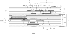
- FIG. 1 is a schematic diagram of a partial structure of film layers of a display assembly according to an embodiment of this application.
- FIG. 2 is a schematic diagram of an optical path of light used for fingerprint detection by the display assembly in a fingerprint recognition phase according to the embodiment in FIG. 1 .
- the display assembly includes a display panel 10 and a fingerprint recognition module 20 located on a light-emitting surface of the display panel 10.
- the light-emitting surface of the display panel 10 is a surface of a side on which the display panel displays a picture.
- the display panel 10 is any one of an organic light emitting display panel, a liquid crystal display panel, or a microdiode display panel.
- FIG. 1 shows only an example in which the display panel is an organic light emitting display panel.
- the display panel 10 includes a substrate 101, an array substrate 102, a display layer 103, and an encapsulation structure 104.
- the light-emitting surface of the display panel 10 is an outer surface of a side that is of the encapsulation structure 104 and that is away from the display layer 103.
- the substrate 101 may be a flexible substrate or a rigid substrate.
- the array substrate 102 includes a plurality of pixel circuits, and only a drive transistor 1021 in the pixel circuit is shown in the figure.
- the display layer 103 includes a pixel definition layer 1031 and a plurality of light emitting components 1032. Only one light emitting component 1032 is shown in the figure.
- the light emitting component 1032 includes an anode 31, a light emitting layer 32, and a cathode 33 that are stacked in sequence.
- the anode 31 is electrically connected to the drive transistor 1021 through a via.
- the encapsulation structure 104 is configured to encapsulate the display layer 103 to isolate water and oxygen, so as to ensure a service life of the light emitting component.
- the encapsulation structure 104 may be rigid encapsulation, and includes an encapsulation cover and a sealant.
- the encapsulation structure 104 may be thin film encapsulation, and includes at least one organic encapsulation layer and at least one inorganic encapsulation layer that are alternately stacked.
- the fingerprint recognition module 20 includes a plurality of fingerprint recognition units, and each fingerprint recognition unit includes at least one phototransistor 1 and one switch transistor 2 connected to the phototransistor 1. Only one fingerprint recognition unit is shown in the figure.
- the phototransistor 1 is used as a photosensitive element, and can convert an optical signal into an electrical signal after receiving fingerprint reflected light in a fingerprint recognition phase.
- the switch transistor 2 is electrically connected to the phototransistor 1.
- the switch transistor 2 is configured to read a fingerprint electrical signal and output the electrical signal to a fingerprint data processing module.
- the fingerprint data processing module performs operation processing on the electrical signal, to generate fingerprint information.
- the phototransistor 1 includes a first active layer 11, a first gate 12, a first source 13, and a first drain 14.
- a material for making the first active layer 11 includes an organic semiconductor material.
- the first drain 14 and the first gate 12 partially overlap to form a first capacitor Cs.
- the organic semiconductor material is any one or more of pentacene (pentacene), 6,13-bis(triisopropylsilanesylacetylene)-pentene (TIPS-pentacene), copper phthalocyanine (CuPc), (dinaphtho[2,3-b:2',3'-flthieno [3,2-b]thiophene) (DNTT), 2,6-bis(methoxyphenyl)anthracene(BOPAnt), poly-3-hexylthiophene(P3HT), poly[bis(3-dodecyl-2-thienyl)-2,2'-dithiophene-5,5'-diyl] (poly[bis(3-dodecyl-2-thienyl)-2,2'-dithiophene-5,5'-diyl], PQT-12), PDVT-10(poly[2,5-bis(alkyl) pyrrolo[
- a film may be coated by using a solution method, and then a pattern of the first active layer 11 is formed by using an etching process.
- the first active layer 11 may alternatively be formed by forming a film by using a deposition method.
- the organic semiconductor material strongly absorbs light.
- the first active layer 11 is used as a light sensing layer. When light irradiates to a surface of the first active layer 11, an electron-hole pair is correspondingly generated inside the first active layer 11 each time a photon is absorbed. Due to an action of an electric field, electrons and holes are separated to generate charge carriers, and the charge carriers migrate inside the material to form a current. This implements converting an optical signal into an electrical signal.
- fingerprint recognition may be implemented by matching a light-sensitive band of an organic semiconductor material with a fingerprint recognition light source.
- the first active layer selects an organic semiconductor material that is sensitive to visible light, for example, an organic semiconductor material that is sensitive to green light, so that a corresponding fingerprint recognition light source emits green light.
- the first active layer selects an organic semiconductor material that is sensitive to infrared light, so that a corresponding fingerprint recognition light source emits infrared light.
- a working state of the phototransistor 1 includes a dark state and an illumination state.
- the dark state of the phototransistor 1 is a state when no light irradiates to the surface of the first active layer 11. In the dark state, when a bias voltage is applied to the phototransistor 1, there is a small leakage current in the first active layer 11.
- the illumination state of the phototransistor 1 is a state when light irradiates to the surface of the first active layer 11. In the illumination state, there is a small leakage current and a photocurrent generated by light excitation in the first active layer 11.
- the switch transistor 2 includes a second active layer 21, a second gate 22, a second source 23, and a second drain 24.
- a material for making the second active layer 21 may be a silicon semiconductor material, such as a monocrystalline silicon semiconductor or a polycrystalline silicon semiconductor, or may be an organic semiconductor material.
- the material for making the second active layer 21 includes any one or more of pentacene, TIPS-pentacene, CuPc, DNTT, BOPAnt, P3HT, PQT-12, PDVT-10, DPP-DTT, 2,7-diocty[1]benzothieno[3,2-B]benzothiophene (C8-BTBT), [4,4,9,9-tetra(4-hexylphenyl)-sbenzodipyridine[1,2-b:5,6-b']dithiophene]-benzothiodiazole copolymer (C16-IDTBT), 2,8-difluoro-5,11-bis(triethylsilylethynyl)anthradithiophene (diF-TES-ADT), 2,9-diphenyl-dinaphtho[2,3-b:2',3'-f]thieno[3,2-b]thiophene (Dph-
- the fingerprint recognition module 20 includes a first metal layer 41.
- the first source 13, the first drain 14, the second source 23, and the second drain 24 are all located at the first metal layer 41, and the first drain 14 is connected to the second source 23.
- the first source 13, the first drain 14, the second source 23, and the second drain 24 may be manufactured in a same etching process, so that complexity of the process may be reduced.
- the first drain 14 and the second source 23 are integrally formed to form a common electrode, one end of the common electrode is used as the first drain 14, and the other end of the common electrode is used as the second source 23.
- the fingerprint recognition module 20 further includes a passivation layer 91 above the first active layer 11 and the second active layer 21.
- the passivation layer 91 may have both insulation and planarization functions.
- the display assembly further includes a protective cover 92 located on the fingerprint recognition module 20.
- the protective cover 92 may be a rigid cover, or may be a flexible cover.
- an anti-impact layer (not shown in the figure) is further disposed between the passivation layer 91 and the protective cover 92. The anti-impact layer can buffer an external force borne by the display assembly, to protect each component in the display assembly from being damaged by the external force.
- a fingerprint recognition light source required for implementing the fingerprint recognition function may be an external light source, for example, a visible light source or an infrared light source.
- the external light source is disposed on a side that is of the display panel and that is away from the fingerprint recognition module.
- a light emitting component on the display panel may be reused as the fingerprint recognition light source.
- FIG. 2 shows only an example in which the light emitting component 1032 is reused as a fingerprint recognition light source. As shown in FIG.
- the light sequentially penetrates through the fingerprint recognition module 20 and the protective cover 92, and then irradiates to a finger 88 of a user.
- the light reflected by the finger penetrates through the protective cover 92 again and then irradiates to the first active layer of the phototransistor 1. After absorbing the fingerprint reflected light, the first active layer converts the optical signal into an electrical signal.
- Fingerprint recognition includes a startup phase, an initial signal reading phase, a fingerprint signal accumulation phase, and a fingerprint signal reading phase.
- the switch transistor 2 and the phototransistor 1 are controlled to be turned off, the phototransistor 1 in the dark state and there is a small leakage current in the phototransistor 1.
- the first capacitor Cs formed between the first drain 14 and the first gate 12 of the phototransistor 1 is charged to accumulate a small amount of initial charge, which is recorded as an amount of initial charge Q0.
- the switch transistor 2 In the initial signal reading phase, when the switch transistor 2 is controlled to be turned on, the second source 23 and the second drain 24 of the switch transistor 2 are connected. Because the first drain 14 is connected to the second source 23, the first capacitor Cs discharges, the amount of initial charge Q0 is read through the second drain 24, and then the switch transistor 2 is controlled to be turned off.
- the phototransistor 1 In the fingerprint signal accumulation phase, after the phototransistor 1 receives the light reflected by the finger, the phototransistor 1 is in an illumination state, and the first active layer 11 is irradiated by the light to generate a charge carrier therein. In this case, a current in the phototransistor 1 increases, and an amount of charge accumulated during charging of the first capacitor Cs increases, which is recorded as an amount of fingerprint charge Q1.
- a fingerprint ridge of the finger is in direct contact with the surface of the display assembly, so that light emitted by the fingerprint recognition light source is received by the phototransistor 1 after being reflected on an interface on which the fingerprint ridge is in contact with the display assembly.
- the fingerprint valley and the fingerprint ridge may be distinguished based on a value of an amount of fingerprint charge.
- the switch transistor 2 In the fingerprint signal reading phase, when the switch transistor 2 is controlled to be turned on, the second source 23 and the second drain 24 of the switch transistor 2 are connected again, the first capacitor Cs discharges, and the amount of fingerprint charge Q1 is read through the second drain 24.
- the amount of initial charge Q0 and the amount of fingerprint charge Q1 are respectively read through the second drain, and the amount of initial charge Q0 and the amount of fingerprint charge Q1 are transferred to the fingerprint data processing module (a module in a system mainboard).
- the fingerprint data processing module collects fingerprint detection signals returned by a plurality of fingerprint recognition units, and performs operation processing, to finally generate fingerprint information.
- the fingerprint recognition module is disposed on the light-emitting surface of the display panel.
- the light reflected by the finger can be received by the fingerprint recognition module without penetrating through a structural film layer of the display panel. This shortens a transmission distance of fingerprint reflected light, and can improve collimation of the fingerprint reflected light, avoid a light loss caused when the fingerprint reflected light penetrates through the structural film layer of the display panel, and improve fingerprint recognition accuracy.
- the phototransistor is used as a photosensitive element in the fingerprint recognition module.
- a structure of the phototransistor is similar to that of the switch transistor.
- the phototransistor and the switch transistor can share at least a part of a making process. This can reduce structure and process complexity of the display assembly, and can also help reduce an overall thickness of the display assembly.
- a light sensing effect (that is, a photosensitive effect) of the photosensitive element is related to an order of magnitude that can be achieved by dividing a photocurrent by a dark current. That is, a larger difference between the photocurrent and the dark current indicates a better light sensing effect and higher sensitivity of fingerprint recognition.
- the dark current is a leakage current of the photosensitive element in the dark state (in a state in which no light irradiates), and the photocurrent is a current generated when the photosensitive element is excited by light in the illumination state (in a state in which light irradiates).
- a photodiode is used as a photosensitive element, and a leakage current of the photodiode in a dark state is at an nA level.
- a light sensing area of the photodiode usually needs to be large, to ensure a light sensing effect of the photodiode. Consequently, a fingerprint recognition module including a switch transistor and a photodiode occupies a large area.
- the fingerprint recognition module When the fingerprint recognition module is disposed on a display surface of a display panel, the fingerprint recognition module greatly shields light emitted from the display panel. This affects a display effect.
- the phototransistor and the switch transistor form the fingerprint recognition unit.
- the leakage current of the phototransistor in the dark state is at a pA level.
- the leakage current of the phototransistor in the dark state is far less than the leakage current of the photodiode in the dark state. Therefore, the phototransistor in this application can have a good light sensing effect even when a size of the phototransistor is small.
- the phototransistor does not shield the light emitted from the display panel as it is disposed on the light-emitting surface of the display panel.
- the fingerprint recognition module 20 further includes a second metal layer 42 and a first insulation layer 51.
- the second metal layer 42 is located on a side that is of the first metal layer 41 and that is close to the display panel 10.
- the first insulation layer 51 is located between the first metal layer 41 and the second metal layer 42.
- the first gate 12 is located at the second metal layer 42. That is, the first gate 12 of the phototransistor 1 is located on a side that is of the first active layer 11 and that is close to the display panel 10, the phototransistor 1 is a transistor of a bottom gate structure, and the first gate 12 does not shield light emitted to the first active layer 11. This ensures that the fingerprint reflected light can be emitted to the first active layer 11 in a fingerprint recognition phase, so that the phototransistor 1 converts an optical signal into an electrical signal.
- the second gate 22 of the switch transistor 2 is also located at the second metal layer 42.
- the second gate 22 of the switch transistor 2 and the first gate 12 of the phototransistor 1 may be made of a same material at a same layer.
- both the switch transistor and the phototransistor are of a bottom gate structure, and the switch transistor and the phototransistor have a same structure, so that the switch transistor and the phototransistor can be manufactured in a same process. This improves fingerprint recognition accuracy, and further reduces structure and process complexity of the display assembly.
- Both the first active layer 11 and the second active layer 21 are located on a side that is of the first insulation layer 51 and that is away from the second metal layer 42, and are in contact with the first insulation layer 51.
- the first insulation layer 51 is manufactured on the first gate 12; then the first metal layer 41 is manufactured on the first insulation layer 51; and the first metal layer 41 is patterned to form the first source 13, the first drain 14, the second source 23, and the second drain 24. Then, the first active layer 11 and the second active layer 21 are manufactured.
- first active layer 11 Two ends of the first active layer 11 are respectively connected to the first source 13 and the first drain 14, and two ends of the second active layer 21 are respectively connected to the second source 23 and the second drain 24. Both the first active layer 11 and the second active layer 21 are in contact with the first insulation layer 51, which is equivalent to that the first active layer 11 and the second active layer 21 are located at a height of a same film layer. This can help reduce a thickness of a film layer of the fingerprint recognition module, and further help reduce an overall thickness of the display assembly.
- the first active layer and the second active layer are made of a same material at a same layer, that is, the pattern of the first active layer and the pattern of the second active layer are formed simultaneously in a same process. This can further simplify the process, and reduce complexity of the process.
- FIG. 3 is another schematic diagram of a partial structure of film layers of a display assembly according to an embodiment of this application.
- the first source 13, the first drain 14, the second source 23, and the second drain 24 are all located at the first metal layer 41.
- the first gate 12 and the second gate 22 are all located at the second metal layer 42.
- the first active layer 11 and the second active layer 21 are made of a same material at a same layer, and are in contact with the first insulation layer 51.
- the fingerprint recognition module 20 further includes a plurality of light shielding parts 61 (only one is shown in the figure), one light shielding part 61 corresponds to one switch transistor 2.
- the light shielding part 61 is located on a side that is of the second active layer 21 and that is away from the display panel 10, and an orthographic projection of the light shielding part 61 on a plane on which the second active layer 21 is located covers the second active layer 21.
- a material for making the light shielding part 61 may be a metal material, an organic light absorbing material, or the like. In practice, a corresponding material may be selected based on a light-sensitive band of an organic semiconductor material used in the first active layer to make the light shielding part. This ensures that the light shielding part shields light of the band.
- the light shielding part can shield light, to prevent the light from irradiating on a surface of the second active layer, so that a carrier inside the second active layer increases. This avoids impact on an on/off status of the switch transistor, and ensures accuracy and performance reliability of fingerprint recognition detection.
- a voltage signal needs to be controlled to pass through the light shielding part 61 at a moment when the switch transistor 1 is turned on, and the light shielding part 61 can be used as a gate of the switch transistor 1. Therefore, the switch transistor 1 forms a transistor of a dual-gate structure, and a turn-on speed of the switch transistor 1 can be increased.
- the passivation layer 91 is disposed above the first active layer 11 and the second active layer 21, and a planarization layer 93 is further disposed above the light shielding part 61.
- the display assembly further includes the protective cover 92.
- an anti-impact layer (not shown) is further disposed on the protective cover 92 and the planarization layer 93.
- both the first active layer and the second active layer are in contact with the first insulation layer, and the second active layer and the first active layer are made of different materials.
- a light-sensitive band of the second active layer is different from a light-sensitive band of the first active layer.
- the fingerprint recognition phase only the first active layer is sensitive to light emitted by the fingerprint recognition light source. Even though irradiating to a surface of the second active layer, fingerprint reflected light is not absorbed by the second active layer to affect the on/off status of the switch transistor.
- no light shielding part needs to be disposed at the second active layer to shield light. This can cancel a process of making the light shielding part.
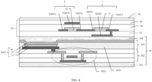
- FIG. 4 is another schematic diagram of a partial structure of film layers of a display assembly according to an embodiment of this application.
- the first source 13, the first drain 14, the second source 23, and the second drain 24 are all located at the first metal layer 41.
- the first gate 12 is located at the second metal layer 42.
- Both the first active layer 11 and the second active layer 21 are located on a side that is of the first insulation layer 51 and that is away from the second metal layer 42, and are in contact with the first insulation layer 51.
- the fingerprint recognition module 20 further includes a third metal layer 43.
- the third metal layer 43 is located on a side that is of the first metal layer 41 and that is away from the display panel 10, and the second gate 22 is located at the third metal layer 43.
- An insulation layer 94 is disposed above the first active layer 11 and the second active layer 21, and a planarization layer 95 is disposed above the second gate 22.
- the protective cover 92 is further disposed on the planarization layer 95.
- the first active layer and the second active layer may be made of a same material at a same layer, so as to ensure that the switch transistor and the phototransistor share a part of the making process. This reduces complexity of the making process.
- the second gate disposed on a side that is of the second active layer and that is away from the display panel can be reused as a light shielding part.
- the second gate can shield light, to prevent fingerprint reflected light from irradiating to a surface of the second active layer, so that a carrier inside the second active layer increases to affect an on/off status of the switch transistor. This ensures accuracy and performance reliability of fingerprint recognition.
- the first source 13 is connected to the first gate 12 through a via 511 on the first insulation layer 51. That is, the first gate 12 and the first source 13 of the phototransistor 1 are connected, so that the phototransistor 1 always works in an off status. In this case, when no light irradiates to a surface of the first active layer 11, a leakage current of the phototransistor 1 is very small. However, in the fingerprint recognition phase, when fingerprint reflected light irradiates to the surface of the first active layer 11, a carrier generated inside the first active layer enables the leakage current of the phototransistor 1 to increase obviously, so that it can be ensured that the phototransistor has high optical sensitivity.
- FIG. 5 is a schematic diagram of a circuit structure of a fingerprint recognition unit in a display assembly according to an embodiment of this application.
- FIG. 6 is a sequence diagram of the fingerprint recognition circuit in the embodiment in FIG. 5 .
- the fingerprint recognition module includes a fingerprint control signal line 71, a fingerprint data signal line 72, and a third voltage signal line 73.
- a second gate of the switch transistor 2 is electrically connected to the fingerprint control signal line 71
- a second drain of the switch transistor 2 is electrically connected to the fingerprint data signal line 72
- both the first gate 12 and the first source 13 are electrically connected to the third voltage signal line 73.
- the switch transistor and the phototransistor in this embodiment of this application may be p-type transistors, or may be n-type transistors, provided that it is ensured that the switch transistor and the phototransistor are of a same type.
- FIG. 7 is a schematic diagram of a circuit structure of a fingerprint recognition module in a display assembly according to an embodiment of this application.
- a plurality of fingerprint recognition units 201 are arranged in an array.
- Each fingerprint recognition unit 201 includes at least one phototransistor 1 and one switch transistor 2. Second gates of the plurality of switch transistors 2 in a same row are electrically connected to one fingerprint control signal line 71, second drains of the plurality of switch transistors 2 in a same column are electrically connected to one fingerprint data signal line 72, and first gates 12 and first sources 13 of the plurality of phototransistors 1 in a same row are electrically connected to one third voltage signal line 73.
- a voltage signal needs to be separately fed into a gate, a source and a drain of the switch transistor, and one electrode of the photodiode, so that a drive circuit is complex.
- a voltage signal needs to be fed into the second gate and the second drain of the switch transistor and the first gate (or the first source) of the phototransistor, so that the drive circuit is simple. Only three types of signal lines need to be disposed in the fingerprint recognition module: the fingerprint control signal line, the fingerprint data signal line, and the third voltage signal line.
- the fingerprint recognition circuit is independent of a circuit that drives the display panel to display, and fingerprint recognition detection does not need to be multiplexed with scanning of one frame of picture in a time division manner. This reduces complexity of a circuit structure.
- the fingerprint control signal line 71 provides a fingerprint control signal Vscan to the switch transistor 2, in this phase, the fingerprint control signal line 71 provides a non-valid level signal to control the switch transistor 2 to be turned off, the fingerprint data signal line 72 feeds a read potential into the second drain of the switch transistor 2, the first source and the first gate of the phototransistor 1 are connected, and the third voltage signal line 73 feeds a bias voltage Vbias.
- the phototransistor 1 is in an off status, that is, in a dark (dark) state, and under an action of a leakage current of the phototransistor 1, the first capacitor Cs starts charging to accumulate a small amount of charge, which is recorded as an amount of initial charge Q0.
- the fingerprint control signal line 71 provides a valid level signal to the switch transistor 2 to control the switch transistor 2 to be turned on.
- the first capacitor Cs discharges, the fingerprint data signal line 72 reads the amount of initial charge Q0 through the second drain 24, and then the fingerprint control signal line 71 provides a non-valid level signal to control the switch transistor 2 to be turned off.
- a fingerprint signal accumulation phase after the phototransistor 1 receives light reflected by a finger, the phototransistor 1 changes from the dark state to an illumination (illumination) state, so that the leakage current of the phototransistor 1 increases. In this case, the amount of charge accumulated during charging of the first capacitor Cs increases, and is recorded as an amount of fingerprint charge Q1.
- the fingerprint control signal line 71 provides a valid level signal to control the switch transistor 2 to be turned on. In this case, the first capacitor Cs discharges, and the fingerprint data signal line 72 reads the amount of fingerprint charge Q1 through the second drain 24.
- the fingerprint data signal line 72 and the second drain are located at a same metal layer, that is, the fingerprint data signal line 72 is located at the first metal layer (refer to a film layer position shown in FIG. 1 ).
- the fingerprint data signal line 72 and the second drain may be manufactured in a same process, and the fingerprint data signal line 72 and the second drain do not need to be connected through a via of an insulation layer.
- the fingerprint control signal line 71 and the second gate are located at a same metal layer, the fingerprint control signal line 71 and the second gate are manufactured in a same making process, and the fingerprint control signal line 71 and the second gate do not need to be connected through a via of an insulation layer. This simplifies the making process.
- the third voltage signal line 73 may be located at a same metal layer as the first gate, or may be located at a same metal layer as the first source.
- the fingerprint data signal line and the second drain are located at the first metal layer
- the fingerprint control signal line and the second gate are located at the third metal layer
- the third voltage signal line and the first gate are located at the second metal layer.
- the fingerprint data signal line, the fingerprint control signal line, and the third voltage signal line are separately wired at three different metal layers. This can reduce wiring density at each metal layer.
- FIG. 8 is another schematic diagram of a partial structure of film layers of a display assembly according to an embodiment of this application.
- the display panel is an organic light emitting display panel.
- the display panel includes a substrate 101, an array substrate 102, a display layer 103, and an encapsulation structure 104 that are sequentially arranged.
- the array substrate 102 includes a gate metal layer 44, a capacitor metal layer (not shown), a source/drain metal layer 45, and a fourth metal layer 46.
- An insulation layer is disposed between two adjacent metal layers.
- a gate 66 of the drive transistor 1021 and a gate scanning line 69 (only shown in the figure) of the display panel are located at the gate metal layer 44.
- a source 67 and a drain 68 of the drive transistor 1021 and a data line of the display panel are located at the source/drain metal layer 45.
- a capacitor plate in the pixel circuit and a reset signal line in the display panel are located at the capacitor metal layer.
- a positive power signal line in the display panel is located at the fourth metal layer 46.
- the second gate 22 of the switch transistor 2 in the fingerprint recognition module 20 is connected to the gate scanning line 69. The figure shows that the second gate 22 is electrically connected to the gate scanning line 69 through at least one connection electrode 461.
- the connection electrode 461 is located at the fourth metal layer 46.
- the second gate 22 is electrically connected to the connection electrode 461 through a via 77 that penetrates through the encapsulation structure 104 and the display layer 103, and the connection electrode 461 is electrically connected to the gate scanning line 69 through a via 78 on the insulation layer.
- the gate scanning line 69 is reused as the fingerprint control signal line, and a control signal is provided to the switch transistor 2 through the gate scanning line 69.
- the second drain 24 of the switch transistor 2 in the fingerprint recognition module may be electrically connected to a data line located at the source/drain metal layer 45, and the data line is reused as a fingerprint data signal line in the fingerprint recognition phase.
- the first gate 12 of the phototransistor 1 in the fingerprint recognition module may be electrically connected to the positive power signal line at the fourth metal layer 46, and the positive power signal line is reused as a third voltage signal line in the fingerprint recognition phase.
- a line that is in the array substrate and that drives the display panel to display is reused as a signal line in the fingerprint recognition module.
- a display drive time sequence and a fingerprint recognition drive time sequence cooperate with each other, so that both a display function and a fingerprint recognition function can be implemented.
- FIG. 9 is another schematic diagram of a partial structure of film layers of a display assembly according to an embodiment of this application.
- FIG. 10 is a schematic diagram of a circuit structure of a fingerprint recognition unit according to an embodiment of FIG. 9 .
- the fingerprint recognition module 20 includes a plurality of fingerprint recognition units.
- Each fingerprint recognition unit includes at least one phototransistor 1 and one switch transistor 2.
- the phototransistor 1 includes a first active layer 11, a first gate 12, a first source 13, and a first drain 14.
- a material for making the first active layer 11 includes an organic semiconductor material.
- the first drain 14 and the first gate 12 partially overlap to form a first capacitor Cs.
- the switch transistor 2 includes a second active layer 21, a second gate 22, a second source 23, and a second drain 24.
- the first drain 14 is connected to the second source 23. Different from the embodiment in FIG. 1 , in the embodiment in FIG. 9 , the first source 13 and the first gate 12 are not connected.
- the fingerprint recognition module includes a fingerprint control signal line 71, a fingerprint data signal line 72, a first voltage signal line 74, and a second voltage signal line 75.
- the second gate is electrically connected to the fingerprint control signal line 71
- the second drain is electrically connected to the fingerprint data signal line 72
- the first gate is electrically connected to the first voltage signal line 74
- the first source is electrically connected to the second voltage signal line 75.
- a voltage supplied by the first voltage signal line 74 to the first gate is greater than a voltage supplied by the second voltage signal line 75 to the first source. Therefore, when the first voltage signal line 74 feeds a voltage signal into the first gate, and the second voltage signal line 75 feeds a voltage signal into the first source, the phototransistor 1 can be controlled to be in an off status.
- a working process of the fingerprint recognition unit may be understood with reference to the foregoing embodiments in FIG. 5 and FIG. 6 , and details are not described herein again.
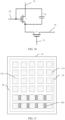
- FIG. 11 is a schematic top view of a partial display assembly according to an embodiment of this application.
- the display panel 10 includes a display area 55 and a non-display area 56, and the display area 55 includes a plurality of pixel areas 111 and a non-pixel area 121 located between adjacent pixel areas 111.
- the pixel area 111 is a pixel light emitting area
- the non-pixel area 121 is a non-light emitting area.
- An organic light emitting display panel is used as an example.
- the pixel area 111 is an area in which a light emitting component is located
- the non-pixel area 121 is an area in which a pixel definition layer spaced from a light emitting component is located.
- a liquid crystal display panel is used as an example.
- the liquid crystal display panel includes a black matrix, and the black matrix includes a plurality of openings.
- An area exposed by the opening is the pixel area 111, and an area between adjacent openings is the non-pixel area.
- An orthographic projection of the fingerprint recognition unit 201 on the display panel 10 is located in the non-pixel area 121.
- An orthographic projection direction of the fingerprint recognition unit 201 towards the display panel 10 is the same as a top-view direction. Therefore, in the top-view direction, the fingerprint recognition unit 201 coincides with an orthographic projection of the fingerprint recognition unit 201 on the display panel 10.
- the fingerprint recognition unit 201 represents an orthographic projection of the fingerprint recognition unit 201 on the display panel 10.
- the fingerprint recognition unit 201 is disposed in only some fixed areas.
- the fingerprint recognition unit may alternatively be disposed on an entire surface of a corresponding display area.
- the fingerprint recognition unit corresponds to a non-pixel area of the display panel. When the display assembly displays, the fingerprint recognition unit does not shield light emission of a pixel area, so that it is ensured that deposition of the fingerprint recognition module does not affect a display effect.
- FIG. 12 is another schematic diagram of a partial structure of film layers of a display assembly according to an embodiment of this application.
- the display panel 10 includes a substrate 101, an array substrate 105, a liquid crystal molecule layer 106, and a color filter substrate 107 that are stacked in sequence.
- the array substrate 105 includes a plurality of pixel circuits. In the figure, only a drive transistor 1051 in the pixel circuit is used as an example.
- the array substrate further includes a pixel electrode 1052 and a common electrode 1053.
- the drive transistor 1051 is connected to the pixel electrode 1052. Relative positions of the pixel electrode 1052 and the common electrode 1053 in the figure may be interchanged.
- the color filter substrate 107 includes a chromatography layer and a black matrix.
- the fingerprint recognition module is located on the display panel.
- the fingerprint recognition module 20 includes a fingerprint recognition unit, and the fingerprint recognition unit includes at least one phototransistor 1 and one switch transistor 2. For a structure of the phototransistor 1 and a structure of the switch transistor 2 in the fingerprint recognition module, refer to the descriptions in any one of the foregoing embodiments. Details are not described herein again.
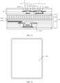
- FIG. 13 is a schematic diagram of a display apparatus according to an embodiment of this application.
- the display apparatus includes the display assembly 100 provided in any embodiment of this application.
- a specific structure of the display assembly 100 has been described in detail in the foregoing embodiment, and details are not described herein again.
- the display apparatus shown in FIG. 13 is merely an example for description.
- the display apparatus may be any electronic device having a fingerprint recognition function, such as a mobile phone, a tablet computer, a notebook computer, an e-book, or a television.
- the display apparatus may be a rigid display apparatus, or may be a flexible or foldable display apparatus.
- a pixel unit on a display panel is reused as a light source for fingerprint recognition in a fingerprint recognition phase.
- the display apparatus includes a fingerprint recognition light source.
- the fingerprint recognition light source is located on a side that is of the display panel and that is away from a fingerprint recognition module.
- the fingerprint recognition light source may be an infrared light source, or may be a visible light source.
Landscapes
- Physics & Mathematics (AREA)
- Engineering & Computer Science (AREA)
- Chemical & Material Sciences (AREA)
- Inorganic Chemistry (AREA)
- Nonlinear Science (AREA)
- General Physics & Mathematics (AREA)
- Microelectronics & Electronic Packaging (AREA)
- Life Sciences & Earth Sciences (AREA)
- Sustainable Development (AREA)
- Theoretical Computer Science (AREA)
- Multimedia (AREA)
- Mathematical Physics (AREA)
- Crystallography & Structural Chemistry (AREA)
- Human Computer Interaction (AREA)
- Optics & Photonics (AREA)
- Image Input (AREA)
- Measurement Of The Respiration, Hearing Ability, Form, And Blood Characteristics Of Living Organisms (AREA)
- Devices For Indicating Variable Information By Combining Individual Elements (AREA)
- Electroluminescent Light Sources (AREA)
- Solid State Image Pick-Up Elements (AREA)
Description
- This application relates to the field of display technologies, and more specifically, to a display assembly, a display apparatus, and a fingerprint recognition method.
- Currently, in-screen optical fingerprint recognition has become a mainstream method for identity recognition of a current electronic device. An optical fingerprint recognition module is disposed on a back side of a substrate of a display panel, and light emitted by a fingerprint recognition light source irradiates to a finger. After being reflected by the finger, the light penetrates through the display panel, and then is received by a photosensitive element, to convert an optical signal into an electrical signal. This implements fingerprint recognition. In a solution in the conventional technology, after light used for fingerprint recognition penetrates through an entire display panel in a thickness direction of the display panel, light loss is large. This seriously affects an amount of light received by the photosensitive element, and further affects accuracy of fingerprint recognition.
-
CN 110 286 796 A discloses a display assembly comprising a display panel and a fingerprint recognition module. - In view of this, this application provides a display assembly, a display apparatus, and a fingerprint recognition method, to resolve a technical problem of low fingerprint recognition accuracy in the conventional technology.
- According to a first aspect, an embodiment of this application provides a display assembly, including a display panel and a fingerprint recognition module located on a light-emitting surface of the display panel. The fingerprint recognition module includes a plurality of fingerprint recognition units, and each fingerprint recognition unit includes at least one phototransistor and one switch transistor.
- The phototransistor includes a first active layer, a first gate, a first source, and a first drain. A material for making the first active layer includes an organic semiconductor material. In a direction perpendicular to the display assembly, the first drain and the first gate partially overlap to form a first capacitor.
- The switch transistor includes a second active layer, a second gate, a second source, and a second drain.
- The fingerprint recognition module includes a first metal layer. The first source, the first drain, the second source, and the second drain are all located at the first metal layer, and the first drain is connected to the second source.
- In this embodiment of this application, the fingerprint recognition module is disposed on the light-emitting surface of the display panel. During fingerprint recognition, light reflected by a finger can be received by the fingerprint recognition module without penetrating through a structural film layer of the display panel. This shortens a transmission distance of fingerprint reflected light, and can improve collimation of the fingerprint reflected light, avoid a light loss caused when the fingerprint reflected light penetrates through the structural film layer of the display panel, and ensure fingerprint recognition accuracy. In addition, the phototransistor is used as a photosensitive element in the fingerprint recognition module. A structure of the phototransistor is similar to that of the switch transistor. During making, the phototransistor and the switch transistor can share at least a part of a making process. This can reduce structure and process complexity of the display assembly, and can also help reduce an overall thickness of the display assembly.
- Further, the fingerprint recognition module further includes a second metal layer and a first insulation layer. The second metal layer is located on a side that is of the first metal layer and that is close to the display panel. The first insulation layer is located between the first metal layer and the second metal layer. The first gate is located at the second metal layer. The phototransistor is a transistor of a bottom gate structure, and the first gate does not shield light emitted to the first active layer. This ensures that the fingerprint reflected light can be emitted to the first active layer in a fingerprint recognition phase, so that the phototransistor converts an optical signal into an electrical signal.
- Further, both the first active layer and the second active layer are located on a side that is of the first insulation layer and that is away from the second metal layer, and are in contact with the first insulation layer. It is equivalent to that the first active layer and the second active layer are located at a height of a same film layer. This can help reduce a thickness of a film layer of the fingerprint recognition module, and further help reduce an overall thickness of the display assembly.
- In an embodiment, the first source is not connected to the first gate, and the fingerprint recognition module includes a fingerprint control signal line, a fingerprint data signal line, a first voltage signal line, and a second voltage signal line. The second gate is electrically connected to the fingerprint control signal line, the second drain is electrically connected to the fingerprint data signal line, the first gate is electrically connected to the first voltage signal line, and the first source is electrically connected to the second voltage signal line. In a fingerprint recognition phase, a voltage supplied by the first voltage signal line to the first gate is greater than a voltage supplied by the second voltage signal line to the first source.
- In an embodiment, the first source is connected to the first gate through a via in the first insulation layer. The first gate and the first source of the phototransistor are connected, so that the phototransistor always works in an off status. In this case, when no light irradiates to a surface of the first active layer, a leakage current of the phototransistor is very small. However, in the fingerprint recognition phase, when the fingerprint reflected light irradiates to the surface of the first active layer, a carrier generated inside the first active layer enables the leakage current of the phototransistor to increase obviously, so that it can be ensured that the phototransistor has high optical sensitivity.
- The fingerprint recognition module includes a fingerprint control signal line, a fingerprint data signal line, and a third voltage signal line.
- The second gate is electrically connected to the fingerprint control signal line, the second drain is electrically connected to the fingerprint data signal line, and both the first gate and the first source are electrically connected to the third voltage signal line. Only three types of signal lines need to be disposed in the fingerprint recognition module: the fingerprint control signal line, the fingerprint data signal line, and the third voltage signal line. This can also simplify a wiring manner in the fingerprint recognition module, and reduce space occupied by wiring.
- Optionally, the second gate is located at the second metal layer. In this case, both the switch transistor and the phototransistor are of a bottom gate structure. The switch transistor and the phototransistor have a same structure, and can be manufactured in a same process. This improves fingerprint recognition accuracy, and further reduces structure and process complexity of the display assembly.
- Optionally, the second active layer and the first active layer are made of a same material at a same layer. Both a pattern of the first active layer and a pattern of the second active layer are formed in a same process, so that the process can be further simplified, and complexity of the process can be reduced.
- Further, the fingerprint recognition module further includes a plurality of light shielding parts. The light shielding part is located on a side that is of the second active layer and that is away from the display panel, and an orthographic projection of the light shielding part on a plane on which the second active layer is located covers the second active layer. When the second active layer and the first active layer are made of the same material at the same layer, the light shielding part can shield light, to prevent the light from irradiating on a surface of the second active layer, so that a carrier inside the second active layer increases. This avoids impact on an on/off status of the switch transistor, and ensures accuracy and performance reliability of fingerprint recognition detection.
- In an embodiment, the fingerprint recognition module further includes a third metal layer. The third metal layer is located on a side that is of the first metal layer and that is away from the display panel, and the second gate is located at the third metal layer. In the fingerprint recognition phase, the second gate disposed on a side that is of the second active layer and that is away from the display panel can be reused as the light shielding part.
- Specifically, the display panel includes a plurality of pixel areas and a non-pixel area located between the adjacent pixel areas. An orthographic projection of the fingerprint recognition unit on the display panel is located in the non-pixel area. During display, the fingerprint recognition unit does not shield light emitted from the pixel area. This ensures that a deposition of the fingerprint recognition module does not affect a display effect.
- Based on a same inventive concept, an embodiment of this application provides a display apparatus, including a display assembly according to any embodiment of this application.
- Based on a same inventive concept, an embodiment of this application provides a fingerprint recognition method, and the fingerprint recognition method is applicable to a display assembly according to any embodiment of this application. The fingerprint recognition method includes:
- controlling both the switch transistor and the phototransistor to be turned off, and charging the first capacitor to accumulate an amount of initial charge under an action of a leakage current of the phototransistor;
- controlling the switch transistor to be turned on, discharging the first capacitor, and controlling the switch transistor to be turned off after reading the amount of initial charge through the second drain;
- after the phototransistor receives light reflected by a finger, increasing the leakage current, and charging the first capacitor to accumulate an amount of fingerprint charge; and
- controlling the switch transistor to be turned on, discharging the first capacitor, and reading the amount of fingerprint charge through the second drain.
- The display assembly, the display apparatus, and the fingerprint recognition method provided in this application have the following beneficial effects: The fingerprint recognition module is disposed on the light-emitting surface of the display panel. During fingerprint recognition, light reflected by a finger can be received by the fingerprint recognition module without penetrating through a structural film layer of the display panel. This shortens a transmission distance of fingerprint reflected light, and can improve collimation of the fingerprint reflected light, avoid a light loss caused when the fingerprint reflected light penetrates through the structural film layer of the display panel, and ensure fingerprint recognition accuracy. In addition, the phototransistor is used as a photosensitive element in the fingerprint recognition module. A structure of the phototransistor is similar to that of the switch transistor. During making, the phototransistor and the switch transistor can share at least a part of a making process. This can reduce structure and process complexity of the display assembly, and can also help reduce an overall thickness of the display assembly.
-
-
FIG. 1 is a schematic diagram of a partial structure of film layers of a display assembly according to an embodiment of this application; -
FIG. 2 is a schematic diagram of an optical path of light used for fingerprint detection by the display assembly in a fingerprint recognition phase according to the embodiment inFIG. 1 ; -
FIG. 3 is another schematic diagram of a partial structure of film layers of a display assembly according to an embodiment of this application; -
FIG. 4 is another schematic diagram of a partial structure of film layers of a display assembly according to an embodiment of this application; -
FIG. 5 is a schematic diagram of a circuit structure of a fingerprint recognition unit in a display assembly according to an embodiment of this application; -
FIG. 6 is a sequence diagram of the fingerprint recognition circuit in the embodiment inFIG. 5 ; -
FIG. 7 is a schematic diagram of a circuit structure of a fingerprint recognition module in a display assembly according to an embodiment of this application; -
FIG. 8 is another schematic diagram of a partial structure of film layers of a display assembly according to an embodiment of this application; -
FIG. 9 is another schematic diagram of a partial structure of film layers of a display assembly according to an embodiment of this application; -
FIG. 10 is a schematic diagram of a circuit structure of a fingerprint recognition unit according to an embodiment ofFIG. 9 ; -
FIG. 11 is a schematic top view of a partial display assembly according to an embodiment of this application; -
FIG. 12 is another schematic diagram of a partial structure of film layers of a display assembly according to an embodiment of this application; and -
FIG. 13 is a schematic diagram of a display apparatus according to an embodiment of this application. - To reduce a light loss caused by light penetrating through a display panel and improve accuracy of fingerprint recognition, the following technical solution is proposed in a related technology: A photosensitive element is integrated into an array substrate of the display panel. During fingerprint recognition, light reflected by a finger can be received by the photosensitive element only by penetrating through an encapsulation structure of the display panel, a light emitting component layer, and some film layers in the array substrate. Alternatively, the photosensitive element is integrated between two adjacent light emitting components, so that light reflected by a finger can be received by the photosensitive element only by penetrating through an encapsulation structure of the display panel and some film layers of a light emitting component layer. Although the foregoing solution can shorten a transmission distance of fingerprint reflected light to some extent, structure and process complexity of the panel is still increased. In addition, the foregoing solution is usually applicable only to an organic light emitting display apparatus.
- Another solution is further proposed in a related technology. A switch transistor and a photosensitive element (a photodiode) that are used for fingerprint recognition are disposed on an encapsulation film of a display panel. Although the transmission distance of the fingerprint reflected light is further shortened, the switch transistor and the photosensitive element have a large difference in structure and making process. In this case, the switch transistor and the photosensitive element need to be separately manufactured. Consequently, complexity of the making process of the panel is increased, and an overall thickness of a fingerprint recognition module including the switch transistor and the photosensitive element is also large.
- Based on the foregoing problem, an embodiment of this application provides a display assembly, which is applicable to any type of display apparatus in the conventional technology, for example, an LCD (liquid crystal display, liquid crystal display), an OLED (organic electroluminesence display, organic electroluminesence display), or a micro LED (micro light emitting diode) display. A phototransistor and a switch transistor are integrated into a fingerprint recognition module and disposed on a light-emitting surface of a display panel, so that fingerprint recognition accuracy can be improved, and structure and process complexity of the display assembly can be reduced.
-
FIG. 1 is a schematic diagram of a partial structure of film layers of a display assembly according to an embodiment of this application.FIG. 2 is a schematic diagram of an optical path of light used for fingerprint detection by the display assembly in a fingerprint recognition phase according to the embodiment inFIG. 1 . - As shown in
FIG. 1 , the display assembly includes adisplay panel 10 and afingerprint recognition module 20 located on a light-emitting surface of thedisplay panel 10. The light-emitting surface of thedisplay panel 10 is a surface of a side on which the display panel displays a picture. Thedisplay panel 10 is any one of an organic light emitting display panel, a liquid crystal display panel, or a microdiode display panel.FIG. 1 shows only an example in which the display panel is an organic light emitting display panel. Thedisplay panel 10 includes asubstrate 101, anarray substrate 102, adisplay layer 103, and anencapsulation structure 104. In this case, the light-emitting surface of thedisplay panel 10 is an outer surface of a side that is of theencapsulation structure 104 and that is away from thedisplay layer 103. Thesubstrate 101 may be a flexible substrate or a rigid substrate. Thearray substrate 102 includes a plurality of pixel circuits, and only adrive transistor 1021 in the pixel circuit is shown in the figure. Thedisplay layer 103 includes apixel definition layer 1031 and a plurality oflight emitting components 1032. Only onelight emitting component 1032 is shown in the figure. Thelight emitting component 1032 includes ananode 31, alight emitting layer 32, and acathode 33 that are stacked in sequence. Theanode 31 is electrically connected to thedrive transistor 1021 through a via. Theencapsulation structure 104 is configured to encapsulate thedisplay layer 103 to isolate water and oxygen, so as to ensure a service life of the light emitting component. Theencapsulation structure 104 may be rigid encapsulation, and includes an encapsulation cover and a sealant. Alternatively, theencapsulation structure 104 may be thin film encapsulation, and includes at least one organic encapsulation layer and at least one inorganic encapsulation layer that are alternately stacked. - The
fingerprint recognition module 20 includes a plurality of fingerprint recognition units, and each fingerprint recognition unit includes at least onephototransistor 1 and oneswitch transistor 2 connected to thephototransistor 1. Only one fingerprint recognition unit is shown in the figure. Thephototransistor 1 is used as a photosensitive element, and can convert an optical signal into an electrical signal after receiving fingerprint reflected light in a fingerprint recognition phase. Theswitch transistor 2 is electrically connected to thephototransistor 1. Theswitch transistor 2 is configured to read a fingerprint electrical signal and output the electrical signal to a fingerprint data processing module. Finally, the fingerprint data processing module performs operation processing on the electrical signal, to generate fingerprint information. - The
phototransistor 1 includes a firstactive layer 11, afirst gate 12, afirst source 13, and afirst drain 14. A material for making the firstactive layer 11 includes an organic semiconductor material. In a direction perpendicular to the display assembly, thefirst drain 14 and thefirst gate 12 partially overlap to form a first capacitor Cs. The organic semiconductor material is any one or more of pentacene (pentacene), 6,13-bis(triisopropylsilanesylacetylene)-pentene (TIPS-pentacene), copper phthalocyanine (CuPc), (dinaphtho[2,3-b:2',3'-flthieno [3,2-b]thiophene) (DNTT), 2,6-bis(methoxyphenyl)anthracene(BOPAnt), poly-3-hexylthiophene(P3HT), poly[bis(3-dodecyl-2-thienyl)-2,2'-dithiophene-5,5'-diyl] (poly[bis(3-dodecyl-2-thienyl)-2,2'-dithiophene-5,5'-diyl], PQT-12), PDVT-10(poly[2,5-bis(alkyl) pyrrolo[3,4-c]-1,4(2H,5H)-dione-alt-5,5'-di(thiophene-2-yl)-2,2'-(E)-2-(2-(thiophen-2-yl)vinyl) thio-phene]), and diketopyrrolo-pyrrole dithienylthieno[3,2-b]thiophene (DPP-DTT). When the firstactive layer 11 is being manufactured, a film may be coated by using a solution method, and then a pattern of the firstactive layer 11 is formed by using an etching process. The firstactive layer 11 may alternatively be formed by forming a film by using a deposition method. The organic semiconductor material strongly absorbs light. The firstactive layer 11 is used as a light sensing layer. When light irradiates to a surface of the firstactive layer 11, an electron-hole pair is correspondingly generated inside the firstactive layer 11 each time a photon is absorbed. Due to an action of an electric field, electrons and holes are separated to generate charge carriers, and the charge carriers migrate inside the material to form a current. This implements converting an optical signal into an electrical signal. Different organic semiconductor materials have different light-sensitive bands. Actually, fingerprint recognition may be implemented by matching a light-sensitive band of an organic semiconductor material with a fingerprint recognition light source. The first active layer selects an organic semiconductor material that is sensitive to visible light, for example, an organic semiconductor material that is sensitive to green light, so that a corresponding fingerprint recognition light source emits green light. Alternatively, the first active layer selects an organic semiconductor material that is sensitive to infrared light, so that a corresponding fingerprint recognition light source emits infrared light. - A working state of the
phototransistor 1 includes a dark state and an illumination state. The dark state of thephototransistor 1 is a state when no light irradiates to the surface of the firstactive layer 11. In the dark state, when a bias voltage is applied to thephototransistor 1, there is a small leakage current in the firstactive layer 11. Correspondingly, the illumination state of thephototransistor 1 is a state when light irradiates to the surface of the firstactive layer 11. In the illumination state, there is a small leakage current and a photocurrent generated by light excitation in the firstactive layer 11. - The
switch transistor 2 includes a secondactive layer 21, asecond gate 22, asecond source 23, and asecond drain 24. A material for making the secondactive layer 21 may be a silicon semiconductor material, such as a monocrystalline silicon semiconductor or a polycrystalline silicon semiconductor, or may be an organic semiconductor material. The material for making the secondactive layer 21 includes any one or more of pentacene, TIPS-pentacene, CuPc, DNTT, BOPAnt, P3HT, PQT-12, PDVT-10, DPP-DTT, 2,7-diocty[1]benzothieno[3,2-B]benzothiophene (C8-BTBT), [4,4,9,9-tetra(4-hexylphenyl)-sbenzodipyridine[1,2-b:5,6-b']dithiophene]-benzothiodiazole copolymer (C16-IDTBT), 2,8-difluoro-5,11-bis(triethylsilylethynyl)anthradithiophene (diF-TES-ADT), 2,9-diphenyl-dinaphtho[2,3-b:2',3'-f]thieno[3,2-b]thiophene (Dph-DNTT). The secondactive layer 21 and the firstactive layer 11 may be made of a same material, or the secondactive layer 21 and the firstactive layer 11 may be made of different materials. - The
fingerprint recognition module 20 includes afirst metal layer 41. Thefirst source 13, thefirst drain 14, thesecond source 23, and thesecond drain 24 are all located at thefirst metal layer 41, and thefirst drain 14 is connected to thesecond source 23. In other words, in a making process of the display assembly, thefirst source 13, thefirst drain 14, thesecond source 23, and thesecond drain 24 may be manufactured in a same etching process, so that complexity of the process may be reduced. Optionally, as shown inFIG. 1 , thefirst drain 14 and thesecond source 23 are integrally formed to form a common electrode, one end of the common electrode is used as thefirst drain 14, and the other end of the common electrode is used as thesecond source 23. - As shown in
FIG. 1 , thefingerprint recognition module 20 further includes apassivation layer 91 above the firstactive layer 11 and the secondactive layer 21. Thepassivation layer 91 may have both insulation and planarization functions. The display assembly further includes aprotective cover 92 located on thefingerprint recognition module 20. Theprotective cover 92 may be a rigid cover, or may be a flexible cover. Optionally, an anti-impact layer (not shown in the figure) is further disposed between thepassivation layer 91 and theprotective cover 92. The anti-impact layer can buffer an external force borne by the display assembly, to protect each component in the display assembly from being damaged by the external force. - The display assembly according to this embodiment of this application can implement a fingerprint recognition function. A fingerprint recognition light source required for implementing the fingerprint recognition function may be an external light source, for example, a visible light source or an infrared light source. During application, the external light source is disposed on a side that is of the display panel and that is away from the fingerprint recognition module. When the display panel is an organic light emitting display panel, a light emitting component on the display panel may be reused as the fingerprint recognition light source.
FIG. 2 shows only an example in which thelight emitting component 1032 is reused as a fingerprint recognition light source. As shown inFIG. 2 , in the fingerprint recognition phase, after light emitted by thelight emitting component 1032 is emitted from the light-emitting surface of thedisplay panel 10, the light sequentially penetrates through thefingerprint recognition module 20 and theprotective cover 92, and then irradiates to afinger 88 of a user. The light reflected by the finger penetrates through theprotective cover 92 again and then irradiates to the first active layer of thephototransistor 1. After absorbing the fingerprint reflected light, the first active layer converts the optical signal into an electrical signal. - In a fingerprint recognition method to which the display assembly according to this embodiment of this application can be applied, a working process of a fingerprint recognition unit is used as an example. Fingerprint recognition includes a startup phase, an initial signal reading phase, a fingerprint signal accumulation phase, and a fingerprint signal reading phase.
- In the startup phase, when the
switch transistor 2 and thephototransistor 1 are controlled to be turned off, thephototransistor 1 in the dark state and there is a small leakage current in thephototransistor 1. In this way, the first capacitor Cs formed between thefirst drain 14 and thefirst gate 12 of thephototransistor 1 is charged to accumulate a small amount of initial charge, which is recorded as an amount of initial charge Q0. - In the initial signal reading phase, when the
switch transistor 2 is controlled to be turned on, thesecond source 23 and thesecond drain 24 of theswitch transistor 2 are connected. Because thefirst drain 14 is connected to thesecond source 23, the first capacitor Cs discharges, the amount of initial charge Q0 is read through thesecond drain 24, and then theswitch transistor 2 is controlled to be turned off. - In the fingerprint signal accumulation phase, after the
phototransistor 1 receives the light reflected by the finger, thephototransistor 1 is in an illumination state, and the firstactive layer 11 is irradiated by the light to generate a charge carrier therein. In this case, a current in thephototransistor 1 increases, and an amount of charge accumulated during charging of the first capacitor Cs increases, which is recorded as an amount of fingerprint charge Q1. When the finger presses a surface of the display assembly, a fingerprint ridge of the finger is in direct contact with the surface of the display assembly, so that light emitted by the fingerprint recognition light source is received by thephototransistor 1 after being reflected on an interface on which the fingerprint ridge is in contact with the display assembly. There is air between a fingerprint valley and the surface of the display assembly, so that light emitted by the fingerprint recognition light source only can be received by thephototransistor 1 after penetrating through an interface between the display assembly and the air, being reflected by the fingerprint valley and then penetrating through the interface between the display assembly and the air again. Therefore, the light reflected by the ridge has light intensity larger than that of the light reflected by the valley. Correspondingly, in the fingerprint signal accumulation phase, a photocurrent generated when the phototransistor receives the light reflected by the ridge is larger than a photocurrent generated when the phototransistor receives the light reflected by the valley. In this case, more charge is accumulated on the first capacitor when the phototransistor receives the light reflected by the ridge. Therefore, in subsequent operation processing, the fingerprint valley and the fingerprint ridge may be distinguished based on a value of an amount of fingerprint charge. - In the fingerprint signal reading phase, when the
switch transistor 2 is controlled to be turned on, thesecond source 23 and thesecond drain 24 of theswitch transistor 2 are connected again, the first capacitor Cs discharges, and the amount of fingerprint charge Q1 is read through thesecond drain 24. - The amount of initial charge Q0 and the amount of fingerprint charge Q1 are respectively read through the second drain, and the amount of initial charge Q0 and the amount of fingerprint charge Q1 are transferred to the fingerprint data processing module (a module in a system mainboard). The fingerprint data processing module collects fingerprint detection signals returned by a plurality of fingerprint recognition units, and performs operation processing, to finally generate fingerprint information.
- According to the display assembly provided in this embodiment of this application, the fingerprint recognition module is disposed on the light-emitting surface of the display panel. During fingerprint recognition, the light reflected by the finger can be received by the fingerprint recognition module without penetrating through a structural film layer of the display panel. This shortens a transmission distance of fingerprint reflected light, and can improve collimation of the fingerprint reflected light, avoid a light loss caused when the fingerprint reflected light penetrates through the structural film layer of the display panel, and improve fingerprint recognition accuracy. In addition, the phototransistor is used as a photosensitive element in the fingerprint recognition module. A structure of the phototransistor is similar to that of the switch transistor. During making, the phototransistor and the switch transistor can share at least a part of a making process. This can reduce structure and process complexity of the display assembly, and can also help reduce an overall thickness of the display assembly.
- In addition, a light sensing effect (that is, a photosensitive effect) of the photosensitive element is related to an order of magnitude that can be achieved by dividing a photocurrent by a dark current. That is, a larger difference between the photocurrent and the dark current indicates a better light sensing effect and higher sensitivity of fingerprint recognition. The dark current is a leakage current of the photosensitive element in the dark state (in a state in which no light irradiates), and the photocurrent is a current generated when the photosensitive element is excited by light in the illumination state (in a state in which light irradiates). In a fingerprint recognition solution in a related technology, a photodiode is used as a photosensitive element, and a leakage current of the photodiode in a dark state is at an nA level. In this case, a light sensing area of the photodiode usually needs to be large, to ensure a light sensing effect of the photodiode. Consequently, a fingerprint recognition module including a switch transistor and a photodiode occupies a large area. When the fingerprint recognition module is disposed on a display surface of a display panel, the fingerprint recognition module greatly shields light emitted from the display panel. This affects a display effect. However, in this embodiment of this application, the phototransistor and the switch transistor form the fingerprint recognition unit. The leakage current of the phototransistor in the dark state is at a pA level. In other words, the leakage current of the phototransistor in the dark state is far less than the leakage current of the photodiode in the dark state. Therefore, the phototransistor in this application can have a good light sensing effect even when a size of the phototransistor is small. The phototransistor does not shield the light emitted from the display panel as it is disposed on the light-emitting surface of the display panel.
- Still refer to
FIG. 1 . Thefingerprint recognition module 20 further includes asecond metal layer 42 and afirst insulation layer 51. Thesecond metal layer 42 is located on a side that is of thefirst metal layer 41 and that is close to thedisplay panel 10. Thefirst insulation layer 51 is located between thefirst metal layer 41 and thesecond metal layer 42. Thefirst gate 12 is located at thesecond metal layer 42. That is, thefirst gate 12 of thephototransistor 1 is located on a side that is of the firstactive layer 11 and that is close to thedisplay panel 10, thephototransistor 1 is a transistor of a bottom gate structure, and thefirst gate 12 does not shield light emitted to the firstactive layer 11. This ensures that the fingerprint reflected light can be emitted to the firstactive layer 11 in a fingerprint recognition phase, so that thephototransistor 1 converts an optical signal into an electrical signal. - In an embodiment, as shown in
FIG. 1 , thesecond gate 22 of theswitch transistor 2 is also located at thesecond metal layer 42. Thesecond gate 22 of theswitch transistor 2 and thefirst gate 12 of thephototransistor 1 may be made of a same material at a same layer. In this embodiment, both the switch transistor and the phototransistor are of a bottom gate structure, and the switch transistor and the phototransistor have a same structure, so that the switch transistor and the phototransistor can be manufactured in a same process. This improves fingerprint recognition accuracy, and further reduces structure and process complexity of the display assembly. - Still refer to
FIG. 1 . Both the firstactive layer 11 and the secondactive layer 21 are located on a side that is of thefirst insulation layer 51 and that is away from thesecond metal layer 42, and are in contact with thefirst insulation layer 51. In a making process, after a patterning process of thefirst gate 12 is completed, thefirst insulation layer 51 is manufactured on thefirst gate 12; then thefirst metal layer 41 is manufactured on thefirst insulation layer 51; and thefirst metal layer 41 is patterned to form thefirst source 13, thefirst drain 14, thesecond source 23, and thesecond drain 24. Then, the firstactive layer 11 and the secondactive layer 21 are manufactured. Two ends of the firstactive layer 11 are respectively connected to thefirst source 13 and thefirst drain 14, and two ends of the secondactive layer 21 are respectively connected to thesecond source 23 and thesecond drain 24. Both the firstactive layer 11 and the secondactive layer 21 are in contact with thefirst insulation layer 51, which is equivalent to that the firstactive layer 11 and the secondactive layer 21 are located at a height of a same film layer. This can help reduce a thickness of a film layer of the fingerprint recognition module, and further help reduce an overall thickness of the display assembly. - In an embodiment, the first active layer and the second active layer are made of a same material at a same layer, that is, the pattern of the first active layer and the pattern of the second active layer are formed simultaneously in a same process. This can further simplify the process, and reduce complexity of the process.
- When the second active layer and the first active layer are made of a same material at a same layer, a light-sensitive band of the second active layer is the same as that of the first active layer. Based on this, to ensure performance reliability of the switch transistor in the fingerprint recognition phase, an embodiment of this application provides another display assembly.
FIG. 3 is another schematic diagram of a partial structure of film layers of a display assembly according to an embodiment of this application. Thefirst source 13, thefirst drain 14, thesecond source 23, and thesecond drain 24 are all located at thefirst metal layer 41. Thefirst gate 12 and thesecond gate 22 are all located at thesecond metal layer 42. The firstactive layer 11 and the secondactive layer 21 are made of a same material at a same layer, and are in contact with thefirst insulation layer 51. Thefingerprint recognition module 20 further includes a plurality of light shielding parts 61 (only one is shown in the figure), onelight shielding part 61 corresponds to oneswitch transistor 2. Thelight shielding part 61 is located on a side that is of the secondactive layer 21 and that is away from thedisplay panel 10, and an orthographic projection of thelight shielding part 61 on a plane on which the secondactive layer 21 is located covers the secondactive layer 21. A material for making thelight shielding part 61 may be a metal material, an organic light absorbing material, or the like. In practice, a corresponding material may be selected based on a light-sensitive band of an organic semiconductor material used in the first active layer to make the light shielding part. This ensures that the light shielding part shields light of the band. The light shielding part can shield light, to prevent the light from irradiating on a surface of the second active layer, so that a carrier inside the second active layer increases. This avoids impact on an on/off status of the switch transistor, and ensures accuracy and performance reliability of fingerprint recognition detection. - Optionally, in the fingerprint recognition phase, a voltage signal needs to be controlled to pass through the
light shielding part 61 at a moment when theswitch transistor 1 is turned on, and thelight shielding part 61 can be used as a gate of theswitch transistor 1. Therefore, theswitch transistor 1 forms a transistor of a dual-gate structure, and a turn-on speed of theswitch transistor 1 can be increased. - In the display assembly according to the embodiment in
FIG. 3 , thepassivation layer 91 is disposed above the firstactive layer 11 and the secondactive layer 21, and aplanarization layer 93 is further disposed above thelight shielding part 61. The display assembly further includes theprotective cover 92. Optionally, an anti-impact layer (not shown) is further disposed on theprotective cover 92 and theplanarization layer 93. - In another embodiment, both the first active layer and the second active layer are in contact with the first insulation layer, and the second active layer and the first active layer are made of different materials. In this case, a light-sensitive band of the second active layer is different from a light-sensitive band of the first active layer. In the fingerprint recognition phase, only the first active layer is sensitive to light emitted by the fingerprint recognition light source. Even though irradiating to a surface of the second active layer, fingerprint reflected light is not absorbed by the second active layer to affect the on/off status of the switch transistor. In this implementation, no light shielding part needs to be disposed at the second active layer to shield light. This can cancel a process of making the light shielding part.
- In another embodiment, the second gate of the switch transistor and the first gate of the phototransistor are located at different metal layers.
FIG. 4 is another schematic diagram of a partial structure of film layers of a display assembly according to an embodiment of this application. Thefirst source 13, thefirst drain 14, thesecond source 23, and thesecond drain 24 are all located at thefirst metal layer 41. Thefirst gate 12 is located at thesecond metal layer 42. Both the firstactive layer 11 and the secondactive layer 21 are located on a side that is of thefirst insulation layer 51 and that is away from thesecond metal layer 42, and are in contact with thefirst insulation layer 51. Thefingerprint recognition module 20 further includes athird metal layer 43. Thethird metal layer 43 is located on a side that is of thefirst metal layer 41 and that is away from thedisplay panel 10, and thesecond gate 22 is located at thethird metal layer 43. Aninsulation layer 94 is disposed above the firstactive layer 11 and the secondactive layer 21, and aplanarization layer 95 is disposed above thesecond gate 22. Theprotective cover 92 is further disposed on theplanarization layer 95. In this implementation, the first active layer and the second active layer may be made of a same material at a same layer, so as to ensure that the switch transistor and the phototransistor share a part of the making process. This reduces complexity of the making process. In addition, in a fingerprint recognition phase, the second gate disposed on a side that is of the second active layer and that is away from the display panel can be reused as a light shielding part. The second gate can shield light, to prevent fingerprint reflected light from irradiating to a surface of the second active layer, so that a carrier inside the second active layer increases to affect an on/off status of the switch transistor. This ensures accuracy and performance reliability of fingerprint recognition. - Still refer to
FIG. 1 . Thefirst source 13 is connected to thefirst gate 12 through a via 511 on thefirst insulation layer 51. That is, thefirst gate 12 and thefirst source 13 of thephototransistor 1 are connected, so that thephototransistor 1 always works in an off status. In this case, when no light irradiates to a surface of the firstactive layer 11, a leakage current of thephototransistor 1 is very small. However, in the fingerprint recognition phase, when fingerprint reflected light irradiates to the surface of the firstactive layer 11, a carrier generated inside the first active layer enables the leakage current of thephototransistor 1 to increase obviously, so that it can be ensured that the phototransistor has high optical sensitivity. -
FIG. 5 is a schematic diagram of a circuit structure of a fingerprint recognition unit in a display assembly according to an embodiment of this application.FIG. 6 is a sequence diagram of the fingerprint recognition circuit in the embodiment inFIG. 5 . As shown inFIG. 5 , the fingerprint recognition module includes a fingerprintcontrol signal line 71, a fingerprintdata signal line 72, and a thirdvoltage signal line 73. A second gate of theswitch transistor 2 is electrically connected to the fingerprintcontrol signal line 71, a second drain of theswitch transistor 2 is electrically connected to the fingerprint data signalline 72, and both thefirst gate 12 and thefirst source 13 are electrically connected to the thirdvoltage signal line 73. It should be noted that the switch transistor and the phototransistor in this embodiment of this application may be p-type transistors, or may be n-type transistors, provided that it is ensured that the switch transistor and the phototransistor are of a same type. - Specifically, a plurality of fingerprint recognition units in the fingerprint recognition module are arranged in an array.
FIG. 7 is a schematic diagram of a circuit structure of a fingerprint recognition module in a display assembly according to an embodiment of this application. A plurality offingerprint recognition units 201 are arranged in an array. Eachfingerprint recognition unit 201 includes at least onephototransistor 1 and oneswitch transistor 2. Second gates of the plurality ofswitch transistors 2 in a same row are electrically connected to one fingerprintcontrol signal line 71, second drains of the plurality ofswitch transistors 2 in a same column are electrically connected to one fingerprint data signalline 72, andfirst gates 12 andfirst sources 13 of the plurality ofphototransistors 1 in a same row are electrically connected to one thirdvoltage signal line 73. - In a related-technology solution in which a fingerprint recognition module includes a switch transistor and a photodiode, to implement a fingerprint recognition function, a voltage signal needs to be separately fed into a gate, a source and a drain of the switch transistor, and one electrode of the photodiode, so that a drive circuit is complex. However, in this embodiment of this application, to implement the fingerprint recognition function, only a voltage signal needs to be fed into the second gate and the second drain of the switch transistor and the first gate (or the first source) of the phototransistor, so that the drive circuit is simple. Only three types of signal lines need to be disposed in the fingerprint recognition module: the fingerprint control signal line, the fingerprint data signal line, and the third voltage signal line. This can also simplify a wiring manner in the fingerprint recognition module, and reduce space occupied by wiring. In addition, the fingerprint recognition circuit is independent of a circuit that drives the display panel to display, and fingerprint recognition detection does not need to be multiplexed with scanning of one frame of picture in a time division manner. This reduces complexity of a circuit structure.
- In a fingerprint recognition process: In a startup phase, the fingerprint
control signal line 71 provides a fingerprint control signal Vscan to theswitch transistor 2, in this phase, the fingerprintcontrol signal line 71 provides a non-valid level signal to control theswitch transistor 2 to be turned off, the fingerprint data signalline 72 feeds a read potential into the second drain of theswitch transistor 2, the first source and the first gate of thephototransistor 1 are connected, and the thirdvoltage signal line 73 feeds a bias voltage Vbias. In this case, thephototransistor 1 is in an off status, that is, in a dark (dark) state, and under an action of a leakage current of thephototransistor 1, the first capacitor Cs starts charging to accumulate a small amount of charge, which is recorded as an amount of initial charge Q0. In an initial signal reading phase, the fingerprintcontrol signal line 71 provides a valid level signal to theswitch transistor 2 to control theswitch transistor 2 to be turned on. In this case, the first capacitor Cs discharges, the fingerprint data signalline 72 reads the amount of initial charge Q0 through thesecond drain 24, and then the fingerprintcontrol signal line 71 provides a non-valid level signal to control theswitch transistor 2 to be turned off. In a fingerprint signal accumulation phase, after thephototransistor 1 receives light reflected by a finger, thephototransistor 1 changes from the dark state to an illumination (illumination) state, so that the leakage current of thephototransistor 1 increases. In this case, the amount of charge accumulated during charging of the first capacitor Cs increases, and is recorded as an amount of fingerprint charge Q1. In a fingerprint signal reading phase, the fingerprintcontrol signal line 71 provides a valid level signal to control theswitch transistor 2 to be turned on. In this case, the first capacitor Cs discharges, and the fingerprint data signalline 72 reads the amount of fingerprint charge Q1 through thesecond drain 24. - Specifically, the fingerprint data signal
line 72 and the second drain are located at a same metal layer, that is, the fingerprint data signalline 72 is located at the first metal layer (refer to a film layer position shown inFIG. 1 ). In this case, the fingerprint data signalline 72 and the second drain may be manufactured in a same process, and the fingerprint data signalline 72 and the second drain do not need to be connected through a via of an insulation layer. This simplifies the process. The fingerprintcontrol signal line 71 and the second gate are located at a same metal layer, the fingerprintcontrol signal line 71 and the second gate are manufactured in a same making process, and the fingerprintcontrol signal line 71 and the second gate do not need to be connected through a via of an insulation layer. This simplifies the making process. In addition, the thirdvoltage signal line 73 may be located at a same metal layer as the first gate, or may be located at a same metal layer as the first source. - In an embodiment, the fingerprint data signal line and the second drain are located at the first metal layer, the fingerprint control signal line and the second gate are located at the third metal layer, and the third voltage signal line and the first gate are located at the second metal layer. The fingerprint data signal line, the fingerprint control signal line, and the third voltage signal line are separately wired at three different metal layers. This can reduce wiring density at each metal layer.
- In another embodiment,
FIG. 8 is another schematic diagram of a partial structure of film layers of a display assembly according to an embodiment of this application. The display panel is an organic light emitting display panel. As shown inFIG. 8 , the display panel includes asubstrate 101, anarray substrate 102, adisplay layer 103, and anencapsulation structure 104 that are sequentially arranged. Thearray substrate 102 includes agate metal layer 44, a capacitor metal layer (not shown), a source/drain metal layer 45, and afourth metal layer 46. An insulation layer is disposed between two adjacent metal layers. Agate 66 of thedrive transistor 1021 and a gate scanning line 69 (only shown in the figure) of the display panel are located at thegate metal layer 44. Asource 67 and adrain 68 of thedrive transistor 1021 and a data line of the display panel are located at the source/drain metal layer 45. A capacitor plate in the pixel circuit and a reset signal line in the display panel are located at the capacitor metal layer. A positive power signal line in the display panel is located at thefourth metal layer 46. Optionally, thesecond gate 22 of theswitch transistor 2 in thefingerprint recognition module 20 is connected to thegate scanning line 69. The figure shows that thesecond gate 22 is electrically connected to thegate scanning line 69 through at least oneconnection electrode 461. Optionally, theconnection electrode 461 is located at thefourth metal layer 46. Thesecond gate 22 is electrically connected to theconnection electrode 461 through a via 77 that penetrates through theencapsulation structure 104 and thedisplay layer 103, and theconnection electrode 461 is electrically connected to thegate scanning line 69 through a via 78 on the insulation layer. In other words, in the fingerprint recognition phase, thegate scanning line 69 is reused as the fingerprint control signal line, and a control signal is provided to theswitch transistor 2 through thegate scanning line 69. In addition, thesecond drain 24 of theswitch transistor 2 in the fingerprint recognition module may be electrically connected to a data line located at the source/drain metal layer 45, and the data line is reused as a fingerprint data signal line in the fingerprint recognition phase. Thefirst gate 12 of thephototransistor 1 in the fingerprint recognition module may be electrically connected to the positive power signal line at thefourth metal layer 46, and the positive power signal line is reused as a third voltage signal line in the fingerprint recognition phase. In this implementation, a line that is in the array substrate and that drives the display panel to display is reused as a signal line in the fingerprint recognition module. A display drive time sequence and a fingerprint recognition drive time sequence cooperate with each other, so that both a display function and a fingerprint recognition function can be implemented. - In another embodiment, the first source and the first gate are not connected, and in the fingerprint recognition phase, the phototransistor is controlled to work in the off status by separately controlling a value of a voltage supplied to the first source and a value of a voltage supplied to the first gate.
FIG. 9 is another schematic diagram of a partial structure of film layers of a display assembly according to an embodiment of this application.FIG. 10 is a schematic diagram of a circuit structure of a fingerprint recognition unit according to an embodiment ofFIG. 9 . - As shown in
FIG. 9 , that thedisplay panel 10 is an organic light emitting display panel is still used as an example, and thefingerprint recognition module 20 is located on the light-emitting surface of thedisplay panel 10. Thefingerprint recognition module 20 includes a plurality of fingerprint recognition units. Each fingerprint recognition unit includes at least onephototransistor 1 and oneswitch transistor 2. Thephototransistor 1 includes a firstactive layer 11, afirst gate 12, afirst source 13, and afirst drain 14. A material for making the firstactive layer 11 includes an organic semiconductor material. Thefirst drain 14 and thefirst gate 12 partially overlap to form a first capacitor Cs. Theswitch transistor 2 includes a secondactive layer 21, asecond gate 22, asecond source 23, and asecond drain 24. Thefirst drain 14 is connected to thesecond source 23. Different from the embodiment inFIG. 1 , in the embodiment inFIG. 9 , thefirst source 13 and thefirst gate 12 are not connected. - As shown in
FIG. 10 , the fingerprint recognition module includes a fingerprintcontrol signal line 71, a fingerprintdata signal line 72, a firstvoltage signal line 74, and a secondvoltage signal line 75. The second gate is electrically connected to the fingerprintcontrol signal line 71, the second drain is electrically connected to the fingerprint data signalline 72, the first gate is electrically connected to the firstvoltage signal line 74, and the first source is electrically connected to the secondvoltage signal line 75. In a fingerprint recognition phase, a voltage supplied by the firstvoltage signal line 74 to the first gate is greater than a voltage supplied by the secondvoltage signal line 75 to the first source. Therefore, when the firstvoltage signal line 74 feeds a voltage signal into the first gate, and the secondvoltage signal line 75 feeds a voltage signal into the first source, thephototransistor 1 can be controlled to be in an off status. - In this implementation, a working process of the fingerprint recognition unit may be understood with reference to the foregoing embodiments in
FIG. 5 and FIG. 6 , and details are not described herein again. - Further,
FIG. 11 is a schematic top view of a partial display assembly according to an embodiment of this application. As shown inFIG. 11 , thedisplay panel 10 includes adisplay area 55 and anon-display area 56, and thedisplay area 55 includes a plurality ofpixel areas 111 and anon-pixel area 121 located betweenadjacent pixel areas 111. Thepixel area 111 is a pixel light emitting area, and thenon-pixel area 121 is a non-light emitting area. An organic light emitting display panel is used as an example. Thepixel area 111 is an area in which a light emitting component is located, and thenon-pixel area 121 is an area in which a pixel definition layer spaced from a light emitting component is located. A liquid crystal display panel is used as an example. The liquid crystal display panel includes a black matrix, and the black matrix includes a plurality of openings. An area exposed by the opening is thepixel area 111, and an area between adjacent openings is the non-pixel area. An orthographic projection of thefingerprint recognition unit 201 on thedisplay panel 10 is located in thenon-pixel area 121. An orthographic projection direction of thefingerprint recognition unit 201 towards thedisplay panel 10 is the same as a top-view direction. Therefore, in the top-view direction, thefingerprint recognition unit 201 coincides with an orthographic projection of thefingerprint recognition unit 201 on thedisplay panel 10. In the top view, thefingerprint recognition unit 201 represents an orthographic projection of thefingerprint recognition unit 201 on thedisplay panel 10.FIG. 11 shows that thefingerprint recognition unit 201 is disposed in only some fixed areas. Optionally, the fingerprint recognition unit may alternatively be disposed on an entire surface of a corresponding display area. In this implementation, the fingerprint recognition unit corresponds to a non-pixel area of the display panel. When the display assembly displays, the fingerprint recognition unit does not shield light emission of a pixel area, so that it is ensured that deposition of the fingerprint recognition module does not affect a display effect. - In all the foregoing embodiments, an example in which the display panel is an organic light emitting display panel is used for description. In the display assembly provided in this embodiment of this application, the display panel may also be a liquid crystal display panel. For details, refer to
FIG. 12. FIG. 12 is another schematic diagram of a partial structure of film layers of a display assembly according to an embodiment of this application. Thedisplay panel 10 includes asubstrate 101, anarray substrate 105, a liquid crystal molecule layer 106, and acolor filter substrate 107 that are stacked in sequence. Thearray substrate 105 includes a plurality of pixel circuits. In the figure, only adrive transistor 1051 in the pixel circuit is used as an example. The array substrate further includes apixel electrode 1052 and acommon electrode 1053. Thedrive transistor 1051 is connected to thepixel electrode 1052. Relative positions of thepixel electrode 1052 and thecommon electrode 1053 in the figure may be interchanged. Thecolor filter substrate 107 includes a chromatography layer and a black matrix. The fingerprint recognition module is located on the display panel. Thefingerprint recognition module 20 includes a fingerprint recognition unit, and the fingerprint recognition unit includes at least onephototransistor 1 and oneswitch transistor 2. For a structure of thephototransistor 1 and a structure of theswitch transistor 2 in the fingerprint recognition module, refer to the descriptions in any one of the foregoing embodiments. Details are not described herein again. - Based on a same inventive concept, an embodiment of this application further provides a display apparatus.
FIG. 13 is a schematic diagram of a display apparatus according to an embodiment of this application. As shown inFIG. 13 , the display apparatus includes thedisplay assembly 100 provided in any embodiment of this application. A specific structure of thedisplay assembly 100 has been described in detail in the foregoing embodiment, and details are not described herein again. Certainly, the display apparatus shown inFIG. 13 is merely an example for description. The display apparatus may be any electronic device having a fingerprint recognition function, such as a mobile phone, a tablet computer, a notebook computer, an e-book, or a television. The display apparatus may be a rigid display apparatus, or may be a flexible or foldable display apparatus. In an embodiment, a pixel unit on a display panel is reused as a light source for fingerprint recognition in a fingerprint recognition phase. In another embodiment, the display apparatus includes a fingerprint recognition light source. The fingerprint recognition light source is located on a side that is of the display panel and that is away from a fingerprint recognition module. The fingerprint recognition light source may be an infrared light source, or may be a visible light source. - The foregoing descriptions are merely specific implementations of the present invention, but are not intended to limit the protection scope of the present invention. Any variation or replacement readily figured out by a person skilled in the art within the technical scope disclosed in the present invention shall fall within the protection scope of the present invention. Therefore, the protection scope of the present invention shall be subject to the protection scope of the claims.
Claims (13)
- A display assembly, comprising a display panel and a fingerprint recognition module located on a light-emitting surface of the display panel, wherein the fingerprint recognition module comprises a plurality of fingerprint recognition units, and each fingerprint recognition unit comprises at least one phototransistor and one switch transistor;the phototransistor comprises a first active layer, a first gate, a first source, and a first drain, a material for making the first active layer comprises an organic semiconductor material, and in a direction perpendicular to the display assembly, the first drain and the first gate partially overlap to form a first capacitor;the switch transistor comprises a second active layer, a second gate, a second source, and a second drain; andthe fingerprint recognition module comprises a first metal layer, wherein the first source, the first drain, the second source, and the second drain are all located at the first metal layer, and the first drain is connected to the second source.
- The display assembly according to claim 1, whereinthe fingerprint recognition module further comprises a second metal layer and a first insulation layer, the second metal layer is located on a side that is of the first metal layer and that is close to the display panel, and the first insulation layer is located between the first metal layer and the second metal layer; andthe first gate is located at the second metal layer.
- The display assembly according to claim 2, wherein
both the first active layer and the second active layer are located on a side that is of the first insulation layer and that is away from the second metal layer, and are in contact with the first insulation layer. - The display assembly according to claim 2, whereinthe fingerprint recognition module comprises a fingerprint control signal line, a fingerprint data signal line, a first voltage signal line, and a second voltage signal line; andthe second gate is electrically connected to the fingerprint control signal line, the second drain is electrically connected to the fingerprint data signal line, the first gate is electrically connected to the first voltage signal line, and the first source is electrically connected to the second voltage signal line, whereinin a fingerprint recognition phase, a voltage supplied by the first voltage signal line to the first gate is greater than a voltage supplied by the second voltage signal line to the first source.
- The display assembly according to claim 2, wherein
the first source is connected to the first gate through a via in the first insulation layer. - The display assembly according to claim 5, whereinthe fingerprint recognition module comprises a fingerprint control signal line, a fingerprint data signal line, and a third voltage signal line; andthe second gate is electrically connected to the fingerprint control signal line, the second drain is electrically connected to the fingerprint data signal line, and both the first gate and the first source are electrically connected to the third voltage signal line.
- The display assembly according to claim 2, wherein
the second gate is located at the second metal layer. - The display assembly according to claim 7, wherein
the second active layer and the first active layer are made of a same material at a same layer. - The display assembly according to claim 8, wherein
the fingerprint recognition module further comprises a plurality of light shielding parts, the light shielding part is located on a side that is of the second active layer and that is away from the display panel, and an orthographic projection of the light shielding part on a plane on which the second active layer is located covers the second active layer. - The display assembly according to claim 2, wherein
the fingerprint recognition module further comprises a third metal layer, the third metal layer is located on a side that is of the first metal layer and that is away from the display panel, and the second gate is located at the third metal layer. - The display assembly according to claim 1, whereinthe display panel comprises a plurality of pixel areas and a non-pixel area located between the adjacent pixel areas; andan orthographic projection of the fingerprint recognition unit on the display panel is located in the non-pixel area.
- A display apparatus, comprising the display assembly according to any one of claims 1 to 11.
- A fingerprint recognition method, applicable to the display assembly according to any one of claims 1 to 11, wherein the fingerprint recognition method comprises:controlling both the switch transistor and the phototransistor to be turned off, and charging the first capacitor to accumulate an amount of initial charge under an action of a leakage current of the phototransistor;controlling the switch transistor to be turned on, discharging the first capacitor, and controlling the switch transistor to be turned off after reading the amount of initial charge through the second drain;after the phototransistor receives light reflected by a finger, increasing the leakage current, and charging the first capacitor to accumulate an amount of fingerprint charge; andcontrolling the switch transistor to be turned on, discharging the first capacitor, and reading the amount of fingerprint charge through the second drain.
Applications Claiming Priority (2)
| Application Number | Priority Date | Filing Date | Title |
|---|---|---|---|
| CN202010246037.8A CN113471249B (en) | 2020-03-31 | 2020-03-31 | Display component, display device and fingerprint recognition method |
| PCT/CN2021/082248 WO2021197118A1 (en) | 2020-03-31 | 2021-03-23 | Display assembly, display device, and fingerprint recognition method |
Publications (3)
| Publication Number | Publication Date |
|---|---|
| EP4116877A1 EP4116877A1 (en) | 2023-01-11 |
| EP4116877A4 EP4116877A4 (en) | 2023-07-26 |
| EP4116877B1 true EP4116877B1 (en) | 2024-07-31 |
Family
ID=77865675
Family Applications (1)
| Application Number | Title | Priority Date | Filing Date |
|---|---|---|---|
| EP21780145.5A Active EP4116877B1 (en) | 2020-03-31 | 2021-03-23 | Display assembly, display device, and fingerprint recognition method |
Country Status (5)
| Country | Link |
|---|---|
| US (1) | US12457866B2 (en) |
| EP (1) | EP4116877B1 (en) |
| JP (1) | JP7407967B2 (en) |
| CN (2) | CN119212488A (en) |
| WO (1) | WO2021197118A1 (en) |
Families Citing this family (8)
| Publication number | Priority date | Publication date | Assignee | Title |
|---|---|---|---|---|
| EP4163818A4 (en) * | 2020-06-09 | 2024-07-03 | Wuhan China Star Optoelectronics Technology Co., Ltd. | Optical fingerprint recognition circuit and display panel |
| CN113990906B (en) * | 2021-10-27 | 2026-01-27 | 京东方科技集团股份有限公司 | Display substrate, line identification method thereof and display device |
| US12471464B2 (en) | 2022-03-30 | 2025-11-11 | Chengdu Boe Optoelectronics Technology Co., Ltd. | Display substrate and display apparatus |
| CN117715464A (en) * | 2022-08-31 | 2024-03-15 | 华为技术有限公司 | Display panel and electronic device |
| CN115909424B (en) * | 2022-11-23 | 2025-10-31 | 武汉华星光电半导体显示技术有限公司 | Display panel |
| KR20250069757A (en) * | 2023-11-10 | 2025-05-20 | 삼성디스플레이 주식회사 | Fingerprint sensor and display device including the same |
| WO2025109913A1 (en) * | 2023-11-20 | 2025-05-30 | ソニーセミコンダクタソリューションズ株式会社 | Semiconductor device and electronic equipment |
| US20260004919A1 (en) * | 2024-06-28 | 2026-01-01 | Teladoc Health, Inc. | Automatic detection of patient availability in a telehealth system |
Family Cites Families (24)
| Publication number | Priority date | Publication date | Assignee | Title |
|---|---|---|---|---|
| KR100873497B1 (en) | 2002-10-17 | 2008-12-15 | 삼성전자주식회사 | Integrated LCD with Fingerprint Recognition Device and Manufacturing Method Thereof |
| JP2007310628A (en) * | 2006-05-18 | 2007-11-29 | Hitachi Displays Ltd | Image display device |
| TWI498786B (en) * | 2009-08-24 | 2015-09-01 | Semiconductor Energy Lab | Touch sensor and method for driving the same and display device |
| US8319299B2 (en) * | 2009-11-20 | 2012-11-27 | Auman Brian C | Thin film transistor compositions, and methods relating thereto |
| WO2011125353A1 (en) * | 2010-04-07 | 2011-10-13 | シャープ株式会社 | Circuit board, display device, and method for manufacturing circuit board |
| JP2015159133A (en) * | 2012-06-14 | 2015-09-03 | シャープ株式会社 | Light receiving device |
| CN104009067A (en) | 2014-06-16 | 2014-08-27 | 信利(惠州)智能显示有限公司 | Organic light-emitting diode display device with touch control function and manufacturing method thereof |
| CN104850292B (en) * | 2015-06-01 | 2017-09-29 | 京东方科技集团股份有限公司 | A kind of In-cell touch panel, its driving method and display device |
| CN105184247B (en) | 2015-08-28 | 2018-12-28 | 京东方科技集团股份有限公司 | A kind of fingerprint recognition element, its recognition methods, display device and display device |
| CN106055162B (en) | 2016-06-30 | 2019-05-03 | 京东方科技集团股份有限公司 | Display components and display devices |
| CN106096595B (en) * | 2016-08-08 | 2022-08-09 | 京东方科技集团股份有限公司 | Fingerprint identification module, manufacturing method thereof and fingerprint identification display device |
| CN106326845B (en) * | 2016-08-15 | 2017-08-11 | 京东方科技集团股份有限公司 | Fingerprint identification unit and preparation method, array base palte, display device and fingerprint identification method |
| CN107885361B (en) | 2016-09-30 | 2022-02-08 | 北京小米移动软件有限公司 | Display device and electronic apparatus |
| KR102675011B1 (en) | 2016-11-28 | 2024-06-17 | 삼성디스플레이 주식회사 | Display device |
| KR102592857B1 (en) * | 2016-12-16 | 2023-10-24 | 삼성디스플레이 주식회사 | Display panel and display device having the same |
| KR101981318B1 (en) * | 2017-04-19 | 2019-05-23 | 크루셜텍(주) | Transparent Fingerprint Image Scanning Panel and Display Apparatus Comprising The Same |
| CN107425041B (en) | 2017-07-27 | 2020-01-31 | 上海天马微电子有限公司 | touch display panel, device and manufacturing method |
| JP2019165129A (en) * | 2018-03-20 | 2019-09-26 | 株式会社ジャパンディスプレイ | Optical sensor device, and display device |
| CN109685003A (en) | 2018-12-24 | 2019-04-26 | 武汉华星光电半导体显示技术有限公司 | OLED display panel and the lower optical finger print recognition methods of screen |
| CN109656048B (en) | 2019-01-10 | 2022-02-15 | 昆山龙腾光电股份有限公司 | Liquid crystal display device having a plurality of pixel electrodes |
| CN109614963B (en) * | 2019-01-28 | 2023-08-29 | 京东方科技集团股份有限公司 | Fingerprint recognition structure and display device |
| CN110008885B (en) | 2019-03-29 | 2021-04-30 | 厦门天马微电子有限公司 | Display panel and display device |
| CN110286796B (en) * | 2019-06-27 | 2023-10-27 | 京东方科技集团股份有限公司 | Electronic substrate and manufacturing method thereof, display panel |
| US20210149249A1 (en) * | 2019-11-19 | 2021-05-20 | Shenzhen China Star Optoelectronics Semiconductor Display Technology Co., Ltd. | Display device |
-
2020
- 2020-03-31 CN CN202411187691.0A patent/CN119212488A/en active Pending
- 2020-03-31 CN CN202010246037.8A patent/CN113471249B/en active Active
-
2021
- 2021-03-23 US US17/915,909 patent/US12457866B2/en active Active
- 2021-03-23 JP JP2022559713A patent/JP7407967B2/en active Active
- 2021-03-23 EP EP21780145.5A patent/EP4116877B1/en active Active
- 2021-03-23 WO PCT/CN2021/082248 patent/WO2021197118A1/en not_active Ceased
Also Published As
| Publication number | Publication date |
|---|---|
| JP7407967B2 (en) | 2024-01-04 |
| EP4116877A4 (en) | 2023-07-26 |
| CN113471249B (en) | 2024-09-20 |
| EP4116877A1 (en) | 2023-01-11 |
| US20230144932A1 (en) | 2023-05-11 |
| JP2023519994A (en) | 2023-05-15 |
| US12457866B2 (en) | 2025-10-28 |
| CN119212488A (en) | 2024-12-27 |
| WO2021197118A1 (en) | 2021-10-07 |
| CN113471249A (en) | 2021-10-01 |
Similar Documents
| Publication | Publication Date | Title |
|---|---|---|
| US12457866B2 (en) | Display assembly, display apparatus, and fingerprint recognition method | |
| EP4113613B1 (en) | Display component, display device, and driving method | |
| CN112055893B (en) | Display panel and manufacturing method thereof | |
| KR101415894B1 (en) | Pixel structure of organic electroluminescence device | |
| US12004385B2 (en) | Display substrate, display panel and display device | |
| CN110164847B (en) | Array substrate, light detection method and assembly and display device | |
| KR20210034552A (en) | Device including image sensor and display screen | |
| JP2010153449A (en) | Light source integrated photoelectric conversion apparatus | |
| US11404469B2 (en) | Flat panel detector and manufacturing method thereof | |
| WO2005093838A1 (en) | Electroluminescent display devices | |
| TWI877138B (en) | Image-sensor matrix-array device comprising thin-film transistors and organic photodiodes | |
| US10770532B2 (en) | Display substrate and method for preparing the same, and display device | |
| CN110164946B (en) | Display substrate, manufacturing method, and display device | |
| KR20000050791A (en) | Thin film transistor type photo sensor | |
| US20240407225A1 (en) | Display apparatus | |
| US20240196688A1 (en) | Display apparatus, display module, and electronic device | |
| US20240188373A1 (en) | Display Substrate, Manufacturing Method Thereof, and Display Apparatus | |
| CN117915723A (en) | Display panel, detection circuit and display device | |
| CN118234303A (en) | Display panel and display terminal | |
| CN116744735A (en) | Display panel, display device and preparation method | |
| JP2008153465A (en) | LIGHT EMITTING DEVICE, ITS MANUFACTURING METHOD, DISPLAY DEVICE USING LIGHT EMITTING DEVICE, OPTICAL HEAD, AND IMAGE FORMING DEVICE | |
| CN117715464A (en) | Display panel and electronic device |
Legal Events
| Date | Code | Title | Description |
|---|---|---|---|
| STAA | Information on the status of an ep patent application or granted ep patent |
Free format text: STATUS: THE INTERNATIONAL PUBLICATION HAS BEEN MADE |
|
| PUAI | Public reference made under article 153(3) epc to a published international application that has entered the european phase |
Free format text: ORIGINAL CODE: 0009012 |
|
| STAA | Information on the status of an ep patent application or granted ep patent |
Free format text: STATUS: REQUEST FOR EXAMINATION WAS MADE |
|
| 17P | Request for examination filed |
Effective date: 20221006 |
|
| AK | Designated contracting states |
Kind code of ref document: A1 Designated state(s): AL AT BE BG CH CY CZ DE DK EE ES FI FR GB GR HR HU IE IS IT LI LT LU LV MC MK MT NL NO PL PT RO RS SE SI SK SM TR |
|
| REG | Reference to a national code |
Ref legal event code: R079 Ref country code: DE Ref document number: 602021016552 Country of ref document: DE Free format text: PREVIOUS MAIN CLASS: G06K0009000000 Ipc: G06V0040130000 |
|
| DAV | Request for validation of the european patent (deleted) | ||
| DAX | Request for extension of the european patent (deleted) | ||
| A4 | Supplementary search report drawn up and despatched |
Effective date: 20230622 |
|
| RIC1 | Information provided on ipc code assigned before grant |
Ipc: G02F 1/13 20060101ALI20230619BHEP Ipc: G06F 3/041 20060101ALI20230619BHEP Ipc: G06V 40/13 20220101AFI20230619BHEP |
|
| GRAP | Despatch of communication of intention to grant a patent |
Free format text: ORIGINAL CODE: EPIDOSNIGR1 |
|
| STAA | Information on the status of an ep patent application or granted ep patent |
Free format text: STATUS: GRANT OF PATENT IS INTENDED |
|
| RIC1 | Information provided on ipc code assigned before grant |
Ipc: H10K 59/60 20230101ALI20240215BHEP Ipc: H10K 59/131 20230101ALI20240215BHEP Ipc: G06F 3/041 20060101ALI20240215BHEP Ipc: G02F 1/13 20060101ALI20240215BHEP Ipc: G06V 40/13 20220101AFI20240215BHEP |
|
| INTG | Intention to grant announced |
Effective date: 20240307 |
|
| RAP3 | Party data changed (applicant data changed or rights of an application transferred) |
Owner name: HUAWEI TECHNOLOGIES CO., LTD. |
|
| P01 | Opt-out of the competence of the unified patent court (upc) registered |
Effective date: 20240514 |
|
| GRAS | Grant fee paid |
Free format text: ORIGINAL CODE: EPIDOSNIGR3 |
|
| GRAA | (expected) grant |
Free format text: ORIGINAL CODE: 0009210 |
|
| STAA | Information on the status of an ep patent application or granted ep patent |
Free format text: STATUS: THE PATENT HAS BEEN GRANTED |
|
| AK | Designated contracting states |
Kind code of ref document: B1 Designated state(s): AL AT BE BG CH CY CZ DE DK EE ES FI FR GB GR HR HU IE IS IT LI LT LU LV MC MK MT NL NO PL PT RO RS SE SI SK SM TR |
|
| REG | Reference to a national code |
Ref country code: CH Ref legal event code: EP Ref country code: GB Ref legal event code: FG4D |
|
| REG | Reference to a national code |
Ref country code: DE Ref legal event code: R096 Ref document number: 602021016552 Country of ref document: DE |
|
| REG | Reference to a national code |
Ref country code: IE Ref legal event code: FG4D |
|
| REG | Reference to a national code |
Ref country code: NL Ref legal event code: FP |
|
| REG | Reference to a national code |
Ref country code: LT Ref legal event code: MG9D |
|
| PG25 | Lapsed in a contracting state [announced via postgrant information from national office to epo] |
Ref country code: PT Free format text: LAPSE BECAUSE OF FAILURE TO SUBMIT A TRANSLATION OF THE DESCRIPTION OR TO PAY THE FEE WITHIN THE PRESCRIBED TIME-LIMIT Effective date: 20241202 |
|
| REG | Reference to a national code |
Ref country code: AT Ref legal event code: MK05 Ref document number: 1709211 Country of ref document: AT Kind code of ref document: T Effective date: 20240731 |
|
| PG25 | Lapsed in a contracting state [announced via postgrant information from national office to epo] |
Ref country code: PT Free format text: LAPSE BECAUSE OF FAILURE TO SUBMIT A TRANSLATION OF THE DESCRIPTION OR TO PAY THE FEE WITHIN THE PRESCRIBED TIME-LIMIT Effective date: 20241202 |
|
| PG25 | Lapsed in a contracting state [announced via postgrant information from national office to epo] |
Ref country code: NO Free format text: LAPSE BECAUSE OF FAILURE TO SUBMIT A TRANSLATION OF THE DESCRIPTION OR TO PAY THE FEE WITHIN THE PRESCRIBED TIME-LIMIT Effective date: 20241031 |
|
| PG25 | Lapsed in a contracting state [announced via postgrant information from national office to epo] |
Ref country code: GR Free format text: LAPSE BECAUSE OF FAILURE TO SUBMIT A TRANSLATION OF THE DESCRIPTION OR TO PAY THE FEE WITHIN THE PRESCRIBED TIME-LIMIT Effective date: 20241101 Ref country code: FI Free format text: LAPSE BECAUSE OF FAILURE TO SUBMIT A TRANSLATION OF THE DESCRIPTION OR TO PAY THE FEE WITHIN THE PRESCRIBED TIME-LIMIT Effective date: 20240731 Ref country code: PL Free format text: LAPSE BECAUSE OF FAILURE TO SUBMIT A TRANSLATION OF THE DESCRIPTION OR TO PAY THE FEE WITHIN THE PRESCRIBED TIME-LIMIT Effective date: 20240731 |
|
| PG25 | Lapsed in a contracting state [announced via postgrant information from national office to epo] |
Ref country code: BG Free format text: LAPSE BECAUSE OF FAILURE TO SUBMIT A TRANSLATION OF THE DESCRIPTION OR TO PAY THE FEE WITHIN THE PRESCRIBED TIME-LIMIT Effective date: 20240731 |
|
| PG25 | Lapsed in a contracting state [announced via postgrant information from national office to epo] |
Ref country code: LV Free format text: LAPSE BECAUSE OF FAILURE TO SUBMIT A TRANSLATION OF THE DESCRIPTION OR TO PAY THE FEE WITHIN THE PRESCRIBED TIME-LIMIT Effective date: 20240731 |
|
| PG25 | Lapsed in a contracting state [announced via postgrant information from national office to epo] |
Ref country code: IS Free format text: LAPSE BECAUSE OF FAILURE TO SUBMIT A TRANSLATION OF THE DESCRIPTION OR TO PAY THE FEE WITHIN THE PRESCRIBED TIME-LIMIT Effective date: 20241130 Ref country code: AT Free format text: LAPSE BECAUSE OF FAILURE TO SUBMIT A TRANSLATION OF THE DESCRIPTION OR TO PAY THE FEE WITHIN THE PRESCRIBED TIME-LIMIT Effective date: 20240731 |
|
| PG25 | Lapsed in a contracting state [announced via postgrant information from national office to epo] |
Ref country code: HR Free format text: LAPSE BECAUSE OF FAILURE TO SUBMIT A TRANSLATION OF THE DESCRIPTION OR TO PAY THE FEE WITHIN THE PRESCRIBED TIME-LIMIT Effective date: 20240731 |
|
| PG25 | Lapsed in a contracting state [announced via postgrant information from national office to epo] |
Ref country code: ES Free format text: LAPSE BECAUSE OF FAILURE TO SUBMIT A TRANSLATION OF THE DESCRIPTION OR TO PAY THE FEE WITHIN THE PRESCRIBED TIME-LIMIT Effective date: 20240731 Ref country code: RS Free format text: LAPSE BECAUSE OF FAILURE TO SUBMIT A TRANSLATION OF THE DESCRIPTION OR TO PAY THE FEE WITHIN THE PRESCRIBED TIME-LIMIT Effective date: 20241031 |
|
| PG25 | Lapsed in a contracting state [announced via postgrant information from national office to epo] |
Ref country code: RS Free format text: LAPSE BECAUSE OF FAILURE TO SUBMIT A TRANSLATION OF THE DESCRIPTION OR TO PAY THE FEE WITHIN THE PRESCRIBED TIME-LIMIT Effective date: 20241031 Ref country code: PL Free format text: LAPSE BECAUSE OF FAILURE TO SUBMIT A TRANSLATION OF THE DESCRIPTION OR TO PAY THE FEE WITHIN THE PRESCRIBED TIME-LIMIT Effective date: 20240731 Ref country code: NO Free format text: LAPSE BECAUSE OF FAILURE TO SUBMIT A TRANSLATION OF THE DESCRIPTION OR TO PAY THE FEE WITHIN THE PRESCRIBED TIME-LIMIT Effective date: 20241031 Ref country code: LV Free format text: LAPSE BECAUSE OF FAILURE TO SUBMIT A TRANSLATION OF THE DESCRIPTION OR TO PAY THE FEE WITHIN THE PRESCRIBED TIME-LIMIT Effective date: 20240731 Ref country code: IS Free format text: LAPSE BECAUSE OF FAILURE TO SUBMIT A TRANSLATION OF THE DESCRIPTION OR TO PAY THE FEE WITHIN THE PRESCRIBED TIME-LIMIT Effective date: 20241130 Ref country code: HR Free format text: LAPSE BECAUSE OF FAILURE TO SUBMIT A TRANSLATION OF THE DESCRIPTION OR TO PAY THE FEE WITHIN THE PRESCRIBED TIME-LIMIT Effective date: 20240731 Ref country code: GR Free format text: LAPSE BECAUSE OF FAILURE TO SUBMIT A TRANSLATION OF THE DESCRIPTION OR TO PAY THE FEE WITHIN THE PRESCRIBED TIME-LIMIT Effective date: 20241101 Ref country code: FI Free format text: LAPSE BECAUSE OF FAILURE TO SUBMIT A TRANSLATION OF THE DESCRIPTION OR TO PAY THE FEE WITHIN THE PRESCRIBED TIME-LIMIT Effective date: 20240731 Ref country code: ES Free format text: LAPSE BECAUSE OF FAILURE TO SUBMIT A TRANSLATION OF THE DESCRIPTION OR TO PAY THE FEE WITHIN THE PRESCRIBED TIME-LIMIT Effective date: 20240731 Ref country code: BG Free format text: LAPSE BECAUSE OF FAILURE TO SUBMIT A TRANSLATION OF THE DESCRIPTION OR TO PAY THE FEE WITHIN THE PRESCRIBED TIME-LIMIT Effective date: 20240731 Ref country code: AT Free format text: LAPSE BECAUSE OF FAILURE TO SUBMIT A TRANSLATION OF THE DESCRIPTION OR TO PAY THE FEE WITHIN THE PRESCRIBED TIME-LIMIT Effective date: 20240731 |
|
| PG25 | Lapsed in a contracting state [announced via postgrant information from national office to epo] |
Ref country code: SM Free format text: LAPSE BECAUSE OF FAILURE TO SUBMIT A TRANSLATION OF THE DESCRIPTION OR TO PAY THE FEE WITHIN THE PRESCRIBED TIME-LIMIT Effective date: 20240731 Ref country code: DK Free format text: LAPSE BECAUSE OF FAILURE TO SUBMIT A TRANSLATION OF THE DESCRIPTION OR TO PAY THE FEE WITHIN THE PRESCRIBED TIME-LIMIT Effective date: 20240731 Ref country code: RO Free format text: LAPSE BECAUSE OF FAILURE TO SUBMIT A TRANSLATION OF THE DESCRIPTION OR TO PAY THE FEE WITHIN THE PRESCRIBED TIME-LIMIT Effective date: 20240731 |
|
| PG25 | Lapsed in a contracting state [announced via postgrant information from national office to epo] |
Ref country code: EE Free format text: LAPSE BECAUSE OF FAILURE TO SUBMIT A TRANSLATION OF THE DESCRIPTION OR TO PAY THE FEE WITHIN THE PRESCRIBED TIME-LIMIT Effective date: 20240731 |
|
| PG25 | Lapsed in a contracting state [announced via postgrant information from national office to epo] |
Ref country code: CZ Free format text: LAPSE BECAUSE OF FAILURE TO SUBMIT A TRANSLATION OF THE DESCRIPTION OR TO PAY THE FEE WITHIN THE PRESCRIBED TIME-LIMIT Effective date: 20240731 |
|
| PG25 | Lapsed in a contracting state [announced via postgrant information from national office to epo] |
Ref country code: IT Free format text: LAPSE BECAUSE OF FAILURE TO SUBMIT A TRANSLATION OF THE DESCRIPTION OR TO PAY THE FEE WITHIN THE PRESCRIBED TIME-LIMIT Effective date: 20240731 Ref country code: SK Free format text: LAPSE BECAUSE OF FAILURE TO SUBMIT A TRANSLATION OF THE DESCRIPTION OR TO PAY THE FEE WITHIN THE PRESCRIBED TIME-LIMIT Effective date: 20240731 |
|
| REG | Reference to a national code |
Ref country code: DE Ref legal event code: R097 Ref document number: 602021016552 Country of ref document: DE |
|
| PLBE | No opposition filed within time limit |
Free format text: ORIGINAL CODE: 0009261 |
|
| STAA | Information on the status of an ep patent application or granted ep patent |
Free format text: STATUS: NO OPPOSITION FILED WITHIN TIME LIMIT |
|
| 26N | No opposition filed |
Effective date: 20250501 |
|
| PG25 | Lapsed in a contracting state [announced via postgrant information from national office to epo] |
Ref country code: SE Free format text: LAPSE BECAUSE OF FAILURE TO SUBMIT A TRANSLATION OF THE DESCRIPTION OR TO PAY THE FEE WITHIN THE PRESCRIBED TIME-LIMIT Effective date: 20240731 |
|
| PG25 | Lapsed in a contracting state [announced via postgrant information from national office to epo] |
Ref country code: MC Free format text: LAPSE BECAUSE OF FAILURE TO SUBMIT A TRANSLATION OF THE DESCRIPTION OR TO PAY THE FEE WITHIN THE PRESCRIBED TIME-LIMIT Effective date: 20240731 |
|
| REG | Reference to a national code |
Ref country code: CH Ref legal event code: H13 Free format text: ST27 STATUS EVENT CODE: U-0-0-H10-H13 (AS PROVIDED BY THE NATIONAL OFFICE) Effective date: 20251024 |
|
| PG25 | Lapsed in a contracting state [announced via postgrant information from national office to epo] |
Ref country code: LU Free format text: LAPSE BECAUSE OF NON-PAYMENT OF DUE FEES Effective date: 20250323 |
|
| REG | Reference to a national code |
Ref country code: BE Ref legal event code: MM Effective date: 20250331 |
|
| PG25 | Lapsed in a contracting state [announced via postgrant information from national office to epo] |
Ref country code: FR Free format text: LAPSE BECAUSE OF NON-PAYMENT OF DUE FEES Effective date: 20250331 |
|
| PG25 | Lapsed in a contracting state [announced via postgrant information from national office to epo] |
Ref country code: BE Free format text: LAPSE BECAUSE OF NON-PAYMENT OF DUE FEES Effective date: 20250331 |
|
| PG25 | Lapsed in a contracting state [announced via postgrant information from national office to epo] |
Ref country code: CH Free format text: LAPSE BECAUSE OF NON-PAYMENT OF DUE FEES Effective date: 20250331 |
|
| PG25 | Lapsed in a contracting state [announced via postgrant information from national office to epo] |
Ref country code: IE Free format text: LAPSE BECAUSE OF NON-PAYMENT OF DUE FEES Effective date: 20250323 |
|
| PGFP | Annual fee paid to national office [announced via postgrant information from national office to epo] |
Ref country code: NL Payment date: 20260213 Year of fee payment: 6 |
|
| PGFP | Annual fee paid to national office [announced via postgrant information from national office to epo] |
Ref country code: GB Payment date: 20260202 Year of fee payment: 6 |
|
| PGFP | Annual fee paid to national office [announced via postgrant information from national office to epo] |
Ref country code: DE Payment date: 20260204 Year of fee payment: 6 |