EP4113815A1 - Control device of a switching voltage regulator and switching voltage regulator - Google Patents
Control device of a switching voltage regulator and switching voltage regulator Download PDFInfo
- Publication number
- EP4113815A1 EP4113815A1 EP22180463.6A EP22180463A EP4113815A1 EP 4113815 A1 EP4113815 A1 EP 4113815A1 EP 22180463 A EP22180463 A EP 22180463A EP 4113815 A1 EP4113815 A1 EP 4113815A1
- Authority
- EP
- European Patent Office
- Prior art keywords
- signal
- switching
- compensation
- control device
- current
- Prior art date
- Legal status (The legal status is an assumption and is not a legal conclusion. Google has not performed a legal analysis and makes no representation as to the accuracy of the status listed.)
- Withdrawn
Links
Images







Classifications
-
- H—ELECTRICITY
- H02—GENERATION; CONVERSION OR DISTRIBUTION OF ELECTRIC POWER
- H02M—APPARATUS FOR CONVERSION BETWEEN AC AND AC, BETWEEN AC AND DC, OR BETWEEN DC AND DC, AND FOR USE WITH MAINS OR SIMILAR POWER SUPPLY SYSTEMS; CONVERSION OF DC OR AC INPUT POWER INTO SURGE OUTPUT POWER; CONTROL OR REGULATION THEREOF
- H02M1/00—Details of apparatus for conversion
- H02M1/08—Circuits specially adapted for the generation of control voltages for semiconductor devices incorporated in static converters
-
- H—ELECTRICITY
- H02—GENERATION; CONVERSION OR DISTRIBUTION OF ELECTRIC POWER
- H02M—APPARATUS FOR CONVERSION BETWEEN AC AND AC, BETWEEN AC AND DC, OR BETWEEN DC AND DC, AND FOR USE WITH MAINS OR SIMILAR POWER SUPPLY SYSTEMS; CONVERSION OF DC OR AC INPUT POWER INTO SURGE OUTPUT POWER; CONTROL OR REGULATION THEREOF
- H02M1/00—Details of apparatus for conversion
- H02M1/0003—Details of control, feedback or regulation circuits
-
- H—ELECTRICITY
- H02—GENERATION; CONVERSION OR DISTRIBUTION OF ELECTRIC POWER
- H02M—APPARATUS FOR CONVERSION BETWEEN AC AND AC, BETWEEN AC AND DC, OR BETWEEN DC AND DC, AND FOR USE WITH MAINS OR SIMILAR POWER SUPPLY SYSTEMS; CONVERSION OF DC OR AC INPUT POWER INTO SURGE OUTPUT POWER; CONTROL OR REGULATION THEREOF
- H02M1/00—Details of apparatus for conversion
- H02M1/0003—Details of control, feedback or regulation circuits
- H02M1/0025—Arrangements for modifying reference values, feedback values or error values in the control loop of a converter
-
- H—ELECTRICITY
- H02—GENERATION; CONVERSION OR DISTRIBUTION OF ELECTRIC POWER
- H02M—APPARATUS FOR CONVERSION BETWEEN AC AND AC, BETWEEN AC AND DC, OR BETWEEN DC AND DC, AND FOR USE WITH MAINS OR SIMILAR POWER SUPPLY SYSTEMS; CONVERSION OF DC OR AC INPUT POWER INTO SURGE OUTPUT POWER; CONTROL OR REGULATION THEREOF
- H02M3/00—Conversion of DC power input into DC power output
- H02M3/02—Conversion of DC power input into DC power output without intermediate conversion into AC
- H02M3/04—Conversion of DC power input into DC power output without intermediate conversion into AC by static converters
- H02M3/10—Conversion of DC power input into DC power output without intermediate conversion into AC by static converters using discharge tubes with control electrode or semiconductor devices with control electrode
- H02M3/145—Conversion of DC power input into DC power output without intermediate conversion into AC by static converters using discharge tubes with control electrode or semiconductor devices with control electrode using devices of a triode or transistor type requiring continuous application of a control signal
- H02M3/155—Conversion of DC power input into DC power output without intermediate conversion into AC by static converters using discharge tubes with control electrode or semiconductor devices with control electrode using devices of a triode or transistor type requiring continuous application of a control signal using semiconductor devices only
- H02M3/156—Conversion of DC power input into DC power output without intermediate conversion into AC by static converters using discharge tubes with control electrode or semiconductor devices with control electrode using devices of a triode or transistor type requiring continuous application of a control signal using semiconductor devices only with automatic control of output voltage or current, e.g. switching regulators
- H02M3/157—Conversion of DC power input into DC power output without intermediate conversion into AC by static converters using discharge tubes with control electrode or semiconductor devices with control electrode using devices of a triode or transistor type requiring continuous application of a control signal using semiconductor devices only with automatic control of output voltage or current, e.g. switching regulators with digital control
-
- H—ELECTRICITY
- H02—GENERATION; CONVERSION OR DISTRIBUTION OF ELECTRIC POWER
- H02M—APPARATUS FOR CONVERSION BETWEEN AC AND AC, BETWEEN AC AND DC, OR BETWEEN DC AND DC, AND FOR USE WITH MAINS OR SIMILAR POWER SUPPLY SYSTEMS; CONVERSION OF DC OR AC INPUT POWER INTO SURGE OUTPUT POWER; CONTROL OR REGULATION THEREOF
- H02M3/00—Conversion of DC power input into DC power output
- H02M3/02—Conversion of DC power input into DC power output without intermediate conversion into AC
- H02M3/04—Conversion of DC power input into DC power output without intermediate conversion into AC by static converters
- H02M3/10—Conversion of DC power input into DC power output without intermediate conversion into AC by static converters using discharge tubes with control electrode or semiconductor devices with control electrode
- H02M3/145—Conversion of DC power input into DC power output without intermediate conversion into AC by static converters using discharge tubes with control electrode or semiconductor devices with control electrode using devices of a triode or transistor type requiring continuous application of a control signal
- H02M3/155—Conversion of DC power input into DC power output without intermediate conversion into AC by static converters using discharge tubes with control electrode or semiconductor devices with control electrode using devices of a triode or transistor type requiring continuous application of a control signal using semiconductor devices only
- H02M3/156—Conversion of DC power input into DC power output without intermediate conversion into AC by static converters using discharge tubes with control electrode or semiconductor devices with control electrode using devices of a triode or transistor type requiring continuous application of a control signal using semiconductor devices only with automatic control of output voltage or current, e.g. switching regulators
- H02M3/158—Conversion of DC power input into DC power output without intermediate conversion into AC by static converters using discharge tubes with control electrode or semiconductor devices with control electrode using devices of a triode or transistor type requiring continuous application of a control signal using semiconductor devices only with automatic control of output voltage or current, e.g. switching regulators including plural semiconductor devices as final control devices for a single load
-
- H—ELECTRICITY
- H02—GENERATION; CONVERSION OR DISTRIBUTION OF ELECTRIC POWER
- H02M—APPARATUS FOR CONVERSION BETWEEN AC AND AC, BETWEEN AC AND DC, OR BETWEEN DC AND DC, AND FOR USE WITH MAINS OR SIMILAR POWER SUPPLY SYSTEMS; CONVERSION OF DC OR AC INPUT POWER INTO SURGE OUTPUT POWER; CONTROL OR REGULATION THEREOF
- H02M3/00—Conversion of DC power input into DC power output
- H02M3/02—Conversion of DC power input into DC power output without intermediate conversion into AC
- H02M3/04—Conversion of DC power input into DC power output without intermediate conversion into AC by static converters
- H02M3/10—Conversion of DC power input into DC power output without intermediate conversion into AC by static converters using discharge tubes with control electrode or semiconductor devices with control electrode
- H02M3/145—Conversion of DC power input into DC power output without intermediate conversion into AC by static converters using discharge tubes with control electrode or semiconductor devices with control electrode using devices of a triode or transistor type requiring continuous application of a control signal
- H02M3/155—Conversion of DC power input into DC power output without intermediate conversion into AC by static converters using discharge tubes with control electrode or semiconductor devices with control electrode using devices of a triode or transistor type requiring continuous application of a control signal using semiconductor devices only
- H02M3/156—Conversion of DC power input into DC power output without intermediate conversion into AC by static converters using discharge tubes with control electrode or semiconductor devices with control electrode using devices of a triode or transistor type requiring continuous application of a control signal using semiconductor devices only with automatic control of output voltage or current, e.g. switching regulators
- H02M3/158—Conversion of DC power input into DC power output without intermediate conversion into AC by static converters using discharge tubes with control electrode or semiconductor devices with control electrode using devices of a triode or transistor type requiring continuous application of a control signal using semiconductor devices only with automatic control of output voltage or current, e.g. switching regulators including plural semiconductor devices as final control devices for a single load
- H02M3/1582—Buck-boost converters
Definitions
- the present invention relates to a control device of a switching voltage regulator and to a switching voltage regulator.
- a switching voltage regulator is able to convert a d.c. input voltage into a d.c. output voltage using different operating schemes and can be obtained using different topologies, one of the most widespread being the four-switch non-inverting topology.
- Figure 1 shows a switching voltage regulator 1 comprising a four-switch non-inverting switching circuit, referred to hereinafter as switching circuit 3, and a control device 5.
- the switching circuit 3 is formed by a first half-bridge 7, a second half-bridge 9 and an inductor 10.
- the first half-bridge 7 is formed by a first high-side switch 11 and a first low-side switch 13, here two N-MOS transistors, coupled in series between an input terminal 15 and a common node 17.
- the common node 17 is coupled to a reference-potential line (ground) 18.
- An input voltage Vin with respect to ground 18 is applied to the input terminal 15.
- the second half-bridge 9 is formed by a second high-side switch 20 and a second low-side switch 22, also here two N-MOS transistors, coupled in series between an output node 24 and the common node 17.
- An output voltage Vout referenced to the ground 18, is present on the output node 24 and is applied to a load 25.
- the inductor 10 is coupled between an intermediate node of the first half-bridge 7 and an intermediate node of the second half-bridge 9.
- the switching voltage regulator 1 can work in one of three operating modes also known as “buck” if Vin > Vout, “boost” if Vin ⁇ Vout and “buck-boost” if Vin ⁇ Vout.
- the operating mode by appropriately controlling switching of the first and the second half-bridges 7, 9, it is in fact possible to cause the output voltage Vout to be maintained at a reference voltage Vref, chosen, for example, by a user according to a specific application, irrespective of the value of the input voltage Vin.
- control device 5 is coupled to the input node 15 and to the output node 24 and receives the reference voltage Vref.
- the control device 5 determines the operating mode of the switching voltage regulator 1 and generates four switch-command signals T1, T2, T3, T4, which command switching, respectively, of the first high-side switch 11, the first low-side switch 13, the second high-side switch 20, and the second low-side switch 22.
- control device 5 forms a loop control circuit configured to measure an error between the output voltage Vout and the reference voltage Vref, generate a correction signal that compensates the error, and modify the switch-command signals T1, T2, T3, T4 so that the output voltage Vout remains equal to the reference voltage Vref.
- control device 5 It is known to design the control device 5 so that the control parameters of the loop control circuit that generate the correction signal are chosen in the design stage irrespective of the operating mode (buck, boost, and buck-boost) of the switching voltage regulator 1, i.e. by finding a trade-off between stability and dynamic performance of the switching voltage regulator 1 that is valid for all operating modes.
- the operating mode buck, boost, and buck-boost
- an approach envisages fixing the control parameters so that the switching voltage regulator 1 is stable in an operating condition critical for the stability of the switching voltage regulator 1.
- the critical operating condition may be in boost mode, when the input voltage Vin has a minimum value and an output current, for instance through the load 25, has a maximum value.
- the switching voltage regulator 1 In fact, optimising the loop control circuit so that the switching voltage regulator 1 is stable in the critical operating condition causes the switching voltage regulator 1 to have poor performance in the other operating modes. For instance, in this case, the switching voltage regulator 1 will have, in buck mode, a bandwidth narrower than what it would be possible to obtain without at the same time jeopardising the stability thereof.
- the aim of the present invention is to overcome the disadvantages of the prior art.
- a control device of a switching voltage regulator and a switching voltage regulator are provided, as defined in the annexed claims.
- FIG. 2 shows a block diagram of an electronic apparatus 50 comprising a switching voltage regulator 52, also referred to hereinafter simply as regulator 52, a memory 54 and a load 58, coupled together.
- a switching voltage regulator 52 also referred to hereinafter simply as regulator 52
- memory 54 and a load 58, coupled together.
- the regulator 52 receives an input voltage Vin and a reference voltage Vref and supplies an output voltage Vout to the load 58.
- the reference voltage Vref indicates a desired value of the output voltage Vout and is chosen by a user of the electronic apparatus 50, for example in an initialisation step of the electronic apparatus 50.
- the reference voltage Vref received by the regulator 52 is here of an analog type. However, the regulator 52 can also receive a digital value of the reference voltage Vref and convert it internally into a voltage of an analog type by a dedicated digital-to-analog converter (DAC) (not illustrated).
- DAC digital-to-analog converter
- the memory 54 stores a plurality of configuration parameters, as described in detail hereinafter, and provides to the regulator 52 a configuration signal CONF indicative of the configuration parameters.
- the electronic apparatus 50 may also comprise a control unit 500 (represented by a dashed line in Figure 2 ), coupled to the regulator 52.
- the control unit 500 may be integrated in a same die with the regulator 52 or may be integrated in a different die.
- the regulator 52 comprises a switching circuit and a control device designated, respectively, by 60 and 62 in the case of a current-control mode, described with reference to Figures 4-9 , and by 305 and 310 in the case of a voltage-control mode, described with reference to Figure 12 .
- the switching circuit 60, 305 and the control device 62, 310 may be integrated in a same die or formed in different dice.
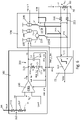
- the switching circuit 60 illustrated in detail in Figure 4 , is here a four-switch non-inverting circuit, in particular configured to operate in buck, boost, and buck-boost mode, according to whether the input voltage Vin is, respectively, higher, lower, and approximately equal to the output voltage Vout (or to the reference voltage Vref).
- the switching circuit 60 is formed by a first half-bridge 64 and a second half-bridge 65.
- the first half-bridge 64 is formed by a first high-side switch 68 and a first low-side switch 69, here two N-MOS transistors, coupled in series between an input node 70 and a common node 72.
- the first high-side switch 68 is coupled between the input node 70 and an intermediate node 74 of the first half-bridge 64
- the first low-side switch 69 is coupled between the intermediate node 74 of the first half-bridge 64 and the common node 72.
- the input node 70 receives the input voltage Vin with respect to a reference-potential line (ground) 78.
- the regulator 52 is configured to operate in current-control mode; consequently, the common node 72 is coupled to the ground 78 by a sense resistor 80 having a resistance Rs.
- the second half-bridge 65 is formed by a second high-side switch 82 and a second low-side switch 83, which also here are two N-MOS transistors, coupled in series between an output node 84 and the common node 72.
- the second high-side switch 82 is coupled between the output node 84 and an intermediate node 85 of the second half-bridge 65
- the second low-side switch 83 is coupled between the intermediate node 85 of the second half-bridge 65 and the common node 72.
- the output node 84 supplies the output voltage Vout, with respect to ground the 78.
- the switching circuit 61 also comprises an inductor 87 having an inductance L and coupled between the intermediate node 74 of the first half-bridge 64 and the intermediate node 85 of the second half-bridge 65.
- control device 62 is coupled to the output node 84 and to the input node 70 and further receives the configuration signal CONF and the reference voltage Vref.
- control device 62 is also coupled to the sense resistor 80, from which it receives a signal indicating the current I L that flows through the inductor 87.
- the control device 62 supplies a first switch-command signal T1, a second switch-command signal T2, a third switch-command signal T3, and a fourth switch-command signal T4 to the switching circuit 60.
- the first, second, third, and fourth switch-command signals T1, T2, T3, T4 control switching, respectively, of the first high-side switch 68, the first low-side switch 69, the second high-side switch 82, and the second low-side switch 83, according to whether the regulator 52 is in the buck, boost, or buck-boost operating modes.
- the third switch-command signal T3 maintains the second high-side switch 82 in a closed or ON state (i.e., enabling a passage of current), whereas the fourth switch-command signal T4 maintains the second low-side switch 83 in an open or OFF state (i.e., blocking the passage of current).
- the first and the second switch-command signals T1, T2 each have a square waveform such that a first step and a second step of current-flow are obtained.
- the first switch-command signal T1 closes the first high-side switch 68, and the second switch-command signal T2 opens the first low-side switch 69. Consequently, a current (indicated by a dashed arrow I L1 in Figure 4 ) may flow from the input node 70 to the output node 84 through the first high-side switch 68, the inductor 87, and the second high-side switch 82.
- the first switch-command signal T1 opens the first high-side switch 68, and the second switch-command signal T2 closes the first low-side switch 69. Consequently, a current (indicated by a dashed-and-dotted arrow I L2 in Figure 4 ) may flow from the ground 78 to the output node 84 through the sense resistor 80, the first low-side switch 69, the inductor 87, and the second high-side switch 82.
- the first switch-command signal T1 maintains the first high-side switch 68 closed, while the second switch-command signal T2 maintains the first low-side switch 69 open.
- the third and the fourth switch-command signals T3, T4 each have a square waveform such that a third and a fourth current-flow steps are obtained.
- the third switch-command signal T3 closes the second high-side switch 82, and the fourth switch-command signal T4 opens the second low-side switch 83. Consequently, a current (once again indicated by the dashed arrow I L1 in Figure 4 ) may flow from the input node 70 to the output node 84 through the first high-side switch 68, the inductor 87, and the second high-side switch 82.
- the third switch-command signal T3 opens the second high-side switch 82, and the fourth switch-command signal T4 closes the second low-side switch 83. Consequently, a current (indicated by a dotted arrow I L3 in Figure 4 ) may flow from the input node 70 to the ground 78 through the first high-side switch 68, the inductor 87, the second low-side switch 83, and the sense resistor 80.
- the first, the second, the third, and the fourth switch-command signals T1, T2, T3, T4 may be controlled so as to alternate a current-flow step of the buck mode with a current-flow step of the boost mode.
- the first switch-command signal T1 may be the same as the fourth switch-command signal T4
- the third switch-command signal T3 may be the same as the second switch-command signal T2 so as to obtain a fifth current-flow step and a sixth current-flow step.
- the fifth current-flow step may be the same as the second current-flow step, where a current (indicated once again by the dashed-and-dotted arrow I L2 in Figure 4 ) may flow from the ground 78 to the output node 84 through the sense resistor 80, the first low-side switch 69, the inductor 87, and the second high-side switch 82.
- the sixth current-flow step may be the same as the fourth current-flow step, where a current (indicated once again by the dotted arrow I L3 in Figure 4 ) may flow from the input node 70 to the ground 78 through the first high-side switch 68, the inductor 87, the second low-side switch 83, and the sense resistor 80.
- the switch-command signals T1-T4 may be driven so as to obtain also a seventh current-flow step, which is the same as the first and the third current-flow steps, wherein a current (indicated once again by the dashed arrow I L1 in Figure 4 ) may flow from the input node 70 to the output node 84 through the first high-side switch 68, the inductor 87, and the second high-side switch 82.
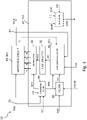
- control device 62 comprises a mode-determining module 89, a control loop circuit 91, a pulse modulator 92 and a driving logic circuit 94.
- the mode-determining module 89 is coupled to the input node 70 and to the output node 84 of the regulator 52 and comprises two mode comparators 95A, 95B.
- the input voltage Vin is coupled to the non-inverting input of the mode comparators 95A, 95B by a voltage divider including a plurality of resistors, here three resistors 96.
- the output voltage Vout is coupled to the inverting input of the mode comparators 95A, 95B by a voltage divider including a plurality of resistors, here two resistors 97.
- the mode comparators 95A, 95B each generate a respective output logic signal O1, O2, which is a function of the difference between the input voltage Vin and the output voltage Vout.
- the resistors 96, 97 and the mode comparators 95A, 95B are designed in such a way that the output logic signals O1, O2 switch when the difference between the output voltage Vout and the input voltage Vin is equal to a first buck-boost threshold Vth1 or to a second buck-boost threshold Vth2.
- the output logic signals O1, O2 of the mode comparators 95A, 95B are supplied to a verification logic module 98, which compares the output logic signals O1, O2 and generates a mode signal MOD indicative of the current operating mode (buck, boost, or buck-boost) of the regulator 52.
- the verification logic module 98 may set the buck-boost operating mode as the current operating mode. If (Vin - Vout) > Vth2, then the verification logic module 98 may set the buck operating mode as the current operating mode. If (Vin - Vout) ⁇ Vth1, then the verification logic module 98 may set the boost operating mode as the current operating mode.
- the control device 62 further comprises a register 99 (illustrated in detail in Figure 5 ), which receives the configuration signal CONF from the memory 54, for example in a start-up step of the electronic apparatus 50, and stores the configuration parameters.
- the configuration signal CONF is indicative of a plurality of control parameters PAR_1, ..., PAR_N useful for control of the regulator 52, as described in detail hereinafter.
- the configuration signal CONF indicates, for each control parameter PAR_i of the plurality of control parameters PAR_1, ..., Par_N, at least two values, at least one of which is associated with the buck operating mode and at least one of which is associated with the boost operating mode.
- the register 99 receives the mode signal MOD and generates a control parameters signal PAR.
- the control parameters signal PAR indicates, for each control parameter PAR_i, one of the values of the control parameter PAR_i stored in the register 99 and associated with the current operating mode.
- the control device 62 also comprises a diagnosis unit 510 (represented by a dashed line in Figure 3 ) configured to generate a diagnosis signal DIAG indicative of a specific operating condition of the regulator 52.
- the diagnosis signal DIAG is supplied to the control unit 500.
- the control unit 500 processes the diagnosis signal DIAG and supplies a plurality of control signals CONT to the regulator 52, in particular to the register 99, indicative of the desired values of the control parameters PAR_i.
- control unit 500 determines, as a function of the specific operating condition, the values of the control parameters PAR stored in the register 99 that optimise the performance of the regulator 52 and therefore to be provided to the control loop circuit 91.
- the diagnosis unit 510 may comprise a circuit for measuring the current that flows through the load 58.
- the diagnosis signal DIAG may indicate a measured value of the load current.
- the control signal CONT may indicate a specific value of each control parameter PAR_i stored in the register 99.
- diagnosis unit 510 may comprise a circuit configured to provide an accurate measurement of the output voltage Vout and/or of the input voltage Vin of the switching circuit 60.
- the control unit 500 through the control signal CONT, may thus select the values of the control parameters PAR_i not only as a function of the ratio between the input voltage Vin and the output voltage Vout, but also as a function of just the value of the input voltage Vin and/or of the output voltage Vout.
- control loop circuit 91 comprises a compensation circuit 100, a current detector 103 and a correction circuit 106.
- the compensation circuit 100 generates a compensation signal Vc as a function of the control parameters signal PAR and of a difference V E between the output voltage Vout and the reference voltage Vref.
- the current detector 103 is coupled to the sense resistor 80 and generates a current-sense signal Vcs associated with the inductor current I L .
- the correction circuit 106 receives the compensation signal Vc and the current-sense signal Vcs and calculates the difference thereof to generate a differential signal DIFF, supplied to the pulse modulator 92, at input to a comparator 107.
- the comparator 107 from the differential signal DIFF, generates a pulse-width-modulated signal PWM, supplied to the driving logic circuit 94 ( Figure 3 ) that generates, in a known way, for example, as described above, the first, the second, the third, and the fourth switch-command signals T1, T2, T3, T4 for driving the switching circuit 60.
- the compensation circuit 100 ( Figure 6 ) comprises an operational transconductance amplifier (OTA) 110 having a variable gain gm and receiving at input the reference voltage Vref and a feedback voltage FB.
- OTA operational transconductance amplifier
- the feedback voltage FB is a fraction of the output voltage Vout.
- the feedback voltage FB is obtained by a feedback voltage divider 112 here comprising two resistors 113, 114 arranged in series between the ground 78 and the output node 84.
- the compensation circuit 100 further comprises a variable compensation network 116 coupled between the ground 78 and the output 115 of the OTA 110 and generating the compensation signal Vc, referred to hereinafter also as compensation voltage.
- variable compensation network 116 is here of the second order and is formed by a first compensation capacitor 123 having a variable capacitance C1 and coupled in parallel with a series circuit formed by a compensation resistor 118, having a variable resistance Rc, and a second compensation capacitor 121, having a variable capacitance C2.
- control parameters signal PAR comprises a first signal PAR_gm that commands the variation of the value of the variable gain gm of the OTA 110, a second signal PAR_C1 that commands the variation of the value of the variable capacitance C1 of the first compensation capacitor 123, a third signal PAR_C2 that commands the variation of the value of the variable capacitance C2 of the second compensation capacitor 121, and a fourth signal PAR_Rc that commands the variation of the value of the variable resistance Rc of the compensation resistor 118.
- Figure 7 shows an embodiment of the variable compensation network 116.
- the compensation resistor 118 is coupled between the output 115 of the OTA 110 and a resistor terminal 125 and is formed by a first resistor 126 and a plurality of selectable resistors, here a first selectable resistor 127A, a second selectable resistor 127B and a third selectable resistor 127C, arranged in series.
- the selectable resistors 127A-127C are each formed by a resistor 130 and a resistor switch 132 arranged in parallel with respect to one another.
- the resistors 130 may have a same value of resistance or a different value, which can be determined in the design stage according to the specific application.
- the resistor switches 132 are here each formed by an N-MOS transistor and a P-MOS transistor having source and drain terminals coupled together and receiving, respectively, the fourth signal PAR_Rc of the control parameters signal PAR and a negated value thereof.
- the fourth signal PAR_Rc of the control parameters signal PAR comprises a plurality of pairs of complementary bits, one for each selectable resistor 127A-127C.
- the fourth signal PAR_Rc of the control parameters signal PAR comprises a first pair of complementary bits (selr0, selr0_n) for the first selectable resistor 127A, a second pair of complementary bits (selr1, selr1_n) for the second selectable resistor 127B, and a third pair of complementary bits (selr2, selr2_n) for the third selectable resistor 127C.
- the resistor switch 132 of the first selectable resistor 127A is closed and forms a short-circuit in parallel to the respective resistor 130. If moreover, once again by way of example, both the second pair and the third pair of complementary bits (selr0, selr0_n) have the value (0,1), then both the resistor switch 132 of the second selectable resistor 127B and the resistor switch 132 of the third selectable resistor 127C are open.
- part of the error current I E flows through the first resistor 126 and through the resistor 130 of the second and the third selectable resistors 127B, 127C. Accordingly, the resistance Rc of the compensation resistor 118 is given by the sum of the resistances of the first resistor 126, the resistor 130 of the second selectable resistor 127B and the resistor 130 of the third selectable resistor 127C.
- the compensation resistor 118 may have, in use, up to a maximum of eight different values, as a function of the resistance value of the resistors 126, 130 and of the number of selectable resistors 127A-127C activated.
- the second compensation capacitor 121 is coupled between the resistor terminal 125 and the ground 78 and is formed by a first capacitor 135 and a plurality of selectable capacitors, here a first selectable capacitor 136A, a second selectable capacitor 136B and a third selectable capacitor 136C, arranged in parallel to one another.
- the selectable capacitors 136A-136C of the second compensation capacitor 121 are each formed by a capacitor 137 and a capacitor switch 139 coupled in series.
- the capacitors 137 of the selectable capacitors 136A-136C of the second compensation capacitor 121 may have a same value of capacitance or a different value, which can be determined in the design stage according to the specific application.
- the capacitor switches 139 of the selectable capacitors 136A-136C of the second compensation capacitor 121 are here each formed by an N-MOS transistor, whose switching is controlled by the third signal PAR_C2 of the control parameters signal PAR.
- the third signal PAR_C2 of the control parameters signal PAR here comprises three bits, one for each selectable capacitor 136A-136C of the second compensation capacitor 121.
- the third signal PAR_C2 of the control parameters signal PAR comprises a first bit sel0, a second bit sell and a third bit sel2, respectively, for the first, the second, and the third selectable capacitors 136A, 136B, 136C of the second compensation capacitor 121.
- the capacitor switch 139 of the first selectable capacitor 136A of the second compensation capacitor 121 is closed and couples the respective capacitor 137 to the ground 78. If moreover, once again by way of example, the second and the third bits sell, sel2 have the value '0', then the respective capacitor switches 139 are open.
- part of the error current I E flows between the resistor node 125 and the ground 78 through the first capacitor 135 and the first selectable capacitor 136A of the second compensation capacitor 121. Accordingly, the variable capacitance C2 of the second compensation capacitor 121 is given by the sum of the capacitances of the respective first capacitor 135 and of the respective first selectable capacitor 136A.
- the second compensation capacitor 121 may have, in use, up to a maximum of eight different values as a function of the value of capacitance of the respective capacitors 135, 137 and of the number of respective selectable capacitors 136A-136C activated.
- the first compensation capacitor 123 is coupled between the output 115 of the OTA 110 and the ground 78 and is formed by a first capacitor 143 and a plurality of selectable capacitors, here a first selectable capacitor 145A, a second selectable capacitor 145B, and a third selectable capacitor 145C, coupled in parallel to one another.
- the selectable capacitors 145A-145C of the first compensation capacitor 123 are each formed by a capacitor 146 and a capacitor switch 147 coupled together in series.
- the capacitors 146 of the selectable capacitors 145A-145C of the first compensation capacitor 123 can have a same value of capacitance or a different value, which can be determined in the design stage according to the specific application.
- the capacitor switches 147 of the first compensation capacitor 123 are here each formed by an N-MOS transistor, whose switching is controlled by the second signal PAR_C1 of the control parameters signal PAR.
- the second signal PAR_C1 of the control parameters signal PAR here comprises three bits, one for each selectable capacitor 145A-145C of the first compensation capacitor 123.
- the second signal PAR_C1 of the control parameters signal PAR comprises a first bit selc0, a second bit selc1 and a third bit selc2, respectively, for the first, the second and the third selectable capacitors 145A, 145B, 145C of the first compensation capacitor 123.
- the capacitor switch 147 of the first selectable capacitor 145A of the first compensation capacitor 123 is closed and couples the respective capacitor 146 to the ground 78. If moreover, once again by way of example, the second and the third bits selc1, selc2 have the value '0', then the respective capacitor switches 147 are open.
- part of the error current I E flows between the output 115 of the OTA 110 and the ground 78 through the first capacitor 143 and the first selectable capacitor 145A of the first compensation capacitor 123. Accordingly, the variable capacitance C1 of the first compensation capacitor 123 is given by the sum of the capacitances of the respective first capacitor 143 and the respective first selectable capacitor 145A.
- the first compensation capacitor 123 may have, in use, up to a maximum of eight different values as a function of the value of capacitance of the respective capacitors 143, 146 and of the number of respective selectable capacitors 145A-145C activated.
- Figure 8 shows a circuit diagram of an embodiment of the OTA 110.
- the OTA 110 is a single-stage amplifier obtained with MOSFET transistors.
- the OTA 110 has an input stage 150 and an output stage 152 coupled between a supply node 155 and the ground 78.
- the input stage 150 is formed by a first input transistor 156A and a second input transistor 156B, here MOSFET transistors of a P type, which receive at input the feedback voltage FB and, respectively, the reference voltage Vref.
- the first and the second input transistors 156A, 156B have source terminals coupled together and to a source node 157, which is coupled to the supply node 155 by a tail current source 158.
- the input transistors 156A, 156B moreover have drain terminals coupled to the ground 78 through a first tail transistor 159A and, respectively, a second tail transistor 159B.
- the tail current source 158 is here formed by a first current source 158A and a second current source 158B, wherein the first current source 158A is fixed and the second current source 158B comprises a source switch 160 in series.
- the source switch 160 enables to activate or deactivate, in use, the second current source 158B.
- the source switch 160 may be selectively opened or closed as a function of the mode signal MOD.
- the current supplied by the tail current source 158 may therefore be chosen as a function of the operating mode of the regulator 52.
- the output stage 152 has a configuration of the cascode type and is here formed by a first high-side mirror portion 162A and a second high-side mirror portion 162B, here two MOSFET transistors of a P type, and a first low-side mirror portion 164A and a second low-side mirror portion 164B coupled, respectively, to the first tail transistor 159A and to the second tail transistor 159B.
- the first and the second low-side mirror portions 164A, 164B have a variable mirror factor that may be selected as a function of the first signal PAR_gm of the control parameters signal PAR.
- first and the second low-side mirror portions 164A, 164B are each formed by a fixed transistor 166 and a plurality of selectable transistors, here a first selectable transistor 167A and a second selectable transistor 167B of an N-MOS type.
- the first and the second low-side mirror portions 164A, 164B each comprise a first transistor switch 169A and a second transistor switch 169B connected in series, respectively, to the first and the second selectable transistors 167A, 167B.
- the first signal PAR_gm of the control parameters signal PAR comprises, in the embodiment illustrated, two bits s0, s1, whose values control the switching of the first transistor switch 169A and of the second transistor switch 169B, respectively.
- the first signal PAR_gm of the control parameters signal PAR modifies the mirror factor of the first and the second low-side mirror portions 164A, 164B.
- the gain gm of the OTA 110 may be modified, in use, as a function of the operating mode of the regulator 52.
- the compensation circuit 100 supplies the compensation voltage Vc to the correction circuit 106.
- the correction circuit 106 comprises a compensation current source 180, which generates a control current Ioc as a function of the compensation voltage Vc.
- the compensation voltage Vc generates a compensation current Ic in the compensation-current source 180.
- the control current Ioc supplied by the compensation current source 180 is equal to the compensation current Ic. If, instead, the compensation current Ic is higher than the limit current value I_lim, then the control current Ioc is equal to the limit current value I_lim.
- control parameters signal PAR also comprises a fifth signal PAR_Ilim, which sets the limit current value I_lim.
- Figure 9 shows an embodiment of the compensation current source 180, here obtained using MOSFET transistors, comprising an input transistor 183 having a gate terminal coupled to the control voltage Vc and a source terminal coupled to the ground 78 through a resistor 185.
- the compensation current Ic which is a function of the compensation voltage Vc, therefore flows through the input transistor 183 of the compensation-current source 180.
- the compensation current source 180 comprises a current-mirror portion 186 and a current-limiting portion 188, configured to set the limit current value I_lim, i.e., a maximum current value that may be mirrored at output by the compensation-current source 180.
- the current-mirror portion 186 is formed by an input mirror branch 186A coupled to the input transistor 183, an intermediate mirror branch 186B coupled in series to the current-limiting portion 188, and an output mirror branch 186C that supplies the control current Ioc at output from the compensation current source 180.
- the intermediate mirror branch 186B is coupled in series to the current-limiting portion 188.
- the current-limiting portion 188 has a variable mirror factor that may be selected as a function of the fifth signal PAR_Ilim of the control parameters signal PAR.
- the current-limiting portion 188 is formed by a fixed transistor 189, a plurality of limitation transistors, here a first limiting transistor 190A, a second limiting transistor 190B, and a third limiting transistor 190C of an N-MOS type, and a mirror portion 193 that controls switching-on of the first, the second, and the third limiting transistors 190A, 190B, 190C.
- the current-limiting portion 188 comprises a plurality of limiting switches, one for each limiting transistor 190A-190C; in particular, here, a first limiting switch 195A, a second limiting switch 195B, and a third limiting switch 195C connected in series, respectively, to the first, the second, and the third limiting transistors 190A-190C.
- the fifth signal PAR_Ilim of the control parameters signal PAR comprises, in the embodiment illustrated, three bits sI0, sI1, sI2, whose values control switching of the first, the second, and the third limiting switches 195A, 195B, 195C, respectively.
- the fifth signal PAR_Ilim of the control parameters signal PAR modifies the mirror factor of the current-limiting portion 188, and thus determines the maximum current value I_lim that the compensation-current source 180 may supply at output.
- the correction circuit 106 also comprises a slope-current source 200 and an offset-current source 205.
- the slope-current source 200 generates a current Islope that is added in a sum node 210 to the control current Ioc supplied by the compensation-current source 180.
- the current Islope may be determined, in a known way, as a function of a difference between the input voltage Vin and the output voltage Vout and is useful, for example, in applications in which the regulator 52 operates at a fixed frequency, for damping the onset of sub-harmonic oscillations.
- the offset-current source 205 generates a variable offset current I_off, whose value may be modified by a sixth signal PAR_Ioff of the control parameters signal PAR.
- the selectable values of the offset current I_off are chosen in the design stage and are useful for setting a maximum value of current that can flow in the inductor 87.
- the offset current I_off may determine a maximum negative current value in the inductor 87, i.e., that flows from the intermediate node 85 of the second half-bridge 65 to the intermediate node 74 of the first half-bridge 74 ( Figure 4 ).
- the correction circuit 106 provides the differential signal DIFF between a first input node 215 and a second input node 216 of the comparator 107, which in turn generates the pulse-width-modulated signal PWM.
- the correction circuit 106 also comprises a first input resistor 220, which has a resistance Rth and is coupled between the first input node 215 of the comparator 107 and the common node 72, and a second input resistor 221, which has a resistance Rth and is coupled between the second input node 216 of the comparator 107 and the ground 78.
- the resistance Rth of the first and the second input resistors 220, 221 is much higher than the resistance Rs of the sense resistor 80.
- the resistance Rth may be of the order of kiloohms and the resistance Rs of the order of milliohms.
- the output of the sum node 210 and the output of the offset-current source 205 are coupled to the first input node 215 or the second input node 216 of the comparator 107 by a respective switch 225A, 225B, according to the current operating mode of the regulator 52.
- the output of the sum node 210 is coupled to the first input node 215 of the comparator 107, and the output of the offset-current source 205 is coupled to the second input node 216 of the comparator 107.
- control current Ioc and the slope current Islope may flow to the ground 78 through the first input resistor 220, and the detection resistance 80 and the offset current Ioff may flow to the ground 78 through the second input resistor 221.
- the pulse modulator 107 is configured to be triggered when I L ⁇ [(Ioc + Islope) - Ioff] ⁇ Rth/Rs.
- the output of the sum node 210 is coupled to the second input node 216 of the comparator 107, and the output of the offset-current source 205 is coupled to the first input node 215 of the comparator 107.
- the offset current Ioff may flow to the ground 78 through the first input resistor 220 and the sense resistance 80, and the control current Ioc and the slope current Islope may flow to the ground 78 through the second input resistor 221.
- the pulse modulator 107 is configured to be triggered when I L > [(Ioc + Islope) - Ioff] ⁇ Rth/Rs.
- the driving logic circuit 94 generates, in a known way, from the pulse-width-modulated signal PWM, the four switch-command signals T1, T2, T3, T4 for switching appropriately the first and the second half-bridges 64, 65 of the switching circuit 60.
- control loop circuit 91 in particular of the compensation circuit 100, enables to modify, in use, a transfer function of the control loop circuit 91. Consequently, by modifying the transfer function of the control loop circuit 91, it is possible to optimise the performance of the regulator 52 in each operating mode.
- the values of the control parameters stored in the register 99 may be chosen, in the design stage, so as to guarantee high stability and excellent dynamic performance, for example a large bandwidth, of the regulator 52, irrespective of the current operating mode of the regulator 52.
- the configurability of the value of the limit current I_lim at output from the compensation-current source 180 makes it possible to guarantee an optimised protection from overload in any operating mode of the regulator 52.
- the compensation network 116 forms a second-order compensator.
- the compensation network may also be a compensator of a different order, according to the specific application.
- FIG 10 shows a different embodiment of the compensation circuit, here designated again by 100, wherein the compensation network, here designated by 250, is of the first order.
- the compensation network 250 is formed by just one compensation capacitor 251 coupled between the output 115 and the ground 78.
- the compensation capacitor 251 has a variable capacitance, whose value may be controlled by a signal PAR_C' of the control parameters signal PAR.
- the value of capacitance of the compensation capacitor 251 may be modified in a way similar to what has been illustrated in Figure 7 for the first compensation capacitor 123.
- FIG 11 shows another embodiment of the compensation circuit, once again here designated by 100, wherein the compensation network, here designated by 254, is of the third order.
- the compensation network 254 is formed by an output sub-network, which is the same as the compensation network 116 of Figure 6 and is consequently designated once again by 116, and a variable input sub-network 256.
- variable input sub-network 256 is coupled between the output node 84 of the regulator 52, at the output voltage Vout, and an intermediate node of the feedback voltage divider 112, between the first and the second input resistors 113, 114.
- the input sub-network 256 is coupled in parallel to the first input resistor 113 and is formed by an input compensation resistor 258 having a resistance R" and an input compensation capacitor 259 having a capacitance C", coupled together in series.
- both the capacitance C" of the input compensation capacitor 259 and the resistance R" of the input compensation resistor 258 are variable and controlled, respectively, by a signal PAR_C" and a signal PAR_R" of the control parameters signal PAR.
- the capacitance C" of the input compensation capacitor 259 and the resistance R" of the input compensation resistor 258 may be modified in a way similar to what has been illustrated in Figure 7 for the compensation resistor 118 and the second compensation capacitor 121.
- Figure 12 shows a different embodiment of the regulator 52 comprising the switching circuit 305 and the control device 310 (illustrated only in part in Figure 12 ).
- control device 310 also here comprises ( Figure 3 ) the operating-mode determination module 89, the driving logic circuit 94, the register 99 and ( Figure 10 ) the pulse-modulation circuit 92 and a control loop circuit, designated by 315.
- the switching circuit 305 has a general structure similar to the switching circuit 60 of Figure 4 ; consequently, elements in common are designated by the same reference numbers and are not described any further herein.
- the switching circuit 305 differs from the switching circuit 60 in that the common node 72 is directly coupled to the ground 78.
- the regulator 52 has a voltage-control mode; consequently, the sense resistor 80 of Figure 4 is not present in the switching circuit 305.
- the control loop circuit 315 comprises a compensation circuit 320, which generates the compensation voltage Vc from the difference between the output voltage Vout and the reference voltage Vref, and a ramp-generator module 325, which generates a periodic reference signal Vr, in particular a saw-tooth signal.
- the compensation voltage Vc and the periodic reference signal Vr are supplied at input to the pulse modulator 67, from which the comparator 107 can generate, in a known way, the pulse-width-modulated signal PWM.
- control parameters of the compensation circuit 320 are variable, in use, as a function of the control parameters signal PAR and of the mode signal MOD.
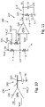
- Figure 13 shows an embodiment of the compensation circuit 320 comprising an operational amplifier 322 having a gain Av, and a variable compensation network, here designated by 324.
- the gain Av of the operational amplifier 322 is fixed.
- the value of the gain Av of the operational amplifier 322 may be variable. For instance, it may be controlled, in use, by a signal PAR_Av (represented by a dashed arrow in Figure 13 ) of the control parameters signal PAR, for example in a way similar to what has been illustrated for the OTA 110 in Figure 8 .
- the operational amplifier 322 has an inverting input at the feedback voltage FB, a non-inverting input at the reference voltage Vref, and an output node 326 at the compensation voltage Vc.
- variable compensation network 324 is of the first type and is formed by just one compensation capacitor, here designated by 328, which has a capacitance C'v and is coupled between the inverting input and the output node 326 of the operational amplifier 322.
- the value of the capacitance C'v of the compensation capacitor 328 is controlled, in use, by a signal PAR_C'v of the control parameters signal PAR, for instance in a way similar to what has been illustrated in Figure 7 and here not described any further.
- FIG 14 shows a different embodiment of the compensation network 324 of Figure 13 , here designated by 330.
- the compensation network 330 is of the second order and also comprises a compensation sub-network 332 coupled between the output node 326 and the inverting input of the operational amplifier 322, in parallel to the compensation capacitor 328.
- the compensation sub-network 332 is formed by a resistor 334 having a variable resistance Rv and a capacitor 335 having a variable capacitance C"v, coupled in series.
- the variable capacitance C"v of the capacitor 335 and the resistance Rv of the resistor 334 are controlled, in use, by a signal PAR_C"v and a signal PAR_Rv, respectively, of the control parameters signal PAR, for instance in a way similar to what has been illustrated in Figure 7 and here not described any further.
- FIG 15 shows a further embodiment of the compensation network 330 of Figure 14 , here designated by 340.
- the compensation network 340 is of the third order and also comprises an input sub-network 342 coupled between the output node 84 of the regulator 52 and the inverting input of the operational amplifier 322.
- the input sub-network 342 is formed by a resistor 344 having a variable resistance R'v and a capacitor 345 having a variable capacitance C′′′v, coupled in series.
- the variable capacitance C′′′v of the capacitor 345 and the resistance R'v of the resistor 344 are controlled, in use, by a signal PAR_C′′′v and a signal PAR_R′v, respectively, of the control parameters signal PAR, for example in a way similar to what has been illustrated in Figure 7 and here not described any further.
- the configurability of the compensation circuit 320 makes it possible to optimise the performance of the regulator 52 of Figure 12 in each operating mode, also in a voltage-control mode.
- the compensation circuit 320 of Figures 13 , 14, and 15 may be used also in the current-control mode, in place of the compensation circuit 100 of Figures 6 , 10, and 11 .
- the compensation circuit 100 of Figures 6 , 10, and 11 may also be used in the voltage-control mode, in place of the compensation circuit 320 of Figures 13 , 14, and 15 .
- the operating-mode determination module may determine the operating mode of the regulator 52 by comparing the input voltage Vin with the reference voltage Vref.
- the compensation network 116 may be obtained in a way different from what has been illustrated in Figure 7 .
- Figure 17 shows a different embodiment of the compensation network 116 of Figure 7 , here designated by 600.
- the compensation network 600 has the same structure as the compensation network 116 and further comprises a buffer 605 having an input node in common with the output 115 of the OTA 110 and, at output, a charge node 610.
- the capacitors 146 of the selectable capacitors 145A-145C of the first compensation capacitor 123, and the capacitors 137 of the selectable capacitors 136A-136C of the second compensation capacitor 121 are coupled between the ground 78 and the charge node 610.
- the buffer 605 maintains the compensation voltage Vc across the capacitors 146 of the selectable capacitors 145A-145C of the first compensation capacitor 123 and the capacitors 137 of the selectable capacitors 136A-136C of the second compensation capacitor 121.
Landscapes
- Engineering & Computer Science (AREA)
- Power Engineering (AREA)
- Dc-Dc Converters (AREA)
- Details Of Television Scanning (AREA)
- Control Of Eletrric Generators (AREA)
Abstract
Description
- The present invention relates to a control device of a switching voltage regulator and to a switching voltage regulator.
- As is known, a switching voltage regulator is able to convert a d.c. input voltage into a d.c. output voltage using different operating schemes and can be obtained using different topologies, one of the most widespread being the four-switch non-inverting topology.
-
Figure 1 shows aswitching voltage regulator 1 comprising a four-switch non-inverting switching circuit, referred to hereinafter asswitching circuit 3, and acontrol device 5. - The
switching circuit 3 is formed by a first half-bridge 7, a second half-bridge 9 and aninductor 10. - The first half-
bridge 7 is formed by a first high-side switch 11 and a first low-side switch 13, here two N-MOS transistors, coupled in series between aninput terminal 15 and acommon node 17. - The
common node 17 is coupled to a reference-potential line (ground) 18. - An input voltage Vin with respect to
ground 18 is applied to theinput terminal 15. - The second half-
bridge 9 is formed by a second high-side switch 20 and a second low-side switch 22, also here two N-MOS transistors, coupled in series between anoutput node 24 and thecommon node 17. - An output voltage Vout, referenced to the
ground 18, is present on theoutput node 24 and is applied to aload 25. - The
inductor 10 is coupled between an intermediate node of the first half-bridge 7 and an intermediate node of the second half-bridge 9. - As a function of the ratio between the input voltage Vin and the output voltage Vout, the
switching voltage regulator 1 can work in one of three operating modes also known as "buck" if Vin > Vout, "boost" if Vin < Vout and "buck-boost" if Vin ≈ Vout. - According to the operating mode, by appropriately controlling switching of the first and the second half-
bridges - For this purpose, the
control device 5 is coupled to theinput node 15 and to theoutput node 24 and receives the reference voltage Vref. - From the input voltage Vin, the output voltage Vout and the reference voltage Vref, the
control device 5 determines the operating mode of theswitching voltage regulator 1 and generates four switch-command signals T1, T2, T3, T4, which command switching, respectively, of the first high-side switch 11, the first low-side switch 13, the second high-side switch 20, and the second low-side switch 22. - In detail, the
control device 5 forms a loop control circuit configured to measure an error between the output voltage Vout and the reference voltage Vref, generate a correction signal that compensates the error, and modify the switch-command signals T1, T2, T3, T4 so that the output voltage Vout remains equal to the reference voltage Vref. - It is known to design the
control device 5 so that the control parameters of the loop control circuit that generate the correction signal are chosen in the design stage irrespective of the operating mode (buck, boost, and buck-boost) of theswitching voltage regulator 1, i.e. by finding a trade-off between stability and dynamic performance of theswitching voltage regulator 1 that is valid for all operating modes. - For instance, an approach envisages fixing the control parameters so that the
switching voltage regulator 1 is stable in an operating condition critical for the stability of theswitching voltage regulator 1. - For example, the critical operating condition may be in boost mode, when the input voltage Vin has a minimum value and an output current, for instance through the
load 25, has a maximum value. - However, the above approach has disadvantages.
- In fact, optimising the loop control circuit so that the
switching voltage regulator 1 is stable in the critical operating condition causes theswitching voltage regulator 1 to have poor performance in the other operating modes. For instance, in this case, theswitching voltage regulator 1 will have, in buck mode, a bandwidth narrower than what it would be possible to obtain without at the same time jeopardising the stability thereof. - The aim of the present invention is to overcome the disadvantages of the prior art.
- According to the present invention, a control device of a switching voltage regulator and a switching voltage regulator are provided, as defined in the annexed claims.
- For a better understanding of the present invention, some embodiments thereof are now described, purely by way of non-limiting example, with reference to the attached drawings, wherein:
-
Figure 1 shows a block diagram of a known switching voltage regulator; -
Figure 2 shows a block diagram of an electronic apparatus incorporating the present voltage regulator; -
Figure 3 shows a block diagram of the voltage regulator ofFigure 2 comprising a control device; -
Figure 4 shows a block diagram of a portion of the voltage regulator ofFigure 3 , comprising a loop control circuit, according to one embodiment; -
Figure 5 shows a block diagram of a different portion of the voltage regulator ofFigure 3 ; -
Figure 6 shows a circuit diagram of the loop control circuit ofFigure 4 , according to one embodiment; -
Figure 7 shows a circuit diagram of a portion of the control loop circuit ofFigure 6 , according to one embodiment; -
Figure 8 shows a circuit diagram of a transconductance operational amplifier of the control loop circuit ofFigure 6 ; -
Figure 9 shows a circuit diagram of another portion of the control loop circuit ofFigure 6 ; -
Figures 10 and 11 show different embodiments of the portion of the loop control circuit ofFigure 6 ; -
Figure 12 shows the present voltage regulator according to a different embodiment; -
Figures 13-15 show circuit diagrams of different embodiments of a portion of the voltage regulator ofFigure 12 ; -
Figure 16 shows a block diagram of the portion of the voltage regulator ofFigure 5 according to a different embodiment; and -
Figure 17 shows a circuit diagram of the portion of the control loop circuit ofFigure 6 , according to a different embodiment. -
Figure 2 shows a block diagram of anelectronic apparatus 50 comprising aswitching voltage regulator 52, also referred to hereinafter simply asregulator 52, amemory 54 and aload 58, coupled together. - The
regulator 52 receives an input voltage Vin and a reference voltage Vref and supplies an output voltage Vout to theload 58. - The reference voltage Vref indicates a desired value of the output voltage Vout and is chosen by a user of the
electronic apparatus 50, for example in an initialisation step of theelectronic apparatus 50. - The reference voltage Vref received by the
regulator 52 is here of an analog type. However, theregulator 52 can also receive a digital value of the reference voltage Vref and convert it internally into a voltage of an analog type by a dedicated digital-to-analog converter (DAC) (not illustrated). - The
memory 54, of a non-volatile type, stores a plurality of configuration parameters, as described in detail hereinafter, and provides to the regulator 52 a configuration signal CONF indicative of the configuration parameters. - In one embodiment, the
electronic apparatus 50 may also comprise a control unit 500 (represented by a dashed line inFigure 2 ), coupled to theregulator 52. Thecontrol unit 500 may be integrated in a same die with theregulator 52 or may be integrated in a different die. - As illustrated in
Figure 3 , theregulator 52 comprises a switching circuit and a control device designated, respectively, by 60 and 62 in the case of a current-control mode, described with reference toFigures 4-9 , and by 305 and 310 in the case of a voltage-control mode, described with reference toFigure 12 . - The
switching circuit control device 62, 310 may be integrated in a same die or formed in different dice. - The
switching circuit 60, illustrated in detail inFigure 4 , is here a four-switch non-inverting circuit, in particular configured to operate in buck, boost, and buck-boost mode, according to whether the input voltage Vin is, respectively, higher, lower, and approximately equal to the output voltage Vout (or to the reference voltage Vref). - In particular (
Figure 4 ), theswitching circuit 60 is formed by a first half-bridge 64 and a second half-bridge 65. - The first half-
bridge 64 is formed by a first high-side switch 68 and a first low-side switch 69, here two N-MOS transistors, coupled in series between aninput node 70 and acommon node 72. - In detail, the first high-
side switch 68 is coupled between theinput node 70 and anintermediate node 74 of the first half-bridge 64, and the first low-side switch 69 is coupled between theintermediate node 74 of the first half-bridge 64 and thecommon node 72. - The
input node 70 receives the input voltage Vin with respect to a reference-potential line (ground) 78. - In this embodiment, the
regulator 52 is configured to operate in current-control mode; consequently, thecommon node 72 is coupled to theground 78 by asense resistor 80 having a resistance Rs. - The second half-
bridge 65 is formed by a second high-side switch 82 and a second low-side switch 83, which also here are two N-MOS transistors, coupled in series between anoutput node 84 and thecommon node 72. - In detail, the second high-
side switch 82 is coupled between theoutput node 84 and anintermediate node 85 of the second half-bridge 65, and the second low-side switch 83 is coupled between theintermediate node 85 of the second half-bridge 65 and thecommon node 72. - The
output node 84 supplies the output voltage Vout, with respect to ground the 78. - The switching circuit 61 also comprises an
inductor 87 having an inductance L and coupled between theintermediate node 74 of the first half-bridge 64 and theintermediate node 85 of the second half-bridge 65. - Again with reference to
Figure 3 , the control device 62 is coupled to theoutput node 84 and to theinput node 70 and further receives the configuration signal CONF and the reference voltage Vref. - In this embodiment, the control device 62 is also coupled to the
sense resistor 80, from which it receives a signal indicating the current IL that flows through theinductor 87. - The control device 62 supplies a first switch-command signal T1, a second switch-command signal T2, a third switch-command signal T3, and a fourth switch-command signal T4 to the
switching circuit 60. - The first, second, third, and fourth switch-command signals T1, T2, T3, T4 control switching, respectively, of the first high-
side switch 68, the first low-side switch 69, the second high-side switch 82, and the second low-side switch 83, according to whether theregulator 52 is in the buck, boost, or buck-boost operating modes. - In the buck operating mode, i.e., when the input voltage Vin is higher than the output voltage Vout, the third switch-command signal T3 maintains the second high-
side switch 82 in a closed or ON state (i.e., enabling a passage of current), whereas the fourth switch-command signal T4 maintains the second low-side switch 83 in an open or OFF state (i.e., blocking the passage of current). The first and the second switch-command signals T1, T2 each have a square waveform such that a first step and a second step of current-flow are obtained. - In the first current-flow step, the first switch-command signal T1 closes the first high-
side switch 68, and the second switch-command signal T2 opens the first low-side switch 69. Consequently, a current (indicated by a dashed arrow IL1 inFigure 4 ) may flow from theinput node 70 to theoutput node 84 through the first high-side switch 68, theinductor 87, and the second high-side switch 82. - In the second current-flow step, the first switch-command signal T1 opens the first high-
side switch 68, and the second switch-command signal T2 closes the first low-side switch 69. Consequently, a current (indicated by a dashed-and-dotted arrow IL2 inFigure 4 ) may flow from theground 78 to theoutput node 84 through thesense resistor 80, the first low-side switch 69, theinductor 87, and the second high-side switch 82. - By modifying the duty cycle of the first and the second switch-command signals T1, T2, i.e., the ratio between the duration of the first and the second current-flow steps, it is possible to reduce the output voltage Vout with respect to the input voltage Vin, until the output voltage Vout is equal to the reference voltage Vref.
- In the boost operating mode, i.e., if the desired output voltage Vout (i.e., the desired voltage Vref) is higher than the input voltage Vin, the first switch-command signal T1 maintains the first high-
side switch 68 closed, while the second switch-command signal T2 maintains the first low-side switch 69 open. The third and the fourth switch-command signals T3, T4 each have a square waveform such that a third and a fourth current-flow steps are obtained. - In the third current-flow step, the third switch-command signal T3 closes the second high-
side switch 82, and the fourth switch-command signal T4 opens the second low-side switch 83. Consequently, a current (once again indicated by the dashed arrow IL1 inFigure 4 ) may flow from theinput node 70 to theoutput node 84 through the first high-side switch 68, theinductor 87, and the second high-side switch 82. - In the fourth current-flow step, the third switch-command signal T3 opens the second high-
side switch 82, and the fourth switch-command signal T4 closes the second low-side switch 83. Consequently, a current (indicated by a dotted arrow IL3 inFigure 4 ) may flow from theinput node 70 to theground 78 through the first high-side switch 68, theinductor 87, the second low-side switch 83, and thesense resistor 80. - By modifying the duty cycle of the third and the fourth switch-command signals T3, T4, i.e., the ratio between the duration of the third and the fourth current-flow steps, it is possible to increase the output voltage Vout with respect to the input voltage Vin until the output voltage Vout is equal to the reference voltage Vref.
- In the buck-boost operating mode, the first, the second, the third, and the fourth switch-command signals T1, T2, T3, T4 may be controlled so as to alternate a current-flow step of the buck mode with a current-flow step of the boost mode. For instance, the first switch-command signal T1 may be the same as the fourth switch-command signal T4, and the third switch-command signal T3 may be the same as the second switch-command signal T2 so as to obtain a fifth current-flow step and a sixth current-flow step.
- In detail, the fifth current-flow step may be the same as the second current-flow step, where a current (indicated once again by the dashed-and-dotted arrow IL2 in
Figure 4 ) may flow from theground 78 to theoutput node 84 through thesense resistor 80, the first low-side switch 69, theinductor 87, and the second high-side switch 82. The sixth current-flow step may be the same as the fourth current-flow step, where a current (indicated once again by the dotted arrow IL3 inFigure 4 ) may flow from theinput node 70 to theground 78 through the first high-side switch 68, theinductor 87, the second low-side switch 83, and thesense resistor 80. - In addition, in the buck-boost operating mode, the switch-command signals T1-T4 may be driven so as to obtain also a seventh current-flow step, which is the same as the first and the third current-flow steps, wherein a current (indicated once again by the dashed arrow IL1 in
Figure 4 ) may flow from theinput node 70 to theoutput node 84 through the first high-side switch 68, theinductor 87, and the second high-side switch 82. - By modifying the duty cycle, i.e., the ratio between the duration of the fifth, the sixth, and the seventh current-flow steps, it is possible to modify the output voltage Vout so that it is equal to the reference voltage Vref.
- In order to control appropriately switching of the switching
circuit 60, the control device 62 comprises a mode-determiningmodule 89, acontrol loop circuit 91, apulse modulator 92 and a drivinglogic circuit 94. - As illustrated in detail in
Figure 5 , in this embodiment, the mode-determiningmodule 89 is coupled to theinput node 70 and to theoutput node 84 of theregulator 52 and comprises twomode comparators - The input voltage Vin is coupled to the non-inverting input of the
mode comparators resistors 96. The output voltage Vout is coupled to the inverting input of themode comparators resistors 97. - The
mode comparators - In detail, the
resistors mode comparators - The output logic signals O1, O2 of the
mode comparators verification logic module 98, which compares the output logic signals O1, O2 and generates a mode signal MOD indicative of the current operating mode (buck, boost, or buck-boost) of theregulator 52. - For instance, if Vth1 < (Vin - Vout) < Vth2, then the
verification logic module 98 may set the buck-boost operating mode as the current operating mode. If (Vin - Vout) > Vth2, then theverification logic module 98 may set the buck operating mode as the current operating mode. If (Vin - Vout) < Vth1, then theverification logic module 98 may set the boost operating mode as the current operating mode. - The control device 62 further comprises a register 99 (illustrated in detail in
Figure 5 ), which receives the configuration signal CONF from thememory 54, for example in a start-up step of theelectronic apparatus 50, and stores the configuration parameters. - The configuration signal CONF is indicative of a plurality of control parameters PAR_1, ..., PAR_N useful for control of the
regulator 52, as described in detail hereinafter. In detail, the configuration signal CONF indicates, for each control parameter PAR_i of the plurality of control parameters PAR_1, ..., Par_N, at least two values, at least one of which is associated with the buck operating mode and at least one of which is associated with the boost operating mode. - In use, the
register 99 receives the mode signal MOD and generates a control parameters signal PAR. The control parameters signal PAR indicates, for each control parameter PAR_i, one of the values of the control parameter PAR_i stored in theregister 99 and associated with the current operating mode. - In the case where the
regulator 52 comprises thecontrol unit 500, the control device 62 also comprises a diagnosis unit 510 (represented by a dashed line inFigure 3 ) configured to generate a diagnosis signal DIAG indicative of a specific operating condition of theregulator 52. The diagnosis signal DIAG is supplied to thecontrol unit 500. Thecontrol unit 500 processes the diagnosis signal DIAG and supplies a plurality of control signals CONT to theregulator 52, in particular to theregister 99, indicative of the desired values of the control parameters PAR_i. - In practice, for each operating mode (buck, boost, buck-boost), the
control unit 500 determines, as a function of the specific operating condition, the values of the control parameters PAR stored in theregister 99 that optimise the performance of theregulator 52 and therefore to be provided to thecontrol loop circuit 91. - For instance, the
diagnosis unit 510 may comprise a circuit for measuring the current that flows through theload 58. In this case, the diagnosis signal DIAG may indicate a measured value of the load current. As a function of the measured value of the load current, the control signal CONT may indicate a specific value of each control parameter PAR_i stored in theregister 99. - In addition or as an alternative, the
diagnosis unit 510 may comprise a circuit configured to provide an accurate measurement of the output voltage Vout and/or of the input voltage Vin of the switchingcircuit 60. Thecontrol unit 500, through the control signal CONT, may thus select the values of the control parameters PAR_i not only as a function of the ratio between the input voltage Vin and the output voltage Vout, but also as a function of just the value of the input voltage Vin and/or of the output voltage Vout. - Again with reference to
Figure 4 , thecontrol loop circuit 91 comprises acompensation circuit 100, acurrent detector 103 and acorrection circuit 106. - The
compensation circuit 100 generates a compensation signal Vc as a function of the control parameters signal PAR and of a difference VE between the output voltage Vout and the reference voltage Vref. - The
current detector 103 is coupled to thesense resistor 80 and generates a current-sense signal Vcs associated with the inductor current IL. - The
correction circuit 106 receives the compensation signal Vc and the current-sense signal Vcs and calculates the difference thereof to generate a differential signal DIFF, supplied to thepulse modulator 92, at input to acomparator 107. - The
comparator 107, from the differential signal DIFF, generates a pulse-width-modulated signal PWM, supplied to the driving logic circuit 94 (Figure 3 ) that generates, in a known way, for example, as described above, the first, the second, the third, and the fourth switch-command signals T1, T2, T3, T4 for driving theswitching circuit 60. - The compensation circuit 100 (
Figure 6 ) comprises an operational transconductance amplifier (OTA) 110 having a variable gain gm and receiving at input the reference voltage Vref and a feedback voltage FB. - In this embodiment, the feedback voltage FB is a fraction of the output voltage Vout. In detail, the feedback voltage FB is obtained by a
feedback voltage divider 112 here comprising tworesistors ground 78 and theoutput node 84. - The
OTA 110 has anoutput 115 on which it supplies an error current IE proportional to the difference VE present between the input terminals, according to the formula: IE = gm·VE. - The
compensation circuit 100 further comprises avariable compensation network 116 coupled between theground 78 and theoutput 115 of theOTA 110 and generating the compensation signal Vc, referred to hereinafter also as compensation voltage. - In detail, the
variable compensation network 116 is here of the second order and is formed by afirst compensation capacitor 123 having a variable capacitance C1 and coupled in parallel with a series circuit formed by acompensation resistor 118, having a variable resistance Rc, and asecond compensation capacitor 121, having a variable capacitance C2. - In this embodiment, the control parameters signal PAR comprises a first signal PAR_gm that commands the variation of the value of the variable gain gm of the
OTA 110, a second signal PAR_C1 that commands the variation of the value of the variable capacitance C1 of thefirst compensation capacitor 123, a third signal PAR_C2 that commands the variation of the value of the variable capacitance C2 of thesecond compensation capacitor 121, and a fourth signal PAR_Rc that commands the variation of the value of the variable resistance Rc of thecompensation resistor 118. -
Figure 7 shows an embodiment of thevariable compensation network 116. - The
compensation resistor 118 is coupled between theoutput 115 of theOTA 110 and aresistor terminal 125 and is formed by afirst resistor 126 and a plurality of selectable resistors, here a firstselectable resistor 127A, a secondselectable resistor 127B and a thirdselectable resistor 127C, arranged in series. - The
selectable resistors 127A-127C are each formed by aresistor 130 and aresistor switch 132 arranged in parallel with respect to one another. - The
resistors 130 may have a same value of resistance or a different value, which can be determined in the design stage according to the specific application. - The resistor switches 132 are here each formed by an N-MOS transistor and a P-MOS transistor having source and drain terminals coupled together and receiving, respectively, the fourth signal PAR_Rc of the control parameters signal PAR and a negated value thereof.
- In detail, the fourth signal PAR_Rc of the control parameters signal PAR comprises a plurality of pairs of complementary bits, one for each
selectable resistor 127A-127C. - In detail, in this embodiment, the fourth signal PAR_Rc of the control parameters signal PAR comprises a first pair of complementary bits (selr0, selr0_n) for the first
selectable resistor 127A, a second pair of complementary bits (selr1, selr1_n) for the secondselectable resistor 127B, and a third pair of complementary bits (selr2, selr2_n) for the thirdselectable resistor 127C. - If, for example, the first pair of complementary bits (selr0, selr0_n) has the value (1,0), then the
resistor switch 132 of the firstselectable resistor 127A is closed and forms a short-circuit in parallel to therespective resistor 130. If moreover, once again by way of example, both the second pair and the third pair of complementary bits (selr0, selr0_n) have the value (0,1), then both theresistor switch 132 of the secondselectable resistor 127B and theresistor switch 132 of the thirdselectable resistor 127C are open. - Therefore, in the example considered, part of the error current IE flows through the
first resistor 126 and through theresistor 130 of the second and the thirdselectable resistors compensation resistor 118 is given by the sum of the resistances of thefirst resistor 126, theresistor 130 of the secondselectable resistor 127B and theresistor 130 of the thirdselectable resistor 127C. - In practice, in this embodiment, the
compensation resistor 118 may have, in use, up to a maximum of eight different values, as a function of the resistance value of theresistors selectable resistors 127A-127C activated. - The
second compensation capacitor 121 is coupled between theresistor terminal 125 and theground 78 and is formed by afirst capacitor 135 and a plurality of selectable capacitors, here a firstselectable capacitor 136A, a secondselectable capacitor 136B and a thirdselectable capacitor 136C, arranged in parallel to one another. - The
selectable capacitors 136A-136C of thesecond compensation capacitor 121 are each formed by acapacitor 137 and acapacitor switch 139 coupled in series. - The
capacitors 137 of theselectable capacitors 136A-136C of thesecond compensation capacitor 121 may have a same value of capacitance or a different value, which can be determined in the design stage according to the specific application. - The capacitor switches 139 of the
selectable capacitors 136A-136C of thesecond compensation capacitor 121 are here each formed by an N-MOS transistor, whose switching is controlled by the third signal PAR_C2 of the control parameters signal PAR. - The third signal PAR_C2 of the control parameters signal PAR here comprises three bits, one for each
selectable capacitor 136A-136C of thesecond compensation capacitor 121. - In detail, in this embodiment, the third signal PAR_C2 of the control parameters signal PAR comprises a first bit sel0, a second bit sell and a third bit sel2, respectively, for the first, the second, and the third
selectable capacitors second compensation capacitor 121. - If, for example, the first bit sel0 has the value '1', then the
capacitor switch 139 of the firstselectable capacitor 136A of thesecond compensation capacitor 121 is closed and couples therespective capacitor 137 to theground 78. If moreover, once again by way of example, the second and the third bits sell, sel2 have the value '0', then the respective capacitor switches 139 are open. - Therefore, in the example considered, part of the error current IE flows between the
resistor node 125 and theground 78 through thefirst capacitor 135 and the firstselectable capacitor 136A of thesecond compensation capacitor 121. Accordingly, the variable capacitance C2 of thesecond compensation capacitor 121 is given by the sum of the capacitances of the respectivefirst capacitor 135 and of the respective firstselectable capacitor 136A. - In practice, in this embodiment, the
second compensation capacitor 121 may have, in use, up to a maximum of eight different values as a function of the value of capacitance of therespective capacitors selectable capacitors 136A-136C activated. - The
first compensation capacitor 123 is coupled between theoutput 115 of theOTA 110 and theground 78 and is formed by afirst capacitor 143 and a plurality of selectable capacitors, here a firstselectable capacitor 145A, a secondselectable capacitor 145B, and a thirdselectable capacitor 145C, coupled in parallel to one another. - The
selectable capacitors 145A-145C of thefirst compensation capacitor 123 are each formed by acapacitor 146 and acapacitor switch 147 coupled together in series. - The
capacitors 146 of theselectable capacitors 145A-145C of thefirst compensation capacitor 123 can have a same value of capacitance or a different value, which can be determined in the design stage according to the specific application. - The capacitor switches 147 of the
first compensation capacitor 123 are here each formed by an N-MOS transistor, whose switching is controlled by the second signal PAR_C1 of the control parameters signal PAR. - The second signal PAR_C1 of the control parameters signal PAR here comprises three bits, one for each
selectable capacitor 145A-145C of thefirst compensation capacitor 123. - In detail, in this embodiment, the second signal PAR_C1 of the control parameters signal PAR comprises a first bit selc0, a second bit selc1 and a third bit selc2, respectively, for the first, the second and the third
selectable capacitors first compensation capacitor 123. - If, for example, the first bit selc0 has the value '1', then the
capacitor switch 147 of the firstselectable capacitor 145A of thefirst compensation capacitor 123 is closed and couples therespective capacitor 146 to theground 78. If moreover, once again by way of example, the second and the third bits selc1, selc2 have the value '0', then the respective capacitor switches 147 are open. - Therefore, in the example considered, part of the error current IE flows between the
output 115 of theOTA 110 and theground 78 through thefirst capacitor 143 and the firstselectable capacitor 145A of thefirst compensation capacitor 123. Accordingly, the variable capacitance C1 of thefirst compensation capacitor 123 is given by the sum of the capacitances of the respectivefirst capacitor 143 and the respective firstselectable capacitor 145A. - In practice, in this embodiment, the
first compensation capacitor 123 may have, in use, up to a maximum of eight different values as a function of the value of capacitance of therespective capacitors selectable capacitors 145A-145C activated. -
Figure 8 shows a circuit diagram of an embodiment of theOTA 110. In the embodiment illustrated, theOTA 110 is a single-stage amplifier obtained with MOSFET transistors. - In detail, the
OTA 110 has aninput stage 150 and anoutput stage 152 coupled between asupply node 155 and theground 78. - The
input stage 150 is formed by afirst input transistor 156A and asecond input transistor 156B, here MOSFET transistors of a P type, which receive at input the feedback voltage FB and, respectively, the reference voltage Vref. - The first and the
second input transistors source node 157, which is coupled to thesupply node 155 by a tailcurrent source 158. - The
input transistors ground 78 through afirst tail transistor 159A and, respectively, asecond tail transistor 159B. - The tail
current source 158 is here formed by a firstcurrent source 158A and a secondcurrent source 158B, wherein the firstcurrent source 158A is fixed and the secondcurrent source 158B comprises asource switch 160 in series. - The
source switch 160 enables to activate or deactivate, in use, the secondcurrent source 158B. In detail, thesource switch 160 may be selectively opened or closed as a function of the mode signal MOD. - The current supplied by the tail
current source 158 may therefore be chosen as a function of the operating mode of theregulator 52. - The
output stage 152 has a configuration of the cascode type and is here formed by a first high-side mirror portion 162A and a second high-side mirror portion 162B, here two MOSFET transistors of a P type, and a first low-side mirror portion 164A and a second low-side mirror portion 164B coupled, respectively, to thefirst tail transistor 159A and to thesecond tail transistor 159B. - In this embodiment, the first and the second low-
side mirror portions - In detail, the first and the second low-
side mirror portions transistor 166 and a plurality of selectable transistors, here a firstselectable transistor 167A and a secondselectable transistor 167B of an N-MOS type. - The first and the second low-
side mirror portions first transistor switch 169A and asecond transistor switch 169B connected in series, respectively, to the first and the secondselectable transistors - The first signal PAR_gm of the control parameters signal PAR comprises, in the embodiment illustrated, two bits s0, s1, whose values control the switching of the
first transistor switch 169A and of thesecond transistor switch 169B, respectively. - In practice, the first signal PAR_gm of the control parameters signal PAR modifies the mirror factor of the first and the second low-
side mirror portions - Consequently, by modifying the mirror factor of the first and the second low-
side mirror portions current source 158, the gain gm of theOTA 110 may be modified, in use, as a function of the operating mode of theregulator 52. - Again with reference to
Figure 6 , thecompensation circuit 100 supplies the compensation voltage Vc to thecorrection circuit 106. Thecorrection circuit 106 comprises a compensationcurrent source 180, which generates a control current Ioc as a function of the compensation voltage Vc. - In detail, the compensation voltage Vc generates a compensation current Ic in the compensation-
current source 180. - If the compensation current Ic is lower than a limit current value I_lim, then the control current Ioc supplied by the compensation
current source 180 is equal to the compensation current Ic. If, instead, the compensation current Ic is higher than the limit current value I_lim, then the control current Ioc is equal to the limit current value I_lim. - In this embodiment, the control parameters signal PAR also comprises a fifth signal PAR_Ilim, which sets the limit current value I_lim.
-
Figure 9 shows an embodiment of the compensationcurrent source 180, here obtained using MOSFET transistors, comprising aninput transistor 183 having a gate terminal coupled to the control voltage Vc and a source terminal coupled to theground 78 through aresistor 185. - The compensation current Ic, which is a function of the compensation voltage Vc, therefore flows through the
input transistor 183 of the compensation-current source 180. - The compensation
current source 180 comprises a current-mirror portion 186 and a current-limitingportion 188, configured to set the limit current value I_lim, i.e., a maximum current value that may be mirrored at output by the compensation-current source 180. - In detail, in this embodiment, the current-
mirror portion 186 is formed by aninput mirror branch 186A coupled to theinput transistor 183, anintermediate mirror branch 186B coupled in series to the current-limitingportion 188, and anoutput mirror branch 186C that supplies the control current Ioc at output from the compensationcurrent source 180. - The
intermediate mirror branch 186B is coupled in series to the current-limitingportion 188. - In this embodiment, the current-limiting
portion 188 has a variable mirror factor that may be selected as a function of the fifth signal PAR_Ilim of the control parameters signal PAR. - In detail, the current-limiting
portion 188 is formed by a fixedtransistor 189, a plurality of limitation transistors, here a first limitingtransistor 190A, a second limitingtransistor 190B, and a third limitingtransistor 190C of an N-MOS type, and amirror portion 193 that controls switching-on of the first, the second, and the third limitingtransistors - The current-limiting
portion 188 comprises a plurality of limiting switches, one for each limitingtransistor 190A-190C; in particular, here, a first limitingswitch 195A, a second limiting switch 195B, and a third limitingswitch 195C connected in series, respectively, to the first, the second, and the third limitingtransistors 190A-190C. - The fifth signal PAR_Ilim of the control parameters signal PAR comprises, in the embodiment illustrated, three bits sI0, sI1, sI2, whose values control switching of the first, the second, and the third limiting
switches - In practice, by controlling opening and closing of the limiting
switches 195A-195C, the fifth signal PAR_Ilim of the control parameters signal PAR modifies the mirror factor of the current-limitingportion 188, and thus determines the maximum current value I_lim that the compensation-current source 180 may supply at output. - In this embodiment, the
correction circuit 106 also comprises a slope-current source 200 and an offset-current source 205. - The slope-
current source 200 generates a current Islope that is added in asum node 210 to the control current Ioc supplied by the compensation-current source 180. The current Islope may be determined, in a known way, as a function of a difference between the input voltage Vin and the output voltage Vout and is useful, for example, in applications in which theregulator 52 operates at a fixed frequency, for damping the onset of sub-harmonic oscillations. - The offset-
current source 205 generates a variable offset current I_off, whose value may be modified by a sixth signal PAR_Ioff of the control parameters signal PAR. - The selectable values of the offset current I_off are chosen in the design stage and are useful for setting a maximum value of current that can flow in the
inductor 87. For instance, the offset current I_off may determine a maximum negative current value in theinductor 87, i.e., that flows from theintermediate node 85 of the second half-bridge 65 to theintermediate node 74 of the first half-bridge 74 (Figure 4 ). - The
correction circuit 106 provides the differential signal DIFF between afirst input node 215 and asecond input node 216 of thecomparator 107, which in turn generates the pulse-width-modulated signal PWM. - In the embodiment illustrated, the
correction circuit 106 also comprises afirst input resistor 220, which has a resistance Rth and is coupled between thefirst input node 215 of thecomparator 107 and thecommon node 72, and asecond input resistor 221, which has a resistance Rth and is coupled between thesecond input node 216 of thecomparator 107 and theground 78. - In this embodiment, the resistance Rth of the first and the
second input resistors sense resistor 80. Purely by way of example, the resistance Rth may be of the order of kiloohms and the resistance Rs of the order of milliohms. - The output of the
sum node 210 and the output of the offset-current source 205 are coupled to thefirst input node 215 or thesecond input node 216 of thecomparator 107 by arespective switch regulator 52. - In detail, in buck mode, the output of the
sum node 210 is coupled to thefirst input node 215 of thecomparator 107, and the output of the offset-current source 205 is coupled to thesecond input node 216 of thecomparator 107. - In practice, the control current Ioc and the slope current Islope may flow to the
ground 78 through thefirst input resistor 220, and thedetection resistance 80 and the offset current Ioff may flow to theground 78 through thesecond input resistor 221. - The differential signal DIFF is thus here given by the relation DIFF = Rth·(Ioc + Islope) - Rth·I_off - Rs·IL.
- In buck mode, the
pulse modulator 107 is configured to be triggered when IL < [(Ioc + Islope) - Ioff] ·Rth/Rs. - Instead, in boost mode, the output of the
sum node 210 is coupled to thesecond input node 216 of thecomparator 107, and the output of the offset-current source 205 is coupled to thefirst input node 215 of thecomparator 107. - In practice, the offset current Ioff may flow to the
ground 78 through thefirst input resistor 220 and thesense resistance 80, and the control current Ioc and the slope current Islope may flow to theground 78 through thesecond input resistor 221. - The differential signal DIFF is thus here given by the relation DIFF = Rth·I_off - Rth·(Ioc + Islope) + Rs·IL.
- In boost mode, the
pulse modulator 107 is configured to be triggered when IL > [(Ioc + Islope) - Ioff] ·Rth/Rs. - The driving
logic circuit 94 generates, in a known way, from the pulse-width-modulated signal PWM, the four switch-command signals T1, T2, T3, T4 for switching appropriately the first and the second half-bridges circuit 60. - The configurability of the elements that form the
control loop circuit 91, in particular of thecompensation circuit 100, enables to modify, in use, a transfer function of thecontrol loop circuit 91. Consequently, by modifying the transfer function of thecontrol loop circuit 91, it is possible to optimise the performance of theregulator 52 in each operating mode. - For instance, the values of the control parameters stored in the
register 99 may be chosen, in the design stage, so as to guarantee high stability and excellent dynamic performance, for example a large bandwidth, of theregulator 52, irrespective of the current operating mode of theregulator 52. - Furthermore, the configurability of the value of the limit current I_lim at output from the compensation-
current source 180 makes it possible to guarantee an optimised protection from overload in any operating mode of theregulator 52. - The
compensation network 116 forms a second-order compensator. However, the compensation network may also be a compensator of a different order, according to the specific application. -
Figure 10 shows a different embodiment of the compensation circuit, here designated again by 100, wherein the compensation network, here designated by 250, is of the first order. In detail, thecompensation network 250 is formed by just onecompensation capacitor 251 coupled between theoutput 115 and theground 78. Thecompensation capacitor 251 has a variable capacitance, whose value may be controlled by a signal PAR_C' of the control parameters signal PAR. For instance, the value of capacitance of thecompensation capacitor 251 may be modified in a way similar to what has been illustrated inFigure 7 for thefirst compensation capacitor 123. -
Figure 11 shows another embodiment of the compensation circuit, once again here designated by 100, wherein the compensation network, here designated by 254, is of the third order. In detail, thecompensation network 254 is formed by an output sub-network, which is the same as thecompensation network 116 ofFigure 6 and is consequently designated once again by 116, and avariable input sub-network 256. - The
variable input sub-network 256 is coupled between theoutput node 84 of theregulator 52, at the output voltage Vout, and an intermediate node of thefeedback voltage divider 112, between the first and thesecond input resistors - In detail, the
input sub-network 256 is coupled in parallel to thefirst input resistor 113 and is formed by aninput compensation resistor 258 having a resistance R" and aninput compensation capacitor 259 having a capacitance C", coupled together in series. - In this embodiment, both the capacitance C" of the
input compensation capacitor 259 and the resistance R" of theinput compensation resistor 258 are variable and controlled, respectively, by a signal PAR_C" and a signal PAR_R" of the control parameters signal PAR. - For instance, the capacitance C" of the
input compensation capacitor 259 and the resistance R" of theinput compensation resistor 258 may be modified in a way similar to what has been illustrated inFigure 7 for thecompensation resistor 118 and thesecond compensation capacitor 121. -
Figure 12 shows a different embodiment of theregulator 52 comprising theswitching circuit 305 and the control device 310 (illustrated only in part inFigure 12 ). - In detail, the
control device 310 also here comprises (Figure 3 ) the operating-mode determination module 89, the drivinglogic circuit 94, theregister 99 and (Figure 10 ) the pulse-modulation circuit 92 and a control loop circuit, designated by 315. - The
switching circuit 305 has a general structure similar to the switchingcircuit 60 ofFigure 4 ; consequently, elements in common are designated by the same reference numbers and are not described any further herein. - The
switching circuit 305 differs from the switchingcircuit 60 in that thecommon node 72 is directly coupled to theground 78. - In practice, in the embodiment of
Figure 12 theregulator 52 has a voltage-control mode; consequently, thesense resistor 80 ofFigure 4 is not present in theswitching circuit 305. - The
control loop circuit 315 comprises acompensation circuit 320, which generates the compensation voltage Vc from the difference between the output voltage Vout and the reference voltage Vref, and a ramp-generator module 325, which generates a periodic reference signal Vr, in particular a saw-tooth signal. - The compensation voltage Vc and the periodic reference signal Vr are supplied at input to the pulse modulator 67, from which the
comparator 107 can generate, in a known way, the pulse-width-modulated signal PWM. - Also in this embodiment, the control parameters of the
compensation circuit 320 are variable, in use, as a function of the control parameters signal PAR and of the mode signal MOD. -
Figure 13 shows an embodiment of thecompensation circuit 320 comprising anoperational amplifier 322 having a gain Av, and a variable compensation network, here designated by 324. - In this embodiment, the gain Av of the
operational amplifier 322 is fixed. - However, also the value of the gain Av of the
operational amplifier 322 may be variable. For instance, it may be controlled, in use, by a signal PAR_Av (represented by a dashed arrow inFigure 13 ) of the control parameters signal PAR, for example in a way similar to what has been illustrated for theOTA 110 inFigure 8 . - The
operational amplifier 322 has an inverting input at the feedback voltage FB, a non-inverting input at the reference voltage Vref, and anoutput node 326 at the compensation voltage Vc. - The
variable compensation network 324 is of the first type and is formed by just one compensation capacitor, here designated by 328, which has a capacitance C'v and is coupled between the inverting input and theoutput node 326 of theoperational amplifier 322. - The value of the capacitance C'v of the
compensation capacitor 328 is controlled, in use, by a signal PAR_C'v of the control parameters signal PAR, for instance in a way similar to what has been illustrated inFigure 7 and here not described any further. -
Figure 14 shows a different embodiment of thecompensation network 324 ofFigure 13 , here designated by 330. Thecompensation network 330 is of the second order and also comprises acompensation sub-network 332 coupled between theoutput node 326 and the inverting input of theoperational amplifier 322, in parallel to thecompensation capacitor 328. - The
compensation sub-network 332 is formed by aresistor 334 having a variable resistance Rv and acapacitor 335 having a variable capacitance C"v, coupled in series. The variable capacitance C"v of thecapacitor 335 and the resistance Rv of theresistor 334 are controlled, in use, by a signal PAR_C"v and a signal PAR_Rv, respectively, of the control parameters signal PAR, for instance in a way similar to what has been illustrated inFigure 7 and here not described any further. -
Figure 15 shows a further embodiment of thecompensation network 330 ofFigure 14 , here designated by 340. With respect to thecompensation network 330 ofFigure 14 , thecompensation network 340 is of the third order and also comprises aninput sub-network 342 coupled between theoutput node 84 of theregulator 52 and the inverting input of theoperational amplifier 322. - In detail, the
input sub-network 342 is formed by aresistor 344 having a variable resistance R'v and acapacitor 345 having a variable capacitance C‴v, coupled in series. The variable capacitance C‴v of thecapacitor 345 and the resistance R'v of theresistor 344 are controlled, in use, by a signal PAR_C‴v and a signal PAR_R′v, respectively, of the control parameters signal PAR, for example in a way similar to what has been illustrated inFigure 7 and here not described any further. - In practice, in use, the configurability of the
compensation circuit 320 makes it possible to optimise the performance of theregulator 52 ofFigure 12 in each operating mode, also in a voltage-control mode. - Finally, it is clear that modifications and variations may be made to the
regulator 52 described and illustrated herein, without thereby departing from the scope of the present invention, as defined in the annexed claims. - For instance, the
compensation circuit 320 ofFigures 13 ,14, and 15 may be used also in the current-control mode, in place of thecompensation circuit 100 ofFigures 6 ,10, and 11 . Likewise, thecompensation circuit 100 ofFigures 6 ,10, and 11 may also be used in the voltage-control mode, in place of thecompensation circuit 320 ofFigures 13 ,14, and 15 . - According to another embodiment, the operating-mode determination module, designated by 550 in
Figure 16 , may determine the operating mode of theregulator 52 by comparing the input voltage Vin with the reference voltage Vref. - The
compensation network 116 may be obtained in a way different from what has been illustrated inFigure 7 . For instance,Figure 17 shows a different embodiment of thecompensation network 116 ofFigure 7 , here designated by 600. Thecompensation network 600 has the same structure as thecompensation network 116 and further comprises abuffer 605 having an input node in common with theoutput 115 of theOTA 110 and, at output, acharge node 610. In thecompensation network 600, thecapacitors 146 of theselectable capacitors 145A-145C of thefirst compensation capacitor 123, and thecapacitors 137 of theselectable capacitors 136A-136C of thesecond compensation capacitor 121 are coupled between theground 78 and thecharge node 610. - In practice, in use, even when the first-
capacitor switches 139 and the second-capacitor switches 147 are open, thebuffer 605 maintains the compensation voltage Vc across thecapacitors 146 of theselectable capacitors 145A-145C of thefirst compensation capacitor 123 and thecapacitors 137 of theselectable capacitors 136A-136C of thesecond compensation capacitor 121. - The embodiments described may be combined to form further solutions.
Claims (16)
- A control device (62; 310) for a switching voltage regulator (52) configured to operate in a plurality of operating conditions and comprising a switching circuit (60; 305), the control device comprising:a first input configured to receive a measurement signal (Vout, Vref, IL) representative of an output voltage of the switching circuit;a state determination block (89; 510), coupled to the first input and configured to generate a signal of actual operating condition (MOD, DIAG) of the switching voltage regulator; anda driving signals generation module (91, 92, 94; 315) configured to generate at least one switching command signal (PWM, T1, T2, T3, T4) for the switching circuit from an error signal (VE) representative of a difference between the output voltage and a nominal voltage,wherein the driving signals generation module comprises an error-compensation circuit (91, 100; 315, 320) having a transfer function and configured to generate a control signal (Vc, Ic, Ioc) from the error signal and the actual operating condition signal (MOD, DIAG), the control signal being a function of the actual operating condition of the switching voltage regulator.
- The control device according to the preceding claim, wherein the transfer function of the error-compensation circuit depends upon a plurality of modifiable control parameters (Rc, C2, C1, gm, I_lim), the control device further comprising a memory element (99) configured to store at least one value for each modifiable control parameter associated with a respective operating mode, and to supply to the error-compensation circuit a signal (PAR_Rc, PAR_C2, PAR_C1, PAR_gm, PAR_Ilim) indicative of the value of each modifiable control parameter associated with the actual operating mode.
- The control device according to claim 1 or 2, further comprising a second input configured to receive an input signal representative of an input voltage (Vin) of the switching circuit (60; 305), wherein the state determination block comprises an operating-mode determination module (89) configured to compare the input signal with the measurement signal and determine whether the actual operating condition is a buck, boost, or buck-boost operating condition.
- The control device according to any one of claims 1-3, wherein the error-compensation circuit (91, 100; 315, 320) comprises an error amplifier (110; 322) having a gain variable as a function of the actual operating mode, and a compensation network (116; 250; 254; 324; 330; 340; 600) formed by at least one passive electrical component (118, 121, 123; 251; 258; 259), wherein the at least one passive electrical component has an electrical quantity that is variable as a function of the actual operating condition, the compensation network being coupled to an output (115) of the error amplifier.
- The control device according to the preceding claim, wherein the compensation network is of the first order, the second order or the third order.
- The control device according to claim 4 or 5, wherein the error amplifier (110) is a transconductance amplifier and the compensation network (116) is of the second order, the compensation network being coupled between the output (115) of the error amplifier and a reference-potential node (78) and comprising a first variable capacitor (123), a second variable capacitor (121) and a variable resistor (118), the first variable capacitor being coupled between the output of the error amplifier and the reference-potential node, the second variable capacitor and the variable resistor being mutually coupled in series between the output of the error amplifier and the reference-potential node.
- The control device according to the preceding claim, wherein the variable resistor (118) is formed by at least one fixed resistor (126) and at least one selectable resistor (127A-127C) mutually coupled in series, the at least one selectable resistor being activatable and deactivatable by a respective switch (132), wherein the first and the second variable capacitors (123, 121) are each formed by a respective fixed capacitor (143, 135) and at least one respective selectable capacitor (145A-145C, 136A-136C) mutually coupled in parallel, the at least one selectable capacitor being activatable or deactivatable by a respective switch (147, 139).
- The control device according to the preceding claim, wherein the compensation network (600) further comprises a buffer (605) coupled between the output (115) of the error amplifier and the first and the second variable capacitors (123, 121).
- The control device according to any one of claims 4-8, wherein the gain of the error amplifier (110) is modifiable by changing an internal current factor (158, 169A, 169B) as a function of the actual operating mode of the switching voltage regulator.
- The control device according to any one of the preceding claims, wherein the switching voltage regulator (52) is current-controlled, the control device having a third input configured to receive a current signal (IL) representative of a current that flows in the switching circuit (60), the driving signals generation module (91) further comprising a correction circuit (106) comprising a current-correction source (180, 200, 205) configured to correct the current signal (IL), the current-correction source supplying a current value modifiable as a function of the actual operating mode.
- The control device according to the preceding claim, wherein the correction circuit (106) comprises a compensation-current source (180) controlled by the control signal (Vc) and configured to supply a maximum current value (I_lim), the maximum current value being modifiable as a function of the actual operating mode.
- A switching voltage regulator comprising the control device according to any one of the preceding claims and a switching circuit (60), the switching circuit including a first half-bridge (64), a second half-bridge (65) and an inductor (87), the first half-bridge comprising a first switch (68) and a second switch (69) coupled in series between an input node (74) and a common reference-potential node (72, 78), the second half-bridge including a third switch (82) and a fourth switch (83) coupled in series between an output node (84) and the common reference-potential node, the inductor being coupled between intermediate nodes (74, 85) of the first and the second half-bridges, wherein the first, the second, the third, and the fourth switches are controlled, respectively, by a first switching-command signal (T1), a second switching-command signal (T2), a third switching-command signal (T3) and a fourth switching-command signal (T4) generated by the driving signals generation module (91, 92, 94; 315).
- A control method for a switching voltage regulator configured to operate in a plurality of operating conditions and comprising a switching circuit and a control device, the control method comprising:receiving a measurement signal representative of an output voltage of the switching voltage regulator;generating an actual operating condition signal (MOD, DIAG) of the switching voltage regulator based on the measurement signal; andgenerating at least one switching-command signal for the switching circuit, starting from an error signal representing a difference between the output voltage and a nominal voltage,wherein generating at least one switching command signal comprises generating a control signal from the error signal, using a transfer function that is a function of the actual operating mode.
- The control method according to the preceding claim, wherein the transfer function depends upon a plurality of modifiable control parameters and wherein generating a control signal comprises selecting an actual value of each control parameter as a function of the actual operating mode, and modifying the electrical characteristics of an error-compensation circuit of the control device as a function of the actual value of each modifiable control parameter.
- The control method according to the preceding claim, wherein the error-compensation circuit comprises an error amplifier and a compensation network, wherein modifying the electrical characteristics of the compensation circuit comprises modifying a gain of the error amplifier and/or a number of passive electrical components that form the compensation network.
- The control method according to any one of claims 13-15, further comprising receiving an input signal indicative of an input voltage of the switching voltage regulator, wherein determining an actual operating condition comprises determining a buck, boost, or buck-boost operating condition by comparing the input voltage and the output voltage.
Applications Claiming Priority (1)
| Application Number | Priority Date | Filing Date | Title |
|---|---|---|---|
| IT102021000017072A IT202100017072A1 (en) | 2021-06-29 | 2021-06-29 | CONTROLLER OF A SWITCHING VOLTAGE REGULATOR AND SWITCHING VOLTAGE REGULATOR |
Publications (1)
| Publication Number | Publication Date |
|---|---|
| EP4113815A1 true EP4113815A1 (en) | 2023-01-04 |
Family
ID=77802119
Family Applications (1)
| Application Number | Title | Priority Date | Filing Date |
|---|---|---|---|
| EP22180463.6A Withdrawn EP4113815A1 (en) | 2021-06-29 | 2022-06-22 | Control device of a switching voltage regulator and switching voltage regulator |
Country Status (4)
| Country | Link |
|---|---|
| US (1) | US12218596B2 (en) |
| EP (1) | EP4113815A1 (en) |
| CN (1) | CN115549443A (en) |
| IT (1) | IT202100017072A1 (en) |
Cited By (1)
| Publication number | Priority date | Publication date | Assignee | Title |
|---|---|---|---|---|
| EP4518120A1 (en) * | 2023-08-28 | 2025-03-05 | STMicroelectronics International N.V. | Control device and method for switching voltage regulator |
Families Citing this family (6)
| Publication number | Priority date | Publication date | Assignee | Title |
|---|---|---|---|---|
| IT202200013240A1 (en) * | 2022-06-22 | 2023-12-22 | St Microelectronics Srl | CONTROL DEVICE FOR A SWITCHING VOLTAGE REGULATOR WITH IMPROVED CONTROL PERFORMANCE AND CONTROL METHOD |
| CN115733343B (en) * | 2023-01-03 | 2023-06-23 | 苏州博创集成电路设计有限公司 | Self-adaptive switch control circuit and Buck-Boost switching power supply |
| CN115694141B (en) * | 2023-01-04 | 2023-03-21 | 苏州浪潮智能科技有限公司 | An external loop compensation device and its method, system and medium |
| DE102023200723A1 (en) | 2023-01-30 | 2024-08-01 | Robert Bosch Gesellschaft mit beschränkter Haftung | Method for processing input variables by means of a processing device having at least two field effect transistors, device for carrying out the method, computing device and use |
| US20250047203A1 (en) * | 2023-07-31 | 2025-02-06 | Renesas Design (UK) Limited | Control circuit for a power converter with adaptive error signal compensation |
| TWI903575B (en) * | 2024-06-19 | 2025-11-01 | 茂達電子股份有限公司 | Power converter having negative current control mechanism |
Citations (6)
| Publication number | Priority date | Publication date | Assignee | Title |
|---|---|---|---|---|
| JP2008236915A (en) * | 2007-03-20 | 2008-10-02 | Fuji Electric Device Technology Co Ltd | Error amplifier starting circuit and DC-DC converter having the circuit |
| US7821238B1 (en) * | 2008-06-09 | 2010-10-26 | National Semiconductor Corporation | Feedback loop compensation for buck/boost switching converter |
| US8335249B1 (en) * | 2009-11-25 | 2012-12-18 | Altera Corporation | Receiver equalizer circuitry with offset voltage compensation for use on integrated circuits |
| US20170077817A1 (en) * | 2015-09-14 | 2017-03-16 | Intersil Americas LLC | Enhanced power mode transitions in buck-boost converters |
| US20170207703A1 (en) * | 2016-01-19 | 2017-07-20 | Intersil Americas LLC | Current mode 3-state buck-boost pwm control architecture |
| US20180041119A1 (en) * | 2016-08-05 | 2018-02-08 | Silergy Semiconductor Technology (Hangzhou) Ltd | Control circuit, control method and power converter thereof |
Family Cites Families (2)
| Publication number | Priority date | Publication date | Assignee | Title |
|---|---|---|---|---|
| US9525350B2 (en) * | 2014-06-26 | 2016-12-20 | Texas Instruments Incorporated | Cascaded buck boost DC to DC converter and controller for smooth transition between buck mode and boost mode |
| JP6901238B2 (en) * | 2015-06-29 | 2021-07-14 | ローム株式会社 | Switching regulator and integrated circuit package |
-
2021
- 2021-06-29 IT IT102021000017072A patent/IT202100017072A1/en unknown
-
2022
- 2022-06-15 US US17/841,182 patent/US12218596B2/en active Active
- 2022-06-22 EP EP22180463.6A patent/EP4113815A1/en not_active Withdrawn
- 2022-06-28 CN CN202210784379.4A patent/CN115549443A/en active Pending
Patent Citations (6)
| Publication number | Priority date | Publication date | Assignee | Title |
|---|---|---|---|---|
| JP2008236915A (en) * | 2007-03-20 | 2008-10-02 | Fuji Electric Device Technology Co Ltd | Error amplifier starting circuit and DC-DC converter having the circuit |
| US7821238B1 (en) * | 2008-06-09 | 2010-10-26 | National Semiconductor Corporation | Feedback loop compensation for buck/boost switching converter |
| US8335249B1 (en) * | 2009-11-25 | 2012-12-18 | Altera Corporation | Receiver equalizer circuitry with offset voltage compensation for use on integrated circuits |
| US20170077817A1 (en) * | 2015-09-14 | 2017-03-16 | Intersil Americas LLC | Enhanced power mode transitions in buck-boost converters |
| US20170207703A1 (en) * | 2016-01-19 | 2017-07-20 | Intersil Americas LLC | Current mode 3-state buck-boost pwm control architecture |
| US20180041119A1 (en) * | 2016-08-05 | 2018-02-08 | Silergy Semiconductor Technology (Hangzhou) Ltd | Control circuit, control method and power converter thereof |
Cited By (1)
| Publication number | Priority date | Publication date | Assignee | Title |
|---|---|---|---|---|
| EP4518120A1 (en) * | 2023-08-28 | 2025-03-05 | STMicroelectronics International N.V. | Control device and method for switching voltage regulator |
Also Published As
| Publication number | Publication date |
|---|---|
| IT202100017072A1 (en) | 2022-12-29 |
| US20220416657A1 (en) | 2022-12-29 |
| US12218596B2 (en) | 2025-02-04 |
| CN115549443A (en) | 2022-12-30 |
Similar Documents
| Publication | Publication Date | Title |
|---|---|---|
| US12218596B2 (en) | Control device of a switching voltage regulator and switching voltage regulator | |
| KR100830483B1 (en) | Switching regulator and voltage control method thereof | |
| US6624619B2 (en) | Stabilized power unit | |
| KR100744592B1 (en) | Dc-dc converter, dc-dc converter control circuit, and dc-dc converter control method | |
| US20070085523A1 (en) | Dc-dc converter | |
| US6885177B2 (en) | Switching regulator and slope correcting circuit | |
| US20070236287A1 (en) | Switching converter with several converter stages | |
| US20200127565A1 (en) | Voltage regulator with an adaptive off-time generator | |
| CN100527578C (en) | Compensation offset adjustment scheme for fast reference voltage transitioning | |
| CN111208469A (en) | Dynamic calibration of current sensing for switching converters | |
| WO2017124115A1 (en) | Sensor-less buck current regulator with average current mode control | |
| CN111788767B (en) | Timer for creating stable on-time | |
| US12374983B2 (en) | Control device for a switching voltage regulator having improved control performance and control method | |
| WO2003058798A1 (en) | Pwm controller with single-cycle response | |
| US8742743B2 (en) | Switching control circuit | |
| US6930526B1 (en) | Quasi-feedforward PWM modulator | |
| US12455583B2 (en) | Control device for a switching voltage regulator and switching voltage regulator | |
| JP2025518908A (en) | Inductance sensing for power converters | |
| US7952335B2 (en) | Power converter and method for power conversion | |
| US20250079993A1 (en) | Control device for a switching voltage regulator and control method | |
| EP4518120A1 (en) | Control device and method for switching voltage regulator | |
| WO2023034351A1 (en) | Low on-time control for switching power supply | |
| US20250337311A1 (en) | Control device for a switching voltage regulator having improved control performance and control method | |
| CN117013806A (en) | Control device for switching voltage regulator and switching voltage regulator | |
| US20250334987A1 (en) | Power control device |
Legal Events
| Date | Code | Title | Description |
|---|---|---|---|
| PUAI | Public reference made under article 153(3) epc to a published international application that has entered the european phase |
Free format text: ORIGINAL CODE: 0009012 |
|
| STAA | Information on the status of an ep patent application or granted ep patent |
Free format text: STATUS: THE APPLICATION HAS BEEN PUBLISHED |
|
| AK | Designated contracting states |
Kind code of ref document: A1 Designated state(s): AL AT BE BG CH CY CZ DE DK EE ES FI FR GB GR HR HU IE IS IT LI LT LU LV MC MK MT NL NO PL PT RO RS SE SI SK SM TR |
|
| STAA | Information on the status of an ep patent application or granted ep patent |
Free format text: STATUS: REQUEST FOR EXAMINATION WAS MADE |
|
| 17P | Request for examination filed |
Effective date: 20230704 |
|
| RBV | Designated contracting states (corrected) |
Designated state(s): AL AT BE BG CH CY CZ DE DK EE ES FI FR GB GR HR HU IE IS IT LI LT LU LV MC MK MT NL NO PL PT RO RS SE SI SK SM TR |
|
| STAA | Information on the status of an ep patent application or granted ep patent |
Free format text: STATUS: EXAMINATION IS IN PROGRESS |
|
| 17Q | First examination report despatched |
Effective date: 20240705 |
|
| STAA | Information on the status of an ep patent application or granted ep patent |
Free format text: STATUS: THE APPLICATION HAS BEEN WITHDRAWN |
|
| 18W | Application withdrawn |
Effective date: 20260209 |