EP4113693A1 - Verfahren und system zum bestimmen mindestens eines leistungskontaktwiderstands - Google Patents
Verfahren und system zum bestimmen mindestens eines leistungskontaktwiderstands Download PDFInfo
- Publication number
- EP4113693A1 EP4113693A1 EP21182439.6A EP21182439A EP4113693A1 EP 4113693 A1 EP4113693 A1 EP 4113693A1 EP 21182439 A EP21182439 A EP 21182439A EP 4113693 A1 EP4113693 A1 EP 4113693A1
- Authority
- EP
- European Patent Office
- Prior art keywords
- power
- power contact
- pack
- contact
- voltage
- Prior art date
- Legal status (The legal status is an assumption and is not a legal conclusion. Google has not performed a legal analysis and makes no representation as to the accuracy of the status listed.)
- Granted
Links
Images


Classifications
-
- G—PHYSICS
- G01—MEASURING; TESTING
- G01R—MEASURING ELECTRIC VARIABLES; MEASURING MAGNETIC VARIABLES
- G01R27/00—Arrangements for measuring resistance, reactance, impedance, or electric characteristics derived therefrom
- G01R27/02—Measuring real or complex resistance, reactance, impedance, or other two-pole characteristics derived therefrom, e.g. time constant
- G01R27/20—Measuring earth resistance; Measuring contact resistance, e.g. of earth connections, e.g. plates
- G01R27/205—Measuring contact resistance of connections, e.g. of earth connections
-
- G—PHYSICS
- G01—MEASURING; TESTING
- G01R—MEASURING ELECTRIC VARIABLES; MEASURING MAGNETIC VARIABLES
- G01R27/00—Arrangements for measuring resistance, reactance, impedance, or electric characteristics derived therefrom
- G01R27/02—Measuring real or complex resistance, reactance, impedance, or other two-pole characteristics derived therefrom, e.g. time constant
- G01R27/14—Measuring resistance by measuring current or voltage obtained from a reference source
-
- G—PHYSICS
- G01—MEASURING; TESTING
- G01R—MEASURING ELECTRIC VARIABLES; MEASURING MAGNETIC VARIABLES
- G01R31/00—Arrangements for testing electric properties; Arrangements for locating electric faults; Arrangements for electrical testing characterised by what is being tested not provided for elsewhere
- G01R31/36—Arrangements for testing, measuring or monitoring the electrical condition of accumulators or electric batteries, e.g. capacity or state of charge [SoC]
- G01R31/389—Measuring internal impedance, internal conductance or related variables
-
- G—PHYSICS
- G01—MEASURING; TESTING
- G01R—MEASURING ELECTRIC VARIABLES; MEASURING MAGNETIC VARIABLES
- G01R27/00—Arrangements for measuring resistance, reactance, impedance, or electric characteristics derived therefrom
- G01R27/02—Measuring real or complex resistance, reactance, impedance, or other two-pole characteristics derived therefrom, e.g. time constant
- G01R27/08—Measuring resistance by measuring both voltage and current
-
- G—PHYSICS
- G01—MEASURING; TESTING
- G01R—MEASURING ELECTRIC VARIABLES; MEASURING MAGNETIC VARIABLES
- G01R31/00—Arrangements for testing electric properties; Arrangements for locating electric faults; Arrangements for electrical testing characterised by what is being tested not provided for elsewhere
- G01R31/36—Arrangements for testing, measuring or monitoring the electrical condition of accumulators or electric batteries, e.g. capacity or state of charge [SoC]
- G01R31/385—Arrangements for measuring battery or accumulator variables
- G01R31/386—Arrangements for measuring battery or accumulator variables using test-loads
-
- G—PHYSICS
- G01—MEASURING; TESTING
- G01R—MEASURING ELECTRIC VARIABLES; MEASURING MAGNETIC VARIABLES
- G01R31/00—Arrangements for testing electric properties; Arrangements for locating electric faults; Arrangements for electrical testing characterised by what is being tested not provided for elsewhere
- G01R31/36—Arrangements for testing, measuring or monitoring the electrical condition of accumulators or electric batteries, e.g. capacity or state of charge [SoC]
- G01R31/396—Acquisition or processing of data for testing or for monitoring individual cells or groups of cells within a battery
-
- H—ELECTRICITY
- H01—ELECTRIC ELEMENTS
- H01M—PROCESSES OR MEANS, e.g. BATTERIES, FOR THE DIRECT CONVERSION OF CHEMICAL ENERGY INTO ELECTRICAL ENERGY
- H01M10/00—Secondary cells; Manufacture thereof
- H01M10/42—Methods or arrangements for servicing or maintenance of secondary cells or secondary half-cells
- H01M10/425—Structural combination with electronic components, e.g. electronic circuits integrated to the outside of the casing
-
- H—ELECTRICITY
- H02—GENERATION; CONVERSION OR DISTRIBUTION OF ELECTRIC POWER
- H02J—ELECTRIC POWER NETWORKS; CIRCUIT ARRANGEMENTS OR SYSTEMS FOR SUPPLYING OR DISTRIBUTING ELECTRIC POWER; SYSTEMS FOR STORING ELECTRIC ENERGY
- H02J7/00—Circuit arrangements for charging or discharging batteries or for supplying loads from batteries
- H02J7/40—Circuit arrangements for charging or discharging batteries or for supplying loads from batteries characterised by the exchange of charge or discharge related data
-
- H—ELECTRICITY
- H02—GENERATION; CONVERSION OR DISTRIBUTION OF ELECTRIC POWER
- H02J—ELECTRIC POWER NETWORKS; CIRCUIT ARRANGEMENTS OR SYSTEMS FOR SUPPLYING OR DISTRIBUTING ELECTRIC POWER; SYSTEMS FOR STORING ELECTRIC ENERGY
- H02J7/00—Circuit arrangements for charging or discharging batteries or for supplying loads from batteries
- H02J7/40—Circuit arrangements for charging or discharging batteries or for supplying loads from batteries characterised by the exchange of charge or discharge related data
- H02J7/44—Circuit arrangements for charging or discharging batteries or for supplying loads from batteries characterised by the exchange of charge or discharge related data between battery management systems and power sources
-
- H—ELECTRICITY
- H02—GENERATION; CONVERSION OR DISTRIBUTION OF ELECTRIC POWER
- H02J—ELECTRIC POWER NETWORKS; CIRCUIT ARRANGEMENTS OR SYSTEMS FOR SUPPLYING OR DISTRIBUTING ELECTRIC POWER; SYSTEMS FOR STORING ELECTRIC ENERGY
- H02J7/00—Circuit arrangements for charging or discharging batteries or for supplying loads from batteries
- H02J7/485—Circuit arrangements for charging or discharging batteries or for supplying loads from batteries with provisions for charging different types of batteries
-
- H—ELECTRICITY
- H02—GENERATION; CONVERSION OR DISTRIBUTION OF ELECTRIC POWER
- H02J—ELECTRIC POWER NETWORKS; CIRCUIT ARRANGEMENTS OR SYSTEMS FOR SUPPLYING OR DISTRIBUTING ELECTRIC POWER; SYSTEMS FOR STORING ELECTRIC ENERGY
- H02J7/00—Circuit arrangements for charging or discharging batteries or for supplying loads from batteries
- H02J7/70—Circuit arrangements for charging or discharging batteries or for supplying loads from batteries characterised by the mechanical construction
- H02J7/751—Circuit arrangements for charging or discharging batteries or for supplying loads from batteries characterised by the mechanical construction concerning the insertion or the connection of the batteries
-
- H—ELECTRICITY
- H01—ELECTRIC ELEMENTS
- H01M—PROCESSES OR MEANS, e.g. BATTERIES, FOR THE DIRECT CONVERSION OF CHEMICAL ENERGY INTO ELECTRICAL ENERGY
- H01M10/00—Secondary cells; Manufacture thereof
- H01M10/42—Methods or arrangements for servicing or maintenance of secondary cells or secondary half-cells
- H01M10/425—Structural combination with electronic components, e.g. electronic circuits integrated to the outside of the casing
- H01M2010/4271—Battery management systems including electronic circuits, e.g. control of current or voltage to keep battery in healthy state, cell balancing
Definitions
- the invention relates to a method and a system for determining at least one power contact resistance between at least one pack power contact of a battery pack and at least one device power contact of an electrically driven processing device or a charger or at least one resistance value corresponding to the at least one power contact resistance.
- the object of the invention is to provide a method and a system for determining at least one power contact resistance between at least one pack power contact of a battery pack and at least one device power contact of an electrically driven processing device or a charging device or at least one resistance value corresponding to the at least one power contact resistance, each of which has improved properties exhibits or has.
- the invention solves the problem by providing a method with the features of claim 1 and a system with the features of claim 14.
- Advantageous developments and/or refinements of the invention are described in the dependent claims.
- the method according to the invention is for, in particular automatic and/or indirect or indirect, determining, in particular measuring, at least one, in particular electrical, power contact resistance, in particular at least one value of at least the power contact resistance, between at least one, in particular electrical, pack power contact of a Battery packs and at least one, in particular electrical, device power contact of an electrically driven processing device or a, in particular electrical, charger or at least one of the at least one power contact resistance corresponding resistance value formed or configured or provided.
- the at least one pack power contact and the at least one device power contact touch or contact one another, in particular mechanically and/or electrically and/or directly, and are loaded with a power or operating current, in particular an electrical one.
- the battery pack and the processing device or the charging device are connected electrically, in particular galvanically, by means of a data communication line for the transmission or communication of a data communication signal, in particular an electrical one.
- the method includes or has, in particular, the step of: Determining, in particular automatically and/or indirectly or indirectly determining and/or measuring, the at least one power contact resistance or the at least one resistance value by comparing a, in particular electrical, signal voltage variable, in particular one Value of the signal voltage size, the data communication line and, in particular electrical, power voltage size, in particular a value of the power voltage size, the at least one pack power contact or the at least one device power contact with each other.
- either the signal voltage magnitude or the power voltage magnitude depends on at least one, in particular electrical, voltage drop, in particular at least one value of at least the voltage drop caused by the power current, in particular a value of the power current, and the at least one power contact resistance.
- the data communication line and/or, in particular therefore, the signal voltage magnitude can, in particular, already be present.
- the at least one power contact resistance and/or the at least one resistance value does not need or can be determined by means of an, in particular separate, four-point measurement, in particular by means of additional measuring contacts.
- the data communication signal does not need or can have any information for and/or about the determination of the at least one power contact resistance or the at least one resistance value.
- the signal voltage magnitude can depend on the at least one voltage drop.
- the data communication signal can be transmitted using the signal voltage magnitude.
- the power current can be transmitted via the at least one pack power contact and the at least one device power contact.
- the power current can be different from zero and/or for charging and/or for discharging the battery pack, in particular for driving the processing device, in particular a drive motor of the processing device.
- the method in particular the comparison, can include: determining, in particular measuring, the signal voltage magnitude and/or the power voltage magnitude.
- the signal voltage magnitude and the power voltage magnitude can be different.
- the contact(s) can be referred to as clamp(s) or connector(s) or terminal(s).
- the battery pack can be designed for a detachable, in particular electrical and/or mechanical connection to the processing device and/or the charging device, in particular without tools and/or non-destructively.
- the battery pack can be designed to be carried by the processing device and/or the charger.
- the processing device and/or the charging device in particular in each case, can have a battery receptacle, in particular a battery compartment, it being possible for the battery receptacle to be designed to accommodate the battery pack.
- the processing device can be a garden, forestry, construction and/or soil processing device, in particular a saw, in particular a chain saw, a pole pruner, a brush cutter, hedge trimmers, a hedge trimmer, a blower, a leaf blower, a pruning shears, an angle grinder , a sweeper, a roller brush, a sweeping brush, a lawnmower, a scarifier, grass shears or a high-pressure cleaner.
- the processing device can be floor and/or hand-held, in particular hand-held.
- hand-held, in particular hand-held, processing equipment can mean that the processing equipment has or can have a mass of at most 50 kg (kilograms), in particular at most 20 kg, in particular at most 10 kg.
- the battery pack can have a plurality of battery cells.
- the accumulator cells can each be individual rechargeable storage elements for electrical energy on an electrochemical basis.
- the battery cells can be lithium-ion battery cells.
- the accumulator cells can be the same, in particular of the same type and/or construction.
- one, in particular respective, cell voltage, in particular nominal cell voltage, of one, in particular respective, of the accumulator cells can be at least 2 V (volts) and/or at most 4 V, in particular 3.6 V.
- the accumulator cells can be round cells, prismatic cells or pouch cells.
- the method in particular the comparison, includes: Determining the at least one power contact resistance or the at least one resistance value by determining, in particular automatically and/or immediately or directly determining and/or measuring, the power current.
- the data communication line is different from or separate from the at least one pack power contact and the at least one device power contact, in particular electrically insulated.
- the battery pack includes or has a pack data contact that is different or separate from the at least one pack power contact and is in particular electrically insulated, in particular electrical.
- the processing device or the charging device includes or has a device data contact that is different or separate from the at least one device power contact and is in particular electrically insulated, in particular electrical.
- the pack data contact and the device data contact touch or contact each other, in particular mechanically and/or electrically and/or directly.
- the data communication line is produced or formed at least partially, in particular completely, by touching the pack data contact and the device data contact.
- either the signal voltage magnitude or the power voltage magnitude can depend on the at least one voltage drop.
- a current and thus a voltage drop across the data communication line caused by the current and a contact resistance between the pack data contact and the device data contact can be negligible, in particular low, compared to the power current and the at least one power contact resistance.
- the method has: Comparison by means of determination, in particular automatic determination and/or determination and/or measurement and/or Calculating a deviation, in particular a value of the deviation and/or a difference, of the signal voltage magnitude and the power voltage magnitude from one another.
- the power voltage variable is a power voltage potential, in particular a minus power voltage potential and/or a plus power voltage potential, of the pack power contact, in particular a minus pack power contact and/or a plus pack power contact, and/or a power voltage difference between the plus power voltage potential of the plus pack power pin and the minus power voltage potential of the minus pack power pin.
- the power voltage variable is a power voltage potential, in particular a minus power voltage potential and/or a plus power voltage potential, of the device power contact, in particular a minus device power contact and/or a plus device power contact, and/or a power voltage difference between the plus power voltage potential of the plus device power contact and the negative power voltage potential of the negative device power pin.
- a power voltage magnitude is particularly suitable for the comparison, in particular advantageous.
- the signal voltage magnitude is a signal voltage level or potential, in particular a low signal voltage level or a high signal voltage level, of the data communication line and/or a signal voltage difference or amplitude or a signal voltage swing between the high signal voltage level and the low signal voltage level.
- a signal voltage magnitude is particularly suitable for the comparison, and is particularly advantageous.
- the data communication signal can be binary. Otherwise, reference is made to the specialist literature.
- the method includes: determining a, in particular first, power contact resistance between one, in particular first, pack power contact of the battery pack and one, in particular first, device power contact of the processing device or the charger or a resistance value corresponding to the power contact resistance, in particular a first, by means of comparison of the signal voltage level and the power voltage potential with each other.
- the signal voltage level or the power voltage potential depends on a, in particular first, voltage drop caused by the power current and the power contact resistance.
- Determining one, in particular second and/or other, power contact resistance between one, in particular second and/or other, pack power contact of the battery pack and one, in particular second and/or other, device power contact of the processing device or the charger or a power contact resistance corresponding, in particular second and/or or other, resistance value by comparing the signal voltage difference and the power voltage difference with each other.
- either the signal voltage difference or the power voltage difference depends on at least one, in particular second and/or other, voltage drop caused by the power current and the at least one power contact resistance. This enables a plus power contact resistance or a corresponding plus resistance value and/or a minus power contact resistance or a corresponding minus resistance value to be determined, in particular each of these different power contact resistances or resistance values.
- the signal voltage magnitude is, in particular either, referenced and/or dependent on a power voltage potential, in particular a minus power voltage potential and/or a plus power voltage potential, of the device power contact, in particular a minus device power contact and/or a plus device power contact depends on a power voltage difference between the plus power voltage potential of the plus device power contact and the minus power voltage potential of the minus device power contact.
- the signal voltage magnitude is referenced to a power voltage potential, in particular a minus power voltage potential and/or a plus power voltage potential, of the pack power contact, in particular a minus pack power contact and/or a plus pack power contact, and/or depends on a power voltage difference between the Plus power voltage potential of the plus pack power contact and the negative power voltage potential of the minus pack power contact.
- the data communication line is connected electrically, in particular galvanically, to a signal output of a particularly electrical transmitter, particularly an amplifier circuit, particularly the processing device or the charger or the battery pack.
- a particularly electrical transmitter particularly an amplifier circuit, particularly the processing device or the charger or the battery pack.
- At least one, in particular electrical, supply voltage potential of the transmitter depends on at least one, in particular the at least one, voltage drop caused by the power current and the at least one power contact resistance.
- the transmitter has or has a supply voltage feedthrough.
- at least one, in particular electrical, supply voltage potential of the transmitter is referenced to at least one power voltage potential of the at least one device power contact or at least one power voltage potential of the at least one pack power contact, in particular the at least one power voltage potential.
- At least one supply voltage input of the transmitter is connected electrically, in particular galvanically, to the at least one device power contact or the at least one pack power contact, in particular connected in parallel.
- the data communication line can be connected electrically, in particular galvanically, to a signal input of an in particular electrical receiver, in particular the battery pack or the processing device or the charging device.
- the data communication signal can be amplified by means of the amplifier circuit.
- the amplifier circuit can have, in particular be, an operational and/or differential amplifier circuit. Otherwise, reference is made to the specialist literature.
- the data communication signal includes or has operating data information, rotational speed information, current information, voltage information, power information, discharge information, charging information, temperature information , status information, error information and/or identifier information.
- Such information is/are suitable, particularly advantageous, for operation and/or evaluation of the operation of the battery pack, the processing device and/or the charging device.
- the speed information can be about a speed and/or the current information about a motor current of a drive motor of the processing device.
- the temperature information can be about a temperature of a drive motor of the processing device and/or of battery cells of the battery pack.
- the status information can/can be about a status, the error information about an error and/or the identifier information about an identifier of the processing device and/or the battery pack.
- the information, in particular the respective information can be different from the signal voltage magnitude, in particular of different types. Otherwise, reference is made to the specialist literature.
- the at least one packing power contact and/or the at least one device power contact is/are a plug connector, in particular in each case.
- the plug connector can be a plug or a socket, in particular a corresponding socket. This allows the power contact resistance to be non-negligible, particularly high, and/or the detachability as previously mentioned.
- an in particular electrical nominal voltage of the battery pack, the processing device and/or the charger is at least 18 V, in particular at least 30 V, and/or at most 72 V, in particular at most 54 V.
- a maximum in particular electrical, power current, in particular charging and/or discharging power current, in particular drive power current, of the battery pack, the processing device and/or the charger at least 1 A (ampere), in particular at least 1.5 A, and/or at most 1000 A , in particular a maximum of 750 A.
- a maximum, in particular electrical, power of the battery pack, the processing device and/or the charger is at least 1 kW (kilowatt), in particular a minimum of 2 kW, and/or a maximum of 10 kW, in particular a maximum of 5 kW.
- a maximum, in particular electrical, energy content, in particular nominal energy content, of the battery pack is at least 100 Wh (watt hours), in particular at least 200 Wh, and/or at most 4000 Wh, in particular at most 2000 Wh. This means that the power contact resistance is not negligible , especially high.
- the method includes or has the step: outputting, in particular automatic outputting, and/or transmitting, in particular automatic transmitting, information about the at least one specific power contact resistance or the at least one specific one Resistance value, in particular if the at least one specific power contact resistance or the at least one specific resistance value reaches or exceeds a resistance limit value, in particular a predetermined one. Additionally or alternatively, if the at least one specific power contact resistance or the at least one specific resistance value reaches or exceeds a resistance limit value, in particular a predetermined one, lowering, in particular automatic lowering, of a maximum released power and/or a maximum released power current, in particular switching off the battery pack, the processing device and/or the charger.
- the information can include, in particular, protection information, cleaning information, maintenance information, repair information and/or reduction information, in particular shutdown information.
- the output can be optical, acoustic and/or haptic.
- the transmission can be cableless or wireless and/or have, in particular, transmit.
- the inventive, in particular electrical, system is for determining at least one, in particular the at least one, power contact resistance between at least one, in particular the at least one, pack power contact of, in particular the, battery pack and at least one, in particular the at least one, device power contact of, in particular the, electrically driven machining device or one, in particular the, charging device or at least one, in particular the at least one, resistance value corresponding to the at least one power contact resistance.
- the at least one pack power contact and the at least one device power contact touch one another and are loaded with a power current, in particular the power current.
- the battery pack and the processing device or the charging device are electrically connected by means of a data communication line, in particular the data communication line, for the transmission of a data communication signal, in particular the data communication signal.
- the system is designed or configured to determine the at least one power contact resistance or the at least one resistance value by comparing one, in particular the, signal voltage magnitude of the data communication line and one, in particular the, power voltage magnitude of the at least one pack power contact or the at least one device power contact.
- the signal voltage magnitude or the power voltage magnitude depends on at least one, in particular the at least one, voltage drop caused by the power current and the at least one power contact resistance.
- the system can enable the same advantage(s) as mentioned above for the method.
- the system in particular a battery management system of the system, can be designed or configured for, in particular automatically, executing a method, in particular the method, as mentioned above.
- the system includes or has the battery pack, the processing device and/or the charger.
- the battery pack, the Processing device and/or the charger in particular each, have or comprise a, in particular the, battery management system.
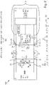
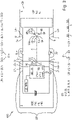
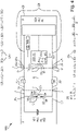
- Figures 1 to 4 and 5 show, in particular each, a system 100 according to the invention and a method according to the invention for determining at least one power contact resistance LR+, LR- between at least one pack power contact 2+, 2- of a battery pack 1 and at least one device power contact 5+, 5- of an electrically driven processing device 3 or one Charger 4 or at least one of the at least one power contact resistance corresponding resistance value.
- the at least one pack power contact 2+, 2- and the at least one device power contact 5+, 5- touch one another and are loaded with a power current LI.
- the battery pack 1 and the processing device 3 or the charging device 4 are electrically connected, in particular transmitted, by means of, in particular only, one, in particular a single, data communication line 6 for transmitting a data communication signal DS.
- the system 100 in particular a battery management system 101 of the system 100, is for determining the at least one power contact resistance LR+, LR- or the at least one resistance value by comparing a signal voltage magnitude SG+, SG- of the data communication line 6 and a power voltage magnitude LG+, LG- of the at least one pack power contact 2+, 2- or the at least one device power contact 5+, 5- is formed with one another, in particular compared and determined.
- the method includes: determining the at least one power contact resistance LR+, LR- or the at least one resistance value by comparing the signal voltage magnitude SG+, SG- of the data communication line 6 and the power voltage magnitude LG+, LG- of the at least one pack power contact 2+, 2- or the at least one Device power contact 5+, 5- with each other, in particular by means of the system 100, in particular the battery management system 101.
- the signal voltage magnitude SG+, SG- or the power voltage magnitude LG+, LG- depends on at least one voltage drop ⁇ U+, ⁇ U- caused by the power current LI and the at least one power contact resistance LR+, LR-.
- the method includes: determining the at least one power contact resistance LR+, LR- or the at least one resistance value by determining the power current LI, in particular by means of the system 100, in particular the battery management system 101.
- the method includes: determining the signal voltage variable SG+, SG- and/or the power voltage variable LG+, LG-, in particular by means of the system 100, in particular the battery management system 101.
- system 100 has the battery pack 1 , the processing device 3 and/or the charger 4 .
- the battery pack 1 has the battery management system 101 .
- a minus power contact resistance LR- between a minus pack power contact 2- of the battery pack 1 and a minus device power contact 5- of the processing device 3 is determined by comparing a minus signal voltage magnitude SG- of the data communication line 6 and a minus power voltage magnitude LG- of the minus pack power contact 2- determined, in particular by means of the system 100, in particular the battery management system 101.
- the minus pack power contact 2- and the minus device power contact 5- touch one another and are loaded with the power current LI.
- the minus signal voltage magnitude SG- depends on a minus voltage drop ⁇ U- caused by the power current LI and the minus power contact resistance LR-.
- a plus power contact resistance LR+ between a plus pack power contact 2+ of the battery pack 1 and a plus device power contact 5+ of the processing device 3 is determined by comparing a plus signal voltage magnitude SG+ of the data communication line 6 and a plus power voltage magnitude LG+ of the plus pack power contact 2+ , in particular by means of the system 100, in particular the battery management system 101.
- the plus pack power contact 2+ and the plus device power contact 5+ touch one another and are loaded with the power current LI.
- the plus signal voltage magnitude SG+ depends on the minus voltage drop ⁇ U- caused by the power current LI and the minus power contact resistance LR- and a plus voltage drop ⁇ U+ caused by the power current LI and the plus power contact resistance LR+.
- the processing device 3 has the battery management system 101 .
- the negative power contact resistance LR- between the negative pack power contact 2- of the battery pack 1 and the negative device power contact 5- of the processing device 3 is determined by comparing a negative signal voltage magnitude SG- of the data communication line 6 and a negative power voltage magnitude LG- of the negative Device power contact 5- determined, in particular by means of the system 100, in particular the battery management system 101.
- the negative pack power contact 2 and the negative device power contact 5- touch each other and are loaded with the power current LI.
- the minus power voltage magnitude LG- depends on the minus voltage drop ⁇ U- caused by the power current LI and the minus power contact resistance LR-.
- the plus power contact resistance LR+ between the plus pack power contact 2+ of the battery pack 1 and the plus device power contact 5+ of the processing device 3 is determined by comparing a plus signal voltage magnitude SG+ of the data communication line 6 and a plus power voltage magnitude LG+ of the plus device power contact 5+ , in particular by means of the system 100, in particular the battery management system 101.
- the plus pack power contact 2+ and the plus device power contact 5+ touch one another and are loaded with the power current LI.
- the plus power voltage size LG+ depends on the minus voltage drop ⁇ U- caused by the power current LI and the minus power contact resistance LR- and the plus voltage drop ⁇ U+ caused by the power current LI and the plus power contact resistance LR+.
- the battery pack 1 has the battery management system 101 .
- a minus power contact resistance LR- between the minus pack power contact 2- of the battery pack 1 and a minus device power contact 5- of the charger 4 is determined by comparing a minus signal voltage magnitude SG- of the data communication line 6 and a minus power voltage magnitude LG- of the minus pack power contact 2- determined, in particular by means of the system 100, in particular the battery management system 101.
- the minus pack power contact 2- and the minus device power contact 5- touch one another and are loaded with the power current LI.
- the minus power voltage magnitude LG- depends on a minus voltage drop ⁇ U- caused by the power current LI and the minus power contact resistance LR-.
- a plus power contact resistance LR+ between the plus pack power contact 2+ of the battery pack 1 and a plus device power contact 5+ of the charger 4 is determined by comparing a plus signal voltage magnitude SG+ of the data communication line 6 and a plus power voltage magnitude LG+ of the plus pack power contact 2+ , in particular by means of the system 100, in particular the battery management system 101.
- the plus pack power contact 2+ and the plus device power contact 5+ touch one another and are loaded with the power current LI.
- the plus power voltage magnitude LG+ depends on the minus voltage drop ⁇ U- caused by the power current LI and the minus power contact resistance LR- and a plus voltage drop ⁇ U+ caused by the power current LI and the plus power contact resistance LR+.
- the charger 4 has the battery management system 101 .
- the minus power contact resistance LR- between the minus pack power contact 2- of the battery pack 1 and the minus device power contact 5- of the charger 4 is determined by comparing a minus signal voltage magnitude SG- of the data communication line 6 and a minus power voltage magnitude LG- of the minus Device power contact 5- determined, in particular by means of the system 100, in particular the battery management system 101.
- the negative pack power contact 2 and the negative device power contact 5- touch each other and are loaded with the power current LI.
- the minus signal voltage magnitude SG- depends on the minus voltage drop ⁇ U- caused by the power current LI and the minus power contact resistance LR-.
- the plus power contact resistance LR+ between the plus pack power contact 2+ of the battery pack 1 and the plus device power contact 5+ of the charger 4 is determined by comparing a plus signal voltage magnitude SG+ of the data communication line 6 and a plus power voltage magnitude LG+ of the plus device power contact 5+ , in particular by means of the system 100, in particular the battery management system 101.
- the plus pack power contact 2+ and the plus device power contact 5+ touch one another and are loaded with the power current LI.
- the plus signal voltage magnitude SG+ depends on the minus voltage drop ⁇ U- caused by the power current LI and the minus power contact resistance LR- and the plus voltage drop ⁇ U+ caused by the power current LI and the plus power contact resistance LR+.
- a sum of, in particular, the negative power contact resistance and, in particular, the positive power contact resistance can be determined. Additionally or alternatively, in alternative embodiments, one, in particular, the minus signal voltage magnitude and/or one, in particular, the plus signal voltage magnitude and/or one, in particular, the minus power voltage magnitude and/or one, in particular, the plus power voltage magnitude depend on one, in particular the negative voltage drop caused by the power current and the negative power contact resistance and/or one, in particular the positive voltage drop caused by the power current and the positive power contact resistance.
- the data communication line 6 is different from the at least one pack power contact 2+, 2- and the at least one device power contact 5+, 5-.
- the battery pack 1 has, in particular, only one, in particular a single, pack data contact 7 that is different from the at least one pack power contact 2+, 2-.
- the processing device 3 or the charging device 4 has, in particular, only one device data contact 8, in particular a single device data contact 8, which is different from the at least one device power contact 5+, 5-.
- the pack data contact 7 and the device data contact 8 touch each other.
- the data communication line 6 is at least partially established by touching the pack data contact 7 and the device data contact 8 .
- the method includes: comparing by determining a deviation DI-, DI+, in particular a difference DI - , DI + , the signal voltage magnitude SG+, SG- and the Power voltage size LG+, LG- from each other, in particular by means of the system 100, in particular the battery management system 101.
- the minus power voltage magnitude LG- is a minus power voltage potential LP- of the minus pack power contact 2-.
- the plus power voltage magnitude LG+ is a plus power voltage potential LP+ of the plus pack power contact 2+ and/or a power voltage difference LDI between the plus power voltage potential LP+ of the plus pack power contact 2+ and the minus power voltage potential LP- of the minus pack power contact 2-.
- the minus power voltage magnitude LG- is a minus power voltage potential LP- of the minus device power contact 5-.
- the plus power voltage magnitude LG+ is a plus power voltage potential LP+ of the plus device power contact 5+ and/or a power voltage difference LDI between the plus power voltage potential LP+ of the plus device power contact 5+ and the minus power voltage potential LP- of the minus device power contact 5-.
- the minus signal voltage level SG- is a low signal voltage level low on the data communication line 6.
- the plus signal voltage level SG+ is a high signal voltage level high on the data communication line 6 and/or a signal voltage difference SDI between the high signal voltage level high and the low signal voltage level low .
- In 1 and 2 has the method: determining the negative power contact resistance LR- between the negative pack power contact 2- of the battery pack 1 and the negative device power contact 5- of the processing device 3 by comparing the negative signal voltage level low and the negative power voltage potential LP- with one another.
- the negative signal voltage level low depends on the negative voltage drop ⁇ U caused by the power current LI and the negative power contact resistance LR-.
- the negative power voltage potential LP- depends on the negative voltage drop ⁇ U caused by the power current LI and the negative power contact resistance LR-.
- the method also includes: determining the plus power contact resistance LR+ between the plus pack power contact 2+ of the battery pack 1 and the plus device power contact 5+ of the processing device 3 by comparing the signal voltage difference SDI and the power voltage difference LDI with one another.
- the signal voltage difference SDI depends on the minus voltage drop ⁇ U- caused by the power current LI and the minus power contact resistance LR- and the plus voltage drop ⁇ U+ caused by the power current LI and the plus power contact resistance LR+.
- the power voltage difference LDI depends on the minus voltage drop ⁇ U- caused by the power current LI and the minus power contact resistance LR- and the plus voltage drop ⁇ U+ caused by the power current LI and the plus power contact resistance LR+.
- In 3 and 4 has the method: determining the minus power contact resistance LR- between the minus pack power contact 2- of the battery pack 1 and the minus device power contact 5- of the charger 4 by comparing the minus signal voltage level low and the minus power voltage potential LP- with one another.
- the negative power voltage potential LP- depends on the negative voltage drop ⁇ U caused by the power current LI and the negative power contact resistance LR-.
- the negative signal voltage level low depends on the negative voltage drop ⁇ U caused by the power current LI and the negative power contact resistance LR-.
- the method also includes: determining the plus power contact resistance LR+ between the plus pack power contact 2+ of the battery pack 1 and the plus device power contact 5+ of the charger 4 by comparing the signal voltage difference SDI and the power voltage difference LDI with one another.
- the power voltage difference LDI depends on the minus voltage drop ⁇ U- caused by the power current LI and the minus power contact resistance LR- and the plus voltage drop ⁇ U+ caused by the power current LI and the plus power contact resistance LR+.
- the signal voltage difference SDI depends on the minus voltage drop ⁇ U- caused by the power current LI and the minus power contact resistance LR- and the plus voltage drop ⁇ U+ caused by the power current LI and the plus power contact resistance LR+.
- the minus signal voltage magnitude SG- is referenced to the minus power voltage potential LP- of the minus device power contact 5-.
- the plus signal voltage magnitude SG+ is referenced to the minus power voltage potential LP- of the minus device power contact 5- and/or depends on the power voltage difference LDI between the plus power voltage potential LP+ of the plus device power contact 5+ and the minus power voltage potential LP- of the minus- device power contact 5- off.
- the minus signal voltage magnitude SG- is referenced to the minus power voltage potential LP- of the minus pack power contact 2-.
- the plus signal voltage magnitude SG+ is referenced to the minus power voltage potential LP- of the minus pack power contact 2- and/or depends on the power voltage difference LDI between the plus power voltage potential LP+ of the plus pack power contact 2+ and the minus power voltage potential LP- of the minus- Packing service contact 2- from.
- the signal voltage magnitude may be referenced to the plus power voltage potential of the plus device power pin or the plus pack power pin.
- the data communication line 6 is connected to a signal output 9A of a transmitter 9, in particular an amplifier circuit 10 1 of processing device 3, in 3 of the charger 4 and in 2 and 4 of the battery pack 2, electrically connected.
- a minus supply voltage potential 9P- of the transmitter 9 depends on the minus voltage drop ⁇ U- caused by the power current LI and the minus power contact resistance LR-.
- a plus supply voltage potential 9P+ of the transmitter 9 depends on the minus voltage drop ⁇ U- caused by the power current LI and the minus power contact resistance LR- and the plus voltage drop ⁇ U+ caused by the power current LI and the plus power contact resistance LR+.
- the transmitter 9 has a supply voltage feedthrough.
- the minus supply voltage potential 9P- of the transmitter 9 is referenced to the minus power voltage potential LP- of the minus device power contact 5-, in particular the minus power voltage potential is LP-.
- the plus supply voltage potential 9P+ of the transmitter 9 is referenced to the plus power voltage potential LP+ of the plus device power contact 5+, in particular the plus power voltage potential is LP+.
- the minus supply voltage potential 9P- of the transmitter 9 is referenced to the minus power voltage potential LP- of the minus pack power contact 2-, in particular the minus power voltage potential is LP-.
- the plus supply voltage potential 9P+ of the transmitter 9 is at the plus power voltage potential LP+ of the plus pack power contact 2+ references, in particular the plus power voltage potential is LP+.
- a negative supply voltage input 9E- of the transmitter 9 is electrically connected to the negative device power contact 5-, in particular connected in parallel.
- a plus supply voltage input 9E+ of the transmitter 9 is electrically connected to the plus device power contact 5+, in particular connected in parallel.
- the negative supply voltage input 9E- of the transmitter 9 is electrically connected to the negative packing power contact 2-, in particular connected in parallel.
- the plus supply voltage input 9E+ of the transmitter 9 is electrically connected to the plus pack power contact 2+, in particular connected in parallel.
- the data communication line 6 is connected to a signal input 11E of a receiver 11, in 1 and 3 of the battery pack 2, in 2 of the processing device 3 and in 4 of the charger 4, in particular the battery management system 101, electrically connected.
- the data communication signal DS also has operating data information BI, speed information nl, current information SI, voltage information UI, power information LI, discharge information EI, charging information AI, temperature Information TI, status information ZI, error information FI and/or identifier information II.
- the at least one pack power contact 2+, 2- and/or the at least one device power contact 5+, 5- is/is a plug connector 12.
- a nominal voltage NSP of the battery pack 1, the processing device 3 and/or the charger 4 is at least 18 V, in particular a minimum of 30 V, and/or a maximum of 72 V, in particular a maximum of 54 V.
- a maximum power current mLI of the battery pack 1, the processing device 3 and/or the charger 4 is at least 1 A, in particular a minimum of 1.5 A, and/or a maximum of 1000 A, in particular a maximum of 750 A.
- a maximum power mL of the battery pack 1, the processing device 3 and/or the charger 4 is at least 1 kW, in particular a minimum of 2 kW, and/or a maximum of 10 kW, in particular a maximum of 5 kW.
- a maximum energy content mEI of the battery pack 1 is at least 100 Wh, in particular at least 200 Wh, and/or at most 4000 Wh, in particular at most 2000 Wh.
- system 100 in 1 and 3 the battery pack 1, in 2 the processing device 3 and in 4 the charger 4, an, in particular electrical, output and / or transmission device 13 on.
- the output and/or transmission device can have a display, a sound generator and/or a vibration device. Additionally or alternatively, the output and/or transmission device can have a transmission device, in particular an electrical and/or wireless transmission device. In particular, the transmission device can have, in particular be, a UMTS, WLAN and/or Bluetooth transmission device or a transmission device based on another technology.
- the method also includes: outputting and/or transmitting information about the at least one specific power contact resistance LR+, LR- or the at least one specific resistance value, in particular if the at least one specific power contact resistance LR+, LR- or the at least one specific resistance value has a resistance limit value RG reached or exceeded, in particular by means of the output and/or transmission device 13.
- the at least one specific power contact resistance LR+, LR- or the at least one specific resistance value reaches or exceeds the resistance limit value RG, reducing a maximum released power mfL and/or a maximum released power current mfLI, in particular switching off the battery pack 1 of the processing device 3 and/or the charger 4, in particular by means of the battery management system 101.
- the battery management system 101 and the output and/or transmission device 13 are signal-connected.
- figure 5 the processing device 3 is a saw 3', in particular a chain saw 3".
- the processing device can be a pole pruner, a brush cutter, a hedge trimmer, a hedge trimmer, a blower, a leaf blower, a pruning shears, a cut-off grinder, a sweeper, a roller brush, a sweeping brush, a lawnmower, a scarifier, grass shears or be a pressure washer.
- the processing device 3 and/or the charging device 4 has a battery holder 14, in particular a battery compartment 14'.
- the battery holder 14 is designed to hold the battery pack 1, in particular the battery pack 1 is held.
- the invention provides an advantageous method and an advantageous system for determining at least one power contact resistance between at least one pack power contact of a battery pack and at least one device power contact of an electrically driven processing device or a charger or at least one of the at least one power contact resistance corresponding resistance value ready, each having improved properties.
Landscapes
- Physics & Mathematics (AREA)
- General Physics & Mathematics (AREA)
- Engineering & Computer Science (AREA)
- Power Engineering (AREA)
- Microelectronics & Electronic Packaging (AREA)
- Manufacturing & Machinery (AREA)
- Chemical & Material Sciences (AREA)
- Chemical Kinetics & Catalysis (AREA)
- Electrochemistry (AREA)
- General Chemical & Material Sciences (AREA)
- Charge And Discharge Circuits For Batteries Or The Like (AREA)
Abstract
Description
- Die Erfindung bezieht sich auf ein Verfahren und ein System zum Bestimmen mindestens eines Leistungskontaktwiderstands zwischen mindestens einem Packleistungskontakt eines Akkupacks und mindestens einem Geräteleistungskontakt eines elektrisch angetriebenen Bearbeitungsgeräts oder eines Ladegeräts oder mindestens eines dem mindestens einen Leistungskontaktwiderstand korrespondierenden Widerstandswerts.
- Der Erfindung liegt als Aufgabe die Bereitstellung eines Verfahrens und eines Systems jeweils zum Bestimmen mindestens eines Leistungskontaktwiderstands zwischen mindestens einem Packleistungskontakt eines Akkupacks und mindestens einem Geräteleistungskontakt eines elektrisch angetriebenen Bearbeitungsgeräts oder eines Ladegeräts oder mindestens eines dem mindestens einen Leistungskontaktwiderstand korrespondierenden Widerstandswerts zugrunde, das jeweils verbesserte Eigenschaften aufweist bzw. hat.
- Die Erfindung löst die Aufgabe durch die Bereitstellung eines Verfahrens mit den Merkmalen des Anspruchs 1 und eines Systems mit den Merkmalen des Anspruchs 14. Vorteilhafte Weiterbildungen und/oder Ausgestaltungen der Erfindung sind in den abhängigen Ansprüchen beschrieben.
- Das erfindungsgemäße, insbesondere automatische, Verfahren ist zum, insbesondere automatischen und/oder mittelbaren bzw. indirekten, Bestimmen, insbesondere Messen, mindestens eines, insbesondere elektrischen, Leistungskontaktwiderstands, insbesondere mindestens eines Werts mindestens des Leistungskontaktwiderstands, zwischen mindestens einem, insbesondere elektrischen, Packleistungskontakt eines Akkupacks (Englisch: battery pack) und mindestens einem, insbesondere elektrischen, Geräteleistungskontakt eines elektrisch angetriebenen Bearbeitungsgeräts oder eines, insbesondere elektrischen, Ladegeräts oder mindestens eines dem mindestens einen Leistungskontaktwiderstand korrespondierenden Widerstandswerts ausgebildet bzw. konfiguriert bzw. vorgesehen. Der mindestens eine Packleistungskontakt und der mindestens eine Geräteleistungskontakt berühren bzw. kontaktieren einander bzw. sich, insbesondere mechanisch und/oder elektrisch und/oder unmittelbar, und sind mit einem, insbesondere elektrischen, Leistungs- bzw. Betriebsstrom belastet. Der Akkupack und das Bearbeitungsgerät oder das Ladegerät sind mittels einer Datenkommunikationsleitung zum Übertragen bzw. Kommunizieren eines, insbesondere elektrischen, Datenkommunikationssignals elektrisch, insbesondere galvanisch, verbunden. Das Verfahren umfasst bzw. weist, insbesondere den Schritt, auf: Bestimmen, insbesondere automatisches und/oder mittelbares bzw. indirektes Bestimmen und/oder Messen, des mindestens einen Leistungskontaktwiderstands oder des mindestens einen Widerstandswerts mittels Vergleichens einer, insbesondere elektrischen, Signalspannungsgröße, insbesondere eines Werts der Signalspannungsgröße, der Datenkommunikationsleitung und einer, insbesondere elektrischen, Leistungsspannungsgröße, insbesondere eines Werts der Leistungsspannungsgröße, des mindestens einen Packleistungskontakts oder des mindestens einen Geräteleistungskontakts miteinander. Insbesondere entweder, die Signalspannungsgröße oder die Leistungsspannungsgröße, insbesondere selbst, hängt von mindestens einem, insbesondere elektrischen, Spannungsabfall, insbesondere mindestens einem Wert mindestens des Spannungsabfalls, verursacht durch den Leistungsstrom, insbesondere einen Wert des Leistungsstroms, und den mindestens einen Leistungskontaktwiderstand ab.
- Dies ermöglicht ein mittelbares und/oder, insbesondere somit, einfaches und/oder kostengünstiges Bestimmen des mindestens einen Leistungskontaktwiderstands oder des mindestens einen Widerstandswerts, insbesondere mit vorhandenen Mitteln.
- Insbesondere kann die Datenkommunikationsleitung und/oder, insbesondere somit, die Signalspannungsgröße, insbesondere bereits, vorhanden sein.
- Zusätzlich oder alternativ braucht oder kann der mindestens eine Leistungskontaktwiderstand und/oder der mindestens eine Widerstandswert nicht mittels einer, insbesondere getrennten bzw. separaten, Vierpunktmessung, insbesondere mittels zusätzlicher Messkontakte, bestimmt werden.
- Weiter zusätzlich oder alternativ braucht oder kann das Datenkommunikationssignal keine Information für und/oder über das Bestimmen des mindestens einen Leistungskontaktwiderstands oder des mindestens einen Widerstandswerts aufweisen. Weiter zusätzlich oder alternativ, insbesondere stattdessen, kann die Signalspannungsgröße von dem mindestens einen Spannungsabfall abhängen.
- Das Datenkommunikationssignal kann mittels der Signalspannungsgröße übertragen werden.
- Der Leistungsstrom kann mittels des mindestens einen Packleistungskontakts und des mindestens einen Geräteleistungskontakts übertragen werden.
- Der Leistungsstrom kann von Null verschieden und/oder zur Aufladung und/oder zur Entladung des Akkupacks, insbesondere zum Antrieb des Bearbeitungsgeräts, insbesondere eines Antriebsmotors des Bearbeitungsgeräts, sein.
- Das Verfahren, insbesondere das Vergleichen, kann aufweisen: Bestimmen, insbesondere Messen, der Signalspannungsgröße und/oder der Leistungsspannungsgröße.
- Die Signalspannungsgröße und die Leistungsspannungsgröße können verschieden sein.
- Der/die Kontakt/e kann/können als Klemme/n bzw. Anschluss/Anschlüsse bzw. Terminal/s bezeichnet werden.
- Die Berührung des mindestens einen Packleistungskontakts und des mindestens einen Geräteleistungskontakts kann, insbesondere werkzeugfrei und/oder zerstörungsfrei, lösbar sein. In anderen Worten: Der Akkupack kann zur, insbesondere werkzeugfrei und/oder zerstörungsfrei, lösbaren, insbesondere elektrischen und/oder mechanischen, Verbindung mit dem Bearbeitungsgerät und/oder dem Ladegerät ausgebildet sein. Insbesondere kann der Akkupack zum Tragen durch das Bearbeitungsgerät und/oder das Ladegerät ausgebildet sein. Insbesondere kann das Bearbeitungsgerät und/oder das Ladegerät, insbesondere jeweils, eine Akkuaufnahme, insbesondere einen Akkuschacht, aufweisen, wobei die Akkuaufnahme zum Aufnehmen des Akkupacks ausgebildet sein kann.
- Das Bearbeitungsgerät kann ein Garten-, Forst-, Bau- und/oder Bodenbearbeitungsgerät, insbesondere eine Säge, insbesondere eine Kettensäge, ein Hoch-Entaster, ein Freischneider, eine Heckenschere, ein Heckenschneider, ein Blasgerät, ein Laubbläser, eine Astschere, ein Trennschleifer, ein Kehrgerät, eine Kehrwalze, eine Kehrbürste, ein Rasenmäher, ein Vertikutierer, eine Grasschere oder ein Hochdruckreiniger, sein. Zusätzlich oder alternativ kann das Bearbeitungsgerät boden- und/oder handgeführt, insbesondere handgetragen, sein. Insbesondere handgeführtes, insbesondere handgetragenes, Bearbeitungsgerät kann bedeuten, dass das Bearbeitungsgerät eine Masse von maximal 50 kg (Kilogramm), insbesondere maximal 20 kg, insbesondere maximal 10 kg, aufweisen bzw. haben kann.
- Der Akkupack kann eine Mehrzahl von Akkumulatorzellen aufweisen. Insbesondere können die Akkumulatorzellen jeweils einzelne wiederaufladbare Speicherelemente für elektrische Energie auf elektrochemischer Basis sein. Zusätzlich oder alternativ können die Akkumulatorzellen Lithium-Ionen-Akkumulatorzellen sein. Weiter zusätzlich oder alternativ können die Akkumulatorzellen gleich, insbesondere typ- und/oder baugleich, sein. Weiter zusätzlich oder alternativ kann eine, insbesondere jeweilige, Zell-Spannung, insbesondere Zell-Nennspannung, einer, insbesondere jeweiligen, der Akkumulatorzellen minimal 2 V (Volt) und/oder maximal 4 V, insbesondere 3,6 V, sein. Weiter zusätzlich oder alternativ können die Akkumulatorzellen Rundzellen, prismatische Zellen oder Pouchzellen sein.
- In einer Weiterbildung der Erfindung weist das Verfahren, insbesondere das Vergleichen, auf: Bestimmen des mindestens eines Leistungskontaktwiderstands oder des mindestens einen Widerstandswerts mittels Bestimmens, insbesondere automatischen und/oder unmittelbaren bzw. direkten Bestimmens und/oder Messens, des Leistungsstroms.
- In einer Weiterbildung der Erfindung ist die Datenkommunikationsleitung von dem mindestens einen Packleistungskontakt und dem mindestens einen Geräteleistungskontakt verschieden bzw. getrennt, insbesondere elektrisch isoliert. Insbesondere umfasst bzw. weist der Akkupack einen von dem mindestens einen Packleistungskontakt verschiedenen bzw. getrennten, insbesondere elektrisch isolierten, insbesondere elektrischen, Packdatenkontakt auf. Das Bearbeitungsgerät oder das Ladegerät umfasst bzw. weist einen von dem mindestens einen Geräteleistungskontakt verschiedenen bzw. getrennten, insbesondere elektrisch isolierten, insbesondere elektrischen, Gerätedatenkontakt auf. Der Packdatenkontakt und der Gerätedatenkontakt berühren bzw. kontaktieren einander bzw. sich, insbesondere mechanisch und/oder elektrisch und/oder unmittelbar. Die Datenkommunikationsleitung ist mindestens teilweise, insbesondere vollständig, durch die Berührung des Packdatenkontakts und des Gerätedatenkontakts hergestellt bzw. gebildet. Dies ermöglicht, dass, insbesondere entweder, die Signalspannungsgröße oder die Leistungsspannungsgröße von dem mindestens einen Spannungsabfall abhängen kann. Insbesondere kann ein Strom und somit ein Spannungsabfall über die Datenkommunikationsleitung verursacht durch den Strom und einen Kontaktwiderstand zwischen dem Packdatenkontakt und dem Gerätedatenkontakt gegenüber dem Leistungsstrom und dem mindestens einen Leistungskontaktwiderstand vernachlässigbar, insbesondere niedrig, sein.
- In einer Weiterbildung der Erfindung weist das Verfahren auf: Vergleichen mittels Ermittelns, insbesondere automatischen Ermittelns und/oder Bestimmens und/oder Messens und/oder Berechnens, einer Abweichung, insbesondere eines Werts der Abweichung und/oder einer Differenz, der Signalspannungsgröße und der Leistungsspannungsgröße voneinander.
- In einer Weiterbildung der Erfindung ist die Leistungsspannungsgröße ein Leistungsspannungspotential, insbesondere ein Minus-Leistungsspannungspotential und/oder ein Plus-Leistungsspannungspotential, des Packleistungskontakts, insbesondere eines Minus-Packleistungskontakts und/oder eines Plus-Packleistungskontakts, und/oder eine Leistungsspannungsdifferenz zwischen dem Plus-Leistungsspannungspotential des Plus-Packleistungskontakts und dem Minus-Leistungsspannungspotential des Minus-Packleistungskontakts. Alternativ ist die Leistungsspannungsgröße ein Leistungsspannungspotential, insbesondere ein Minus-Leistungsspannungspotential und/oder ein Plus-Leistungsspannungspotential, des Geräteleistungskontakts, insbesondere eines Minus-Geräteleistungskontakts und/oder eines Plus-Geräteleistungskontakts, und/oder eine Leistungsspannungsdifferenz zwischen dem Plus-Leistungsspannungspotential des Plus-Geräteleistungskontakts und dem Minus-Leistungsspannungspotential des Minus-Geräteleistungskontakts. Eine derartige Leistungsspannungsgröße ist für das Vergleichen besonders geeignet, insbesondere vorteilhaft.
- In einer Weiterbildung der Erfindung ist die Signalspannungsgröße ein Signalspannungspegel bzw. -potential, insbesondere ein niedriger Signalspannungspegel oder ein hoher Signalspannungspegel, der Datenkommunikationsleitung und/oder eine Signalspannungsdifferenz bzw. -amplitude bzw. ein Signalspannungshub zwischen dem hohen Signalspannungspegel und dem niedrigen Signalspannungspegel. Eine derartige Signalspannungsgröße ist für das Vergleichen besonders geeignet, insbesondere vorteilhaft. Insbesondere kann das Datenkommunikationssignal binär sein. Im Übrigen wird auf die Fachliteratur verwiesen.
- In einer Ausgestaltung der Erfindung weist das Verfahren auf: Bestimmen eines, insbesondere ersten, Leistungskontaktwiderstands zwischen einem, insbesondere ersten, Packleistungskontakt des Akkupacks und einem, insbesondere ersten, Geräteleistungskontakt des Bearbeitungsgeräts oder des Ladegeräts oder eines dem Leistungskontaktwiderstand korrespondierenden, insbesondere ersten, Widerstandswerts mittels Vergleichens des Signalspannungspegels und des Leistungsspannungspotentials miteinander. Insbesondere entweder, der Signalspannungspegel oder das Leistungsspannungspotential hängt von einem, insbesondere ersten, Spannungsabfall verursacht durch den Leistungsstrom und den Leistungskontaktwiderstand ab. Zusätzlich oder alternativ, insbesondere zeitlich danach, Bestimmen eines, insbesondere zweiten und/oder anderen, Leistungskontaktwiderstands zwischen einem, insbesondere zweiten und/oder anderen, Packleistungskontakt des Akkupacks und einem, insbesondere zweiten und/oder anderen, Geräteleistungskontakt des Bearbeitungsgeräts oder des Ladegeräts oder eines dem Leistungskontaktwiderstand korrespondierenden, insbesondere zweiten und/oder anderen, Widerstandswerts mittels Vergleichens der Signalspannungsdifferenz und der Leistungsspannungsdifferenz miteinander. Insbesondere entweder, die Signalspannungsdifferenz oder die Leistungsspannungsdifferenz hängt von mindestens einem, insbesondere zweiten und/oder anderen, Spannungsabfall verursacht durch den Leistungsstrom und den mindestens einen Leistungskontaktwiderstand ab. Dies ermöglicht das Bestimmen eines Plus-Leistungskontaktwiderstands oder eines korrespondierenden Plus-Widerstandswerts und/oder eines Minus-Leistungskontaktwiderstands oder eines korrespondierenden Minus-Widerstandswerts, insbesondere jeweils, bzw. dieser verschiedenen Leistungskontaktwiderstände oder Widerstandswerte.
- In einer Weiterbildung der Erfindung ist, insbesondere entweder, die Signalspannungsgröße auf ein Leistungsspannungspotential, insbesondere ein Minus-Leistungsspannungspotential und/oder ein Plus-Leistungsspannungspotential, des Geräteleistungskontakts, insbesondere eines Minus-Geräteleistungskontakts und/oder eines Plus-Geräteleistungskontakts, referenziert und/oder hängt von einer Leistungsspannungsdifferenz zwischen dem Plus-Leistungsspannungspotential des Plus-Geräteleistungskontakts und dem Minus-Leistungsspannungspotential des Minus-Geräteleistungskontakts ab. Alternativ bzw. oder ist die Signalspannungsgröße auf ein Leistungsspannungspotential, insbesondere ein Minus-Leistungsspannungspotential und/oder ein Plus-Leistungsspannungspotential, des Packleistungskontakts, insbesondere eines Minus-Packleistungskontakts und/oder eines Plus-Packleistungskontakts, referenziert und/oder hängt von einer Leistungsspannungsdifferenz zwischen dem Plus-Leistungsspannungspotential des Plus-Packleistungskontakts und dem Minus-Leistungsspannungspotential des Minus-Packleistungskontakts ab. Dies ermöglicht, dass, insbesondere entweder, die Signalspannungsgröße oder die Leistungsspannungsgröße von dem mindestens einen Spannungsabfall abhängen kann.
- In einer Weiterbildung der Erfindung ist die Datenkommunikationsleitung mit einem Signalausgang eines, insbesondere elektrischen, Senders, insbesondere einer Verstärkerschaltung, insbesondere des Bearbeitungsgeräts oder des Ladegeräts oder des Akkupacks, elektrisch, insbesondere galvanisch, verbunden. Mindestens ein, insbesondere elektrisches, Versorgungsspannungspotential des Senders hängt von mindestens einem, insbesondere dem mindestens einen, Spannungsabfall verursacht durch den Leistungsstrom und den mindestens einen Leistungskontaktwiderstand ab. Insbesondere hat bzw. weist der Sender einen Versorgungsspannungsdurchgriff auf. Zusätzlich oder alternativ ist mindestens ein, insbesondere elektrisches, Versorgungsspannungspotential des Senders auf mindestens ein Leistungsspannungspotential des mindestens einen Geräteleistungskontakts oder mindestens ein Leistungsspannungspotential des mindestens einen Packleistungskontakts referenziert, insbesondere ist das mindestens eine Leistungsspannungspotential. Weiter zusätzlich oder alternativ ist mindestens ein Versorgungsspannungseingang des Senders mit dem mindestens einen Geräteleistungskontakt oder dem mindestens einen Packleistungskontakt elektrisch, insbesondere galvanisch, verbunden, insbesondere parallelgeschaltet. Dies ermöglicht, dass die Signalspannungsgröße von dem mindestens einen Spannungsabfall abhängen kann oder derartig wie vorhergehend genannt sein kann. Insbesondere kann die Datenkommunikationsleitung mit einem Signaleingang eines, insbesondere elektrischen, Empfängers, insbesondere des Akkupacks oder des Bearbeitungsgeräts oder des Ladegeräts, elektrisch, insbesondere galvanisch, verbunden sein. Zusätzlich oder alternativ kann das Datenkommunikationssignal mittels der Verstärkerschaltung verstärkt sein. Weiter zusätzlich oder alternativ kann die Verstärkerschaltung eine Operationsund/oder Differenzverstärkerschaltung aufweisen, insbesondere sein. Im Übrigen wird auf die Fachliteratur verwiesen.
- In einer Weiterbildung der Erfindung umfasst bzw. weist das Datenkommunikationssignal eine Betriebsdaten-Information, eine Drehzahl-Information, eine Strom-Information, eine Spannungs-Information, eine Leistungs-Information, eine Entladungs-Information, eine Aufladungs-Information, eine Temperatur-Information, eine Zustands-Information, eine Fehler-Information und/oder eine Identifikator-Information auf. Eine derartige Information/en ist/sind für einen Betrieb und/oder eine Auswertung des Betriebs des Akkupacks, des Bearbeitungsgeräts und/oder des Ladegeräts geeignet, insbesondere vorteilhaft. Insbesondere können/kann die Drehzahl-Information über eine Drehzahl und/oder die Strom-Information über einen Motorstrom eines Antriebsmotors des Bearbeitungsgeräts sein. Zusätzlich oder alternativ kann die Temperatur-Information über eine Temperatur eines Antriebsmotors des Bearbeitungsgeräts und/oder von Akkumulatorzellen des Akkupacks sein. Weiter zusätzlich oder alternativ können/kann die Zustands-Information über einen Zustand, die Fehler-Information über einen Fehler und/oder die Identifikator-Information über einen Identifikator des Bearbeitungsgeräts und/oder des Akkupacks sein. Weiter zusätzlich oder alternativ kann die, insbesondere jeweilige, Information von der Signalspannungsgröße verschieden, insbesondere verschiedenartig, sein. Im Übrigen wird auf die Fachliteratur verwiesen.
- In einer Weiterbildung der Erfindung sind/ist der mindestens eine Packleistungskontakt und/oder der mindestens eine Geräteleistungskontakt, insbesondere jeweils, ein Steckverbinder. Insbesondere kann der Steckverbinder ein Stecker oder eine, insbesondere korrespondierende, Buchse sein. Dies ermöglicht, dass der Leistungskontaktwiderstand nicht vernachlässigbar, insbesondere hoch, sein kann, und/oder die Lösbarkeit wie vorhergehend genannt.
- In einer Weiterbildung der Erfindung ist eine, insbesondere elektrische, Nennspannung des Akkupacks, des Bearbeitungsgeräts und/oder des Ladegeräts minimal 18 V, insbesondere minimal 30 V, und/oder maximal 72 V, insbesondere maximal 54 V. Zusätzlich oder alternativ ist ein maximaler, insbesondere elektrischer, Leistungsstrom, insbesondere Aufladungs- und/oder Entladungs-Leistungsstrom, insbesondere Antriebs-Leistungsstrom, des Akkupacks, des Bearbeitungsgeräts und/oder des Ladegeräts minimal 1 A (Ampere), insbesondere minimal 1,5 A, und/oder maximal 1000 A, insbesondere maximal 750 A. Weiter zusätzlich oder alternativ ist eine maximale, insbesondere elektrische, Leistung des Akkupacks, des Bearbeitungsgeräts und/oder des Ladegeräts minimal 1 kW (Kilowatt), insbesondere minimal 2 kW, und/oder maximal 10 kW, insbesondere maximal 5 kW. Weiter zusätzlich oder alternativ ist ein maximaler, insbesondere elektrischer, Energieinhalt, insbesondere Nennenergieinhalt, des Akkupacks minimal 100 Wh (Wattstunden), insbesondere minimal 200 Wh, und/oder maximal 4000 Wh, insbesondere maximal 2000 Wh. Dies ermöglicht, dass der Leistungskontaktwiderstand nicht vernachlässigbar, insbesondere hoch, sein kann.
- In einer Weiterbildung der Erfindung umfasst bzw. weist das Verfahren, insbesondere den Schritt, auf: Ausgeben, insbesondere automatisches Ausgeben, und/oder Übertragen, insbesondere automatisches Übertragen, einer, insbesondere benutzerwahrnehmbaren, Information über den mindestens einen bestimmten Leistungskontaktwiderstand oder den mindestens einen bestimmten Widerstandswert, insbesondere falls der mindestens eine bestimmte Leistungskontaktwiderstand oder der mindestens eine bestimmte Widerstandswert einen, insbesondere vorgegebenen, Widerstandsgrenzwert erreicht oder überschreitet. Zusätzlich oder alternativ, falls der mindestens eine bestimmte Leistungskontaktwiderstand oder der mindestens eine bestimmte Widerstandswert einen, insbesondere vorgegebenen, Widerstandsgrenzwert erreicht oder überschreitet, Absenken, insbesondere automatisches Absenken, einer maximal freigegebenen Leistung und/oder eines maximal freigegebenen Leistungsstroms, insbesondere Abschalten des Akkupacks, des Bearbeitungsgeräts und/oder des Ladegeräts. Dies ermöglicht einen Schutz, eine Reinigung, eine Wartung und/oder eine Reparatur des Akkupacks, des Bearbeitungsgeräts und/oder des Ladegeräts. Insbesondere kann die Information eine Schutz- Information, eine Reinigungs-Information, eine Wartungs-Information, eine Reparatur-Information und/oder eine Absenkungs-, insbesondere Abschaltungs-, Information aufweisen, insbesondere sein. Zusätzlich oder alternativ kann das Ausgeben optisch, akustisch und/oder haptisch sein. Weiter zusätzlich oder alternativ kann das Übertragen kabellos bzw. drahtlos sein und/oder ein Senden aufweisen, insbesondere sein.
- Das erfindungsgemäße, insbesondere elektrische, System ist zum Bestimmen mindestens eines, insbesondere des mindestens einen, Leistungskontaktwiderstands zwischen mindestens einem, insbesondere dem mindestens einen, Packleistungskontakt eines, insbesondere des, Akkupacks und mindestens einem, insbesondere dem mindestens einen, Geräteleistungskontakt eines, insbesondere des, elektrisch angetriebenen Bearbeitungsgeräts oder eines, insbesondere des, Ladegeräts oder mindestens eines, insbesondere dem mindestens einen, dem mindestens einen Leistungskontaktwiderstand korrespondierenden Widerstandswerts ausgebildet bzw. konfiguriert. Der mindestens eine Packleistungskontakt und der mindestens eine Geräteleistungskontakt berühren einander und sind mit einem, insbesondere dem, Leistungsstrom belastet. Der Akkupack und das Bearbeitungsgerät oder das Ladegerät sind mittels einer, insbesondere der, Datenkommunikationsleitung zum Übertragen eines, insbesondere des, Datenkommunikationssignals elektrisch verbunden. Das System ist zum Bestimmen des mindestens einen Leistungskontaktwiderstands oder des mindestens einen Widerstandswerts mittels Vergleichens einer, insbesondere der, Signalspannungsgröße der Datenkommunikationsleitung und einer, insbesondere der, Leistungsspannungsgröße des mindestens einen Packleistungskontakts oder des mindestens einen Geräteleistungskontakts miteinander ausgebildet bzw. konfiguriert. Die Signalspannungsgröße oder die Leistungsspannungsgröße hängt von mindestens einem, insbesondere dem mindestens einen, Spannungsabfall verursacht durch den Leistungsstrom und den mindestens einen Leistungskontaktwiderstand ab.
- Das System kann den/die gleichen Vorteil/e ermöglichen wie für das Verfahren vorhergehend genannt.
- Insbesondere kann das System, insbesondere ein Batteriemanagementsystem des Systems, zum, insbesondere automatischen, Ausführen eines, insbesondere des, Verfahrens wie vorhergehend genannt ausgebildet bzw. konfiguriert sein.
- In einer Weiterbildung der Erfindung umfasst bzw. weist das System den Akkupack, das Bearbeitungsgerät und/oder das Ladegerät auf. Insbesondere kann der Akkupack, das Bearbeitungsgerät und/oder das Ladegerät, insbesondere jeweils, ein, insbesondere das, Batteriemanagementsystem aufweisen bzw. umfassen.
- Weitere Vorteile und Aspekte der Erfindung ergeben sich aus den Ansprüchen und aus der Beschreibung von Ausführungsbeispielen der Erfindung, die nachfolgenden anhand der Figuren erläutert sind. Dabei zeigen:
- Fig. 1 bis 4
- schematische Ansichten, insbesondere Schaltpläne, insbesondere jeweils, eines erfindungsgemäßen Systems und eines erfindungsgemäßen Verfahrens, und
- Fig. 5
- eine Perspektivansicht des Systems der
Fig. 1 und2 . -
Fig. 1 bis 4 und5 zeigen, insbesondere jeweils, ein erfindungsgemäßes System 100 und ein erfindungsgemäßes Verfahren zum Bestimmen mindestens eines Leistungskontaktwiderstands LR+, LR- zwischen mindestens einem Packleistungskontakt 2+, 2- eines Akkupacks 1 und mindestens einem Geräteleistungskontakt 5+, 5- eines elektrisch angetriebenen Bearbeitungsgeräts 3 oder eines Ladegeräts 4 oder mindestens eines dem mindestens einen Leistungskontaktwiderstand korrespondierenden Widerstandswerts. Der mindestens eine Packleistungskontakt 2+, 2- und der mindestens eine Geräteleistungskontakt 5+, 5- berühren einander und sind mit einem Leistungsstrom LI belastet. Der Akkupack 1 und das Bearbeitungsgerät 3 oder das Ladegerät 4 sind mittels, insbesondere nur, einer, insbesondere einzigen, Datenkommunikationsleitung 6 zum Übertragen eines Datenkommunikationssignals DS elektrisch verbunden, insbesondere übertragen. - Das System 100, insbesondere ein Batteriemanagementsystem 101 des Systems 100, ist zum Bestimmen des mindestens einen Leistungskontaktwiderstands LR+, LR- oder des mindestens einen Widerstandswerts mittels Vergleichens einer Signalspannungsgröße SG+, SG- der Datenkommunikationsleitung 6 und einer Leistungsspannungsgröße LG+, LG- des mindestens einen Packleistungskontakts 2+, 2- oder des mindestens einen Geräteleistungskontakts 5+, 5-miteinander ausgebildet, insbesondere vergleicht und bestimmt.
- Das Verfahren weist auf: Bestimmen des mindestens einen Leistungskontaktwiderstands LR+, LR- oder des mindestens einen Widerstandswerts mittels Vergleichens der Signalspannungsgröße SG+, SG- der Datenkommunikationsleitung 6 und der Leistungsspannungsgröße LG+, LG- des mindestens einen Packleistungskontakts 2+, 2- oder des mindestens einen Geräteleistungskontakts 5+, 5- miteinander, insbesondere mittels des Systems 100, insbesondere des Batteriemanagementsystems 101.
- Die Signalspannungsgröße SG+, SG- oder die Leistungsspannungsgröße LG+, LG- hängt von mindestens einem Spannungsabfall ΔU+, ΔU- verursacht durch den Leistungsstrom LI und den mindestens einen Leistungskontaktwiderstand LR+, LR- ab.
- Im Detail weist das Verfahren auf: Bestimmen des mindestens eines Leistungskontaktwiderstands LR+, LR- oder des mindestens einen Widerstandswerts mittels Bestimmens des Leistungsstroms LI, insbesondere mittels des Systems 100, insbesondere des Batteriemanagementsystems 101.
- Des Weiteren weist in den gezeigten Ausführungsbeispielen das Verfahren auf: Bestimmen der Signalspannungsgröße SG+, SG- und/oder der Leistungsspannungsgröße LG+, LG-, insbesondere mittels des Systems 100, insbesondere des Batteriemanagementsystems 101.
- Außerdem weist das System 100 den Akkupack 1, das Bearbeitungsgerät 3 und/oder das Ladegerät 4 auf.
- In
Fig. 1 weist der Akkupack 1 das Batteriemanagementsystem 101 auf. - Weiter wird ein Minus-Leistungskontaktwiderstand LR- zwischen einem Minus-Packleistungskontakt 2- des Akkupacks 1 und einem Minus-Geräteleistungskontakt 5- des Bearbeitungsgeräts 3 mittels Vergleichens einer Minus-Signalspannungsgröße SG- der Datenkommunikationsleitung 6 und einer Minus-Leistungsspannungsgröße LG- des Minus-Packleistungskontakts 2- bestimmt, insbesondere mittels des Systems 100, insbesondere des Batteriemanagementsystems 101. Der Minus-Packleistungskontakt 2- und der Minus-Geräteleistungskontakt 5- berühren einander und sind mit dem Leistungsstrom LI belastet. Die Minus-Signalspannungsgröße SG- hängt von einem Minus-Spannungsabfall ΔU- verursacht durch den Leistungsstrom LI und den Minus-Leistungskontaktwiderstand LR- ab.
- Zudem wird ein Plus-Leistungskontaktwiderstand LR+ zwischen einem Plus-Packleistungskontakt 2+ des Akkupacks 1 und einem Plus-Geräteleistungskontakt 5+ des Bearbeitungsgeräts 3 mittels Vergleichens einer Plus-Signalspannungsgröße SG+ der Datenkommunikationsleitung 6 und einer Plus-Leistungsspannungsgröße LG+ des Plus-Packleistungskontakts 2+ bestimmt, insbesondere mittels des Systems 100, insbesondere des Batteriemanagementsystems 101. Der Plus-Packleistungskontakt 2+ und der Plus-Geräteleistungskontakt 5+ berühren einander und sind mit dem Leistungsstrom LI belastet. Die Plus-Signalspannungsgröße SG+ hängt von dem Minus-Spannungsabfall ΔU- verursacht durch den Leistungsstrom LI und den Minus-Leistungskontaktwiderstand LR- und einem Plus-Spannungsabfall ΔU+ verursacht durch den Leistungsstrom LI und den Plus-Leistungskontaktwiderstand LR+ ab.
- In
Fig. 2 weist das Bearbeitungsgerät 3 das Batteriemanagementsystem 101 auf. - Des Weiteren wird der Minus-Leistungskontaktwiderstand LR- zwischen dem Minus-Packleistungskontakt 2- des Akkupacks 1 und dem Minus-Geräteleistungskontakt 5- des Bearbeitungsgeräts 3 mittels Vergleichens einer Minus-Signalspannungsgröße SG- der Datenkommunikationsleitung 6 und einer Minus-Leistungsspannungsgröße LG- des Minus-Geräteleistungskontakts 5- bestimmt, insbesondere mittels des Systems 100, insbesondere des Batteriemanagementsystems 101. Der Minus-Packleistungskontakt 2- und der Minus-Geräteleistungskontakt 5- berühren einander und sind mit dem Leistungsstrom LI belastet. Die Minus-Leistungsspannungsgröße LG- hängt von dem Minus-Spannungsabfall ΔU- verursacht durch den Leistungsstrom LI und den Minus-Leistungskontaktwiderstand LR- ab.
- Außerdem wird der Plus-Leistungskontaktwiderstand LR+ zwischen dem Plus-Packleistungskontakt 2+ des Akkupacks 1 und dem Plus-Geräteleistungskontakt 5+ des Bearbeitungsgeräts 3 mittels Vergleichens einer Plus-Signalspannungsgröße SG+ der Datenkommunikationsleitung 6 und einer Plus-Leistungsspannungsgröße LG+ des Plus-Geräteleistungskontakts 5+ bestimmt, insbesondere mittels des Systems 100, insbesondere des Batteriemanagementsystems 101. Der Plus-Packleistungskontakt 2+ und der Plus-Geräteleistungskontakt 5+ berühren einander und sind mit dem Leistungsstrom LI belastet. Die Plus-Leistungsspannungsgröße LG+ hängt von dem Minus-Spannungsabfall ΔU- verursacht durch den Leistungsstrom LI und den Minus-Leistungskontaktwiderstand LR- und dem Plus-Spannungsabfall ΔU+ verursacht durch den Leistungsstrom LI und den Plus-Leistungskontaktwiderstand LR+ ab.
- In
Fig. 3 weist der Akkupack 1 das Batteriemanagementsystem 101 auf. - Weiter wird ein Minus-Leistungskontaktwiderstand LR- zwischen dem Minus-Packleistungskontakt 2- des Akkupacks 1 und einem Minus-Geräteleistungskontakt 5- des Ladegeräts 4 mittels Vergleichens einer Minus-Signalspannungsgröße SG- der Datenkommunikationsleitung 6 und einer Minus-Leistungsspannungsgröße LG- des Minus-Packleistungskontakts 2- bestimmt, insbesondere mittels des Systems 100, insbesondere des Batteriemanagementsystems 101. Der Minus-Packleistungskontakt 2- und der Minus-Geräteleistungskontakt 5- berühren einander und sind mit dem Leistungsstrom LI belastet. Die Minus-Leistungsspannungsgröße LG- hängt von einem Minus-Spannungsabfall ΔU- verursacht durch den Leistungsstrom LI und den Minus-Leistungskontaktwiderstand LR- ab.
- Zudem wird ein Plus-Leistungskontaktwiderstand LR+ zwischen dem Plus-Packleistungskontakt 2+ des Akkupacks 1 und einem Plus-Geräteleistungskontakt 5+ des Ladegeräts 4 mittels Vergleichens einer Plus-Signalspannungsgröße SG+ der Datenkommunikationsleitung 6 und einer Plus-Leistungsspannungsgröße LG+ des Plus-Packleistungskontakts 2+ bestimmt, insbesondere mittels des Systems 100, insbesondere des Batteriemanagementsystems 101. Der Plus-Packleistungskontakt 2+ und der Plus-Geräteleistungskontakt 5+ berühren einander und sind mit dem Leistungsstrom LI belastet. Die Plus-Leistungsspannungsgröße LG+ hängt von dem Minus-Spannungsabfall ΔU- verursacht durch den Leistungsstrom LI und den Minus-Leistungskontaktwiderstand LR- und einem Plus-Spannungsabfall ΔU+ verursacht durch den Leistungsstrom LI und den Plus-Leistungskontaktwiderstand LR+ ab.
- In
Fig. 4 weist das Ladegerät 4 das Batteriemanagementsystem 101 auf. - Des Weiteren wird der Minus-Leistungskontaktwiderstand LR- zwischen dem Minus-Packleistungskontakt 2- des Akkupacks 1 und dem Minus-Geräteleistungskontakt 5- des Ladegeräts 4 mittels Vergleichens einer Minus-Signalspannungsgröße SG- der Datenkommunikationsleitung 6 und einer Minus-Leistungsspannungsgröße LG- des Minus-Geräteleistungskontakts 5- bestimmt, insbesondere mittels des Systems 100, insbesondere des Batteriemanagementsystems 101. Der Minus-Packleistungskontakt 2- und der Minus-Geräteleistungskontakt 5- berühren einander und sind mit dem Leistungsstrom LI belastet. Die Minus-Signalspannungsgröße SG- hängt von dem Minus-Spannungsabfall ΔU- verursacht durch den Leistungsstrom LI und den Minus-Leistungskontaktwiderstand LR- ab.
- Außerdem wird der Plus-Leistungskontaktwiderstand LR+ zwischen dem Plus-Packleistungskontakt 2+ des Akkupacks 1 und dem Plus-Geräteleistungskontakt 5+ des Ladegeräts 4 mittels Vergleichens einer Plus-Signalspannungsgröße SG+ der Datenkommunikationsleitung 6 und einer Plus-Leistungsspannungsgröße LG+ des Plus-Geräteleistungskontakts 5+ bestimmt, insbesondere mittels des Systems 100, insbesondere des Batteriemanagementsystems 101. Der Plus-Packleistungskontakt 2+ und der Plus-Geräteleistungskontakt 5+ berühren einander und sind mit dem Leistungsstrom LI belastet. Die Plus-Signalspannungsgröße SG+ hängt von dem Minus-Spannungsabfall ΔU- verursacht durch den Leistungsstrom LI und den Minus-Leistungskontaktwiderstand LR- und dem Plus-Spannungsabfall ΔU+ verursacht durch den Leistungsstrom LI und den Plus-Leistungskontaktwiderstand LR+ ab.
- In alternativen Ausführungsbeispielen kann eine Summe eines, insbesondere des, Minus-Leistungskontaktwiderstands und eines, insbesondere des, Plus-Leistungskontaktwiderstands bestimmt werden. Zusätzlich oder alternativ können/kann in alternativen Ausführungsbeispielen eine, insbesondere die, Minus-Signalspannungsgröße und/oder eine, insbesondere die, Plus-Signalspannungsgröße und/oder eine, insbesondere die, Minus-Leistungsspannungsgröße und/oder eine, insbesondere die, Plus-Leistungsspannungsgröße von einem, insbesondere dem, Minus-Spannungsabfall verursacht durch den Leistungsstrom und den Minus-Leistungskontaktwiderstand und/oder einem, insbesondere dem, Plus-Spannungsabfall verursacht durch den Leistungsstrom und den Plus-Leistungskontaktwiderstand abhängen.
- Weiter ist in den gezeigten Ausführungsbeispielen die Datenkommunikationsleitung 6 von dem mindestens einen Packleistungskontakt 2+, 2- und dem mindestens einen Geräteleistungskontakt 5+, 5- verschieden. Insbesondere weist der Akkupack 1, insbesondere nur, einen, insbesondere einzigen, von dem mindestens einen Packleistungskontakt 2+, 2-verschiedenen Packdatenkontakt 7 auf. Das Bearbeitungsgerät 3 oder das Ladegerät 4 weist, insbesondere nur, einen, insbesondere einzigen, von dem mindestens einen Geräteleistungskontakt 5+, 5- verschiedenen Gerätedatenkontakt 8 auf. Der Packdatenkontakt 7 und der Gerätedatenkontakt 8 berühren einander. Die Datenkommunikationsleitung 6 ist mindestens teilweise durch die Berührung des Packdatenkontakts 7 und des Gerätedatenkontakts 8 hergestellt.
- Zudem weist das Verfahren auf: Vergleichen mittels Ermittelns einer Abweichung DI-, DI+, insbesondere einer Differenz DI-, DI+, der Signalspannungsgröße SG+, SG- und der Leistungsspannungsgröße LG+, LG- voneinander, insbesondere mittels des Systems 100, insbesondere des Batteriemanagementsystems 101.
- In
Fig. 1 und3 ist die Minus-Leistungsspannungsgröße LG- ein Minus-Leistungsspannungspotential LP- des Minus-Packleistungskontakts 2-. Die Plus-Leistungsspannungsgröße LG+ ist ein Plus-Leistungsspannungspotential LP+ des Plus-Packleistungskontakts 2+ und/oder eine Leistungsspannungsdifferenz LDI zwischen dem Plus-Leistungsspannungspotential LP+ des Plus-Packleistungskontakts 2+ und dem Minus-Leistungsspannungspotential LP- des Minus-Packleistungskontakts 2-. - In
Fig. 2 und4 ist die Minus-Leistungsspannungsgröße LG- ein Minus-Leistungsspannungspotential LP- des Minus-Geräteleistungskontakts 5-. Die Plus-Leistungsspannungsgröße LG+ ist ein Plus-Leistungsspannungspotential LP+ des Plus-Geräteleistungskontakts 5+ und/oder eine Leistungsspannungsdifferenz LDI zwischen dem Plus-Leistungsspannungspotential LP+ des Plus-Geräteleistungskontakts 5+ und dem Minus-Leistungsspannungspotential LP- des Minus-Geräteleistungskontakts 5-. - Des Weiteren ist in den gezeigten Ausführungsbeispielen die Minus-Signalspannungsgröße SG- ein niedriger Signalspannungspegel low der Datenkommunikationsleitung 6. Die Plus-Signalspannungsgröße SG+ ist ein hoher Signalspannungspegel high der Datenkommunikationsleitung 6 und/oder eine Signalspannungsdifferenz SDI zwischen dem hohen Signalspannungspegel high und dem niedrigen Signalspannungspegel low.
- In
Fig. 1 und2 weist das Verfahren auf: Bestimmen des Minus-Leistungskontaktwiderstands LR- zwischen dem Minus-Packleistungskontakt 2- des Akkupacks 1 und dem Minus-Geräteleistungskontakt 5- des Bearbeitungsgeräts 3 mittels Vergleichens des Minus-Signalspannungspegels low und des Minus-Leistungsspannungspotentials LP- miteinander. InFig. 1 hängt der Minus-Signalspannungspegel low von dem Minus-Spannungsabfall ΔUverursacht durch den Leistungsstrom LI und den Minus-Leistungskontaktwiderstand LR- ab. InFig. 2 hängt das Minus-Leistungsspannungspotential LP- von dem Minus-Spannungsabfall ΔUverursacht durch den Leistungsstrom LI und den Minus-Leistungskontaktwiderstand LR- ab. - Außerdem weist das Verfahren auf: Bestimmen des Plus-Leistungskontaktwiderstands LR+ zwischen dem Plus-Packleistungskontakt 2+ des Akkupacks 1 und dem Plus-Geräteleistungskontakt 5+ des Bearbeitungsgeräts 3 mittels Vergleichens der Signalspannungsdifferenz SDI und der Leistungsspannungsdifferenz LDI miteinander. In
Fig. 1 hängt die Signalspannungsdifferenz SDI von dem Minus-Spannungsabfall ΔU- verursacht durch den Leistungsstrom LI und den Minus-Leistungskontaktwiderstand LR- und dem Plus-Spannungsabfall ΔU+ verursacht durch den Leistungsstrom LI und den Plus-Leistungskontaktwiderstand LR+ ab. InFig. 2 hängt die Leistungsspannungsdifferenz LDI von dem Minus-Spannungsabfall ΔU- verursacht durch den Leistungsstrom LI und den Minus-Leistungskontaktwiderstand LR- und dem Plus-Spannungsabfall ΔU+ verursacht durch den Leistungsstrom LI und den Plus-Leistungskontaktwiderstand LR+ ab. - In
Fig. 3 und4 weist das Verfahren auf: Bestimmen des Minus-Leistungskontaktwiderstands LR- zwischen dem Minus-Packleistungskontakt 2- des Akkupacks 1 und dem Minus-Geräteleistungskontakt 5- des Ladegeräts 4 mittels Vergleichens des Minus-Signalspannungspegels low und des Minus-Leistungsspannungspotentials LP- miteinander. InFig. 3 hängt das Minus-Leistungsspannungspotential LP- von dem Minus-Spannungsabfall ΔUverursacht durch den Leistungsstrom LI und den Minus-Leistungskontaktwiderstand LR- ab. InFig. 4 hängt der Minus-Signalspannungspegel low von dem Minus-Spannungsabfall ΔUverursacht durch den Leistungsstrom LI und den Minus-Leistungskontaktwiderstand LR- ab. - Weiter weist das Verfahren auf: Bestimmen des Plus-Leistungskontaktwiderstands LR+ zwischen dem Plus-Packleistungskontakt 2+ des Akkupacks 1 und dem Plus-Geräteleistungskontakt 5+ des Ladegeräts 4 mittels Vergleichens der Signalspannungsdifferenz SDI und der Leistungsspannungsdifferenz LDI miteinander. In
Fig. 3 hängt die Leistungsspannungsdifferenz LDI von dem Minus-Spannungsabfall ΔU- verursacht durch den Leistungsstrom LI und den Minus-Leistungskontaktwiderstand LR- und dem Plus-Spannungsabfall ΔU+ verursacht durch den Leistungsstrom LI und den Plus-Leistungskontaktwiderstand LR+ ab. InFig. 4 hängt die Signalspannungsdifferenz SDI von dem Minus-Spannungsabfall ΔU- verursacht durch den Leistungsstrom LI und den Minus-Leistungskontaktwiderstand LR- und dem Plus-Spannungsabfall ΔU+ verursacht durch den Leistungsstrom LI und den Plus-Leistungskontaktwiderstand LR+ ab. - In
Fig. 1 und3 ist die Minus-Signalspannungsgröße SG- auf das Minus-Leistungsspannungspotential LP- des Minus-Geräteleistungskontakts 5- referenziert. Die Plus-Signalspannungsgröße SG+ ist auf das Minus-Leistungsspannungspotential LP- des Minus-Geräteleistungskontakts 5- referenziert und/oder hängt von der Leistungsspannungsdifferenz LDI zwischen dem Plus-Leistungsspannungspotential LP+ des Plus-Geräteleistungskontakts 5+ und dem Minus-Leistungsspannungspotential LP- des Minus-Geräteleistungskontakts 5- ab. - In
Fig. 2 und4 ist die Minus-Signalspannungsgröße SG- auf das Minus-Leistungsspannungspotential LP- des Minus-Packleistungskontakts 2- referenziert. Die Plus-Signalspannungsgröße SG+ ist auf das Minus-Leistungsspannungspotential LP- des Minus-Packleistungskontakts 2- referenziert und/oder hängt von der Leistungsspannungsdifferenz LDI zwischen dem Plus-Leistungsspannungspotential LP+ des Plus-Packleistungskontakts 2+ und dem Minus-Leistungsspannungspotential LP- des Minus-Packleistungskontakts 2- ab. - In alternativen Ausführungsbeispielen kann die Signalspannungsgröße auf das Plus-Leistungsspannungspotential des Plus-Geräteleistungskontakts oder des Plus-Packleistungskontakts referenziert sein.
- Zudem ist in den gezeigten Ausführungsbeispielen die Datenkommunikationsleitung 6 mit einem Signalausgang 9A eines Senders 9, insbesondere einer Verstärkerschaltung 10, in
Fig. 1 des Bearbeitungsgeräts 3, inFig. 3 des Ladegeräts 4 und inFig. 2 und4 des Akkupacks 2, elektrisch verbunden. - In
Fig. 1 und4 hängt ein Minus-Versorgungsspannungspotential 9P- des Senders 9 von dem Minus-Spannungsabfall ΔU- verursacht durch den Leistungsstrom LI und den Minus-Leistungskontaktwiderstand LR- ab. Ein Plus-Versorgungsspannungspotential 9P+ des Senders 9 hängt von dem Minus-Spannungsabfall ΔU- verursacht durch den Leistungsstrom LI und den Minus-Leistungskontaktwiderstand LR- und dem Plus-Spannungsabfall ΔU+ verursacht durch den Leistungsstrom LI und den Plus-Leistungskontaktwiderstand LR+ ab. - Insbesondere weist der Sender 9 einen Versorgungsspannungsdurchgriff auf.
- Zusätzlich oder alternativ ist in
Fig. 1 und3 das Minus-Versorgungsspannungspotential 9P- des Senders 9 auf das Minus-Leistungsspannungspotential LP- des Minus-Geräteleistungskontakts 5- referenziert, insbesondere ist das Minus-Leistungsspannungspotential LP-. Das Plus-Versorgungsspannungspotential 9P+ des Senders 9 ist auf das Plus-Leistungsspannungspotential LP+ des Plus-Geräteleistungskontakts 5+ referenziert, insbesondere ist das Plus-Leistungsspannungspotential LP+. - In
Fig. 2 und4 ist das Minus-Versorgungsspannungspotential 9P- des Senders 9 auf das Minus-Leistungsspannungspotential LP- des Minus-Packleistungskontakts 2- referenziert, insbesondere ist das Minus-Leistungsspannungspotential LP-. Das Plus-Versorgungsspannungspotential 9P+ des Senders 9 ist auf das Plus-Leistungsspannungspotential LP+ des Plus-Packleistungskontakts 2+ referenziert, insbesondere ist das Plus-Leistungsspannungspotential LP+. - Weiter zusätzlich oder alternativ ist in
Fig. 1 und3 ein Minus-Versorgungsspannungseingang 9E- des Senders 9 mit dem Minus-Geräteleistungskontakt 5- elektrisch verbunden, insbesondere parallelgeschaltet. Ein Plus-Versorgungsspannungseingang 9E+ des Senders 9 ist mit dem Plus-Geräteleistungskontakt 5+ elektrisch verbunden, insbesondere parallelgeschaltet. - In
Fig. 2 und4 ist der Minus-Versorgungsspannungseingang 9E- des Senders 9 mit dem Minus-Packleistungskontakt 2- elektrisch verbunden, insbesondere parallelgeschaltet. Der Plus-Versorgungsspannungseingang 9E+ des Senders 9 ist mit dem Plus-Packleistungskontakt 2+ elektrisch verbunden, insbesondere parallelgeschaltet. - Außerdem ist die Datenkommunikationsleitung 6 mit einem Signaleingang 11E eines Empfängers 11, in
Fig. 1 und3 des Akkupacks 2, inFig. 2 des Bearbeitungsgeräts 3 und inFig. 4 des Ladegeräts 4, insbesondere des Batteriemanagementsystems 101, elektrisch verbunden. - Weiter weist das Datenkommunikationssignal DS eine Betriebsdaten-Information BI, eine Drehzahl-Information nl, eine Strom-Information SI, eine Spannungs-Information UI, eine Leistungs-Information LI, eine Entladungs-Information EI, eine Aufladungs-Information AI, eine Temperatur-Information TI, eine Zustands-Information ZI, eine Fehler-Information FI und/oder eine Identifikator-Information II auf.
- Zudem sind/ist der mindestens eine Packleistungskontakt 2+, 2- und/oder der mindestens eine Geräteleistungskontakt 5+, 5- ein Steckverbinder 12.
- Des Weiteren ist eine Nennspannung NSP des Akkupacks 1, des Bearbeitungsgeräts 3 und/oder des Ladegeräts 4 minimal 18 V, insbesondere minimal 30 V, und/oder maximal 72 V, insbesondere maximal 54 V.
- Zusätzlich oder alternativ ist ein maximaler Leistungsstrom mLI des Akkupacks 1, des Bearbeitungsgeräts 3 und/oder des Ladegeräts 4 minimal 1 A, insbesondere minimal 1,5 A, und/oder maximal 1000 A, insbesondere maximal 750 A.
- Weiter zusätzlich oder alternativ ist eine maximale Leistung mL des Akkupacks 1, des Bearbeitungsgeräts 3 und/oder des Ladegeräts 4 minimal 1 kW, insbesondere minimal 2 kW, und/oder maximal 10 kW, insbesondere maximal 5 kW.
- Weiter zusätzlich oder alternativ ist ein maximaler Energieinhalt mEI des Akkupacks 1 minimal 100 Wh, insbesondere minimal 200 Wh, und/oder maximal 4000 Wh, insbesondere maximal 2000 Wh.
- Außerdem weist das System 100, in
Fig. 1 und3 der Akkupack 1, inFig. 2 das Bearbeitungsgerät 3 und inFig. 4 das Ladegerät 4, eine, insbesondere elektrische, Ausgabeund/oder Übertragungseinrichtung 13 auf. - Insbesondere kann die Ausgabe- und/oder Übertragungseinrichtung eine Anzeige, einen Schallerzeuger und/oder eine Vibrationseinrichtung aufweisen. Zusätzlich oder alternativ kann die Ausgabe- und/oder Übertragungseinrichtung eine, insbesondere elektrische und/oder kabellose, Sendeeinrichtung aufweisen. Insbesondere kann die Sendeeinrichtung eine UMTS-, WLAN-, und/oder Bluetooth-Sendeeinrichtung oder eine auf einer anderen Technik basierende Sendeeinrichtung aufweisen, insbesondere sein.
- Weiter weist das Verfahren auf: Ausgeben und/oder Übertragen einer Information Info über den mindestens einen bestimmten Leistungskontaktwiderstand LR+, LR- oder den mindestens einen bestimmten Widerstandswert, insbesondere falls der mindestens eine bestimmte Leistungskontaktwiderstand LR+, LR- oder der mindestens eine bestimmte Widerstandswert einen Widerstandsgrenzwert RG erreicht oder überschreitet, insbesondere mittels der Ausgabeund/oder Übertragungseinrichtung 13.
- Zusätzlich oder alternativ, falls der mindestens eine bestimmte Leistungskontaktwiderstand LR+, LR- oder der mindestens eine bestimmte Widerstandswert den Widerstandsgrenzwert RG erreicht oder überschreitet, Absenken einer maximal freigegebenen Leistung mfL und/oder eines maximal freigegebenen Leistungsstroms mfLI, insbesondere Abschalten des Akkupacks 1, des Bearbeitungsgeräts 3 und/oder des Ladegeräts 4, insbesondere mittels des Batteriemanagementsystems 101.
- In den gezeigten Ausführungsbeispielen sind das Batteriemanagementsystem 101 und die Ausgabe- und/oder Übertragungseinrichtung 13 signalverbunden.
- Zudem ist in
Fig. 5 das Bearbeitungsgerät 3 eine Säge 3', insbesondere eine Kettensäge 3". - In alternativen Ausführungsbeispielen kann das Bearbeitungsgerät ein Hoch-Entaster, ein Freischneider, eine Heckenschere, ein Heckenschneider, ein Blasgerät, ein Laubbläser, eine Astschere, ein Trennschleifer, ein Kehrgerät, eine Kehrwalze, eine Kehrbürste, ein Rasenmäher, ein Vertikutierer, eine Grasschere oder ein Hochdruckreiniger sein.
- Im Übrigen weist das Bearbeitungsgerät 3 und/oder das Ladegerät 4 eine Akkuaufnahme 14, insbesondere einen Akkuschacht 14', auf. Die Akkuaufnahme 14 ist zum Aufnehmen des Akkupacks 1 ausgebildet, insbesondere ist der Akkupack 1 aufgenommen.
- Wie die gezeigten und oben erläuterten Ausführungsbeispiele deutlich machen, stellt die Erfindung ein vorteilhaftes Verfahren und ein vorteilhaftes System jeweils zum Bestimmen mindestens eines Leistungskontaktwiderstands zwischen mindestens einem Packleistungskontakt eines Akkupacks und mindestens einem Geräteleistungskontakt eines elektrisch angetriebenen Bearbeitungsgeräts oder eines Ladegeräts oder mindestens eines dem mindestens einen Leistungskontaktwiderstand korrespondierenden Widerstandswerts bereit, das jeweils verbesserte Eigenschaften aufweist.
Claims (15)
- Verfahren zum Bestimmen mindestens eines Leistungskontaktwiderstands (LR+, LR-) zwischen mindestens einem Packleistungskontakt (2+, 2-) eines Akkupacks (1) und mindestens einem Geräteleistungskontakt (5+, 5-) eines elektrisch angetriebenen Bearbeitungsgeräts (3) oder eines Ladegeräts (4) oder mindestens eines dem mindestens einen Leistungskontaktwiderstand korrespondierenden Widerstandswerts,- wobei der mindestens eine Packleistungskontakt (2+, 2-) und der mindestens eine Geräteleistungskontakt (5+, 5-) einander berühren und mit einem Leistungsstrom (LI) belastet sind, und- wobei der Akkupack (1) und das Bearbeitungsgerät (3) oder das Ladegerät (4) mittels einer Datenkommunikationsleitung (6) zum Übertragen eines Datenkommunikationssignals (DS) elektrisch verbunden sind,- wobei das Verfahren aufweist: Bestimmen des mindestens einen Leistungskontaktwiderstands (LR+, LR-) oder des mindestens einen Widerstandswerts mittels Vergleichens einer Signalspannungsgröße (SG+, SG-) der Datenkommunikationsleitung (6) und einer Leistungsspannungsgröße (LG+, LG-) des mindestens einen Packleistungskontakts (2+, 2-) oder des mindestens einen Geräteleistungskontakts (5+, 5-) miteinander, wobei die Signalspannungsgröße (SG+, SG-) oder die Leistungsspannungsgröße (LG+, LG-) von mindestens einem Spannungsabfall (ΔU+, ΔU-) verursacht durch den Leistungsstrom (LI) und den mindestens einen Leistungskontaktwiderstand (LR+, LR-) abhängt.
- Verfahren nach Anspruch 1, wobei das Verfahren aufweist:- Bestimmen des mindestens eines Leistungskontaktwiderstands (LR+, LR-) oder des mindestens einen Widerstandswerts mittels Bestimmens des Leistungsstroms (LI).
- Verfahren nach einem der vorhergehenden Ansprüche,- wobei die Datenkommunikationsleitung (6) von dem mindestens einen Packleistungskontakt (2+, 2-) und dem mindestens einen Geräteleistungskontakt (5+, 5-) verschieden ist,- insbesondere wobei der Akkupack (1) einen von dem mindestens einen Packleistungskontakt (2+, 2-) verschiedenen Packdatenkontakt (7) aufweist, wobei das Bearbeitungsgerät (3) oder das Ladegerät (4) einen von dem mindestens einen Geräteleistungskontakt (5+, 5-) verschiedenen Gerätedatenkontakt (8) aufweist, wobei der Packdatenkontakt (7) und der Gerätedatenkontakt (8) einander berühren, und wobei die Datenkommunikationsleitung (6) mindestens teilweise durch die Berührung des Packdatenkontakts (7) und des Gerätedatenkontakts (8) hergestellt ist.
- Verfahren nach einem der vorhergehenden Ansprüche, wobei das Verfahren aufweist:- Vergleichen mittels Ermittelns einer Abweichung (DI-, DI+), insbesondere einer Differenz (DI-, DI+), der Signalspannungsgröße (SG+, SG-) und der Leistungsspannungsgröße (LG+, LG-) voneinander.
- Verfahren nach einem der vorhergehenden Ansprüche,- wobei die Leistungsspannungsgröße (LG+, LG-) ein Leistungsspannungspotential (LP+, LP-), insbesondere ein Minus-Leistungsspannungspotential (LP-) und/oder ein Plus-Leistungsspannungspotential (LP+), des Packleistungskontakts (2+, 2-), insbesondere eines Minus-Packleistungskontakts (2-) und/oder eines Plus-Packleistungskontakts (2+), und/oder eine Leistungsspannungsdifferenz (LDI) zwischen dem Plus-Leistungsspannungspotential (LP+) des Plus-Packleistungskontakts (2+) und dem Minus-Leistungsspannungspotential (LP-) des Minus-Packleistungskontakts (2-) ist, oder- wobei die Leistungsspannungsgröße (LG+, LG-) ein Leistungsspannungspotential (LP+, LP-), insbesondere ein Minus-Leistungsspannungspotential (LP-) und/oder ein Plus-Leistungsspannungspotential (LP+), des Geräteleistungskontakts (5+, 5-), insbesondere eines Minus-Geräteleistungskontakts (5-) und/oder eines Plus-Geräteleistungskontakts (5+), und/oder eine Leistungsspannungsdifferenz (LDI) zwischen dem Plus-Leistungsspannungspotential (LP+) des Plus-Geräteleistungskontakts (5+) und dem Minus-Leistungsspannungspotential (LP-) des Minus-Geräteleistungskontakts (5-) ist.
- Verfahren nach einem der vorhergehenden Ansprüche,- wobei die Signalspannungsgröße (SG+, SG-) ein Signalspannungspegel (low, high), insbesondere ein niedriger Signalspannungspegel (low) oder ein hoher Signalspannungspegel (high), der Datenkommunikationsleitung (6) und/oder eine Signalspannungsdifferenz (SDI) zwischen dem hohen Signalspannungspegel (high) und dem niedrigen Signalspannungspegel (low) ist.
- Verfahren nach Ansprüchen 5 und 6, wobei das Verfahren aufweist:- Bestimmen eines Leistungskontaktwiderstands (LR-) zwischen einem Packleistungskontakt (2-) des Akkupacks (1) und einem Geräteleistungskontakt (5-) des Bearbeitungsgeräts (3) oder des Ladegeräts (4) oder eines dem Leistungskontaktwiderstand korrespondierenden Widerstandswerts mittels Vergleichens des Signalspannungspegels (low) und des Leistungsspannungspotentials (LP-) miteinander, wobei der Signalspannungspegel (low) oder das Leistungsspannungspotential (LP-) von einem Spannungsabfall (ΔU-) verursacht durch den Leistungsstrom (LI) und den Leistungskontaktwiderstand (LR-) abhängt, und/oder- Bestimmen eines Leistungskontaktwiderstands (LR+) zwischen einem Packleistungskontakt (2+) des Akkupacks (1) und einem Geräteleistungskontakt (5+) des Bearbeitungsgeräts (3) oder des Ladegeräts (4) oder eines dem Leistungskontaktwiderstand korrespondierenden Widerstandswerts mittels Vergleichens der Signalspannungsdifferenz (SDI) und der Leistungsspannungsdifferenz (LDI) miteinander, wobei die Signalspannungsdifferenz (SDI) oder die Leistungsspannungsdifferenz (LDI) von mindestens einem Spannungsabfall (ΔU+, ΔU-) verursacht durch den Leistungsstrom (LI) und den mindestens einen Leistungskontaktwiderstand (LR+, LR-) abhängt.
- Verfahren nach einem der vorhergehenden Ansprüche,- wobei die Signalspannungsgröße (SG+, SG-) auf ein Leistungsspannungspotential (LP-), insbesondere ein Minus-Leistungsspannungspotential (LP-) und/oder ein Plus-Leistungsspannungspotential, des Geräteleistungskontakts (5-), insbesondere eines Minus-Geräteleistungskontakts (5-) und/oder eines Plus-Geräteleistungskontakts, referenziert ist und/oder von einer Leistungsspannungsdifferenz (LDI) zwischen dem Plus-Leistungsspannungspotential (LP+) des Plus-Geräteleistungskontakts (5+) und dem Minus-Leistungsspannungspotential (LP-) des Minus-Geräteleistungskontakts (5-) abhängt, oder- wobei die Signalspannungsgröße (SG+, SG-) auf ein Leistungsspannungspotential (LP-), insbesondere ein Minus-Leistungsspannungspotential (LP-) und/oder ein Plus-Leistungsspannungspotential, des Packleistungskontakts (2-), insbesondere eines Minus-Packleistungskontakts (2-) und/oder eines Plus-Packleistungskontakts, referenziert ist und/oder von einer Leistungsspannungsdifferenz (LDI) zwischen dem Plus-Leistungsspannungspotential (LP+) des Plus-Packleistungskontakts (2+) und dem Minus-Leistungsspannungspotential (LP-) des Minus-Packleistungskontakts (2-) abhängt.
- Verfahren nach einem der vorhergehenden Ansprüche,- wobei die Datenkommunikationsleitung (6) mit einem Signalausgang (9A) eines Senders (9), insbesondere einer Verstärkerschaltung (10), insbesondere des Bearbeitungsgeräts (3) oder des Ladegeräts (4) oder des Akkupacks (2), elektrisch verbunden ist,- wobei mindestens ein Versorgungsspannungspotential (9P+, 9P-) des Senders (9) von mindestens einem Spannungsabfall (ΔU+, ΔU-) verursacht durch den Leistungsstrom (LI) und den mindestens einen Leistungskontaktwiderstand (LR+, LR-) abhängt, insbesondere und wobei der Sender (9) einen Versorgungsspannungsdurchgriff aufweist, und/oder- wobei mindestens ein Versorgungsspannungspotential (9P+, 9P) des Senders (9) auf mindestens ein Leistungsspannungspotential (LP+, LP-) des mindestens einen Geräteleistungskontakts (5+, 5-) oder mindestens ein Leistungsspannungspotential (LP+, LP-) des mindestens einen Packleistungskontakts (2+, 2-) referenziert ist, insbesondere das mindestens eine Leistungsspannungspotential (LP+, LP-) ist, und/oder- wobei mindestens ein Versorgungsspannungseingang (9E+, 9E-) des Senders (9) mit dem mindestens einen Geräteleistungskontakt (5+, 5-) oder dem mindestens einen Packleistungskontakt (2+, 2-) elektrisch verbunden, insbesondere parallelgeschaltet, ist.
- Verfahren nach einem der vorhergehenden Ansprüche,- wobei das Datenkommunikationssignal (DS) eine Betriebsdaten-Information (BI), eine Drehzahl-Information (nl), eine Strom-Information (SI), eine Spannungs-Information (UI), eine Leistungs-Information (LI), eine Entladungs-Information (EI), eine Aufladungs-Information (AI), eine Temperatur-Information (TI), eine Zustands-Information (ZI), eine Fehler-Information (FI) und/oder eine Identifikator-Information (II) aufweist.
- Verfahren nach einem der vorhergehenden Ansprüche,- wobei der mindestens eine Packleistungskontakt (2+, 2-) und/oder der mindestens eine Geräteleistungskontakt (5+, 5-) ein Steckverbinder (12) ist/sind.
- Verfahren nach einem der vorhergehenden Ansprüche,- wobei eine Nennspannung (NSP) des Akkupacks (1), des Bearbeitungsgeräts (3) und/oder des Ladegeräts (4) minimal 18 V, insbesondere minimal 30 V, und/oder maximal 72 V, insbesondere maximal 54 V, ist, und/oder- wobei ein maximaler Leistungsstrom (mLI) des Akkupacks (1), des Bearbeitungsgeräts (3) und/oder des Ladegeräts (4) minimal 1 A, insbesondere minimal 1,5 A, und/oder maximal 1000 A, insbesondere maximal 750 A, ist, und/oder- wobei eine maximale Leistung (mL) des Akkupacks (1), des Bearbeitungsgeräts (3) und/oder des Ladegeräts (4) minimal 1 kW, insbesondere minimal 2 kW, und/oder maximal 10 kW, insbesondere maximal 5 kW, ist, und/oder- wobei ein maximaler Energieinhalt (mEI) des Akkupacks (1) minimal 100 Wh, insbesondere minimal 200 Wh, und/oder maximal 4000 Wh, insbesondere maximal 2000 Wh, ist.
- Verfahren nach einem der vorhergehenden Ansprüche, wobei das Verfahren aufweist:- Ausgeben und/oder Übertragen einer Information (Info) über den mindestens einen bestimmten Leistungskontaktwiderstand (LR+, LR-) oder den mindestens einen bestimmten Widerstandswert, insbesondere falls der mindestens eine bestimmte Leistungskontaktwiderstand (LR+, LR-) oder der mindestens eine bestimmte Widerstandswert einen Widerstandsgrenzwert (RG) erreicht oder überschreitet, und/oder- falls der mindestens eine bestimmte Leistungskontaktwiderstand (LR+, LR-) oder der mindestens eine bestimmte Widerstandswert einen Widerstandsgrenzwert (RG) erreicht oder überschreitet, Absenken einer maximal freigegebenen Leistung (mfL) und/oder eines maximal freigegebenen Leistungsstroms (mfLI), insbesondere Abschalten des Akkupacks (1), des Bearbeitungsgeräts (3) und/oder des Ladegeräts (4).
- System (100) zum Bestimmen mindestens eines Leistungskontaktwiderstands (LR+, LR-) zwischen mindestens einem Packleistungskontakt (2+, 2-) eines Akkupacks (1) und mindestens einem Geräteleistungskontakt (5+, 5-) eines elektrisch angetriebenen Bearbeitungsgeräts (3) oder eines Ladegeräts (4) oder mindestens eines dem mindestens einen Leistungskontaktwiderstand korrespondierenden Widerstandswerts, insbesondere zum Ausführen eines Verfahrens nach einem der vorhergehenden Ansprüche,- wobei der mindestens eine Packleistungskontakt (2+, 2-) und der mindestens eine Geräteleistungskontakt (5+, 5-) einander berühren und mit einem Leistungsstrom (LI) belastet sind, und- wobei der Akkupack (1) und das Bearbeitungsgerät (3) oder das Ladegerät (4) mittels einer Datenkommunikationsleitung (6) zum Übertragen eines Datenkommunikationssignals (DS) elektrisch verbunden sind,- wobei das System (100) zum Bestimmen des mindestens einen Leistungskontaktwiderstands (LR+, LR-) oder des mindestens einen Widerstandswerts mittels Vergleichens einer Signalspannungsgröße (SG+, SG-) der Datenkommunikationsleitung (6) und einer Leistungsspannungsgröße (LG+, LG-) des mindestens einen Packleistungskontakts (2+, 2-) oder des mindestens einen Geräteleistungskontakts (5+, 5-) miteinander ausgebildet ist, wobei die Signalspannungsgröße (SG+, SG-) oder die Leistungsspannungsgröße (LG+, LG-) von mindestens einem Spannungsabfall (ΔU+, ΔU-) verursacht durch den Leistungsstrom (LI) und den mindestens einen Leistungskontaktwiderstand (LR+, LR-) abhängt.
- System (100) nach Anspruch 14,- wobei das System (100) den Akkupack (1), das Bearbeitungsgerät (3) und/oder das Ladegerät (4) aufweist.
Priority Applications (3)
| Application Number | Priority Date | Filing Date | Title |
|---|---|---|---|
| EP21182439.6A EP4113693B1 (de) | 2021-06-29 | 2021-06-29 | Verfahren und system zum bestimmen mindestens eines leistungskontaktwiderstands |
| US17/851,144 US12298353B2 (en) | 2021-06-29 | 2022-06-28 | Method and system for determining at least one power contact resistance |
| CN202210747355.1A CN115542010A (zh) | 2021-06-29 | 2022-06-29 | 用于确定至少一个电力接触电阻的方法和系统 |
Applications Claiming Priority (1)
| Application Number | Priority Date | Filing Date | Title |
|---|---|---|---|
| EP21182439.6A EP4113693B1 (de) | 2021-06-29 | 2021-06-29 | Verfahren und system zum bestimmen mindestens eines leistungskontaktwiderstands |
Publications (2)
| Publication Number | Publication Date |
|---|---|
| EP4113693A1 true EP4113693A1 (de) | 2023-01-04 |
| EP4113693B1 EP4113693B1 (de) | 2024-04-17 |
Family
ID=76999597
Family Applications (1)
| Application Number | Title | Priority Date | Filing Date |
|---|---|---|---|
| EP21182439.6A Active EP4113693B1 (de) | 2021-06-29 | 2021-06-29 | Verfahren und system zum bestimmen mindestens eines leistungskontaktwiderstands |
Country Status (3)
| Country | Link |
|---|---|
| US (1) | US12298353B2 (de) |
| EP (1) | EP4113693B1 (de) |
| CN (1) | CN115542010A (de) |
Families Citing this family (2)
| Publication number | Priority date | Publication date | Assignee | Title |
|---|---|---|---|---|
| CN220627729U (zh) | 2022-06-27 | 2024-03-19 | 米沃奇电动工具公司 | 熔断器及包括用于通过电流的导电路径的装置 |
| US20250076354A1 (en) * | 2023-08-28 | 2025-03-06 | Oura Health Oy | Method to measure contact resistance and instruct user to clean charging contacts |
Citations (3)
| Publication number | Priority date | Publication date | Assignee | Title |
|---|---|---|---|---|
| US20050194933A1 (en) * | 2004-03-02 | 2005-09-08 | Arnold Edward H. | Method of charging a battery |
| US10516275B2 (en) * | 2016-06-03 | 2019-12-24 | Robert Bosch Gmbh | Rechargeable battery pack for a hand-held power tool and/or a charging device |
| CN111141957A (zh) * | 2018-11-05 | 2020-05-12 | 奥动新能源汽车科技有限公司 | 快换连接器的接触电阻的测量电路、测试设备及电动汽车 |
Family Cites Families (5)
| Publication number | Priority date | Publication date | Assignee | Title |
|---|---|---|---|---|
| US9146888B2 (en) * | 2012-07-05 | 2015-09-29 | Apple Inc. | Techniques for monitoring contacts in a connector |
| US9276421B2 (en) * | 2012-10-31 | 2016-03-01 | Motorola Solutions, Inc. | Portable rechargeable battery pack and external adapter for same |
| US9368993B2 (en) * | 2013-03-01 | 2016-06-14 | Motorola Solutions, Inc. | Method and apparatus for a multiplexed contact between electrical devices |
| DE102014006654A1 (de) | 2014-05-07 | 2015-11-12 | Man Truck & Bus Ag | Elektrische Leistungsschnittstelle eines Fahrzeugs |
| DE202017104284U1 (de) | 2017-07-19 | 2018-10-25 | Weidmüller Interface GmbH & Co. KG | Steckverbindung mit einem Einsteckkontakt und einem Buchsenkontakt |
-
2021
- 2021-06-29 EP EP21182439.6A patent/EP4113693B1/de active Active
-
2022
- 2022-06-28 US US17/851,144 patent/US12298353B2/en active Active
- 2022-06-29 CN CN202210747355.1A patent/CN115542010A/zh active Pending
Patent Citations (3)
| Publication number | Priority date | Publication date | Assignee | Title |
|---|---|---|---|---|
| US20050194933A1 (en) * | 2004-03-02 | 2005-09-08 | Arnold Edward H. | Method of charging a battery |
| US10516275B2 (en) * | 2016-06-03 | 2019-12-24 | Robert Bosch Gmbh | Rechargeable battery pack for a hand-held power tool and/or a charging device |
| CN111141957A (zh) * | 2018-11-05 | 2020-05-12 | 奥动新能源汽车科技有限公司 | 快换连接器的接触电阻的测量电路、测试设备及电动汽车 |
Also Published As
| Publication number | Publication date |
|---|---|
| US12298353B2 (en) | 2025-05-13 |
| CN115542010A (zh) | 2022-12-30 |
| EP4113693B1 (de) | 2024-04-17 |
| US20220413056A1 (en) | 2022-12-29 |
Similar Documents
| Publication | Publication Date | Title |
|---|---|---|
| DE102015109497B4 (de) | Verfahren und Vorrichtung zum Betreiben einer Lithium-Ionen-Batterie, sowie Fahrzeug | |
| EP2684246B1 (de) | Batterie für ein fahrzeug und verfahren zum betreiben einer solchen batterie | |
| DE102017110483A1 (de) | Batterievorrichtung und ein Verfahren, um diese zu schützen | |
| EP4113693B1 (de) | Verfahren und system zum bestimmen mindestens eines leistungskontaktwiderstands | |
| WO2010084070A1 (de) | Impedanzmessung von elektrochemischen energiespeichern in fahrzeugen | |
| DE102020210377A1 (de) | Wechselakkupack und/oder elektrischer Verbraucher mit einer elektromechanischen Schnittstelle zur Energieversorgung | |
| DE102016209822A1 (de) | Akkupack für eine Handwerkzeugmaschine und/oder ein Ladegerät | |
| DE102020209400A1 (de) | Verfahren zur Steuerung eines Lade- oder Entladestroms eines Wechselakkupacks und/oder eines Elektrogeräts sowie System zur Durchführung des Verfahrens | |
| AT14506U1 (de) | Mobiles elektrisches Gerät mit wenigstens zwei Lithium-Ionen-Akkumulatoren und Anordnung zweier solcher elektrisch in Reihe geschalteter Akkumulatoren | |
| DE102021212124A1 (de) | Wechselbarer Energiespeicher sowie Verfahren zum Entladen oder Laden eines wechselbaren Energiespeichers | |
| WO2023083651A1 (de) | Verfahren zum laden oder entladen eines wechselbaren energiespeichers mittels eines elektrogeräts sowie system mit einem wechselbaren energiespeicher und einem elektrogerät zur durchführung des verfahrens | |
| EP3688736B1 (de) | System und verfahren zum überwachen und fernsteuern eines ladezustands von zumindest einem akkupack | |
| DE102012106885A1 (de) | Flurförderzeug mit Traktionsbatterie | |
| DE102020209397A1 (de) | Verfahren zur Erfassung von elektrischen Fehlerzuständen eines Wechselakkupacks sowie System zur Durchführung des Verfahrens | |
| DE102020209396A1 (de) | Verfahren zur Erfassung von elektrischen Fehlerzuständen in einem Wechselakkupack und System zur Durchführung des Verfahrens | |
| EP4030528B1 (de) | Akkupack, system und verwendung eines akkupacks | |
| DE102020209399A1 (de) | Verfahren zur Erfassung von elektrischen Fehlerzuständen zumindest eines Wechselakkupacks und/oder eines mit dem zumindest einen Wechselakkupack verbindbaren Elektrogeräts sowie System zur Durchführung des Verfahrens | |
| WO2023041218A1 (de) | Schnittstellenmodul zum betreiben eines elektrischen verbrauchers mit zumindest einem wechselbaren energiespeicher sowie verfahren zur ansteuerung des elektrischen verbrauchers mittels des schnittstellenmoduls | |
| DE102021214995A1 (de) | Elektrisches Gerät mit einer Mehrzahl elektromechanischer Akkuschnittstellen | |
| DE102019209280A1 (de) | Fahrzeug und Verfahren zum Betreiben eines Fahrzeuges | |
| EP3534453B1 (de) | Akkupack für ein elektrogerät, ladegerät für einen akkupack und verfahren zum betreiben eines akkupacks | |
| DE102020209398A1 (de) | Verfahren zur Erfassung von elektrischen Fehlerzuständen eines Wechselakkupacks und/oder eines mit dem Wechselakkupack verbindbaren Elektrogeräts sowie System zur Durchführung des Verfahrens | |
| DE112024000974T5 (de) | Konfigurierbare widerstandsbank für akkumanager | |
| CN209981416U (zh) | 一种分布式bms系统 | |
| EP4236009A1 (de) | System, akkupack, elektrisch angetriebenes bearbeitungsgerät oder ladegerät und verfahren zum betreiben eines systems |
Legal Events
| Date | Code | Title | Description |
|---|---|---|---|
| PUAI | Public reference made under article 153(3) epc to a published international application that has entered the european phase |
Free format text: ORIGINAL CODE: 0009012 |
|
| STAA | Information on the status of an ep patent application or granted ep patent |
Free format text: STATUS: THE APPLICATION HAS BEEN PUBLISHED |
|
| AK | Designated contracting states |
Kind code of ref document: A1 Designated state(s): AL AT BE BG CH CY CZ DE DK EE ES FI FR GB GR HR HU IE IS IT LI LT LU LV MC MK MT NL NO PL PT RO RS SE SI SK SM TR |
|
| STAA | Information on the status of an ep patent application or granted ep patent |
Free format text: STATUS: REQUEST FOR EXAMINATION WAS MADE |
|
| 17P | Request for examination filed |
Effective date: 20230621 |
|
| RBV | Designated contracting states (corrected) |
Designated state(s): AL AT BE BG CH CY CZ DE DK EE ES FI FR GB GR HR HU IE IS IT LI LT LU LV MC MK MT NL NO PL PT RO RS SE SI SK SM TR |
|
| GRAP | Despatch of communication of intention to grant a patent |
Free format text: ORIGINAL CODE: EPIDOSNIGR1 |
|
| STAA | Information on the status of an ep patent application or granted ep patent |
Free format text: STATUS: GRANT OF PATENT IS INTENDED |
|
| INTG | Intention to grant announced |
Effective date: 20231124 |
|
| RIN1 | Information on inventor provided before grant (corrected) |
Inventor name: SAEMANN, CHRISTIAN Inventor name: VON HOFEN, MALTE |
|
| GRAS | Grant fee paid |
Free format text: ORIGINAL CODE: EPIDOSNIGR3 |
|
| GRAA | (expected) grant |
Free format text: ORIGINAL CODE: 0009210 |
|
| STAA | Information on the status of an ep patent application or granted ep patent |
Free format text: STATUS: THE PATENT HAS BEEN GRANTED |
|
| AK | Designated contracting states |
Kind code of ref document: B1 Designated state(s): AL AT BE BG CH CY CZ DE DK EE ES FI FR GB GR HR HU IE IS IT LI LT LU LV MC MK MT NL NO PL PT RO RS SE SI SK SM TR |
|
| REG | Reference to a national code |
Ref country code: GB Ref legal event code: FG4D Free format text: NOT ENGLISH |
|
| REG | Reference to a national code |
Ref country code: CH Ref legal event code: EP |
|
| REG | Reference to a national code |
Ref country code: DE Ref legal event code: R096 Ref document number: 502021003352 Country of ref document: DE |
|
| REG | Reference to a national code |
Ref country code: IE Ref legal event code: FG4D Free format text: LANGUAGE OF EP DOCUMENT: GERMAN |
|
| REG | Reference to a national code |
Ref country code: LT Ref legal event code: MG9D |
|
| REG | Reference to a national code |
Ref country code: NL Ref legal event code: MP Effective date: 20240417 |
|
| PG25 | Lapsed in a contracting state [announced via postgrant information from national office to epo] |
Ref country code: NL Free format text: LAPSE BECAUSE OF FAILURE TO SUBMIT A TRANSLATION OF THE DESCRIPTION OR TO PAY THE FEE WITHIN THE PRESCRIBED TIME-LIMIT Effective date: 20240417 |
|
| PG25 | Lapsed in a contracting state [announced via postgrant information from national office to epo] |
Ref country code: NL Free format text: LAPSE BECAUSE OF FAILURE TO SUBMIT A TRANSLATION OF THE DESCRIPTION OR TO PAY THE FEE WITHIN THE PRESCRIBED TIME-LIMIT Effective date: 20240417 |
|
| PG25 | Lapsed in a contracting state [announced via postgrant information from national office to epo] |
Ref country code: IS Free format text: LAPSE BECAUSE OF FAILURE TO SUBMIT A TRANSLATION OF THE DESCRIPTION OR TO PAY THE FEE WITHIN THE PRESCRIBED TIME-LIMIT Effective date: 20240817 |
|
| PG25 | Lapsed in a contracting state [announced via postgrant information from national office to epo] |
Ref country code: BG Free format text: LAPSE BECAUSE OF FAILURE TO SUBMIT A TRANSLATION OF THE DESCRIPTION OR TO PAY THE FEE WITHIN THE PRESCRIBED TIME-LIMIT Effective date: 20240417 |
|
| PG25 | Lapsed in a contracting state [announced via postgrant information from national office to epo] |
Ref country code: HR Free format text: LAPSE BECAUSE OF FAILURE TO SUBMIT A TRANSLATION OF THE DESCRIPTION OR TO PAY THE FEE WITHIN THE PRESCRIBED TIME-LIMIT Effective date: 20240417 Ref country code: FI Free format text: LAPSE BECAUSE OF FAILURE TO SUBMIT A TRANSLATION OF THE DESCRIPTION OR TO PAY THE FEE WITHIN THE PRESCRIBED TIME-LIMIT Effective date: 20240417 |
|
| PG25 | Lapsed in a contracting state [announced via postgrant information from national office to epo] |
Ref country code: GR Free format text: LAPSE BECAUSE OF FAILURE TO SUBMIT A TRANSLATION OF THE DESCRIPTION OR TO PAY THE FEE WITHIN THE PRESCRIBED TIME-LIMIT Effective date: 20240718 |
|
| PG25 | Lapsed in a contracting state [announced via postgrant information from national office to epo] |
Ref country code: PT Free format text: LAPSE BECAUSE OF FAILURE TO SUBMIT A TRANSLATION OF THE DESCRIPTION OR TO PAY THE FEE WITHIN THE PRESCRIBED TIME-LIMIT Effective date: 20240819 |
|
| PG25 | Lapsed in a contracting state [announced via postgrant information from national office to epo] |
Ref country code: ES Free format text: LAPSE BECAUSE OF FAILURE TO SUBMIT A TRANSLATION OF THE DESCRIPTION OR TO PAY THE FEE WITHIN THE PRESCRIBED TIME-LIMIT Effective date: 20240417 |
|
| PG25 | Lapsed in a contracting state [announced via postgrant information from national office to epo] |
Ref country code: PL Free format text: LAPSE BECAUSE OF FAILURE TO SUBMIT A TRANSLATION OF THE DESCRIPTION OR TO PAY THE FEE WITHIN THE PRESCRIBED TIME-LIMIT Effective date: 20240417 |
|
| PG25 | Lapsed in a contracting state [announced via postgrant information from national office to epo] |
Ref country code: LV Free format text: LAPSE BECAUSE OF FAILURE TO SUBMIT A TRANSLATION OF THE DESCRIPTION OR TO PAY THE FEE WITHIN THE PRESCRIBED TIME-LIMIT Effective date: 20240417 |
|
| PG25 | Lapsed in a contracting state [announced via postgrant information from national office to epo] |
Ref country code: PT Free format text: LAPSE BECAUSE OF FAILURE TO SUBMIT A TRANSLATION OF THE DESCRIPTION OR TO PAY THE FEE WITHIN THE PRESCRIBED TIME-LIMIT Effective date: 20240819 Ref country code: PL Free format text: LAPSE BECAUSE OF FAILURE TO SUBMIT A TRANSLATION OF THE DESCRIPTION OR TO PAY THE FEE WITHIN THE PRESCRIBED TIME-LIMIT Effective date: 20240417 Ref country code: NO Free format text: LAPSE BECAUSE OF FAILURE TO SUBMIT A TRANSLATION OF THE DESCRIPTION OR TO PAY THE FEE WITHIN THE PRESCRIBED TIME-LIMIT Effective date: 20240717 Ref country code: LV Free format text: LAPSE BECAUSE OF FAILURE TO SUBMIT A TRANSLATION OF THE DESCRIPTION OR TO PAY THE FEE WITHIN THE PRESCRIBED TIME-LIMIT Effective date: 20240417 Ref country code: IS Free format text: LAPSE BECAUSE OF FAILURE TO SUBMIT A TRANSLATION OF THE DESCRIPTION OR TO PAY THE FEE WITHIN THE PRESCRIBED TIME-LIMIT Effective date: 20240817 Ref country code: HR Free format text: LAPSE BECAUSE OF FAILURE TO SUBMIT A TRANSLATION OF THE DESCRIPTION OR TO PAY THE FEE WITHIN THE PRESCRIBED TIME-LIMIT Effective date: 20240417 Ref country code: GR Free format text: LAPSE BECAUSE OF FAILURE TO SUBMIT A TRANSLATION OF THE DESCRIPTION OR TO PAY THE FEE WITHIN THE PRESCRIBED TIME-LIMIT Effective date: 20240718 Ref country code: FI Free format text: LAPSE BECAUSE OF FAILURE TO SUBMIT A TRANSLATION OF THE DESCRIPTION OR TO PAY THE FEE WITHIN THE PRESCRIBED TIME-LIMIT Effective date: 20240417 Ref country code: ES Free format text: LAPSE BECAUSE OF FAILURE TO SUBMIT A TRANSLATION OF THE DESCRIPTION OR TO PAY THE FEE WITHIN THE PRESCRIBED TIME-LIMIT Effective date: 20240417 Ref country code: BG Free format text: LAPSE BECAUSE OF FAILURE TO SUBMIT A TRANSLATION OF THE DESCRIPTION OR TO PAY THE FEE WITHIN THE PRESCRIBED TIME-LIMIT Effective date: 20240417 Ref country code: RS Free format text: LAPSE BECAUSE OF FAILURE TO SUBMIT A TRANSLATION OF THE DESCRIPTION OR TO PAY THE FEE WITHIN THE PRESCRIBED TIME-LIMIT Effective date: 20240717 |
|
| PG25 | Lapsed in a contracting state [announced via postgrant information from national office to epo] |
Ref country code: DK Free format text: LAPSE BECAUSE OF FAILURE TO SUBMIT A TRANSLATION OF THE DESCRIPTION OR TO PAY THE FEE WITHIN THE PRESCRIBED TIME-LIMIT Effective date: 20240417 |
|
| REG | Reference to a national code |
Ref country code: DE Ref legal event code: R097 Ref document number: 502021003352 Country of ref document: DE |
|
| PG25 | Lapsed in a contracting state [announced via postgrant information from national office to epo] |
Ref country code: EE Free format text: LAPSE BECAUSE OF FAILURE TO SUBMIT A TRANSLATION OF THE DESCRIPTION OR TO PAY THE FEE WITHIN THE PRESCRIBED TIME-LIMIT Effective date: 20240417 |
|
| PG25 | Lapsed in a contracting state [announced via postgrant information from national office to epo] |
Ref country code: CZ Free format text: LAPSE BECAUSE OF FAILURE TO SUBMIT A TRANSLATION OF THE DESCRIPTION OR TO PAY THE FEE WITHIN THE PRESCRIBED TIME-LIMIT Effective date: 20240417 |
|
| PG25 | Lapsed in a contracting state [announced via postgrant information from national office to epo] |
Ref country code: RO Free format text: LAPSE BECAUSE OF FAILURE TO SUBMIT A TRANSLATION OF THE DESCRIPTION OR TO PAY THE FEE WITHIN THE PRESCRIBED TIME-LIMIT Effective date: 20240417 Ref country code: SK Free format text: LAPSE BECAUSE OF FAILURE TO SUBMIT A TRANSLATION OF THE DESCRIPTION OR TO PAY THE FEE WITHIN THE PRESCRIBED TIME-LIMIT Effective date: 20240417 |
|
| PG25 | Lapsed in a contracting state [announced via postgrant information from national office to epo] |
Ref country code: SM Free format text: LAPSE BECAUSE OF FAILURE TO SUBMIT A TRANSLATION OF THE DESCRIPTION OR TO PAY THE FEE WITHIN THE PRESCRIBED TIME-LIMIT Effective date: 20240417 |
|
| PG25 | Lapsed in a contracting state [announced via postgrant information from national office to epo] |
Ref country code: SM Free format text: LAPSE BECAUSE OF FAILURE TO SUBMIT A TRANSLATION OF THE DESCRIPTION OR TO PAY THE FEE WITHIN THE PRESCRIBED TIME-LIMIT Effective date: 20240417 Ref country code: SK Free format text: LAPSE BECAUSE OF FAILURE TO SUBMIT A TRANSLATION OF THE DESCRIPTION OR TO PAY THE FEE WITHIN THE PRESCRIBED TIME-LIMIT Effective date: 20240417 Ref country code: RO Free format text: LAPSE BECAUSE OF FAILURE TO SUBMIT A TRANSLATION OF THE DESCRIPTION OR TO PAY THE FEE WITHIN THE PRESCRIBED TIME-LIMIT Effective date: 20240417 Ref country code: EE Free format text: LAPSE BECAUSE OF FAILURE TO SUBMIT A TRANSLATION OF THE DESCRIPTION OR TO PAY THE FEE WITHIN THE PRESCRIBED TIME-LIMIT Effective date: 20240417 Ref country code: DK Free format text: LAPSE BECAUSE OF FAILURE TO SUBMIT A TRANSLATION OF THE DESCRIPTION OR TO PAY THE FEE WITHIN THE PRESCRIBED TIME-LIMIT Effective date: 20240417 Ref country code: CZ Free format text: LAPSE BECAUSE OF FAILURE TO SUBMIT A TRANSLATION OF THE DESCRIPTION OR TO PAY THE FEE WITHIN THE PRESCRIBED TIME-LIMIT Effective date: 20240417 Ref country code: MC Free format text: LAPSE BECAUSE OF FAILURE TO SUBMIT A TRANSLATION OF THE DESCRIPTION OR TO PAY THE FEE WITHIN THE PRESCRIBED TIME-LIMIT Effective date: 20240417 |
|
| REG | Reference to a national code |
Ref country code: CH Ref legal event code: PL |
|
| PG25 | Lapsed in a contracting state [announced via postgrant information from national office to epo] |
Ref country code: IT Free format text: LAPSE BECAUSE OF FAILURE TO SUBMIT A TRANSLATION OF THE DESCRIPTION OR TO PAY THE FEE WITHIN THE PRESCRIBED TIME-LIMIT Effective date: 20240417 |
|
| PG25 | Lapsed in a contracting state [announced via postgrant information from national office to epo] |
Ref country code: LU Free format text: LAPSE BECAUSE OF NON-PAYMENT OF DUE FEES Effective date: 20240629 |
|
| PLBE | No opposition filed within time limit |
Free format text: ORIGINAL CODE: 0009261 |
|
| STAA | Information on the status of an ep patent application or granted ep patent |
Free format text: STATUS: NO OPPOSITION FILED WITHIN TIME LIMIT |
|
| 26N | No opposition filed |
Effective date: 20250120 |
|
| PG25 | Lapsed in a contracting state [announced via postgrant information from national office to epo] |
Ref country code: IE Free format text: LAPSE BECAUSE OF NON-PAYMENT OF DUE FEES Effective date: 20240629 |
|
| PG25 | Lapsed in a contracting state [announced via postgrant information from national office to epo] |
Ref country code: CH Free format text: LAPSE BECAUSE OF NON-PAYMENT OF DUE FEES Effective date: 20240630 Ref country code: SI Free format text: LAPSE BECAUSE OF FAILURE TO SUBMIT A TRANSLATION OF THE DESCRIPTION OR TO PAY THE FEE WITHIN THE PRESCRIBED TIME-LIMIT Effective date: 20240417 Ref country code: BE Free format text: LAPSE BECAUSE OF NON-PAYMENT OF DUE FEES Effective date: 20240630 |
|
| PG25 | Lapsed in a contracting state [announced via postgrant information from national office to epo] |
Ref country code: FR Free format text: LAPSE BECAUSE OF NON-PAYMENT OF DUE FEES Effective date: 20240630 |
|
| REG | Reference to a national code |
Ref country code: BE Ref legal event code: MM Effective date: 20240630 |
|
| PGFP | Annual fee paid to national office [announced via postgrant information from national office to epo] |
Ref country code: AT Payment date: 20250721 Year of fee payment: 5 |
|
| PG25 | Lapsed in a contracting state [announced via postgrant information from national office to epo] |
Ref country code: SE Free format text: LAPSE BECAUSE OF FAILURE TO SUBMIT A TRANSLATION OF THE DESCRIPTION OR TO PAY THE FEE WITHIN THE PRESCRIBED TIME-LIMIT Effective date: 20240417 |
|
| PG25 | Lapsed in a contracting state [announced via postgrant information from national office to epo] |
Ref country code: CY Free format text: LAPSE BECAUSE OF FAILURE TO SUBMIT A TRANSLATION OF THE DESCRIPTION OR TO PAY THE FEE WITHIN THE PRESCRIBED TIME-LIMIT; INVALID AB INITIO Effective date: 20210629 |
|
| GBPC | Gb: european patent ceased through non-payment of renewal fee |
Effective date: 20250629 |
|
| PG25 | Lapsed in a contracting state [announced via postgrant information from national office to epo] |
Ref country code: HU Free format text: LAPSE BECAUSE OF FAILURE TO SUBMIT A TRANSLATION OF THE DESCRIPTION OR TO PAY THE FEE WITHIN THE PRESCRIBED TIME-LIMIT; INVALID AB INITIO Effective date: 20210629 |
|
| PG25 | Lapsed in a contracting state [announced via postgrant information from national office to epo] |
Ref country code: GB Free format text: LAPSE BECAUSE OF NON-PAYMENT OF DUE FEES Effective date: 20250629 |
|
| PG25 | Lapsed in a contracting state [announced via postgrant information from national office to epo] |
Ref country code: TR Free format text: LAPSE BECAUSE OF FAILURE TO SUBMIT A TRANSLATION OF THE DESCRIPTION OR TO PAY THE FEE WITHIN THE PRESCRIBED TIME-LIMIT Effective date: 20240417 |
|
| PG25 | Lapsed in a contracting state [announced via postgrant information from national office to epo] |
Ref country code: LT Free format text: LAPSE BECAUSE OF FAILURE TO SUBMIT A TRANSLATION OF THE DESCRIPTION OR TO PAY THE FEE WITHIN THE PRESCRIBED TIME-LIMIT Effective date: 20240417 |
|
| PGFP | Annual fee paid to national office [announced via postgrant information from national office to epo] |
Ref country code: DE Payment date: 20260623 Year of fee payment: 6 |