EP4113600A1 - Method of manufacturing semiconductor devices and corresponding semiconductor device - Google Patents
Method of manufacturing semiconductor devices and corresponding semiconductor device Download PDFInfo
- Publication number
- EP4113600A1 EP4113600A1 EP22181327.2A EP22181327A EP4113600A1 EP 4113600 A1 EP4113600 A1 EP 4113600A1 EP 22181327 A EP22181327 A EP 22181327A EP 4113600 A1 EP4113600 A1 EP 4113600A1
- Authority
- EP
- European Patent Office
- Prior art keywords
- current
- carrying
- formations
- formation
- adjacent
- Prior art date
- Legal status (The legal status is an assumption and is not a legal conclusion. Google has not performed a legal analysis and makes no representation as to the accuracy of the status listed.)
- Granted
Links
Images


Classifications
-
- H—ELECTRICITY
- H10—SEMICONDUCTOR DEVICES; ELECTRIC SOLID-STATE DEVICES NOT OTHERWISE PROVIDED FOR
- H10W—GENERIC PACKAGES, INTERCONNECTIONS, CONNECTORS OR OTHER CONSTRUCTIONAL DETAILS OF DEVICES COVERED BY CLASS H10
- H10W70/00—Package substrates; Interposers; Redistribution layers [RDL]
- H10W70/40—Leadframes
- H10W70/421—Shapes or dispositions
- H10W70/424—Cross-sectional shapes
-
- H—ELECTRICITY
- H10—SEMICONDUCTOR DEVICES; ELECTRIC SOLID-STATE DEVICES NOT OTHERWISE PROVIDED FOR
- H10W—GENERIC PACKAGES, INTERCONNECTIONS, CONNECTORS OR OTHER CONSTRUCTIONAL DETAILS OF DEVICES COVERED BY CLASS H10
- H10W70/00—Package substrates; Interposers; Redistribution layers [RDL]
- H10W70/01—Manufacture or treatment
- H10W70/04—Manufacture or treatment of leadframes
- H10W70/041—Connecting or disconnecting interconnections to or from leadframes, e.g. connecting bond wires or bumps
-
- H—ELECTRICITY
- H10—SEMICONDUCTOR DEVICES; ELECTRIC SOLID-STATE DEVICES NOT OTHERWISE PROVIDED FOR
- H10W—GENERIC PACKAGES, INTERCONNECTIONS, CONNECTORS OR OTHER CONSTRUCTIONAL DETAILS OF DEVICES COVERED BY CLASS H10
- H10W70/00—Package substrates; Interposers; Redistribution layers [RDL]
- H10W70/40—Leadframes
- H10W70/464—Additional interconnections in combination with leadframes
- H10W70/466—Tape carriers or flat leads
-
- H—ELECTRICITY
- H10—SEMICONDUCTOR DEVICES; ELECTRIC SOLID-STATE DEVICES NOT OTHERWISE PROVIDED FOR
- H10W—GENERIC PACKAGES, INTERCONNECTIONS, CONNECTORS OR OTHER CONSTRUCTIONAL DETAILS OF DEVICES COVERED BY CLASS H10
- H10W70/00—Package substrates; Interposers; Redistribution layers [RDL]
- H10W70/40—Leadframes
- H10W70/479—Leadframes on or in insulating or insulated package substrates, interposers, or redistribution layers
-
- H—ELECTRICITY
- H10—SEMICONDUCTOR DEVICES; ELECTRIC SOLID-STATE DEVICES NOT OTHERWISE PROVIDED FOR
- H10W—GENERIC PACKAGES, INTERCONNECTIONS, CONNECTORS OR OTHER CONSTRUCTIONAL DETAILS OF DEVICES COVERED BY CLASS H10
- H10W70/00—Package substrates; Interposers; Redistribution layers [RDL]
- H10W70/40—Leadframes
- H10W70/481—Leadframes for devices being provided for in groups H10D8/00 - H10D48/00
-
- H—ELECTRICITY
- H10—SEMICONDUCTOR DEVICES; ELECTRIC SOLID-STATE DEVICES NOT OTHERWISE PROVIDED FOR
- H10W—GENERIC PACKAGES, INTERCONNECTIONS, CONNECTORS OR OTHER CONSTRUCTIONAL DETAILS OF DEVICES COVERED BY CLASS H10
- H10W72/00—Interconnections or connectors in packages
- H10W72/071—Connecting or disconnecting
- H10W72/076—Connecting or disconnecting of strap connectors
-
- H—ELECTRICITY
- H10—SEMICONDUCTOR DEVICES; ELECTRIC SOLID-STATE DEVICES NOT OTHERWISE PROVIDED FOR
- H10W—GENERIC PACKAGES, INTERCONNECTIONS, CONNECTORS OR OTHER CONSTRUCTIONAL DETAILS OF DEVICES COVERED BY CLASS H10
- H10W72/00—Interconnections or connectors in packages
- H10W72/60—Strap connectors, e.g. thick copper clips for grounding of power devices
-
- H—ELECTRICITY
- H10—SEMICONDUCTOR DEVICES; ELECTRIC SOLID-STATE DEVICES NOT OTHERWISE PROVIDED FOR
- H10W—GENERIC PACKAGES, INTERCONNECTIONS, CONNECTORS OR OTHER CONSTRUCTIONAL DETAILS OF DEVICES COVERED BY CLASS H10
- H10W90/00—Package configurations
- H10W90/701—Package configurations characterised by the relative positions of pads or connectors relative to package parts
-
- H—ELECTRICITY
- H10—SEMICONDUCTOR DEVICES; ELECTRIC SOLID-STATE DEVICES NOT OTHERWISE PROVIDED FOR
- H10W—GENERIC PACKAGES, INTERCONNECTIONS, CONNECTORS OR OTHER CONSTRUCTIONAL DETAILS OF DEVICES COVERED BY CLASS H10
- H10W90/00—Package configurations
- H10W90/811—Multiple chips on leadframes
-
- H—ELECTRICITY
- H10—SEMICONDUCTOR DEVICES; ELECTRIC SOLID-STATE DEVICES NOT OTHERWISE PROVIDED FOR
- H10W—GENERIC PACKAGES, INTERCONNECTIONS, CONNECTORS OR OTHER CONSTRUCTIONAL DETAILS OF DEVICES COVERED BY CLASS H10
- H10W72/00—Interconnections or connectors in packages
- H10W72/071—Connecting or disconnecting
- H10W72/073—Connecting or disconnecting of die-attach connectors
-
- H—ELECTRICITY
- H10—SEMICONDUCTOR DEVICES; ELECTRIC SOLID-STATE DEVICES NOT OTHERWISE PROVIDED FOR
- H10W—GENERIC PACKAGES, INTERCONNECTIONS, CONNECTORS OR OTHER CONSTRUCTIONAL DETAILS OF DEVICES COVERED BY CLASS H10
- H10W72/00—Interconnections or connectors in packages
- H10W72/071—Connecting or disconnecting
- H10W72/075—Connecting or disconnecting of bond wires
-
- H—ELECTRICITY
- H10—SEMICONDUCTOR DEVICES; ELECTRIC SOLID-STATE DEVICES NOT OTHERWISE PROVIDED FOR
- H10W—GENERIC PACKAGES, INTERCONNECTIONS, CONNECTORS OR OTHER CONSTRUCTIONAL DETAILS OF DEVICES COVERED BY CLASS H10
- H10W72/00—Interconnections or connectors in packages
- H10W72/071—Connecting or disconnecting
- H10W72/075—Connecting or disconnecting of bond wires
- H10W72/07531—Techniques
- H10W72/07532—Compression bonding, e.g. thermocompression bonding
- H10W72/07533—Ultrasonic bonding, e.g. thermosonic bonding
-
- H—ELECTRICITY
- H10—SEMICONDUCTOR DEVICES; ELECTRIC SOLID-STATE DEVICES NOT OTHERWISE PROVIDED FOR
- H10W—GENERIC PACKAGES, INTERCONNECTIONS, CONNECTORS OR OTHER CONSTRUCTIONAL DETAILS OF DEVICES COVERED BY CLASS H10
- H10W72/00—Interconnections or connectors in packages
- H10W72/50—Bond wires
- H10W72/551—Materials of bond wires
- H10W72/552—Materials of bond wires comprising metals or metalloids, e.g. silver
- H10W72/5522—Materials of bond wires comprising metals or metalloids, e.g. silver comprising gold [Au]
-
- H—ELECTRICITY
- H10—SEMICONDUCTOR DEVICES; ELECTRIC SOLID-STATE DEVICES NOT OTHERWISE PROVIDED FOR
- H10W—GENERIC PACKAGES, INTERCONNECTIONS, CONNECTORS OR OTHER CONSTRUCTIONAL DETAILS OF DEVICES COVERED BY CLASS H10
- H10W72/00—Interconnections or connectors in packages
- H10W72/50—Bond wires
- H10W72/551—Materials of bond wires
- H10W72/552—Materials of bond wires comprising metals or metalloids, e.g. silver
- H10W72/5524—Materials of bond wires comprising metals or metalloids, e.g. silver comprising aluminium [Al]
-
- H—ELECTRICITY
- H10—SEMICONDUCTOR DEVICES; ELECTRIC SOLID-STATE DEVICES NOT OTHERWISE PROVIDED FOR
- H10W—GENERIC PACKAGES, INTERCONNECTIONS, CONNECTORS OR OTHER CONSTRUCTIONAL DETAILS OF DEVICES COVERED BY CLASS H10
- H10W72/00—Interconnections or connectors in packages
- H10W72/50—Bond wires
- H10W72/551—Materials of bond wires
- H10W72/552—Materials of bond wires comprising metals or metalloids, e.g. silver
- H10W72/5525—Materials of bond wires comprising metals or metalloids, e.g. silver comprising copper [Cu]
-
- H—ELECTRICITY
- H10—SEMICONDUCTOR DEVICES; ELECTRIC SOLID-STATE DEVICES NOT OTHERWISE PROVIDED FOR
- H10W—GENERIC PACKAGES, INTERCONNECTIONS, CONNECTORS OR OTHER CONSTRUCTIONAL DETAILS OF DEVICES COVERED BY CLASS H10
- H10W72/00—Interconnections or connectors in packages
- H10W72/50—Bond wires
- H10W72/59—Bond pads specially adapted therefor
-
- H—ELECTRICITY
- H10—SEMICONDUCTOR DEVICES; ELECTRIC SOLID-STATE DEVICES NOT OTHERWISE PROVIDED FOR
- H10W—GENERIC PACKAGES, INTERCONNECTIONS, CONNECTORS OR OTHER CONSTRUCTIONAL DETAILS OF DEVICES COVERED BY CLASS H10
- H10W72/00—Interconnections or connectors in packages
- H10W72/60—Strap connectors, e.g. thick copper clips for grounding of power devices
- H10W72/631—Shapes of strap connectors
-
- H—ELECTRICITY
- H10—SEMICONDUCTOR DEVICES; ELECTRIC SOLID-STATE DEVICES NOT OTHERWISE PROVIDED FOR
- H10W—GENERIC PACKAGES, INTERCONNECTIONS, CONNECTORS OR OTHER CONSTRUCTIONAL DETAILS OF DEVICES COVERED BY CLASS H10
- H10W72/00—Interconnections or connectors in packages
- H10W72/60—Strap connectors, e.g. thick copper clips for grounding of power devices
- H10W72/691—Bond pads specially adapted therefor
-
- H—ELECTRICITY
- H10—SEMICONDUCTOR DEVICES; ELECTRIC SOLID-STATE DEVICES NOT OTHERWISE PROVIDED FOR
- H10W—GENERIC PACKAGES, INTERCONNECTIONS, CONNECTORS OR OTHER CONSTRUCTIONAL DETAILS OF DEVICES COVERED BY CLASS H10
- H10W72/00—Interconnections or connectors in packages
- H10W72/851—Dispositions of multiple connectors or interconnections
- H10W72/853—On the same surface
- H10W72/871—Bond wires and strap connectors
-
- H—ELECTRICITY
- H10—SEMICONDUCTOR DEVICES; ELECTRIC SOLID-STATE DEVICES NOT OTHERWISE PROVIDED FOR
- H10W—GENERIC PACKAGES, INTERCONNECTIONS, CONNECTORS OR OTHER CONSTRUCTIONAL DETAILS OF DEVICES COVERED BY CLASS H10
- H10W72/00—Interconnections or connectors in packages
- H10W72/90—Bond pads, in general
-
- H—ELECTRICITY
- H10—SEMICONDUCTOR DEVICES; ELECTRIC SOLID-STATE DEVICES NOT OTHERWISE PROVIDED FOR
- H10W—GENERIC PACKAGES, INTERCONNECTIONS, CONNECTORS OR OTHER CONSTRUCTIONAL DETAILS OF DEVICES COVERED BY CLASS H10
- H10W72/00—Interconnections or connectors in packages
- H10W72/90—Bond pads, in general
- H10W72/921—Structures or relative sizes of bond pads
- H10W72/926—Multiple bond pads having different sizes
-
- H—ELECTRICITY
- H10—SEMICONDUCTOR DEVICES; ELECTRIC SOLID-STATE DEVICES NOT OTHERWISE PROVIDED FOR
- H10W—GENERIC PACKAGES, INTERCONNECTIONS, CONNECTORS OR OTHER CONSTRUCTIONAL DETAILS OF DEVICES COVERED BY CLASS H10
- H10W90/00—Package configurations
- H10W90/701—Package configurations characterised by the relative positions of pads or connectors relative to package parts
- H10W90/751—Package configurations characterised by the relative positions of pads or connectors relative to package parts of bond wires
- H10W90/753—Package configurations characterised by the relative positions of pads or connectors relative to package parts of bond wires between laterally-adjacent chips
-
- H—ELECTRICITY
- H10—SEMICONDUCTOR DEVICES; ELECTRIC SOLID-STATE DEVICES NOT OTHERWISE PROVIDED FOR
- H10W—GENERIC PACKAGES, INTERCONNECTIONS, CONNECTORS OR OTHER CONSTRUCTIONAL DETAILS OF DEVICES COVERED BY CLASS H10
- H10W90/00—Package configurations
- H10W90/701—Package configurations characterised by the relative positions of pads or connectors relative to package parts
- H10W90/761—Package configurations characterised by the relative positions of pads or connectors relative to package parts of strap connectors
- H10W90/763—Package configurations characterised by the relative positions of pads or connectors relative to package parts of strap connectors between laterally-adjacent chips
-
- H—ELECTRICITY
- H10—SEMICONDUCTOR DEVICES; ELECTRIC SOLID-STATE DEVICES NOT OTHERWISE PROVIDED FOR
- H10W—GENERIC PACKAGES, INTERCONNECTIONS, CONNECTORS OR OTHER CONSTRUCTIONAL DETAILS OF DEVICES COVERED BY CLASS H10
- H10W90/00—Package configurations
- H10W90/701—Package configurations characterised by the relative positions of pads or connectors relative to package parts
- H10W90/761—Package configurations characterised by the relative positions of pads or connectors relative to package parts of strap connectors
- H10W90/766—Package configurations characterised by the relative positions of pads or connectors relative to package parts of strap connectors between a chip and a stacked lead frame, conducting package substrate or heat sink
Definitions
- the description relates to semiconductor devices.
- One or more embodiments can be applied to semiconductor power devices for the automotive, consumer, and industrial market.
- Such leadframe customization has a reduced impact on board size and is advantageous for the final customer, who is relieved from any subsequent burden at board design level (e.g., shorting leads).
- An object of one or more embodiments is to contribute in pursuing the goal outlined above.
- One or more embodiments relate to a corresponding semiconductor device.
- a power semiconductor device may be exemplary of such a device.
- the embodiments take advantage of the possibility of packaging a multi-channel leadframe (e.g., of the Quad Flat No-lead, QFN type) and bridging adjacent channels as desired for the final product via wedge-to-wedge ribbon bonding.
- a multi-channel leadframe e.g., of the Quad Flat No-lead, QFN type
- bridging adjacent channels as desired for the final product via wedge-to-wedge ribbon bonding.
- the embodiments can be applied advantageously, for instance, to QFN packages having embedded power drivers or to discrete power devices such as silicon MOSFET transistors and GaN field-effect transistors.
- the embodiments may exhibit, for instance, wedge-on-wedge bridges between leads, with multi-channel copper leadframe design and short-circuit wedge-to-wedge ribbons.
- One or more embodiments may provide advantages such as, for instance:
- references to "an embodiment” or “one embodiment” in the framework of the present description is intended to indicate that a particular configuration, structure, or characteristic described in relation to the embodiment is comprised in at least one embodiment.
- phrases such as “in an embodiment”, “in one embodiment”, or the like, that may be present in various points of the present description do not necessarily refer exactly to one and the same embodiment.
- particular configurations, structures, or characteristics may be combined in any adequate way in one or more embodiments.
- Figures 1A, 1B and 1C are plan views of conventional semiconductor power devices 10.
- the devices 10 comprise a substrate such as a leadframe 12 having arranged (attached) thereon one or more semiconductor chips or dice.
- a substrate such as a leadframe 12 having arranged (attached) thereon one or more semiconductor chips or dice.
- One of these, indicated as 14, is clearly visible on the left-hand side of Figures 1A, 1B and 1C .
- One or more other chips are only partly visible on the right-hand side of Figures 1A, 1B and 1C as they are masked by a plurality of "ribbons" 16A, 16B, 16C - three are illustrated by way of example - providing (power) signal propagation paths
- leadframe (or “lead frame”) is currently used (see, for instance the USPC Consolidated Glossary of the United States Patent and Trademark Office) to indicate a metal frame that provides support for an integrated circuit chip or die as well as electrical leads to interconnect the integrated circuit in the die or chip to other electrical components or contacts.
- Leadframes are conventionally created using technologies such as a photo-etching technology.
- metal e.g., copper
- metal in the form of a foil or tape is etched on the top and bottom sides to create various pads and leads.
- no-leads denotes the fact that no leads are provided that protrude radially of the package.
- pre-molded leadframes that include electrically insulating resin such as epoxy resin, for instance, molded onto a sculptured (e.g., photo-etched) leadframe using a flat molding tool, for instance.
- electrically insulating resin such as epoxy resin
- deflashing and smearing processes can be applied to provide clean top/bottom metal surfaces.
- Wettable flanks can be provided, e.g., during a second etching step that can be applied to the pre-molded leadframe to generate dedicated etched areas.
- an insulating encapsulation (an epoxy resin, for instance, not visible in the figures) can be molded onto the leadframe 12 having the chip(s) 14 and the signal propagation paths or lines 16A, 16B, 16C arranged thereon.
- signal propagation paths or lines such as the paths or lines 16A, 16B, 16C can be produced in the form of a ribbon, e.g., a narrow strip of aluminum (or copper, gold or any other material compatible with ultrasonic bonding) welded through ultrasonic bonding.
- devices 10 capable of being configured with different number of power channels are desirable.
- a possible approach in addressing these issues may involve managing the different power channels at board level (e.g., with a printed circuit board or PCB) by bridging the leads with a wire connection.
- board level e.g., with a printed circuit board or PCB
- a dual channel package could be shorted at board level to be used as a single channel device via short circuits (jumpers) at board level.
- wire connection in some cases involves a dedicated area/pad, while a ribbon wedge can be bonded over an existing weld.
- a wedge bonding process utilizes ultrasonic energy and pressure to create a bond.
- Wedge bonding is thus a low temperature process, where, for example, a wire or ribbon (of aluminum, copper, gold or any other material compatible with ultrasonic bonding) is used to make the interconnection. This process deforms the wire/ribbon into a flat elongated shape of a wedge.
- wedge-on-wedge bridging as exemplified herein can be planned for critical package applications or developments, mostly for power application with the capability of meeting various specifications and flexibility in providing single-channel and multi-channel product versions.
- Examples as discussed herein in connection with figures from Figure 2 onwards improve leadframe choice flexibility retaining a single multi-channel leadframe layout (e.g., of the type underlying an arrangement as illustrated in Figure 1C , with three independent channels Ch#1, Ch#2, and Ch#3) by coupling (shorting) adjacent ribbons 16A, 16B, 16C through a ribbon bonding process, bonding two adjacent leads, welding bridge-like a wedge over existing ribbons, for instance. This may occur at the distal ends of these channels (ribbons) that is at the "distal" pins or leads 160A, 160B, and 160C.
- Examples as discussed herein thus expand on the concept of arranging over a substrate such as a leadframe 12 one or more semiconductor chips 14 and a plurality of current-carrying formations such as the ribbons 16A, 16B, 16C coupled to the semiconductor chip(s), wherein the substrate (leadframe) 12 is exempt from electrically conductive formations coupling the current-carrying formations or ribbons 16A, 16B, 16C.
- the substrate or leadframe 12 of Figures 2 to 5 is (always) of the type illustrated in Figure 1C , configured to provide three channels CH#1, CH#2, and CH#3.
- At least one electrical contact 162 or 162A, 162B is formed between adjacent ribbons 16A, 16B, 16C, with adjacent ribbons 16A, 16B, 16C having at least one contact 162 or 162A, 162B formed therebetween coupled into a multi-formation current-carrying channel such as CH#1.
- Figures 2 and 3 illustrate a device 10 (not visible in its entirety) where:
- Figures 2 and 3 are thus exemplary of arranging over the substrate 12 a pair of a first current-carrying formation 16A and a second current-carrying formation 16B, the second current-carrying formation 16B being adjacent the first current-carrying formation 16A.
- Figures 2 and 3 are likewise exemplary of arranging over the substrate 12 a third current-carrying formation 16C adjacent the pair comprised of the first 16A and second 16B current-carrying formations.
- an electrical contact (wedge) 162 is formed between the pair of the first 16A and second 16B current-carrying formations.
- the pair of the first 16A and second 16B current-carrying formations having the contact 162 formed therebetween are thus coupled to provide a first multi-formation current-carrying channel CH#1.
- the third current-carrying formation 16C in turn provides a second single-formation current-carrying channel CH#2.
- Figures 4 and 5 illustrate a device 10 (again not visible in its entirety) where:
- Figures 4 and 5 are thus exemplary of arranging over the substrate 12 a first current-carrying formation 16A and a second current-carrying formation 16B, the second current-carrying formation 16B adjacent the first current-carrying formation 16A.
- Figures 4 and 5 are likewise exemplary of arranging over the substrate 12 a third current-carrying formation 16C adjacent the second current-carrying formation 16B, and:
- first 16A, second 16B, and third 16C current-carrying formations having the first 162A and second 162B contacts formed therebetween are coupled to a single multi-formation current-carrying channel, namely CH#1.
- a third possible option involves leaving the distal pins 160A, 160B, and 160C exempt from short-circuit paths as provided by wedges such as 162 or 162A, 162B.
- the ribbons 16A, 16B, and 16C are maintained (electrically) distinct at their distal pins or leads 160A, 160B, and 160C to form three different flow paths or channels CH#1, CH#2m and CH#3.
- Examples as illustrated herein rely on wedge-on-wedge bridging; this is advantageous in improving the leadframe supply chain, providing selectivity in choosing lead bridging where desired.
- Such wedge-on-wedge bridging can be easily detected thanks to the lead-to-lead connection inside the device package.
- Detection can be via X-Ray screening or by cross-section and SEM (Scanning Electronic Microscope) picture analysis.
- X-Ray analysis can be performed sidewise on the whole package body to detect the presence of bridges.
- Cross-sectional analysis can be performed where the bridge is detected by X-Ray.
- Examples as illustrated herein rely on the possibility of bonding ribbons between two or more leads in order to bridge them. This feature facilitates higher flexibility in leadframe design.
- Examples as illustrated herein improve leadframe choice flexibility by bridging pins through a ribbon bonding process.
- Ribbon bonding as illustrated extends over two neighboring leads, welding a wedge over existing ribbons. Bonding between two adjacent leads facilitates leadframe design standardization and improves product connection customization through connections that can be produced at the assembly level.
- Examples as illustrated herein facilitate achieving a higher bonding flexibility, providing a wider leadframe (LF) choice without compromising on package cost.
- LF leadframe
- a same QFN leadframe 12 (devised for a triple channel application CH#1, CH#2, CH#3) can be used for single-channel or two-channel applications too.
- bonding two adjacent leads may occur also at other ribbon locations, e.g., at their "proximal” ends adjacent the circuitry 14 and/or at intermediate points along the length of the ribbons.
- the contacts 162, 162A, and 162B are formed on top of the current-carrying formations (ribbons) 16A, 16B, and 16C
- a complementary arrangement can be adopted. In such a complementary arrangement, the contacts 162, 162A, and 162B are formed first and the current-carrying formations (ribbons) 16A, 16B, and 16C subsequently applied (formed) thereon.
Landscapes
- Lead Frames For Integrated Circuits (AREA)
- Physics & Mathematics (AREA)
- Geometry (AREA)
- Bipolar Transistors (AREA)
- Design And Manufacture Of Integrated Circuits (AREA)
Abstract
Description
- The description relates to semiconductor devices.
- One or more embodiments can be applied to semiconductor power devices for the automotive, consumer, and industrial market.
- Devices with different numbers of power channels are used in power applications.
- From a package perspective, this translates into different types of leadframe designs that take into account the number of channels involved.
- Such leadframe customization has a reduced impact on board size and is advantageous for the final customer, who is relieved from any subsequent burden at board design level (e.g., shorting leads).
- From the viewpoint of the supply chain of the components, managing several leadframe versions, some of which may be dedicated just to a small number of products, is largely inconvenient.
- Increasing the standardization of leadframe designs, especially for power applications, is thus a goal to pursue in order to reduce cost and time to market.
- An object of one or more embodiments is to contribute in pursuing the goal outlined above.
- According to one or more embodiments, such an object can be achieved with a method having the features set forth in the claims that follow.
- One or more embodiments relate to a corresponding semiconductor device. A power semiconductor device may be exemplary of such a device.
- The claims are an integral part of the technical teaching provided herein in respect of the embodiments.
- The embodiments take advantage of the possibility of packaging a multi-channel leadframe (e.g., of the Quad Flat No-lead, QFN type) and bridging adjacent channels as desired for the final product via wedge-to-wedge ribbon bonding.
- Such an approach provides flexibility in using both single-channel product versions and multi channel product versions, with advantageous consequences in terms of cost in comparison with board redesign.
- The embodiments can be applied advantageously, for instance, to QFN packages having embedded power drivers or to discrete power devices such as silicon MOSFET transistors and GaN field-effect transistors.
- The embodiments may exhibit, for instance, wedge-on-wedge bridges between leads, with multi-channel copper leadframe design and short-circuit wedge-to-wedge ribbons.
- One or more embodiments may provide advantages such as, for instance:
- ease of use on existing wire bonding machines;
- essentially a plug-&-play process (a bonding process as conventional in back-end manufacturing for interconnection purposes) is involved;
- extended applicability to several types of leadframe packages;
- cost savings related to possible leadframe design standardization;
- advantageous cost in comparison with board redesign;
- selectivity in so far as wires and ribbons can be customized as a function of the expected application.
- An extra-step during wire bonding process is involved in bonding wires/ribbons and bridge leads. This can be estimated to produce a 5% throughput decrease (worst-case scenario), which is largely compensated by improved leadframe standardization.
- One of more embodiments will now be described, by way of example only, with reference to the annexed figures, wherein:
-
Figures 1A, 1B and 1C are plan views of conventional semiconductor devices, -
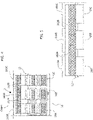
Figure 2 is a plan view of a semiconductor device as discussed herein, -
Figure 3 is a view of the portion ofFigure 2 indicated by arrow III, reproduced on an enlarged scale, -
Figure 4 is a plan view of a semiconductor device as discussed herein, and -
Figure 5 is a view of the portion ofFigure 4 indicated by arrow IV, reproduced on an enlarged scale. - Corresponding numerals and symbols in the different figures generally refer to corresponding parts unless otherwise indicated.
- The figures are drawn to clearly illustrate the relevant aspects of the embodiments and are not necessarily drawn to scale.
- The edges of features drawn in the figures do not necessarily indicate the termination of the extent of the feature.
- In the ensuing description, various specific details are illustrated in order to provide an in-depth understanding of various examples of embodiments according to the description. The embodiments may be obtained without one or more of the specific details, or with other methods, components, materials, etc. In other cases, known structures, materials, or operations are not illustrated or described in detail so that various aspects of the embodiments will not be obscured.
- Reference to "an embodiment" or "one embodiment" in the framework of the present description is intended to indicate that a particular configuration, structure, or characteristic described in relation to the embodiment is comprised in at least one embodiment. Hence, phrases such as "in an embodiment", "in one embodiment", or the like, that may be present in various points of the present description do not necessarily refer exactly to one and the same embodiment. Furthermore, particular configurations, structures, or characteristics may be combined in any adequate way in one or more embodiments.
- The headings/references used herein are provided merely for convenience and hence do not define the extent of protection or the scope of the embodiments.
-
Figures 1A, 1B and 1C are plan views of conventionalsemiconductor power devices 10. - As illustrated, the
devices 10 comprise a substrate such as aleadframe 12 having arranged (attached) thereon one or more semiconductor chips or dice. One of these, indicated as 14, is clearly visible on the left-hand side ofFigures 1A, 1B and 1C . - One or more other chips are only partly visible on the right-hand side of
Figures 1A, 1B and 1C as they are masked by a plurality of "ribbons" 16A, 16B, 16C - three are illustrated by way of example - providing (power) signal propagation paths - The designation "leadframe" (or "lead frame") is currently used (see, for instance the USPC Consolidated Glossary of the United States Patent and Trademark Office) to indicate a metal frame that provides support for an integrated circuit chip or die as well as electrical leads to interconnect the integrated circuit in the die or chip to other electrical components or contacts.
- Leadframes are conventionally created using technologies such as a photo-etching technology. With this technology, metal (e.g., copper) material in the form of a foil or tape is etched on the top and bottom sides to create various pads and leads.
- These technologies can be applied to a Quad-Flat No-leads or QFN packages, where the designation "no-leads" denotes the fact that no leads are provided that protrude radially of the package.
- So-called "pre-molded" leadframes are currently used that include electrically insulating resin such as epoxy resin, for instance, molded onto a sculptured (e.g., photo-etched) leadframe using a flat molding tool, for instance.
- Spaces left in the etched metal material are filled by pre-molding resin and the resulting leadframe has a total thickness that is the same thickness of the original etched leadframe.
- After pre-molding (with the molded resin solidified, via heat or UV curing, for instance), deflashing and smearing processes can be applied to provide clean top/bottom metal surfaces.
- Wettable flanks can be provided, e.g., during a second etching step that can be applied to the pre-molded leadframe to generate dedicated etched areas.
- Also, an insulating encapsulation (an epoxy resin, for instance, not visible in the figures) can be molded onto the
leadframe 12 having the chip(s) 14 and the signal propagation paths orlines - Advantageously (primarily in power applications) signal propagation paths or lines such as the paths or
lines - Unless indicated otherwise in the rest of the present description, examples as discussed in the foregoing are conventional in the art, which makes it unnecessary to provide a more detailed description herein.
- Especially in power applications,
devices 10 capable of being configured with different number of power channels are desirable. - For instance:
- in
Figure 1A , theribbons Ch# 1; - in
Figure 1B , theribbons Ch# 1 and the ribbon 16c is kept electrically separate from theribbons Ch# 2; and - in
Figure 1C , theribbons Ch# 1,Ch# 2, andCh# 3. - In conventional solutions as illustrated in
Figures 1A to 1C these three different arrangements are mirrored by three respective, different leadframe layouts. - From a package perspective, this translates into different types of leadframe designs that take into account the number of channels involved. Such leadframe customization facilitates providing device characteristics as desired to render the final product functional
- From the viewpoint of the supply chain of the components, managing several leadframe versions, some of which may be dedicated just to a small number of products, is largely inconvenient.
- A possible approach in addressing these issues may involve managing the different power channels at board level (e.g., with a printed circuit board or PCB) by bridging the leads with a wire connection.
- For instance, a dual channel package could be shorted at board level to be used as a single channel device via short circuits (jumpers) at board level.
- In such an approach (board customization) the underlying problem of having to manage different leadframe layouts is not properly solved. Rather, the problem is moved or displaced to the board design level, and is thus still present.
- Moreover, board customization is almost invariably carried out by the final customer, which is largely impractical.
- Also, it is noted that, with wire bridging, a new connection is added, involving two welds. This is in contrast with wedge bridging as discussed in the following, which is performed with one weld only.
- Also, wire connection in some cases involves a dedicated area/pad, while a ribbon wedge can be bonded over an existing weld.
- A wedge bonding process utilizes ultrasonic energy and pressure to create a bond. Wedge bonding is thus a low temperature process, where, for example, a wire or ribbon (of aluminum, copper, gold or any other material compatible with ultrasonic bonding) is used to make the interconnection. This process deforms the wire/ribbon into a flat elongated shape of a wedge.
- While wire bonding is already mature in semiconductor industry, bonding a ribbon over different leads and ribbons unexpectedly facilitates customizing power distribution in power packaging.
- Particularly, wedge-on-wedge bridging as exemplified herein can be planned for critical package applications or developments, mostly for power application with the capability of meeting various specifications and flexibility in providing single-channel and multi-channel product versions.
- Examples as discussed herein in connection with figures from
Figure 2 onwards improve leadframe choice flexibility retaining a single multi-channel leadframe layout (e.g., of the type underlying an arrangement as illustrated inFigure 1C , with three independentchannels Ch# 1,Ch# 2, and Ch#3) by coupling (shorting)adjacent ribbons - Examples as discussed herein thus expand on the concept of arranging over a substrate such as a
leadframe 12 one ormore semiconductor chips 14 and a plurality of current-carrying formations such as theribbons ribbons - That is, the substrate or
leadframe 12 ofFigures 2 to 5 is (always) of the type illustrated inFigure 1C , configured to provide threechannels CH# 1,CH# 2, andCH# 3. - In the examples illustrated in
Figures 2 to 5 , at least oneelectrical contact adjacent ribbons adjacent ribbons contact CH# 1. - For instance,
Figures 2 and 3 illustrate a device 10 (not visible in its entirety) where: - two
ribbons wedge 162 welded, e.g., bridge-like between the pins or leads 160A, 160B to form a first current flow path orchannel CH# 1, and - the
third ribbon 16C is maintained distinct at its distal pin or lead 160C to form a second current flow path orchannel CH# 2. -
Figures 2 and 3 are thus exemplary of arranging over the substrate 12 a pair of a first current-carryingformation 16A and a second current-carryingformation 16B, the second current-carryingformation 16B being adjacent the first current-carryingformation 16A. -
Figures 2 and 3 are likewise exemplary of arranging over the substrate 12 a third current-carryingformation 16C adjacent the pair comprised of the first 16A and second 16B current-carrying formations. - As illustrated in
Figures 2 and 3 an electrical contact (wedge) 162 is formed between the pair of the first 16A and second 16B current-carrying formations. - The pair of the first 16A and second 16B current-carrying formations having the
contact 162 formed therebetween are thus coupled to provide a first multi-formation current-carryingchannel CH# 1. - The third current-carrying
formation 16C in turn provides a second single-formation current-carryingchannel CH# 2. - Again, by way of example,
Figures 4 and 5 illustrate a device 10 (again not visible in its entirety) where: - the
ribbons first wedge 162A welded e.g., bridge-like, between the pins or leads 160A and 160B, and - the
ribbons second wedge 162B welded, e.g., bridge-like, between the pins or leads 160B and 160C. - In that way, all of the
ribbons wedges channel CH# 1. -
Figures 4 and 5 are thus exemplary of arranging over the substrate 12 a first current-carryingformation 16A and a second current-carryingformation 16B, the second current-carryingformation 16B adjacent the first current-carryingformation 16A. -
Figures 4 and 5 are likewise exemplary of arranging over the substrate 12 a third current-carryingformation 16C adjacent the second current-carryingformation 16B, and: - forming a first electrical contact (wedge) 162A between the first 16A and second 16B current-carrying formations, and
- forming a second electrical contact (wedge) 162B between the second 16B and third 16C current-carrying formations.
- As illustrated in
Figures 4 and 5 , the first 16A, second 16B, and third 16C current-carrying formations having the first 162A and second 162B contacts formed therebetween are coupled to a single multi-formation current-carrying channel, namelyCH# 1. - While not shown for simplicity, a third possible option involves leaving the
distal pins - In that case, the
ribbons channels CH# 1, CH#2m andCH# 3. - Examples as illustrated herein rely on wedge-on-wedge bridging; this is advantageous in improving the leadframe supply chain, providing selectivity in choosing lead bridging where desired.
- Such wedge-on-wedge bridging can be easily detected thanks to the lead-to-lead connection inside the device package. Detection can be via X-Ray screening or by cross-section and SEM (Scanning Electronic Microscope) picture analysis. X-Ray analysis can be performed sidewise on the whole package body to detect the presence of bridges. Cross-sectional analysis can be performed where the bridge is detected by X-Ray.
- Examples as illustrated herein rely on the possibility of bonding ribbons between two or more leads in order to bridge them. This feature facilitates higher flexibility in leadframe design.
- Examples as illustrated herein improve leadframe choice flexibility by bridging pins through a ribbon bonding process.
- Ribbon bonding as illustrated extends over two neighboring leads, welding a wedge over existing ribbons. Bonding between two adjacent leads facilitates leadframe design standardization and improves product connection customization through connections that can be produced at the assembly level.
- Examples as illustrated herein facilitate achieving a higher bonding flexibility, providing a wider leadframe (LF) choice without compromising on package cost.
- For instance, a same QFN leadframe 12 (devised for a triple channel
application CH# 1,CH# 2, CH#3) can be used for single-channel or two-channel applications too. - It will be appreciated that same concept here exemplified by referring for simplicity to three
ribbons - Bridging two or more of the channels (ribbons) 16A, 16B, and 16C at their
distal ends - It will be otherwise appreciated that bonding two adjacent leads may occur also at other ribbon locations, e.g., at their "proximal" ends adjacent the
circuitry 14 and/or at intermediate points along the length of the ribbons. - Similarly, while in the examples illustrated herein the
contacts contacts - Without prejudice to the underlying principles, the details and embodiments may vary, even significantly, with respect to what has been described in the foregoing, by way of example only, without departing from the extent of protection.
- The extent of protection is determined by the annexed claims.
Claims (12)
- A method, comprising:arranging over a substrate (12) at least one semiconductor chip (14) and a plurality of current-carrying formations (16A, 16B, 16C) coupled to the at least one semiconductor chip (14), wherein the substrate (12) is exempt from electrically conductive formations coupling the current-carrying formations (16A, 16B, 16C) in the plurality of current-carrying formations (16A, 16B, 16C), andforming at least one electrical contact (162; 162A, 162B) between adjacent current-carrying formations (16A, 16B, 16C) in the plurality of current-carrying formations (16A, 16B, 16C), wherein adjacent current-carrying formations (16A, 16B, 16C) having at least one contact (162; 162A, 162B) formed therebetween are coupled into a multi-formation current-carrying channel (CH#1).
- The method of claim 1, comprising:arranging over the substrate (12) a pair of a first current-carrying formation (16A) and a second current-carrying formation (16B), the second current-carrying formation (16B) adjacent the first current-carrying formation (16A),arranging over the substrate (12) a third (16C) current-carrying formation adjacent the pair of first (16A) and second (16B) current-carrying formations (16A, 16B), andforming an electrical contact (162) between the pair of first (16A) and second (16B) current-carrying formations, wherein the pair of first (16A) and second (16B) current-carrying formations having said contact (162) formed therebetween are coupled to a first multi-formation current-carrying channel (CH#1) and the third current-carrying formation (16C) provides a second single-formation current-carrying channel (CH#2).
- The method of claim 1, comprising:arranging over the substrate (12) a first current-carrying formation (16A) and a second current-carrying formation (16B), the second current-carrying formation (16B) adjacent the first current-carrying formation (16A), as well as a third (16C) current-carrying formation adjacent the second current-carrying formation (16B),forming a first electrical contact (162A) between the first (16A) and second (16B) current-carrying formations, andforming a second electrical contact (162B) between the second (16B) and third (16C) current-carrying formations,wherein the first (16A), second (16B), and third (16C) current-carrying formations having said first (162A) and second (162B) contacts formed therebetween are coupled to a single multi-formation current-carrying channel (CH#1).
- The method of any of the previous claims, comprising forming said at least one electrical contact (162; 162A, 162B) between adjacent current-carrying formations (16A, 16B, 16C) in the plurality of current-carrying formations (16A, 16B, 16C) at the distal ends (160A, 160B, 160C) of the current-carrying formations (16A, 16B, 16C) opposite the at least one semiconductor chip 14).
- The method of any of the previous claims, wherein the current-carrying formations (16A, 16B, 16C) comprise electrically conductive ribbons arranged over the substrate (12).
- The method of any of the previous claims comprising forming said at least one electrical contact (162; 162A, 162B) via wedge bonding at said current-carrying formations (16A, 16B, 16C).
- A device (10), comprising:a substrate (12) having arranged thereon at least one semiconductor chip (14) and a plurality of current-carrying formations (16A, 16B, 16C) coupled to the at least one semiconductor chip (14), wherein the substrate (12) is exempt from electrically conductive formations coupling the current-carrying formations (16A, 16B, 16C) in the plurality of current-carrying formations (16A, 16B, 16C), andat least one electrical contact (162; 162A, 162B) between adjacent current-carrying formations (16A, 16B, 16C) in the plurality of current-carrying formations (16A, 16B, 16C), wherein adjacent current-carrying formations (16A, 16B, 16C) having the at least one contact (162; 162A, 162B) therebetween are coupled into a multi-formation current-carrying channel (CH#1).
- The device (10) of claim 7, comprising:a pair of a first current-carrying formation (16A) and a second current-carrying formation (16B) arranged over the substrate (12), the second current-carrying formation (16B) adjacent the first current-carrying formation (16A),a third (16C) current-carrying formation arranged over the substrate (12) adjacent the pair of first (16A) and second (16B) current-carrying formations (16A, 16B), andan electrical contact (162) between the pair of first (16A) and second (16B) current-carrying formations, wherein the pair of first (16A) and second (16B) current-carrying formations having said contact (162) therebetween are coupled to a first multi-formation current-carrying channel (CH#1) and the third current-carrying formation (16C) provides a second single-formation current-carrying channel (CH#2).
- The device (10) of claim 7, comprising:a first current-carrying formation (16A) and a second current-carrying formation (16B) arranged over the substrate (12), the second current-carrying formation (16B) adjacent the first current-carrying formation (16A),a third (16C) current-carrying formation arranged over the substrate (12) adjacent the second current-carrying formation (16B),a first electrical contact (162A) between the first (16A) and second (16B) current-carrying formations, anda second electrical contact (162B) between the second (16B) and third (16C) current-carrying formations,wherein the first (16A), second (16B), and third (16C) current-carrying formations having said first (162A) and second (162B) contacts therebetween are coupled to a single multi-formation current-carrying channel (CH#1).
- The device (10) of any of claims 7 to 9, wherein said at least one electrical contact (162; 162A, 162B) between adjacent current-carrying formations (16A, 16B, 16C) in the plurality of current-carrying formations (16A, 16B, 16C) is at the distal ends (160A, 160B, 160C) of the current-carrying formations (16A, 16B, 16C) opposite the at least one semiconductor chip (14).
- The device (10) of any of claims 7 to 10, wherein the current-carrying formations (16A, 16B, 16C) comprise electrically conductive ribbons arranged over the substrate (12).
- The device (10) of any of claims 7 to 11, said at least one electrical contact (162; 162A, 162B) comprises a wedge bond at said current-carrying formations (16A, 16B, 16C).
Applications Claiming Priority (1)
| Application Number | Priority Date | Filing Date | Title |
|---|---|---|---|
| IT102021000017207A IT202100017207A1 (en) | 2021-06-30 | 2021-06-30 | Process for manufacturing semiconductor devices and corresponding semiconductor device |
Publications (2)
| Publication Number | Publication Date |
|---|---|
| EP4113600A1 true EP4113600A1 (en) | 2023-01-04 |
| EP4113600B1 EP4113600B1 (en) | 2024-04-03 |
Family
ID=77802132
Family Applications (1)
| Application Number | Title | Priority Date | Filing Date |
|---|---|---|---|
| EP22181327.2A Active EP4113600B1 (en) | 2021-06-30 | 2022-06-27 | Method of manufacturing semiconductor devices and corresponding semiconductor device |
Country Status (3)
| Country | Link |
|---|---|
| US (1) | US12406909B2 (en) |
| EP (1) | EP4113600B1 (en) |
| IT (1) | IT202100017207A1 (en) |
Families Citing this family (2)
| Publication number | Priority date | Publication date | Assignee | Title |
|---|---|---|---|---|
| US12575468B2 (en) * | 2021-10-07 | 2026-03-10 | Stmicroelectronics S.R.L. | Roughened surface of a conductive wedge bonded ribbon encapsulated in a sermiconductor package |
| IT202300017700A1 (en) * | 2023-08-29 | 2025-03-01 | St Microelectronics Int Nv | PROCEDURE FOR MANUFACTURING SEMICONDUCTOR DEVICES, COMPONENT AND CORRESPONDING SEMICONDUCTOR DEVICE |
Citations (3)
| Publication number | Priority date | Publication date | Assignee | Title |
|---|---|---|---|---|
| US20070108601A1 (en) * | 2005-11-09 | 2007-05-17 | Stats Chippac Ltd. | Integrated circuit package system including ribbon bond interconnect |
| US20150187684A1 (en) * | 2013-12-26 | 2015-07-02 | Samsung Electro-Mechanics Co., Ltd. | Semiconductor package |
| US20200176371A1 (en) * | 2018-11-30 | 2020-06-04 | Rohm Co., Ltd. | Semiconductor device |
Family Cites Families (5)
| Publication number | Priority date | Publication date | Assignee | Title |
|---|---|---|---|---|
| US8450149B2 (en) | 2009-10-16 | 2013-05-28 | Texas Instruments Incorporated | Stacked leadframe implementation for DC/DC convertor power module incorporating a stacked controller and stacked leadframe construction methodology |
| US20120326287A1 (en) | 2011-06-27 | 2012-12-27 | National Semiconductor Corporation | Dc/dc convertor power module package incorporating a stacked controller and construction methodology |
| US20110147928A1 (en) | 2009-12-22 | 2011-06-23 | Tessera Research Llc | Microelectronic assembly with bond elements having lowered inductance |
| EP3761359B1 (en) | 2019-07-03 | 2025-04-30 | Nexperia B.V. | A lead frame assembly for a semiconductor device |
| CN115547841A (en) | 2021-06-30 | 2022-12-30 | 意法半导体股份有限公司 | Method for manufacturing semiconductor device and corresponding semiconductor device |
-
2021
- 2021-06-30 IT IT102021000017207A patent/IT202100017207A1/en unknown
-
2022
- 2022-06-24 US US17/848,958 patent/US12406909B2/en active Active
- 2022-06-27 EP EP22181327.2A patent/EP4113600B1/en active Active
Patent Citations (3)
| Publication number | Priority date | Publication date | Assignee | Title |
|---|---|---|---|---|
| US20070108601A1 (en) * | 2005-11-09 | 2007-05-17 | Stats Chippac Ltd. | Integrated circuit package system including ribbon bond interconnect |
| US20150187684A1 (en) * | 2013-12-26 | 2015-07-02 | Samsung Electro-Mechanics Co., Ltd. | Semiconductor package |
| US20200176371A1 (en) * | 2018-11-30 | 2020-06-04 | Rohm Co., Ltd. | Semiconductor device |
Also Published As
| Publication number | Publication date |
|---|---|
| US20230005826A1 (en) | 2023-01-05 |
| IT202100017207A1 (en) | 2022-12-30 |
| EP4113600B1 (en) | 2024-04-03 |
| US12406909B2 (en) | 2025-09-02 |
Similar Documents
| Publication | Publication Date | Title |
|---|---|---|
| US8704342B2 (en) | Resin sealing type semiconductor device and method of manufacturing the same, and lead frame | |
| US6066515A (en) | Multilevel leadframe for a packaged integrated circuit | |
| US6930380B2 (en) | Semiconductor device | |
| EP4113600B1 (en) | Method of manufacturing semiconductor devices and corresponding semiconductor device | |
| US6979886B2 (en) | Short-prevented lead frame and method for fabricating semiconductor package with the same | |
| CN218123353U (en) | Semiconductor device | |
| CN107104054A (en) | Packaging structure | |
| US12506053B2 (en) | Method of assembling semiconductor devices and corresponding semiconductor device | |
| US20230005824A1 (en) | Method of manufacturing substrates for semiconductor devices, corresponding substrate and semiconductor device | |
| US12463170B2 (en) | Semiconductor device and assortment of semiconductor devices with electrically conductive ribbon configurations | |
| EP4016617A1 (en) | Method of manufacturing semiconductor devices, component for use therein and corresponding semiconductor device | |
| JP6143726B2 (en) | Resin-encapsulated semiconductor device, manufacturing method thereof, lead frame | |
| US20250079386A1 (en) | Method of manufacturing semiconductor devices, corresponding component and semiconductor device | |
| US20240145351A1 (en) | Method of manufacturing semiconductor devices, corresponding semiconductor device, assembly and support substrate | |
| EP4411814A1 (en) | Method of manufacturing semiconductor devices, corresponding ribbon, apparatus and device | |
| US20250014982A1 (en) | Method of manufacturing semiconductor devices, corresponding pre-molded leadframe and semiconductor device | |
| JP5145596B2 (en) | Semiconductor device | |
| JP2005142284A (en) | Semiconductor device | |
| JP2002164496A (en) | Semiconductor device and manufacturing method thereof | |
| KR970005721B1 (en) | Lead frame | |
| JP2000183271A (en) | Lead frame, semiconductor device, and method of manufacturing semiconductor device | |
| KR20020030174A (en) | structure of lead frame for fabrication of semiconductor |
Legal Events
| Date | Code | Title | Description |
|---|---|---|---|
| PUAI | Public reference made under article 153(3) epc to a published international application that has entered the european phase |
Free format text: ORIGINAL CODE: 0009012 |
|
| STAA | Information on the status of an ep patent application or granted ep patent |
Free format text: STATUS: THE APPLICATION HAS BEEN PUBLISHED |
|
| AK | Designated contracting states |
Kind code of ref document: A1 Designated state(s): AL AT BE BG CH CY CZ DE DK EE ES FI FR GB GR HR HU IE IS IT LI LT LU LV MC MK MT NL NO PL PT RO RS SE SI SK SM TR |
|
| STAA | Information on the status of an ep patent application or granted ep patent |
Free format text: STATUS: REQUEST FOR EXAMINATION WAS MADE |
|
| 17P | Request for examination filed |
Effective date: 20230607 |
|
| RBV | Designated contracting states (corrected) |
Designated state(s): AL AT BE BG CH CY CZ DE DK EE ES FI FR GB GR HR HU IE IS IT LI LT LU LV MC MK MT NL NO PL PT RO RS SE SI SK SM TR |
|
| GRAP | Despatch of communication of intention to grant a patent |
Free format text: ORIGINAL CODE: EPIDOSNIGR1 |
|
| STAA | Information on the status of an ep patent application or granted ep patent |
Free format text: STATUS: GRANT OF PATENT IS INTENDED |
|
| INTG | Intention to grant announced |
Effective date: 20231031 |
|
| GRAS | Grant fee paid |
Free format text: ORIGINAL CODE: EPIDOSNIGR3 |
|
| GRAA | (expected) grant |
Free format text: ORIGINAL CODE: 0009210 |
|
| STAA | Information on the status of an ep patent application or granted ep patent |
Free format text: STATUS: THE PATENT HAS BEEN GRANTED |
|
| AK | Designated contracting states |
Kind code of ref document: B1 Designated state(s): AL AT BE BG CH CY CZ DE DK EE ES FI FR GB GR HR HU IE IS IT LI LT LU LV MC MK MT NL NO PL PT RO RS SE SI SK SM TR |
|
| REG | Reference to a national code |
Ref country code: CH Ref legal event code: EP |
|
| REG | Reference to a national code |
Ref country code: DE Ref legal event code: R096 Ref document number: 602022002664 Country of ref document: DE |
|
| REG | Reference to a national code |
Ref country code: IE Ref legal event code: FG4D |
|
| REG | Reference to a national code |
Ref country code: LT Ref legal event code: MG9D |
|
| REG | Reference to a national code |
Ref country code: NL Ref legal event code: MP Effective date: 20240403 |
|
| REG | Reference to a national code |
Ref country code: AT Ref legal event code: MK05 Ref document number: 1673357 Country of ref document: AT Kind code of ref document: T Effective date: 20240403 |
|
| PG25 | Lapsed in a contracting state [announced via postgrant information from national office to epo] |
Ref country code: NL Free format text: LAPSE BECAUSE OF FAILURE TO SUBMIT A TRANSLATION OF THE DESCRIPTION OR TO PAY THE FEE WITHIN THE PRESCRIBED TIME-LIMIT Effective date: 20240403 |
|
| PG25 | Lapsed in a contracting state [announced via postgrant information from national office to epo] |
Ref country code: NL Free format text: LAPSE BECAUSE OF FAILURE TO SUBMIT A TRANSLATION OF THE DESCRIPTION OR TO PAY THE FEE WITHIN THE PRESCRIBED TIME-LIMIT Effective date: 20240403 |
|
| PG25 | Lapsed in a contracting state [announced via postgrant information from national office to epo] |
Ref country code: IS Free format text: LAPSE BECAUSE OF FAILURE TO SUBMIT A TRANSLATION OF THE DESCRIPTION OR TO PAY THE FEE WITHIN THE PRESCRIBED TIME-LIMIT Effective date: 20240803 |
|
| PG25 | Lapsed in a contracting state [announced via postgrant information from national office to epo] |
Ref country code: BG Free format text: LAPSE BECAUSE OF FAILURE TO SUBMIT A TRANSLATION OF THE DESCRIPTION OR TO PAY THE FEE WITHIN THE PRESCRIBED TIME-LIMIT Effective date: 20240403 |
|
| PG25 | Lapsed in a contracting state [announced via postgrant information from national office to epo] |
Ref country code: HR Free format text: LAPSE BECAUSE OF FAILURE TO SUBMIT A TRANSLATION OF THE DESCRIPTION OR TO PAY THE FEE WITHIN THE PRESCRIBED TIME-LIMIT Effective date: 20240403 Ref country code: FI Free format text: LAPSE BECAUSE OF FAILURE TO SUBMIT A TRANSLATION OF THE DESCRIPTION OR TO PAY THE FEE WITHIN THE PRESCRIBED TIME-LIMIT Effective date: 20240403 |
|
| PG25 | Lapsed in a contracting state [announced via postgrant information from national office to epo] |
Ref country code: GR Free format text: LAPSE BECAUSE OF FAILURE TO SUBMIT A TRANSLATION OF THE DESCRIPTION OR TO PAY THE FEE WITHIN THE PRESCRIBED TIME-LIMIT Effective date: 20240704 |
|
| PG25 | Lapsed in a contracting state [announced via postgrant information from national office to epo] |
Ref country code: PT Free format text: LAPSE BECAUSE OF FAILURE TO SUBMIT A TRANSLATION OF THE DESCRIPTION OR TO PAY THE FEE WITHIN THE PRESCRIBED TIME-LIMIT Effective date: 20240805 |
|
| PG25 | Lapsed in a contracting state [announced via postgrant information from national office to epo] |
Ref country code: ES Free format text: LAPSE BECAUSE OF FAILURE TO SUBMIT A TRANSLATION OF THE DESCRIPTION OR TO PAY THE FEE WITHIN THE PRESCRIBED TIME-LIMIT Effective date: 20240403 |
|
| PG25 | Lapsed in a contracting state [announced via postgrant information from national office to epo] |
Ref country code: CZ Free format text: LAPSE BECAUSE OF FAILURE TO SUBMIT A TRANSLATION OF THE DESCRIPTION OR TO PAY THE FEE WITHIN THE PRESCRIBED TIME-LIMIT Effective date: 20240403 |
|
| PG25 | Lapsed in a contracting state [announced via postgrant information from national office to epo] |
Ref country code: AT Free format text: LAPSE BECAUSE OF FAILURE TO SUBMIT A TRANSLATION OF THE DESCRIPTION OR TO PAY THE FEE WITHIN THE PRESCRIBED TIME-LIMIT Effective date: 20240403 |
|
| PG25 | Lapsed in a contracting state [announced via postgrant information from national office to epo] |
Ref country code: PL Free format text: LAPSE BECAUSE OF FAILURE TO SUBMIT A TRANSLATION OF THE DESCRIPTION OR TO PAY THE FEE WITHIN THE PRESCRIBED TIME-LIMIT Effective date: 20240403 |
|
| PG25 | Lapsed in a contracting state [announced via postgrant information from national office to epo] |
Ref country code: LV Free format text: LAPSE BECAUSE OF FAILURE TO SUBMIT A TRANSLATION OF THE DESCRIPTION OR TO PAY THE FEE WITHIN THE PRESCRIBED TIME-LIMIT Effective date: 20240403 |
|
| PG25 | Lapsed in a contracting state [announced via postgrant information from national office to epo] |
Ref country code: PT Free format text: LAPSE BECAUSE OF FAILURE TO SUBMIT A TRANSLATION OF THE DESCRIPTION OR TO PAY THE FEE WITHIN THE PRESCRIBED TIME-LIMIT Effective date: 20240805 Ref country code: PL Free format text: LAPSE BECAUSE OF FAILURE TO SUBMIT A TRANSLATION OF THE DESCRIPTION OR TO PAY THE FEE WITHIN THE PRESCRIBED TIME-LIMIT Effective date: 20240403 Ref country code: NO Free format text: LAPSE BECAUSE OF FAILURE TO SUBMIT A TRANSLATION OF THE DESCRIPTION OR TO PAY THE FEE WITHIN THE PRESCRIBED TIME-LIMIT Effective date: 20240703 Ref country code: LV Free format text: LAPSE BECAUSE OF FAILURE TO SUBMIT A TRANSLATION OF THE DESCRIPTION OR TO PAY THE FEE WITHIN THE PRESCRIBED TIME-LIMIT Effective date: 20240403 Ref country code: IS Free format text: LAPSE BECAUSE OF FAILURE TO SUBMIT A TRANSLATION OF THE DESCRIPTION OR TO PAY THE FEE WITHIN THE PRESCRIBED TIME-LIMIT Effective date: 20240803 Ref country code: HR Free format text: LAPSE BECAUSE OF FAILURE TO SUBMIT A TRANSLATION OF THE DESCRIPTION OR TO PAY THE FEE WITHIN THE PRESCRIBED TIME-LIMIT Effective date: 20240403 Ref country code: GR Free format text: LAPSE BECAUSE OF FAILURE TO SUBMIT A TRANSLATION OF THE DESCRIPTION OR TO PAY THE FEE WITHIN THE PRESCRIBED TIME-LIMIT Effective date: 20240704 Ref country code: FI Free format text: LAPSE BECAUSE OF FAILURE TO SUBMIT A TRANSLATION OF THE DESCRIPTION OR TO PAY THE FEE WITHIN THE PRESCRIBED TIME-LIMIT Effective date: 20240403 Ref country code: ES Free format text: LAPSE BECAUSE OF FAILURE TO SUBMIT A TRANSLATION OF THE DESCRIPTION OR TO PAY THE FEE WITHIN THE PRESCRIBED TIME-LIMIT Effective date: 20240403 Ref country code: CZ Free format text: LAPSE BECAUSE OF FAILURE TO SUBMIT A TRANSLATION OF THE DESCRIPTION OR TO PAY THE FEE WITHIN THE PRESCRIBED TIME-LIMIT Effective date: 20240403 Ref country code: BG Free format text: LAPSE BECAUSE OF FAILURE TO SUBMIT A TRANSLATION OF THE DESCRIPTION OR TO PAY THE FEE WITHIN THE PRESCRIBED TIME-LIMIT Effective date: 20240403 Ref country code: AT Free format text: LAPSE BECAUSE OF FAILURE TO SUBMIT A TRANSLATION OF THE DESCRIPTION OR TO PAY THE FEE WITHIN THE PRESCRIBED TIME-LIMIT Effective date: 20240403 Ref country code: RS Free format text: LAPSE BECAUSE OF FAILURE TO SUBMIT A TRANSLATION OF THE DESCRIPTION OR TO PAY THE FEE WITHIN THE PRESCRIBED TIME-LIMIT Effective date: 20240703 |
|
| REG | Reference to a national code |
Ref country code: DE Ref legal event code: R097 Ref document number: 602022002664 Country of ref document: DE |
|
| PG25 | Lapsed in a contracting state [announced via postgrant information from national office to epo] |
Ref country code: DK Free format text: LAPSE BECAUSE OF FAILURE TO SUBMIT A TRANSLATION OF THE DESCRIPTION OR TO PAY THE FEE WITHIN THE PRESCRIBED TIME-LIMIT Effective date: 20240403 |
|
| PG25 | Lapsed in a contracting state [announced via postgrant information from national office to epo] |
Ref country code: EE Free format text: LAPSE BECAUSE OF FAILURE TO SUBMIT A TRANSLATION OF THE DESCRIPTION OR TO PAY THE FEE WITHIN THE PRESCRIBED TIME-LIMIT Effective date: 20240403 |
|
| PG25 | Lapsed in a contracting state [announced via postgrant information from national office to epo] |
Ref country code: RO Free format text: LAPSE BECAUSE OF FAILURE TO SUBMIT A TRANSLATION OF THE DESCRIPTION OR TO PAY THE FEE WITHIN THE PRESCRIBED TIME-LIMIT Effective date: 20240403 Ref country code: SK Free format text: LAPSE BECAUSE OF FAILURE TO SUBMIT A TRANSLATION OF THE DESCRIPTION OR TO PAY THE FEE WITHIN THE PRESCRIBED TIME-LIMIT Effective date: 20240403 |
|
| PG25 | Lapsed in a contracting state [announced via postgrant information from national office to epo] |
Ref country code: SM Free format text: LAPSE BECAUSE OF FAILURE TO SUBMIT A TRANSLATION OF THE DESCRIPTION OR TO PAY THE FEE WITHIN THE PRESCRIBED TIME-LIMIT Effective date: 20240403 |
|
| PG25 | Lapsed in a contracting state [announced via postgrant information from national office to epo] |
Ref country code: SM Free format text: LAPSE BECAUSE OF FAILURE TO SUBMIT A TRANSLATION OF THE DESCRIPTION OR TO PAY THE FEE WITHIN THE PRESCRIBED TIME-LIMIT Effective date: 20240403 Ref country code: SK Free format text: LAPSE BECAUSE OF FAILURE TO SUBMIT A TRANSLATION OF THE DESCRIPTION OR TO PAY THE FEE WITHIN THE PRESCRIBED TIME-LIMIT Effective date: 20240403 Ref country code: RO Free format text: LAPSE BECAUSE OF FAILURE TO SUBMIT A TRANSLATION OF THE DESCRIPTION OR TO PAY THE FEE WITHIN THE PRESCRIBED TIME-LIMIT Effective date: 20240403 Ref country code: EE Free format text: LAPSE BECAUSE OF FAILURE TO SUBMIT A TRANSLATION OF THE DESCRIPTION OR TO PAY THE FEE WITHIN THE PRESCRIBED TIME-LIMIT Effective date: 20240403 Ref country code: DK Free format text: LAPSE BECAUSE OF FAILURE TO SUBMIT A TRANSLATION OF THE DESCRIPTION OR TO PAY THE FEE WITHIN THE PRESCRIBED TIME-LIMIT Effective date: 20240403 Ref country code: MC Free format text: LAPSE BECAUSE OF FAILURE TO SUBMIT A TRANSLATION OF THE DESCRIPTION OR TO PAY THE FEE WITHIN THE PRESCRIBED TIME-LIMIT Effective date: 20240403 |
|
| PLBE | No opposition filed within time limit |
Free format text: ORIGINAL CODE: 0009261 |
|
| STAA | Information on the status of an ep patent application or granted ep patent |
Free format text: STATUS: NO OPPOSITION FILED WITHIN TIME LIMIT |
|
| PG25 | Lapsed in a contracting state [announced via postgrant information from national office to epo] |
Ref country code: LU Free format text: LAPSE BECAUSE OF NON-PAYMENT OF DUE FEES Effective date: 20240627 |
|
| 26N | No opposition filed |
Effective date: 20250106 |
|
| PG25 | Lapsed in a contracting state [announced via postgrant information from national office to epo] |
Ref country code: IE Free format text: LAPSE BECAUSE OF NON-PAYMENT OF DUE FEES Effective date: 20240627 |
|
| PG25 | Lapsed in a contracting state [announced via postgrant information from national office to epo] |
Ref country code: SI Free format text: LAPSE BECAUSE OF FAILURE TO SUBMIT A TRANSLATION OF THE DESCRIPTION OR TO PAY THE FEE WITHIN THE PRESCRIBED TIME-LIMIT Effective date: 20240403 Ref country code: BE Free format text: LAPSE BECAUSE OF NON-PAYMENT OF DUE FEES Effective date: 20240630 |
|
| PG25 | Lapsed in a contracting state [announced via postgrant information from national office to epo] |
Ref country code: FR Free format text: LAPSE BECAUSE OF NON-PAYMENT OF DUE FEES Effective date: 20240630 |
|
| REG | Reference to a national code |
Ref country code: BE Ref legal event code: MM Effective date: 20240630 |
|
| PGFP | Annual fee paid to national office [announced via postgrant information from national office to epo] |
Ref country code: DE Payment date: 20250520 Year of fee payment: 4 |
|
| PG25 | Lapsed in a contracting state [announced via postgrant information from national office to epo] |
Ref country code: SE Free format text: LAPSE BECAUSE OF FAILURE TO SUBMIT A TRANSLATION OF THE DESCRIPTION OR TO PAY THE FEE WITHIN THE PRESCRIBED TIME-LIMIT Effective date: 20240403 |
|
| PG25 | Lapsed in a contracting state [announced via postgrant information from national office to epo] |
Ref country code: CY Free format text: LAPSE BECAUSE OF FAILURE TO SUBMIT A TRANSLATION OF THE DESCRIPTION OR TO PAY THE FEE WITHIN THE PRESCRIBED TIME-LIMIT; INVALID AB INITIO Effective date: 20220627 |
|
| REG | Reference to a national code |
Ref country code: DE Ref legal event code: R079 Ref document number: 602022002664 Country of ref document: DE Free format text: PREVIOUS MAIN CLASS: H01L0023495000 Ipc: H10W0070400000 |
|
| REG | Reference to a national code |
Ref country code: CH Ref legal event code: H13 Free format text: ST27 STATUS EVENT CODE: U-0-0-H10-H13 (AS PROVIDED BY THE NATIONAL OFFICE) Effective date: 20260127 |
|
| PG25 | Lapsed in a contracting state [announced via postgrant information from national office to epo] |
Ref country code: IT Free format text: LAPSE BECAUSE OF FAILURE TO SUBMIT A TRANSLATION OF THE DESCRIPTION OR TO PAY THE FEE WITHIN THE PRESCRIBED TIME-LIMIT Effective date: 20240403 |
|
| PG25 | Lapsed in a contracting state [announced via postgrant information from national office to epo] |
Ref country code: HU Free format text: LAPSE BECAUSE OF FAILURE TO SUBMIT A TRANSLATION OF THE DESCRIPTION OR TO PAY THE FEE WITHIN THE PRESCRIBED TIME-LIMIT; INVALID AB INITIO Effective date: 20220627 |
|
| PG25 | Lapsed in a contracting state [announced via postgrant information from national office to epo] |
Ref country code: CH Free format text: LAPSE BECAUSE OF NON-PAYMENT OF DUE FEES Effective date: 20250630 |