EP4113598A2 - Integrated electronic device with a pad structure including a barrier structure and related manufacturing process - Google Patents
Integrated electronic device with a pad structure including a barrier structure and related manufacturing process Download PDFInfo
- Publication number
- EP4113598A2 EP4113598A2 EP22181496.5A EP22181496A EP4113598A2 EP 4113598 A2 EP4113598 A2 EP 4113598A2 EP 22181496 A EP22181496 A EP 22181496A EP 4113598 A2 EP4113598 A2 EP 4113598A2
- Authority
- EP
- European Patent Office
- Prior art keywords
- region
- aperture
- barrier structure
- conductive region
- electronic device
- Prior art date
- Legal status (The legal status is an assumption and is not a legal conclusion. Google has not performed a legal analysis and makes no representation as to the accuracy of the status listed.)
- Withdrawn
Links
Images


Classifications
-
- H—ELECTRICITY
- H10—SEMICONDUCTOR DEVICES; ELECTRIC SOLID-STATE DEVICES NOT OTHERWISE PROVIDED FOR
- H10W—GENERIC PACKAGES, INTERCONNECTIONS, CONNECTORS OR OTHER CONSTRUCTIONAL DETAILS OF DEVICES COVERED BY CLASS H10
- H10W20/00—Interconnections in chips, wafers or substrates
- H10W20/01—Manufacture or treatment
- H10W20/031—Manufacture or treatment of conductive parts of the interconnections
- H10W20/032—Manufacture or treatment of conductive parts of the interconnections of conductive barrier, adhesion or liner layers
- H10W20/038—Manufacture or treatment of conductive parts of the interconnections of conductive barrier, adhesion or liner layers covering conductive structures
-
- H—ELECTRICITY
- H10—SEMICONDUCTOR DEVICES; ELECTRIC SOLID-STATE DEVICES NOT OTHERWISE PROVIDED FOR
- H10P—GENERIC PROCESSES OR APPARATUS FOR THE MANUFACTURE OR TREATMENT OF DEVICES COVERED BY CLASS H10
- H10P14/00—Formation of materials, e.g. in the shape of layers or pillars
- H10P14/40—Formation of materials, e.g. in the shape of layers or pillars of conductive or resistive materials
-
- H—ELECTRICITY
- H10—SEMICONDUCTOR DEVICES; ELECTRIC SOLID-STATE DEVICES NOT OTHERWISE PROVIDED FOR
- H10W—GENERIC PACKAGES, INTERCONNECTIONS, CONNECTORS OR OTHER CONSTRUCTIONAL DETAILS OF DEVICES COVERED BY CLASS H10
- H10W20/00—Interconnections in chips, wafers or substrates
- H10W20/01—Manufacture or treatment
- H10W20/031—Manufacture or treatment of conductive parts of the interconnections
- H10W20/032—Manufacture or treatment of conductive parts of the interconnections of conductive barrier, adhesion or liner layers
- H10W20/033—Manufacture or treatment of conductive parts of the interconnections of conductive barrier, adhesion or liner layers in openings in dielectrics
-
- H—ELECTRICITY
- H10—SEMICONDUCTOR DEVICES; ELECTRIC SOLID-STATE DEVICES NOT OTHERWISE PROVIDED FOR
- H10W—GENERIC PACKAGES, INTERCONNECTIONS, CONNECTORS OR OTHER CONSTRUCTIONAL DETAILS OF DEVICES COVERED BY CLASS H10
- H10W20/00—Interconnections in chips, wafers or substrates
- H10W20/01—Manufacture or treatment
- H10W20/031—Manufacture or treatment of conductive parts of the interconnections
- H10W20/032—Manufacture or treatment of conductive parts of the interconnections of conductive barrier, adhesion or liner layers
- H10W20/054—Manufacture or treatment of conductive parts of the interconnections of conductive barrier, adhesion or liner layers by selectively removing parts thereof
-
- H—ELECTRICITY
- H10—SEMICONDUCTOR DEVICES; ELECTRIC SOLID-STATE DEVICES NOT OTHERWISE PROVIDED FOR
- H10W—GENERIC PACKAGES, INTERCONNECTIONS, CONNECTORS OR OTHER CONSTRUCTIONAL DETAILS OF DEVICES COVERED BY CLASS H10
- H10W20/00—Interconnections in chips, wafers or substrates
- H10W20/40—Interconnections external to wafers or substrates, e.g. back-end-of-line [BEOL] metallisations or vias connecting to gate electrodes
- H10W20/41—Interconnections external to wafers or substrates, e.g. back-end-of-line [BEOL] metallisations or vias connecting to gate electrodes characterised by their conductive parts
- H10W20/44—Conductive materials thereof
- H10W20/4403—Conductive materials thereof based on metals, e.g. alloys, metal silicides
-
- H—ELECTRICITY
- H10—SEMICONDUCTOR DEVICES; ELECTRIC SOLID-STATE DEVICES NOT OTHERWISE PROVIDED FOR
- H10W—GENERIC PACKAGES, INTERCONNECTIONS, CONNECTORS OR OTHER CONSTRUCTIONAL DETAILS OF DEVICES COVERED BY CLASS H10
- H10W42/00—Arrangements for protection of devices
-
- H—ELECTRICITY
- H10—SEMICONDUCTOR DEVICES; ELECTRIC SOLID-STATE DEVICES NOT OTHERWISE PROVIDED FOR
- H10W—GENERIC PACKAGES, INTERCONNECTIONS, CONNECTORS OR OTHER CONSTRUCTIONAL DETAILS OF DEVICES COVERED BY CLASS H10
- H10W20/00—Interconnections in chips, wafers or substrates
- H10W20/01—Manufacture or treatment
- H10W20/031—Manufacture or treatment of conductive parts of the interconnections
- H10W20/032—Manufacture or treatment of conductive parts of the interconnections of conductive barrier, adhesion or liner layers
- H10W20/0375—Manufacture or treatment of conductive parts of the interconnections of conductive barrier, adhesion or liner layers comprising multiple stacked thin barrier, adhesion or liner layers not being formed in openings in dielectrics
-
- H—ELECTRICITY
- H10—SEMICONDUCTOR DEVICES; ELECTRIC SOLID-STATE DEVICES NOT OTHERWISE PROVIDED FOR
- H10W—GENERIC PACKAGES, INTERCONNECTIONS, CONNECTORS OR OTHER CONSTRUCTIONAL DETAILS OF DEVICES COVERED BY CLASS H10
- H10W72/00—Interconnections or connectors in packages
- H10W72/01—Manufacture or treatment
- H10W72/019—Manufacture or treatment of bond pads
- H10W72/01931—Manufacture or treatment of bond pads using blanket deposition
- H10W72/01933—Manufacture or treatment of bond pads using blanket deposition in liquid form, e.g. spin coating, spray coating or immersion coating
- H10W72/01935—Manufacture or treatment of bond pads using blanket deposition in liquid form, e.g. spin coating, spray coating or immersion coating by plating, e.g. electroless plating or electroplating
-
- H—ELECTRICITY
- H10—SEMICONDUCTOR DEVICES; ELECTRIC SOLID-STATE DEVICES NOT OTHERWISE PROVIDED FOR
- H10W—GENERIC PACKAGES, INTERCONNECTIONS, CONNECTORS OR OTHER CONSTRUCTIONAL DETAILS OF DEVICES COVERED BY CLASS H10
- H10W72/00—Interconnections or connectors in packages
- H10W72/01—Manufacture or treatment
- H10W72/019—Manufacture or treatment of bond pads
- H10W72/01951—Changing the shapes of bond pads
- H10W72/01955—Changing the shapes of bond pads by using masks
-
- H—ELECTRICITY
- H10—SEMICONDUCTOR DEVICES; ELECTRIC SOLID-STATE DEVICES NOT OTHERWISE PROVIDED FOR
- H10W—GENERIC PACKAGES, INTERCONNECTIONS, CONNECTORS OR OTHER CONSTRUCTIONAL DETAILS OF DEVICES COVERED BY CLASS H10
- H10W72/00—Interconnections or connectors in packages
- H10W72/50—Bond wires
- H10W72/59—Bond pads specially adapted therefor
-
- H—ELECTRICITY
- H10—SEMICONDUCTOR DEVICES; ELECTRIC SOLID-STATE DEVICES NOT OTHERWISE PROVIDED FOR
- H10W—GENERIC PACKAGES, INTERCONNECTIONS, CONNECTORS OR OTHER CONSTRUCTIONAL DETAILS OF DEVICES COVERED BY CLASS H10
- H10W72/00—Interconnections or connectors in packages
- H10W72/90—Bond pads, in general
- H10W72/921—Structures or relative sizes of bond pads
- H10W72/923—Bond pads having multiple stacked layers
-
- H—ELECTRICITY
- H10—SEMICONDUCTOR DEVICES; ELECTRIC SOLID-STATE DEVICES NOT OTHERWISE PROVIDED FOR
- H10W—GENERIC PACKAGES, INTERCONNECTIONS, CONNECTORS OR OTHER CONSTRUCTIONAL DETAILS OF DEVICES COVERED BY CLASS H10
- H10W72/00—Interconnections or connectors in packages
- H10W72/90—Bond pads, in general
- H10W72/931—Shapes of bond pads
- H10W72/932—Plan-view shape, i.e. in top view
-
- H—ELECTRICITY
- H10—SEMICONDUCTOR DEVICES; ELECTRIC SOLID-STATE DEVICES NOT OTHERWISE PROVIDED FOR
- H10W—GENERIC PACKAGES, INTERCONNECTIONS, CONNECTORS OR OTHER CONSTRUCTIONAL DETAILS OF DEVICES COVERED BY CLASS H10
- H10W72/00—Interconnections or connectors in packages
- H10W72/90—Bond pads, in general
- H10W72/931—Shapes of bond pads
- H10W72/934—Cross-sectional shape, i.e. in side view
-
- H—ELECTRICITY
- H10—SEMICONDUCTOR DEVICES; ELECTRIC SOLID-STATE DEVICES NOT OTHERWISE PROVIDED FOR
- H10W—GENERIC PACKAGES, INTERCONNECTIONS, CONNECTORS OR OTHER CONSTRUCTIONAL DETAILS OF DEVICES COVERED BY CLASS H10
- H10W72/00—Interconnections or connectors in packages
- H10W72/90—Bond pads, in general
- H10W72/941—Dispositions of bond pads
- H10W72/9415—Dispositions of bond pads relative to the surface, e.g. recessed, protruding
-
- H—ELECTRICITY
- H10—SEMICONDUCTOR DEVICES; ELECTRIC SOLID-STATE DEVICES NOT OTHERWISE PROVIDED FOR
- H10W—GENERIC PACKAGES, INTERCONNECTIONS, CONNECTORS OR OTHER CONSTRUCTIONAL DETAILS OF DEVICES COVERED BY CLASS H10
- H10W72/00—Interconnections or connectors in packages
- H10W72/90—Bond pads, in general
- H10W72/941—Dispositions of bond pads
- H10W72/942—Dispositions of bond pads relative to underlying supporting features, e.g. bond pads, RDLs or vias
-
- H—ELECTRICITY
- H10—SEMICONDUCTOR DEVICES; ELECTRIC SOLID-STATE DEVICES NOT OTHERWISE PROVIDED FOR
- H10W—GENERIC PACKAGES, INTERCONNECTIONS, CONNECTORS OR OTHER CONSTRUCTIONAL DETAILS OF DEVICES COVERED BY CLASS H10
- H10W72/00—Interconnections or connectors in packages
- H10W72/90—Bond pads, in general
- H10W72/951—Materials of bond pads
- H10W72/952—Materials of bond pads comprising metals or metalloids, e.g. PbSn, Ag or Cu
-
- H—ELECTRICITY
- H10—SEMICONDUCTOR DEVICES; ELECTRIC SOLID-STATE DEVICES NOT OTHERWISE PROVIDED FOR
- H10W—GENERIC PACKAGES, INTERCONNECTIONS, CONNECTORS OR OTHER CONSTRUCTIONAL DETAILS OF DEVICES COVERED BY CLASS H10
- H10W72/00—Interconnections or connectors in packages
- H10W72/90—Bond pads, in general
- H10W72/981—Auxiliary members, e.g. spacers
-
- H—ELECTRICITY
- H10—SEMICONDUCTOR DEVICES; ELECTRIC SOLID-STATE DEVICES NOT OTHERWISE PROVIDED FOR
- H10W—GENERIC PACKAGES, INTERCONNECTIONS, CONNECTORS OR OTHER CONSTRUCTIONAL DETAILS OF DEVICES COVERED BY CLASS H10
- H10W72/00—Interconnections or connectors in packages
- H10W72/90—Bond pads, in general
- H10W72/981—Auxiliary members, e.g. spacers
- H10W72/983—Reinforcing structures, e.g. collars
-
- H—ELECTRICITY
- H10—SEMICONDUCTOR DEVICES; ELECTRIC SOLID-STATE DEVICES NOT OTHERWISE PROVIDED FOR
- H10W—GENERIC PACKAGES, INTERCONNECTIONS, CONNECTORS OR OTHER CONSTRUCTIONAL DETAILS OF DEVICES COVERED BY CLASS H10
- H10W74/00—Encapsulations, e.g. protective coatings
- H10W74/10—Encapsulations, e.g. protective coatings characterised by their shape or disposition
- H10W74/131—Encapsulations, e.g. protective coatings characterised by their shape or disposition the semiconductor body being only partially enclosed
- H10W74/137—Encapsulations, e.g. protective coatings characterised by their shape or disposition the semiconductor body being only partially enclosed the encapsulations being directly on the semiconductor body
-
- H—ELECTRICITY
- H10—SEMICONDUCTOR DEVICES; ELECTRIC SOLID-STATE DEVICES NOT OTHERWISE PROVIDED FOR
- H10W—GENERIC PACKAGES, INTERCONNECTIONS, CONNECTORS OR OTHER CONSTRUCTIONAL DETAILS OF DEVICES COVERED BY CLASS H10
- H10W74/00—Encapsulations, e.g. protective coatings
- H10W74/10—Encapsulations, e.g. protective coatings characterised by their shape or disposition
- H10W74/131—Encapsulations, e.g. protective coatings characterised by their shape or disposition the semiconductor body being only partially enclosed
- H10W74/147—Encapsulations, e.g. protective coatings characterised by their shape or disposition the semiconductor body being only partially enclosed the encapsulations being multilayered
Definitions
- the present invention refers to an integrated electronic device with a pad structure including a barrier structure and to the related manufacturing process.
- integrated electronic devices which include, each, a corresponding high-voltage passive electronic component, such as a capacitor or an inductor, or a corresponding active electronic component, such as a transistor.
- the integrated electronic devices include contact structures known as pads (“piazzole”), which allow to put the integrated electronic device in ohmic contact with the external world.
- Figure 1 shows an integrated electronic device 1, which includes a main body 2 delimited at top by a front surface S top .
- the main body 2 comprises a semiconductive substrate 4 and a top region 6, which may include a number of dielectric layers (not shown) and a number of metallization layers (not shown); in addition, the top region 6 is delimited at top by the front surface S top .
- the integrated electronic device 1 further includes a top conductive region 10, formed, as an example, by copper; the top conductive region 10 extends within the top region 6, starting from the front surface S top . Though not shown, in top view the top conductive region 10 may have a circular shape; in addition, the top conductive region 10 may belong to the so-called top metallization level of the integrated electronic device 1. In a per se known manner, the top conductive region 10 is in electric contact with the electronic component formed within the integrated electronic device 1.
- the integrated electronic device 1 includes a passivation structure 12, which includes, as an example, a first dielectric region 14, which is made of silicon nitride and is arranged on the front surface S top , in direct contact with the top region 6 and with a peripheral portion of the top conductive region 10.
- a passivation structure 12 which includes, as an example, a first dielectric region 14, which is made of silicon nitride and is arranged on the front surface S top , in direct contact with the top region 6 and with a peripheral portion of the top conductive region 10.
- the passivation structure 12 further includes a second dielectric region 16, which is made of TEOS oxide and is arranged on the first dielectric region 14, in direct contact.
- the passivation structure 12 further includes a third dielectric region 18, which is made of silicon nitride and is arranged on the second dielectric region 16, in direct contact.
- An aperture 20 extends through the first, second and third dielectric regions 14, 16, 18; though not shown, in top view the aperture 20 may have a circular shape.
- the aperture 20 is delimited at bottom by an inner portion of the top conductive region 10; furthermore, the aperture 20 is laterally delimited by a side wall 21, which, to a first approximation, has a cylindrical shape and is formed by portions of the first, second and third dielectric regions 14, 16, 18.
- the integrated electronic device 1 further includes a contact structure 22, which in turn includes a first and a second conductive contact region 24, 26.
- the first conductive contact region 24 is made of nickel.
- the first conductive contact region 24 includes a lower portion, which extends within the aperture 20, in direct contact with the underlying inner portion of the top conductive region 10 and with the side wall 21, and an upper portion, which extends outside the aperture 20, above the abovementioned lower portion and on a portion of the third dielectric region 18 that surrounds the upper part of the aperture 20.
- an orthogonal reference system XYZ such that the plane XY is parallel to the front surface S top
- the thickness (parallel to the Z axis) of the upper portion of the first conductive contact region 24 decreases as the radial distance from an axis H (parallel to Z axis) increases.
- the axis H is a symmetry axis of the first conductive contact region 24, which has a mushroom-like shape.
- the second conductive contact region 26 is made of palladium and extends on the first conducive contact region 24, in direct contact and approximately with a constant thickness, i.e. in a conformal manner. In particular, an inner portion of the second conductive contact region 26 extends on the first conductive contact region 24; an outer portion of the second conductive contact region 26 extends on a portion of the third dielectric region 18.
- the second conductive contact region 26 is connected to the external world, as an example through a wire bonding, i.e. by welding a conductive wire (not shown) to the second conductive contact region 26.
- the contact structure 22 and the top conductive region 10 form a so-called pad, which allows to set an electric contact between the integrated electronic device 1 and the external world.
- a pad may by prone to the phenomenon of the corrosion of the top conductive region 10, for the following reasons.
- first and second conductive contact regions 24, 26 of the contact structure 22 are formed by means of electroless deposition; such a technique allows to form conductive regions on top of an underlying pre-existing conductive support and causes the contact structure to have the abovementioned mushroom-like shape.
- a crevice crevice
- the crevice 25 may extend between the lower portion of the first conductive contact region 24 and the side wall 21, as well as between the upper portion of the first conductive contact region 24 and the abovementioned portion of the third dielectric region 18 surrounding the upper part of the aperture 20; in addition, the crevice 25 may extend between the second conductive contact region 26 and an underlying portion of the third dielectric region 18.
- the crevice 25 is delimited at bottom by an exposed portion of the top conductive region 10; therefore, the crevice 25 forms a path through which contaminants (as an example, made of metals or halogens such as chlorine and fluorine) can come into contact with the top conductive region 10, thereby causing an unwanted corrosion of this latter, and thus damaging the pad.
- contaminants as an example, made of metals or halogens such as chlorine and fluorine
- the aim of the present invention is consequently to provide a pad structure for an integrated electronic device, that will enable the drawbacks of the prior art to be overcome at least in part.
- FIG 3 shows an integrated electronic device 31, which will be described here below with reference to the differences with respect to the integrated electronic device 1 shown in Figure 1 .
- Elements already present in the integrated electronic device 1 shown in Figure 1 will have the same reference signs, unless otherwise stated.
- the integrated electronic device 31 includes a barrier structure 35, which includes a first barrier region 37.
- the first barrier region 37 is made of a material that prevents the migration/diffusion of contaminants (such as metals or halogens); as an example, the first barrier region 37 may be made of tungsten-titanium.
- the first barrier region 37 is arranged on the first dielectric region 14, in direct contact.
- the first barrier region 37 has the shape of an annulus.
- first barrier region 37 and the first dielectric region 14 form the side wall (here designated by 51) of the aperture (here designated by 50), to which in the following reference will be made as the first aperture 50. Furthermore, in the following reference will be made to the side wall 51 as the first side wall 51.
- the first aperture 50 extends through the first dielectric layer 14 and the first barrier region 37; furthermore, the first aperture 50 has a cylindrical shape.
- the second dielectric region (here designated by 56) extends on the first barrier region 37, in direct contact, as well as on portions of the first dielectric region 14 laterally offset with respect to the first barrier region 37.
- the third dielectric region (here designated by 58) extends on the second dielectric region 56, in direct contact.
- a second aperture 60 extends through the second and the third dielectric region 56, 58 and communicates with the underlying first aperture 50.
- the second aperture 60 may have a cylindrical shape, vertically aligned with the underlying first aperture 50 and with a circular base greater than the circular base of the first aperture 50, so that a peripheral portion of the second aperture 60 is delimited at bottom by a portion of the first barrier region 37 that surrounds the first aperture 50, and an inner portion of the second aperture 60 overlies the first aperture 50.
- the second aperture 60 is laterally delimited by a corresponding side wall designated by 61, to which reference will be made as the second side wall 61; the second side wall 61 is formed by the second and the third dielectric region 56, 58.
- first conductive contact region 24 extends within the first and the second aperture 50, 60; the upper portion of the first conductive contact region 24 extends outside the second aperture 60, above the abovementioned lower portion and on a portion of the third dielectric region 58 that surrounds the upper part of the second aperture 60, with a thickness (parallel to the Z axis) that, to a first approximation, decreases as the radial distance from the axis H increases.
- the second conductive contact region 26 still extends on the first conductive contact region 24, in direct contact.
- first conductive contact region 24 contacts either the abovementioned portion of the first barrier region 37 that delimits the peripheral portion of the second aperture 60 at bottom and the portion of the first side wall 51 formed by the first barrier region 37, with which it forms a strong bond, little prone to the phenomenon of crevice.
- the integrated electronic device 31 can be manufactured through the manufacturing process described here below.
- a first dielectric layer 114 of silicon nitride is formed on the front surface S top , as shown in Figure 5 ; in addition, a conductive layer 137 is formed, on top of the first dielectric layer 114, as an example by physical vapor deposition (PVD).
- the conductive layer 137 is made of tungsten-titanium.
- the dielectric layer 114 acts as a "capping layer", which prevents the corrosion of the underlying top conductive region 10.
- portions of the conductive layer 137 are then selectively removed, as an example by means of dry or wet etch, so that the remaining portion of the conductive layer 137 forms the first barrier region 37, and thus the barrier structure 35.
- the first barrier region 37 laterally delimits a window 140, delimited at bottom by the first dielectric layer 114 and overlying, at a distance, the top conductive region 10; in addition, the first barrier region 37 leaves exposed portions of the first dielectric layer 114 that are laterally offset with respect to the first barrier region 37.
- a second dielectric layer 156 of TEOS oxide is formed on the exposed portions of the first dielectric layer 114, on the first barrier region 37 and within the window 140; in addition, a third dielectric layer 158 of silicon nitride is formed on the second dielectric layer 156.
- a portion of the third dielectric layer 158 and an underlying portion of the second dielectric layer 156 are selectively removed, as an example by means of a dry etch, which is performed through a mask 159 arranged on the third dielectric layer 158.
- the second aperture 60 is formed, through the second and the third dielectric layer 156, 158; in addition, the portion of the second dielectric layer 156 that extends within the window 140 is removed, so that the portion of the first dielectric layer 114 that delimits the window 140 at bottom is exposed.
- this etch cause the exposure of a portion of the barrier region 37 that delimits the second aperture 60 at bottom and laterally delimits the window 140.
- the remaining portions of the second and the third dielectric layer 156, 158 respectively form the second and the third dielectric region 56, 58.
- a further selective etch is performed, so as to selectively remove the portion of the first dielectric layer 114 arranged under the window 140, thereby exposing the inner portion of the top conductive region 10 and forming the first aperture 50.
- the remaining portion of the first dielectric layer 114 forms the first dielectric region 14.
- this etch which is based on a chemistry different from the one of the etch shown in Figure 8 , is guided by the first barrier region 37, along with the mask 159.
- the mask 159 is removed and the first conductive contact region 24 is formed by electroless deposition, starting from the exposed inner portion of the top conductive region 10 and from the exposed portion of the barrier region 37.
- the second conductive contact region 26 is formed by electroless deposition, on the first conductive contact region 24.
- the manufacturing process of the integrated electronic device 31 may then continue in a per se known manner, as an example by forming a further protection region (not shown).
- the top conductive region 10 is protected from corrosion, because the barrier structure 35 acts as a stopper structure that is tightly bonded to the first conductive contact region 24, thereby leading to an improved pad structure.
- the materials may be different from the previously cited ones.
- the passivation structure may be formed by a different number of dielectric regions (as an example, only one region or more than two regions). As an example, the third dielectric region 58 may be absent.
- the first barrier region 37 may have a different shape; as an example, in top view, the first barrier region 37 may have the shape of a polygonal frame ("cornice").
- the first barrier region 37 may be formed by a conductive material different from tungsten-titanium.
- the barrier structure 35 may be formed by a stack of two or more barrier regions made of conductive materials that prevent the migration/diffusion of the contaminants.
- the barrier structure 35 may be formed by one of the following barrier region stacks: TaNTa (two barrier regions), TiN (one barrier region), TiTiN (two barrier regions) or TiTiNTi (three barrier regions).
- the first aperture 50 extends through the stack of barrier regions.
- Figure 11 shows an example in which the barrier structure 35 includes a second barrier region 39, which is arranged on the first barrier region 37, in direct contact.
- the second barrier region 39 may have the same shape as the underlying first barrier region 37; the first aperture 50 extends through the first and the second barrier region 37, 39.
- the first and the second barrier region 37, 39 are respectively made of titanium and titanium nitride.
- the first and the second barrier region 37, 39 are vertically aligned and form corresponding portions of the first side wall 51.
- the peripheral portion of the second aperture 60 is delimited at bottom by a portion of the second barrier region 39; the lower portion of first conductive contact region 24 contacts either the portion of the barrier region 39 that delimits the peripheral portion of the second aperture 60 at bottom and the portions of the first side wall 51 formed by the first and the second barrier region 37, 39, with which it forms a strong bond.
- the first and the second conductive contact region 24, 26 may be formed by materials different from nickel and palladium.
- the second conductive contact region 26 may be absent, in which case the wire bonding is welded on the first conductive contact region 24; as an alternative, one or more additional conductive contact regions may be formed on the second conductive contact region 26.
- the contact structure 22 may be formed by the stack NiPdAu, i.e. by three conductive contact regions.
- first and the second aperture 50, 60 may be different; as an example, in top view, either of them may have a polygonal shape. Therefore, in top view, also the first and the second side wall 51, 61 may have, as an example, a polygonal shape.
- the top conductive region 10 may be made of a material different from copper.
- the top conductive region 10 may have a different shape; as an example, in top view, the top conductive region 10 may have a polygonal shape.
- the inner portion of the top conductive region 10, which delimits the first aperture 50 at bottom, may be slightly overetched with respect to the peripheral portion of the top conductive region 10, which lies under the first dielectric region 14.
Landscapes
- Internal Circuitry In Semiconductor Integrated Circuit Devices (AREA)
- Pressure Sensors (AREA)
Abstract
Description
- The present invention refers to an integrated electronic device with a pad structure including a barrier structure and to the related manufacturing process.
- As it is known, nowadays several types of integrated electronic devices are available; as an example, integrated electronic devices are known which include, each, a corresponding high-voltage passive electronic component, such as a capacitor or an inductor, or a corresponding active electronic component, such as a transistor.
- In addition, the integrated electronic devices include contact structures known as pads ("piazzole"), which allow to put the integrated electronic device in ohmic contact with the external world.
- As an example,
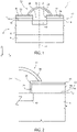
Figure 1 shows an integratedelectronic device 1, which includes amain body 2 delimited at top by a front surface Stop. Themain body 2 comprises asemiconductive substrate 4 and atop region 6, which may include a number of dielectric layers (not shown) and a number of metallization layers (not shown); in addition, thetop region 6 is delimited at top by the front surface Stop. - The integrated
electronic device 1 further includes a topconductive region 10, formed, as an example, by copper; the topconductive region 10 extends within thetop region 6, starting from the front surface Stop. Though not shown, in top view the topconductive region 10 may have a circular shape; in addition, the topconductive region 10 may belong to the so-called top metallization level of the integratedelectronic device 1. In a per se known manner, the topconductive region 10 is in electric contact with the electronic component formed within the integratedelectronic device 1. - In addition, the integrated
electronic device 1 includes apassivation structure 12, which includes, as an example, a firstdielectric region 14, which is made of silicon nitride and is arranged on the front surface Stop, in direct contact with thetop region 6 and with a peripheral portion of the topconductive region 10. - The
passivation structure 12 further includes a seconddielectric region 16, which is made of TEOS oxide and is arranged on the firstdielectric region 14, in direct contact. In addition, thepassivation structure 12 further includes a thirddielectric region 18, which is made of silicon nitride and is arranged on the seconddielectric region 16, in direct contact. - An
aperture 20 extends through the first, second and thirddielectric regions aperture 20 may have a circular shape. Theaperture 20 is delimited at bottom by an inner portion of the topconductive region 10; furthermore, theaperture 20 is laterally delimited by aside wall 21, which, to a first approximation, has a cylindrical shape and is formed by portions of the first, second and thirddielectric regions - The integrated
electronic device 1 further includes acontact structure 22, which in turn includes a first and a secondconductive contact region - In detail, the first
conductive contact region 24 is made of nickel. The firstconductive contact region 24 includes a lower portion, which extends within theaperture 20, in direct contact with the underlying inner portion of the topconductive region 10 and with theside wall 21, and an upper portion, which extends outside theaperture 20, above the abovementioned lower portion and on a portion of the thirddielectric region 18 that surrounds the upper part of theaperture 20. By adopting an orthogonal reference system XYZ such that the plane XY is parallel to the front surface Stop, to a first approximation the thickness (parallel to the Z axis) of the upper portion of the firstconductive contact region 24 decreases as the radial distance from an axis H (parallel to Z axis) increases. To a first approximation, the axis H is a symmetry axis of the firstconductive contact region 24, which has a mushroom-like shape. - The second
conductive contact region 26 is made of palladium and extends on the firstconducive contact region 24, in direct contact and approximately with a constant thickness, i.e. in a conformal manner. In particular, an inner portion of the secondconductive contact region 26 extends on the firstconductive contact region 24; an outer portion of the secondconductive contact region 26 extends on a portion of the thirddielectric region 18. - Though not shown, the second
conductive contact region 26 is connected to the external world, as an example through a wire bonding, i.e. by welding a conductive wire (not shown) to the secondconductive contact region 26. - From a practical point of view, the
contact structure 22 and the topconductive region 10 form a so-called pad, which allows to set an electric contact between the integratedelectronic device 1 and the external world. However, such a pad may by prone to the phenomenon of the corrosion of the topconductive region 10, for the following reasons. - The abovementioned first and second
conductive contact regions contact structure 22 are formed by means of electroless deposition; such a technique allows to form conductive regions on top of an underlying pre-existing conductive support and causes the contact structure to have the abovementioned mushroom-like shape. However, as shown inFigure 2 , it may happen that a crevice ("fenditura") 25 occurs between thecontact structure 22 and thepassivation structure 12. In particular, thecrevice 25 may extend between the lower portion of the firstconductive contact region 24 and theside wall 21, as well as between the upper portion of the firstconductive contact region 24 and the abovementioned portion of the thirddielectric region 18 surrounding the upper part of theaperture 20; in addition, thecrevice 25 may extend between the secondconductive contact region 26 and an underlying portion of the thirddielectric region 18. - The
crevice 25 is delimited at bottom by an exposed portion of the topconductive region 10; therefore, thecrevice 25 forms a path through which contaminants (as an example, made of metals or halogens such as chlorine and fluorine) can come into contact with the topconductive region 10, thereby causing an unwanted corrosion of this latter, and thus damaging the pad. - The aim of the present invention is consequently to provide a pad structure for an integrated electronic device, that will enable the drawbacks of the prior art to be overcome at least in part.
- According to the present invention, an integrated electronic device and a corresponding manufacturing process are provided, as defined in the annexed claims.
- For a better understanding of the present invention, preferred embodiments thereof are now described, purely by way of non-limiting example, with reference to the attached drawings, wherein:
-
Figure 1 is a schematic cross-sectional view (not in scale) of a portion of an integrated electronic device; -
Figure 2 is a schematic cross-sectional view (not in scale) of a portion of an integrated electronic device subjected to a crevice; -
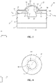
Figure 3 is a schematic cross-sectional view (not in scale) of the present integrated electronic device; -
Figure 4 is a schematic top plan view of a portion of the integrated electronic device shown inFigure 3 ; -
Figures 5-10 are schematic cross-sectional views (not in scale) of portions of an integrated electronic device, in successive manufacturing steps; and -
Figure 11 is a schematic cross-sectional view (not in scale) of a variant of the present integrated electronic device. -
Figure 3 shows an integratedelectronic device 31, which will be described here below with reference to the differences with respect to the integratedelectronic device 1 shown inFigure 1 . Elements already present in the integratedelectronic device 1 shown inFigure 1 will have the same reference signs, unless otherwise stated. - In detail, the integrated
electronic device 31 includes abarrier structure 35, which includes afirst barrier region 37. Furthermore, thefirst barrier region 37 is made of a material that prevents the migration/diffusion of contaminants (such as metals or halogens); as an example, thefirst barrier region 37 may be made of tungsten-titanium. - In greater detail, the
first barrier region 37 is arranged on the firstdielectric region 14, in direct contact. As an example, as shown inFigure 4 , in top view thefirst barrier region 37 has the shape of an annulus. - In addition, the
first barrier region 37 and the firstdielectric region 14 form the side wall (here designated by 51) of the aperture (here designated by 50), to which in the following reference will be made as thefirst aperture 50. Furthermore, in the following reference will be made to theside wall 51 as thefirst side wall 51. - In practice, the
first aperture 50 extends through the firstdielectric layer 14 and thefirst barrier region 37; furthermore, thefirst aperture 50 has a cylindrical shape. - The second dielectric region (here designated by 56) extends on the
first barrier region 37, in direct contact, as well as on portions of the firstdielectric region 14 laterally offset with respect to thefirst barrier region 37. The third dielectric region (here designated by 58) extends on the seconddielectric region 56, in direct contact. - A
second aperture 60 extends through the second and the thirddielectric region first aperture 50. Thesecond aperture 60 may have a cylindrical shape, vertically aligned with the underlyingfirst aperture 50 and with a circular base greater than the circular base of thefirst aperture 50, so that a peripheral portion of thesecond aperture 60 is delimited at bottom by a portion of thefirst barrier region 37 that surrounds thefirst aperture 50, and an inner portion of thesecond aperture 60 overlies thefirst aperture 50. Thesecond aperture 60 is laterally delimited by a corresponding side wall designated by 61, to which reference will be made as thesecond side wall 61; thesecond side wall 61 is formed by the second and the thirddielectric region - The lower portion of first
conductive contact region 24 extends within the first and thesecond aperture conductive contact region 24 extends outside thesecond aperture 60, above the abovementioned lower portion and on a portion of the thirddielectric region 58 that surrounds the upper part of thesecond aperture 60, with a thickness (parallel to the Z axis) that, to a first approximation, decreases as the radial distance from the axis H increases. The secondconductive contact region 26 still extends on the firstconductive contact region 24, in direct contact. - In greater detail, the lower portion of first
conductive contact region 24 contacts either the abovementioned portion of thefirst barrier region 37 that delimits the peripheral portion of thesecond aperture 60 at bottom and the portion of thefirst side wall 51 formed by thefirst barrier region 37, with which it forms a strong bond, little prone to the phenomenon of crevice. - In practice, even if in use a crevice may occur between the
second side wall 61 and the lower portion of firstconductive contact region 24, such a crevice is closed at bottom by thebarrier structure 35, because of the strong bond present between the firstconductive contact region 24 and thefirst barrier region 37. Since thefirst barrier region 37 acts as a stopper region for the contaminants, these latter cannot come into contact with the topconductive region 10, which is thus protected from corrosion. - The integrated
electronic device 31 can be manufactured through the manufacturing process described here below. - In detail, after forming in a per se known manner the
main body 2 and the topconductive region 10, a firstdielectric layer 114 of silicon nitride is formed on the front surface Stop, as shown inFigure 5 ; in addition, aconductive layer 137 is formed, on top of the firstdielectric layer 114, as an example by physical vapor deposition (PVD). Theconductive layer 137 is made of tungsten-titanium. In addition, thedielectric layer 114 acts as a "capping layer", which prevents the corrosion of the underlying topconductive region 10. - As shown in
Figure 6 , portions of theconductive layer 137 are then selectively removed, as an example by means of dry or wet etch, so that the remaining portion of theconductive layer 137 forms thefirst barrier region 37, and thus thebarrier structure 35. - In particular, the
first barrier region 37 laterally delimits awindow 140, delimited at bottom by the firstdielectric layer 114 and overlying, at a distance, the topconductive region 10; in addition, thefirst barrier region 37 leaves exposed portions of the firstdielectric layer 114 that are laterally offset with respect to thefirst barrier region 37. - Afterwards, as shown in
Figure 7 , a seconddielectric layer 156 of TEOS oxide is formed on the exposed portions of the firstdielectric layer 114, on thefirst barrier region 37 and within thewindow 140; in addition, a thirddielectric layer 158 of silicon nitride is formed on the seconddielectric layer 156. - Afterwards, as shown in
Figure 8 , a portion of the thirddielectric layer 158 and an underlying portion of the seconddielectric layer 156 are selectively removed, as an example by means of a dry etch, which is performed through amask 159 arranged on the thirddielectric layer 158. In such a way, thesecond aperture 60 is formed, through the second and the thirddielectric layer dielectric layer 156 that extends within thewindow 140 is removed, so that the portion of the firstdielectric layer 114 that delimits thewindow 140 at bottom is exposed. In addition, this etch cause the exposure of a portion of thebarrier region 37 that delimits thesecond aperture 60 at bottom and laterally delimits thewindow 140. The remaining portions of the second and the thirddielectric layer dielectric region - Afterwards, as shown in
Figure 9 , by keeping in place themask 159, a further selective etch is performed, so as to selectively remove the portion of thefirst dielectric layer 114 arranged under thewindow 140, thereby exposing the inner portion of the topconductive region 10 and forming thefirst aperture 50. The remaining portion of thefirst dielectric layer 114 forms the firstdielectric region 14. - From a practical point of view, this etch, which is based on a chemistry different from the one of the etch shown in
Figure 8 , is guided by thefirst barrier region 37, along with themask 159. - Afterwards, as shown in
Figure 10 , themask 159 is removed and the firstconductive contact region 24 is formed by electroless deposition, starting from the exposed inner portion of the topconductive region 10 and from the exposed portion of thebarrier region 37. - Afterwards, although not shown, the second
conductive contact region 26 is formed by electroless deposition, on the firstconductive contact region 24. - The manufacturing process of the integrated
electronic device 31 may then continue in a per se known manner, as an example by forming a further protection region (not shown). - The advantages of the present solution emerge clearly from the foregoing description. In this connection, it should again be noted how, according to the present solution, the top
conductive region 10 is protected from corrosion, because thebarrier structure 35 acts as a stopper structure that is tightly bonded to the firstconductive contact region 24, thereby leading to an improved pad structure. - Finally, it is clear that modifications and variations may be made to what has been described and illustrated herein, without thereby departing from the scope of the present invention, as defined in the annexed claims.
- In general, the materials may be different from the previously cited ones.
- The passivation structure may be formed by a different number of dielectric regions (as an example, only one region or more than two regions). As an example, the third
dielectric region 58 may be absent. - Similarly, the
first barrier region 37 may have a different shape; as an example, in top view, thefirst barrier region 37 may have the shape of a polygonal frame ("cornice"). In addition, thefirst barrier region 37 may be formed by a conductive material different from tungsten-titanium. - Furthermore, the
barrier structure 35 may be formed by a stack of two or more barrier regions made of conductive materials that prevent the migration/diffusion of the contaminants. As an example, thebarrier structure 35 may be formed by one of the following barrier region stacks: TaNTa (two barrier regions), TiN (one barrier region), TiTiN (two barrier regions) or TiTiNTi (three barrier regions). In this case, thefirst aperture 50 extends through the stack of barrier regions. - As an example,
Figure 11 shows an example in which thebarrier structure 35 includes asecond barrier region 39, which is arranged on thefirst barrier region 37, in direct contact. In top view, thesecond barrier region 39 may have the same shape as the underlyingfirst barrier region 37; thefirst aperture 50 extends through the first and thesecond barrier region second barrier region second barrier region first side wall 51. In this case, the peripheral portion of thesecond aperture 60 is delimited at bottom by a portion of thesecond barrier region 39; the lower portion of firstconductive contact region 24 contacts either the portion of thebarrier region 39 that delimits the peripheral portion of thesecond aperture 60 at bottom and the portions of thefirst side wall 51 formed by the first and thesecond barrier region - The first and the second
conductive contact region conductive contact region 26 may be absent, in which case the wire bonding is welded on the firstconductive contact region 24; as an alternative, one or more additional conductive contact regions may be formed on the secondconductive contact region 26. As an example, thecontact structure 22 may be formed by the stack NiPdAu, i.e. by three conductive contact regions. - The shapes of the first and the
second aperture second side wall - The top
conductive region 10 may be made of a material different from copper. In addition, the topconductive region 10 may have a different shape; as an example, in top view, the topconductive region 10 may have a polygonal shape. - The inner portion of the top
conductive region 10, which delimits thefirst aperture 50 at bottom, may be slightly overetched with respect to the peripheral portion of the topconductive region 10, which lies under the firstdielectric region 14.
Claims (11)
- An integrated electronic device including:- a main body (2) delimited by a front surface (Stop);- a top conductive region (10) extending within the main body (2), starting from the front surface (Stop);- a first dielectric region (14) extending on the front surface (Stop); and- a barrier structure (35), arranged on the first dielectric region (14);and wherein a first aperture (50) extends through the barrier structure (35) and the first dielectric region (14), said first aperture (50) being delimited at bottom by the top conductive region (10); said integrated electronic device (31) further comprising a contact structure (22) including at least a first conductive region (24) extending within the first aperture (50), in direct contact with the top conductive region (10) and the barrier structure (35).
- The integrated electronic device according to claim 1, wherein the barrier structure (35) includes a stack of one or more barrier regions (37,39) made of one or more conductive materials suitable for preventing the diffusion of metal and halogen contaminants through the barrier structure (35).
- The integrated electronic device according to claim 2, wherein said one or more barrier regions (37,39) are made of conductive materials different from the materials of the top conductive region (10) and of the first conductive region (24) .
- The integrated electronic device according to any of the preceding claims, further comprising a second dielectric region (56,58) extending on the barrier structure (35); and wherein a second aperture (60) extends through the second dielectric region (56,58), said second aperture (60) having a respective inner portion, which communicates with the underlying first aperture (50), and a respective peripheral portion, which is delimited at bottom by a portion of the barrier structure (35); and wherein the first conductive region (24) extends also within the second aperture (60), on said portion of the barrier structure (35).
- The integrated electronic device according to claim 4, wherein the first conductive region (24) extends also above the second aperture (60) and has a mushroom-like shape.
- The integrated electronic device according to any of the preceding claims, wherein the contact structure (22) further comprises a second conductive region (26) extending on the first conductive region (24), the first and the second conductive region (24,26) being respectively made of nickel and palladium.
- A process for manufacturing an integrated electronic device, comprising:- forming a main body (2) delimited by a front surface (Stop);- forming a top conductive region (10) extending within the main body (2), starting from the front surface (Stop);- forming a first dielectric region (14) on the front surface (Stop); and- forming a barrier structure (35) on the first dielectric region (14);- forming a first aperture (50) through the barrier structure (35) and the first dielectric region (14), said first aperture (50) being delimited at bottom by the top conductive region (10); and- forming a contact structure (22) including at least a first conductive region (24) extending within the first aperture (50), in direct contact with the top conductive region (10) and the barrier structure (35).
- The manufacturing process according to claim 7, further comprising forming a first dielectric layer (114) on the front surface (Stop) and forming said barrier structure (35) on the first dielectric layer (114), so that the barrier structure (35) laterally delimits a window (140) closed at bottom by the first dielectric layer (114); said manufacturing process further including:- forming at least a second dielectric layer (156) extending on the barrier structure (35) and within the window (140) ;- through a temporary mask (159), selectively removing portions of said second dielectric layer (156) that extend on the barrier structure (35) and within the window (140), so as to form a second aperture (60) extending through the second dielectric layer (156), said second aperture (60) having a respective inner portion, which communicates with the underlying window (140), and a respective peripheral portion, which is delimited at bottom by a portion of the barrier structure (35); and then- through said temporary mask (159), selectively removing the portion of the first dielectric layer (114) that closes the window (140) at bottom, so as to form said first aperture (50).
- The manufacturing process according to claims 7 or 8, comprising forming said first conductive region (24) by electroless deposition.
- The manufacturing process according to claim 9, further comprising forming, by electroless deposition, a second conductive region (26) on the first conductive region (24).
- The manufacturing process according to any of claims 7-10, wherein the barrier structure (35) includes a stack of one or more barrier regions (37,39) made of one or more conductive materials suitable for preventing the diffusion of metal and halogen contaminants through the barrier structure (35).
Applications Claiming Priority (1)
| Application Number | Priority Date | Filing Date | Title |
|---|---|---|---|
| IT102021000017021A IT202100017021A1 (en) | 2021-06-29 | 2021-06-29 | ELECTRONIC DEVICE INTEGRATED WITH A PITCH STRUCTURE INCLUDING A BARRIER STRUCTURE AND RELATED MANUFACTURING PROCESS |
Publications (2)
| Publication Number | Publication Date |
|---|---|
| EP4113598A2 true EP4113598A2 (en) | 2023-01-04 |
| EP4113598A3 EP4113598A3 (en) | 2023-05-24 |
Family
ID=77802111
Family Applications (1)
| Application Number | Title | Priority Date | Filing Date |
|---|---|---|---|
| EP22181496.5A Withdrawn EP4113598A3 (en) | 2021-06-29 | 2022-06-28 | Integrated electronic device with a pad structure including a barrier structure and related manufacturing process |
Country Status (3)
| Country | Link |
|---|---|
| US (1) | US20220415705A1 (en) |
| EP (1) | EP4113598A3 (en) |
| IT (1) | IT202100017021A1 (en) |
Families Citing this family (1)
| Publication number | Priority date | Publication date | Assignee | Title |
|---|---|---|---|---|
| US12557686B2 (en) | 2022-11-11 | 2026-02-17 | Stmicroelectronics S.R.L. | Semiconductor package or device with barrier layer |
Family Cites Families (13)
| Publication number | Priority date | Publication date | Assignee | Title |
|---|---|---|---|---|
| US20020019127A1 (en) * | 1997-02-14 | 2002-02-14 | Micron Technology, Inc. | Interconnect structure and method of making |
| US6448657B1 (en) * | 1999-04-21 | 2002-09-10 | Applied Materials, Inc. | Structure for reducing junction spiking through a wall surface of an overetched contact via |
| US7504652B2 (en) * | 2005-07-13 | 2009-03-17 | Taiwan Semiconductor Manufacturing Company, Ltd. | Phase change random access memory |
| US8129267B2 (en) * | 2008-03-21 | 2012-03-06 | International Business Machines Corporation | Alpha particle blocking wire structure and method fabricating same |
| US9064875B2 (en) * | 2010-09-29 | 2015-06-23 | Infineon Technologies Ag | Semiconductor structure and method for making same |
| US9443772B2 (en) * | 2014-03-19 | 2016-09-13 | Globalfoundries Inc. | Diffusion-controlled semiconductor contact creation |
| JP2017069381A (en) * | 2015-09-30 | 2017-04-06 | ルネサスエレクトロニクス株式会社 | Semiconductor device and manufacturing method of semiconductor device |
| US10176999B2 (en) * | 2015-12-31 | 2019-01-08 | Taiwan Semiconductor Manufacturing Company Ltd. | Semiconductor device having a multi-layer, metal-containing film |
| US10796954B2 (en) * | 2018-06-28 | 2020-10-06 | Taiwan Semiconductor Manufacturing Company Ltd. | Semiconductor structure and method for forming the same |
| US10804230B2 (en) * | 2018-10-17 | 2020-10-13 | Taiwan Semiconductor Manufacturing Company Ltd. | Semiconductor package and method of manufacturing the same |
| TWI714093B (en) * | 2019-05-21 | 2020-12-21 | 友達光電股份有限公司 | Array substrate |
| US10867892B1 (en) * | 2019-08-22 | 2020-12-15 | Taiwan Semiconductor Manufacturing Company Ltd. | Semiconductor structure and manufacturing method thereof |
| US11973050B2 (en) * | 2021-02-02 | 2024-04-30 | Taiwan Semiconductor Manufacturing Company, Ltd. | Method for forming an upper conductive structure having multilayer stack to decrease fabrication costs and increase performance |
-
2021
- 2021-06-29 IT IT102021000017021A patent/IT202100017021A1/en unknown
-
2022
- 2022-06-23 US US17/848,050 patent/US20220415705A1/en active Pending
- 2022-06-28 EP EP22181496.5A patent/EP4113598A3/en not_active Withdrawn
Also Published As
| Publication number | Publication date |
|---|---|
| EP4113598A3 (en) | 2023-05-24 |
| IT202100017021A1 (en) | 2022-12-29 |
| US20220415705A1 (en) | 2022-12-29 |
Similar Documents
| Publication | Publication Date | Title |
|---|---|---|
| JP5455285B2 (en) | Solder bump structure for flip chip semiconductor device and manufacturing method thereof | |
| US5707894A (en) | Bonding pad structure and method thereof | |
| US10580726B2 (en) | Semiconductor devices and semiconductor packages including the same, and methods of manufacturing the semiconductor devices | |
| US7544538B2 (en) | Method of forming semiconductor chips, the semiconductor chips so formed and chip-stack package having the same | |
| US12249586B2 (en) | Film structure for bond pad | |
| KR101163974B1 (en) | Routing under bond pad for the replacement of an interconnect layer | |
| US20070052067A1 (en) | Semiconductor device, method of manufacturing the same, circuit board, and method of manufacturing the same | |
| US20080136038A1 (en) | Integrated circuits with conductive features in through holes passing through other conductive features and through a semiconductor substrate | |
| US9893036B2 (en) | Semiconductor device and manufacturing method of semiconductor device | |
| US8927411B2 (en) | System and method for forming an aluminum fuse for compatibility with copper BEOL interconnect scheme | |
| US6768199B2 (en) | Flip chip type semiconductor device and method of fabricating the same | |
| US11244915B2 (en) | Bond pads of semiconductor devices | |
| US8035215B2 (en) | Semiconductor device and manufacturing method of the same | |
| TWI762800B (en) | Semiconductor device and fabrication method for the same | |
| US20220415705A1 (en) | Integrated electronic device with a pad structure including a barrier structure and related manufacturing process | |
| CN210640232U (en) | a semiconductor structure | |
| US9768132B2 (en) | Semiconductor structure and method of forming the same | |
| JP2011108690A (en) | Semiconductor device and method for manufacturing the same | |
| CN112885803A (en) | Semiconductor structure and manufacturing method thereof | |
| US10535576B2 (en) | Semiconductor devices and methods of formation thereof | |
| JP3897339B2 (en) | Structure and method for minimizing plasma charging damage of SOI devices | |
| CN100530577C (en) | Semiconductor device and method of manufacturing the same | |
| TWI808207B (en) | Semiconductor device | |
| JP6963396B2 (en) | Manufacturing method of electronic parts | |
| JP2000286383A (en) | Semiconductor device and manufacturing method thereof |
Legal Events
| Date | Code | Title | Description |
|---|---|---|---|
| PUAI | Public reference made under article 153(3) epc to a published international application that has entered the european phase |
Free format text: ORIGINAL CODE: 0009012 |
|
| STAA | Information on the status of an ep patent application or granted ep patent |
Free format text: STATUS: THE APPLICATION HAS BEEN PUBLISHED |
|
| AK | Designated contracting states |
Kind code of ref document: A2 Designated state(s): AL AT BE BG CH CY CZ DE DK EE ES FI FR GB GR HR HU IE IS IT LI LT LU LV MC MK MT NL NO PL PT RO RS SE SI SK SM TR |
|
| PUAL | Search report despatched |
Free format text: ORIGINAL CODE: 0009013 |
|
| AK | Designated contracting states |
Kind code of ref document: A3 Designated state(s): AL AT BE BG CH CY CZ DE DK EE ES FI FR GB GR HR HU IE IS IT LI LT LU LV MC MK MT NL NO PL PT RO RS SE SI SK SM TR |
|
| RIC1 | Information provided on ipc code assigned before grant |
Ipc: H01L 21/60 20060101ALN20230420BHEP Ipc: H01L 23/31 20060101ALI20230420BHEP Ipc: H01L 23/00 20060101ALI20230420BHEP Ipc: H01L 23/485 20060101AFI20230420BHEP |
|
| STAA | Information on the status of an ep patent application or granted ep patent |
Free format text: STATUS: REQUEST FOR EXAMINATION WAS MADE |
|
| 17P | Request for examination filed |
Effective date: 20231121 |
|
| RBV | Designated contracting states (corrected) |
Designated state(s): AL AT BE BG CH CY CZ DE DK EE ES FI FR GB GR HR HU IE IS IT LI LT LU LV MC MK MT NL NO PL PT RO RS SE SI SK SM TR |
|
| STAA | Information on the status of an ep patent application or granted ep patent |
Free format text: STATUS: EXAMINATION IS IN PROGRESS |
|
| 17Q | First examination report despatched |
Effective date: 20250319 |
|
| STAA | Information on the status of an ep patent application or granted ep patent |
Free format text: STATUS: THE APPLICATION HAS BEEN WITHDRAWN |
|
| 18W | Application withdrawn |
Effective date: 20250509 |