EP4111177B1 - Verfahren zur bestimmung einer materialeigenschaft eines festen substrats - Google Patents
Verfahren zur bestimmung einer materialeigenschaft eines festen substrats Download PDFInfo
- Publication number
- EP4111177B1 EP4111177B1 EP20707617.5A EP20707617A EP4111177B1 EP 4111177 B1 EP4111177 B1 EP 4111177B1 EP 20707617 A EP20707617 A EP 20707617A EP 4111177 B1 EP4111177 B1 EP 4111177B1
- Authority
- EP
- European Patent Office
- Prior art keywords
- substrate
- array
- determining
- plasmonic nanostructures
- material property
- Prior art date
- Legal status (The legal status is an assumption and is not a legal conclusion. Google has not performed a legal analysis and makes no representation as to the accuracy of the status listed.)
- Active
Links
Images


Classifications
-
- G—PHYSICS
- G01—MEASURING; TESTING
- G01N—INVESTIGATING OR ANALYSING MATERIALS BY DETERMINING THEIR CHEMICAL OR PHYSICAL PROPERTIES
- G01N21/00—Investigating or analysing materials by the use of optical means, i.e. using sub-millimetre waves, infrared, visible or ultraviolet light
- G01N21/17—Systems in which incident light is modified in accordance with the properties of the material investigated
- G01N21/55—Specular reflectivity
- G01N21/552—Attenuated total reflection
- G01N21/553—Attenuated total reflection and using surface plasmons
- G01N21/554—Attenuated total reflection and using surface plasmons detecting the surface plasmon resonance of nanostructured metals, e.g. localised surface plasmon resonance
-
- G—PHYSICS
- G01—MEASURING; TESTING
- G01N—INVESTIGATING OR ANALYSING MATERIALS BY DETERMINING THEIR CHEMICAL OR PHYSICAL PROPERTIES
- G01N21/00—Investigating or analysing materials by the use of optical means, i.e. using sub-millimetre waves, infrared, visible or ultraviolet light
- G01N21/84—Systems specially adapted for particular applications
- G01N21/8422—Investigating thin films, e.g. matrix isolation method
Definitions
- the invention relates to a device/method for determining a material property of a solid substrate.
- the invention further relates to the use of an array of plasmonic nanoparticles provided on a solid substrate for determining a material property of the solid substrate.
- Localized surface plasmons also referred to as nanoplasmons
- nanoplasmons are collective electron oscillations that couple to electromagnetic radiation and thereby localize and enhance the electromagnetic field on a nanoscale.
- Plasmonic nanostructures may be understood as nanoplasmonic optical antennas which are able to interact with visible light similarly to how regular radio or mobile phone antennas operate, i.e., by capturing the propagating radiation and transforming it into local current at resonance frequencies. With such nanoplasmonic optical antennas, very high electromagnetic field concentrations become available that can be explored for sensing applications.
- Nanoplasmonic sensing is widely explored in applications, and several commercial solutions exist for detecting various gases and/or biological species, such as proteins, by means of such sensing.
- KR 2010 0082820 A relates to an optical apparatus with a plasmonic device which generates a near field having a variable strength according to properties of an object-under-test, in front of a nano-aperture of a thin metal film.
- a plasmonic nanostructure is to be interpreted as a metallic and/or semiconductor component, particle or structure having a size and shape allowing for the exploitation of localized surface plasmon resonances.
- the size of such a plasmonic nanostructure may be such that the nanostructure has an equivalent spherical diameter of 1 nm-10 ⁇ m, depending on the shape and material of the nanostructure, wherein larger sizes within this range are generally applicable to doped semiconductor components.
- An object of the invention is to provide a method for determining a material property of a solid substrate, which method is in at least some aspect improved with respect to prior art methods.
- plasmonic nanostructures provided on a surface of a solid substrate may be used not only for determining properties of e.g. a solid, gaseous or liquid medium surrounding nanostructures provided on the solid substrate, but also for determining material properties of the solid substrate itself, which material properties are related to a refractive index of the material. This enables quick and accurate determination of material properties related to the refractive index of the solid substrate, such as atomic compositions of thin films and similar.
- the proposed method could be used for sensing with high sensitivity the compositions of various multi-component functional thin films, including for example magnetic tricomponent systems, like GdFeCo, in which the composition defines the ability of such systems to be switched in their magnetization state or remagnetized by ultra-short (femtosecond) light pulses, or steel carbide thin films in which the composition defines stress in the thin film and its eventual hardness.
- magnetic tricomponent systems like GdFeCo
- the composition defines the ability of such systems to be switched in their magnetization state or remagnetized by ultra-short (femtosecond) light pulses
- steel carbide thin films in which the composition defines stress in the thin film and its eventual hardness.
- the optical extinction peak is generally determined in the case of a transparent solid substrate, while as the reflectance peak is used in the case of an opaque or reflective solid substrate, or in case of a semi-transparent solid substrate.
- Such techniques include top-down techniques such as lithographic techniques, for example electron beam lithography, focused ion-beam lithography, (nano)imprint lithography and photolithography, and bottom-up techniques relying on self-assembly of nanostructures.
- illuminating the at least one portion of the substrate comprises illuminating the at least one portion of the substrate with light from a spectral range including visible light and/or near-infrared light, and/or with single-wavelength or essentially single-wavelength light.
- the light may preferably comprise white light.
- light from a flash light, a mobile phone flash, or another light source may be used.
- essentially single wavelength is herein to be understood single wavelength light with a given spectral broadening.
- Light source providing such light include lasers, such as portable laser pointers / laser diodes.
- determining the optical extinction and/or reflectance peak of the illuminated array of plasmonic nanostructures comprises detecting a spectrum comprising at least light reflected off and/or light scattered off the illuminated array.
- optical extinction may be measured, including scattering and absorption, while as otherwise reflectance may be measured.
- the material property is a chemical composition and/or an atomic composition of the at least one portion of the substrate.
- determining the material property comprises determining the chemical composition and/or the atomic composition of the at least one portion of the substrate.
- the chemical / atomic composition affects the refractive index of the at least one portion of the substrate and thereby also affects the optical extinction and/or reflectance peak of the illuminated array of plasmonic nanostructures provided on the substrate.
- the at least one portion of the substrate comprises a metallic material.
- the material property may be a material property of the metallic material.
- the metallic material is a magnetic metal alloy comprising at least one element selected from the group of Fe, Co and Ni.
- Such metal alloys may be used in e.g. ferromagnetic or ferrimagnetic or antiferromagnetic thin films used in all-optical ultrafast magnetization switching applications.
- the metallic material is in the form of a thin film.
- the thin film comprises at least one metallic layer, but may comprise more than one metallic layer, such as two or more metallic layers, in which case the method may be used for determining the material property of at least one metallic layer of the thin film, such as of a metallic layer at a depth of 20 nm or less from a surface of the solid substrate.
- the at least one portion of the substrate herein comprises the thin film, or at least one layer of the thin film.
- the thin film is a terbium-cobalt thin film having an atomic composition Tb x Co 100-x , wherein determining the material property comprises determining the number x.
- the material property is thus the atomic composition of the thin film.
- the thin film is a gadolinium-iron-cobalt thin film having an atomic composition Gd x Fe y Co z , wherein determining the material property comprises determining at least one of the numbers x, y and z.
- the material property is thus the atomic composition of the thin film.
- the at least one portion of the substrate comprises a titanium carbide (TiC) or tungsten carbide (WC) material thin film.
- TiC titanium carbide
- WC tungsten carbide
- the material property may be a chemical, microstructural or physical property affecting the refractive index of the TiC or WC material affecting its hardness.
- the material property which is determined may be a slight deviation in C, Ti and/or W concentrations from 50%.
- the method further comprises:
- the nanostructures are protected by the dielectric coating. It is also possible to provide a first thin dielectric coating layer between the substrate and the array of plasmonic nanostructures, and a second thin dielectric coating layer atop the plasmonic nanostructures, the plasmonic nanostructures thus being embedded in the dielectric coating.
- the plasmonic nanostructures have a mean equivalent diameter of 10-500 nm, or 20-400 nm, or 30-200 nm, as measured in a plane parallel with a surface on which the plasmonic nanostructures are provided.
- the mean equivalent diameter may for example be understood as a mean equivalent spherical diameter.
- the size may e.g. be determined using image analysis of scanning and/or transmission electron microscopy images, or by atomic force microscopy and/or profilometry images. Larger nanostructures can be identified by the high-resolution optical microscopy (confocal, high magnification, with digital zoom).
- providing the array of plasmonic nanostructures comprises using nanoimprint lithography.
- Nanoimprint lithography may be used to provide an ordered or a disordered array of nanostructures depending on a template used in the nanoimprint process.
- the nanostructures may alternatively be transferred from another substrate onto the solid substrate.
- providing the array of plasmonic nanostructures comprises using a colloidal lithography based fabrication method to provide a short-range ordered array of plasmonic nanostructures.
- This is a relatively fast and efficient way of providing a short-range ordered array of plasmonic nanostructures lacking long-range order, thereby eliminating long-range optical coupling effects such as optical diffraction, Wood anomalies and similar.
- determining the material property comprises comparing the detected optical extinction and/or reflectance peak to stored data describing said optical extinction and/or reflectance peak as a function of the material property.
- the stored data may be in the form of tabulated values.
- a solid substrate 1 on which an array 2 of plasmonic nanostructures 3 is provided is shown in figs. 1-2 .
- the solid substrate 2 may for example be a silicon wafer 4 or similar, having a functional thin film 5 grown on its top surface.
- the array 2 of plasmonic nanostructures 3 is provided on a surface portion of the solid substrate 1.
- a thin protective coating 6 is provided between the thin film 5 and the array 2 of plasmonic nanostructures 3.
- the plasmonic nanostructures 3 are in the form of metal nanostructures, such as metal disks or metal cylinders having a height h and a diameter d.
- the portion of the solid substrate 1 on which the array 2 is provided is herein a relatively small surface portion of the substrate 1.
- a centre-to-centre spacing D between neighbouring nanostructures 3 is shown to be irregular in figs. 1-2 , but the nanostructures may alternatively be arranged according to an ordered pattern at regular distances from each other.
- a method for determining a material property of the solid substrate according to an embodiment of the invention is illustrated in the flow chart of fig. 3 .
- the method comprises - inter alia and as further defined with claim 1 - the following steps:
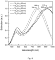
- arrays of plasmonic Ag nanorings 3 were provided on top of the TbCo thin films 5 and the Al 2 O 3 coating 6, the nanorings 3 being arranged with a central axis C extending perpendicularly to a surface of the substrate 1.
- the ferrimagnetic Tb x Co 100-x thin films 5 were deposited on standard SiO 2 plates 4.
- the nanorings 3 were fabricated using a hole-mask colloidal lithography technique in accordance with a method described in a previously published article by H. Fredriksson et al., Hole-mask lithography, Adv. Mater., 19, 4297 (2007 ).
- the nanorings 3 were concentric, i.e. centrosymmetric, with a geometry determined by material deposition process parameters used during the fabrication.
- the nanorings 3 exhibited an outer diameter d2 of 110 nm and an inner diameter d1 of 35 nm.
- the atomic concentrations of Tb in the ferrimagnetic thin films 5 were determined to be in the range of 24-29 % as listed in table I.
- the accuracy of the method is well comparable to standard ion beam nuclear analytical methods of Rutherford backscattering spectrometry (RBS) and particle-induced x-ray emission (PIXE).
- Table I Film thickness (nm) Resonance peak (nm) Atomic composition 20 760 Tb 29 Co 71 40 800 Tb 29 Co 71 20 900 Tb 26 Co 74 30 915 Tb 26 Co 74 40 925 Tb 24 Co 76
Landscapes
- Chemical & Material Sciences (AREA)
- Physics & Mathematics (AREA)
- Biochemistry (AREA)
- Life Sciences & Earth Sciences (AREA)
- Health & Medical Sciences (AREA)
- Analytical Chemistry (AREA)
- General Health & Medical Sciences (AREA)
- General Physics & Mathematics (AREA)
- Immunology (AREA)
- Pathology (AREA)
- Mathematical Physics (AREA)
- Engineering & Computer Science (AREA)
- Nanotechnology (AREA)
- Investigating Or Analysing Materials By Optical Means (AREA)
Claims (15)
- Verfahren zum Bestimmen einer Materialeigenschaft eines festen Substrats (1), das Verfahren umfassend:- Bereitstellen (S1) eines Arrays (2) von plasmonischen Nanostrukturen (3) auf mindestens einem Abschnitt des Substrats (1),- Beleuchten (S2) des mindestens einen Abschnitts des Substrats (1), auf dem das Array (2) von plasmonischen Nanostrukturen (3) angeordnet ist,- Bestimmen (S3) einer optischen Extinktion und/oder Reflexionsspitze des beleuchteten Arrays (2) von plasmonischen Nanostrukturen (3), das auf dem Substrat (1) bereitgestellt ist,- basierend auf der bestimmten optischen Extinktion und/oder Reflexionsspitze, Bestimmen (S4) der Materialeigenschaft des mindestens einen Abschnitts des Substrats (1), wobei das Bestimmen der Materialeigenschaft das Bestimmen einer chemischen Zusammensetzung und/oder einer atomaren Zusammensetzung des mindestens einen Abschnitts des Substrats (1) durch Vergleichen der erfassten optischen Extinktion und/oder Reflexionsspitze mit gespeicherten Daten oder einer bekannten Beziehung umfasst, die die optische Extinktion und/oder Reflexionsspitze in Abhängigkeit von der Materialeigenschaft beschreibt.
- Verfahren nach Anspruch 1, wobei das Beleuchten des mindestens einen Abschnitts des Substrats (1) das Beleuchten des mindestens einen Abschnitts des Substrats (1) mit Licht aus einem Spektralbereich, der sichtbares Licht und/oder Nahinfrarotlicht einschließt, und/oder mit Einzelwellenlängen- oder im Wesentlichen Einzelwellenlängen-Licht umfasst.
- Verfahren nach Anspruch 1 oder 2, wobei das Bestimmen der optischen Extinktion und/oder Reflexionsspitze des beleuchteten Arrays (2) von plasmonischen Nanostrukturen (3) das Erfassen eines Spektrums umfasst, umfassend mindestens Licht, das von dem beleuchteten Array (2) reflektiert und/oder Licht, das von diesem gestreut wird.
- Verfahren nach einem der vorstehenden Ansprüche, wobei der mindestens eine Abschnitt des Substrats (1) ein metallisches Material umfasst.
- Verfahren nach Anspruch 4, wobei das metallische Material eine magnetische Metalllegierung ist, umfassend mindestens ein Element, das aus der Gruppe von Fe, Co und Ni ausgewählt ist.
- Verfahren nach Anspruch 4 oder 5, wobei das metallische Material in Form eines Dünnfilms (5) vorliegt.
- Verfahren nach Anspruch 6, wobei der Dünnfilm (5) ein Terbium-Kobalt-Dünnfilm ist, der eine atomare Zusammensetzung TbxCo100-x aufweist, wobei das Bestimmen der Materialeigenschaft das Bestimmen der Anzahl x umfasst, oder
wobei der Dünnfilm (5) ein Gadolinium-Eisen-Kobalt-Dünnfilm ist, der eine atomare Zusammensetzung GdxFeyCoz aufweist, und wobei das Bestimmen der Materialeigenschaft das Bestimmen mindestens einer der Zahlen x, y und z umfasst. - Verfahren nach einem der Ansprüche 1 bis 3, wobei der mindestens eine Abschnitt des Substrats (1) einen Titancarbid (TiC)- oder Wolframcarbid (WC)-Material-Dünnfilm umfasst.
- Verfahren nach einem der vorstehenden Ansprüche, ferner umfassend:- Bereitstellen einer dielektrischen Beschichtung (6) auf dem Substrat (1), wie einer dielektrischen Beschichtung (6), umfassend eine Alum iniumoxidbeschichtung,wobei das Array von plasmonischen Nanostrukturen auf einer Oberfläche der dielektrischen Beschichtung (6) bereitgestellt ist oder wobei das Array (2) von plasmonischen Nanostrukturen (3) zwischen dem Substrat (1) und der dielektrischen Beschichtung (6) bereitgestellt ist.
- Verfahren nach einem der vorstehenden Ansprüche, wobei die plasmonischen Nanostrukturen (3) einen mittleren äquivalenten Durchmesser von 10-500 nm oder 20-400 nm oder 30-200 nm aufweisen, gemessen in einer Ebene parallel zu einer Oberfläche, auf der die plasmonischen Nanostrukturen bereitgestellt werden.
- Verfahren nach einem der Ansprüche 1 bis 10, wobei die plasmonischen Nanostrukturen (3) Metallringe (3) sind, die einen Außendurchmesser von 100-300 nm und einem Innendurchmesser von 10-100 nm aufweisen, wie in einer Ebene parallel zu einer Oberfläche gemessen, auf der die Metallringe (3) bereitgestellt sind.
- Verfahren nach einem der vorstehenden Ansprüche, wobei das Bereitstellen des Arrays (2) von plasmonischen Nanostrukturen (3) das Verwenden von Nanoprägelithographie umfasst, oder wobei das Bereitstellen des Arrays (2) von plasmonischen Nanostrukturen (3) das Verwenden eines kolloidalen Lithografie-basierten Fertigungsverfahrens umfasst, um ein geordnetes Array (2) mit kurzer Reichweite von plasmonischen Nanostrukturen (3) bereitzustellen.
- Verfahren nach einem der vorstehenden Ansprüche, wobei das Bestimmen der Materialeigenschaft das Vergleichen der erfassten optischen Extinktion und/oder Reflexionsspitze mit gespeicherten Daten umfasst, die die optische Extinktion und/oder Reflexionsspitze in Abhängigkeit von der Materialeigenschaft beschreiben.
- Verwendung eines Arrays (2) von plasmonischen Nanostrukturen (3), das auf mindestens einem Abschnitt eines festen Substrats (1) bereitgestellt ist, um eine Materialeigenschaft des mindestens einen Abschnitts des festen Substrats (1) basierend auf einer optischen Extinktion und/oder Reflexionsspitze des Arrays (2) von plasmonischen Nanostrukturen (3) durch Vergleichen der erfassten optischen Extinktion und/oder Reflexionsspitze mit gespeicherten Daten oder einer bekannten Beziehung zu bestimmen, die die optische Extinktion und/oder Reflexionsspitze in Abhängigkeit von der Materialeigenschaft beschreibt, wobei die optische Extinktion und/oder Reflexionsspitze erfasst wird, wenn der mindestens eine Abschnitt des festen Substrats (1) beleuchtet wird, auf dem das Array (2) von plasmonischen Nanostrukturen (3) bereitgestellt ist, wobei die Materialeigenschaft eine chemische Zusammensetzung und/oder eine atomare Zusammensetzung des mindestens einen Abschnitts des Substrats (1) ist.
- Verwendung des Arrays nach Anspruch 14, wobei der mindestens eine Abschnitt des Substrats (1) ein metallisches Material umfasst, vorzugsweise wobei das metallische Material eine magnetische Metalllegierung ist, umfassend mindestens ein Element, das aus der Gruppe von Fe, Co und Ni ausgewählt ist.
Applications Claiming Priority (1)
| Application Number | Priority Date | Filing Date | Title |
|---|---|---|---|
| PCT/EP2020/055095 WO2021170235A1 (en) | 2020-02-27 | 2020-02-27 | A method for determining a material property of a solid substrate |
Publications (3)
| Publication Number | Publication Date |
|---|---|
| EP4111177A1 EP4111177A1 (de) | 2023-01-04 |
| EP4111177B1 true EP4111177B1 (de) | 2023-12-13 |
| EP4111177C0 EP4111177C0 (de) | 2023-12-13 |
Family
ID=69723935
Family Applications (1)
| Application Number | Title | Priority Date | Filing Date |
|---|---|---|---|
| EP20707617.5A Active EP4111177B1 (de) | 2020-02-27 | 2020-02-27 | Verfahren zur bestimmung einer materialeigenschaft eines festen substrats |
Country Status (2)
| Country | Link |
|---|---|
| EP (1) | EP4111177B1 (de) |
| WO (1) | WO2021170235A1 (de) |
Families Citing this family (1)
| Publication number | Priority date | Publication date | Assignee | Title |
|---|---|---|---|---|
| EP4320424B1 (de) * | 2021-04-07 | 2025-06-11 | Identinano AB | Verfahren zum sortieren von gegenständen und anordnung zur kategorisierung eines gegenstandes |
Family Cites Families (2)
| Publication number | Priority date | Publication date | Assignee | Title |
|---|---|---|---|---|
| US20100053598A1 (en) * | 2008-08-27 | 2010-03-04 | Sunghoon Kwon | Surface deformation detection |
| KR20100082820A (ko) * | 2010-06-25 | 2010-07-20 | 연세대학교 산학협력단 | 플라즈모닉 소자가 적용된 후방 진행광 측정 장치 |
-
2020
- 2020-02-27 WO PCT/EP2020/055095 patent/WO2021170235A1/en not_active Ceased
- 2020-02-27 EP EP20707617.5A patent/EP4111177B1/de active Active
Also Published As
| Publication number | Publication date |
|---|---|
| WO2021170235A1 (en) | 2021-09-02 |
| EP4111177A1 (de) | 2023-01-04 |
| EP4111177C0 (de) | 2023-12-13 |
Similar Documents
| Publication | Publication Date | Title |
|---|---|---|
| Failla et al. | Orientational imaging of subwavelength Au particles with higher order laser modes | |
| Stranik et al. | Plasmonic enhancement of fluorescence for sensor applications | |
| Brioude et al. | Silver nanodisks: optical properties study using the discrete dipole approximation method | |
| Kvítek et al. | Noble metal nanostructures influence of structure and environment on their optical properties | |
| Félidj et al. | Gold particle interaction in regular arrays probed by surface enhanced Raman scattering | |
| Weber-Bargioni et al. | Functional plasmonic antenna scanning probes fabricated by induced-deposition mask lithography | |
| US8568878B2 (en) | Directly fabricated nanoparticles for raman scattering | |
| Sackrow et al. | Imaging nanometre‐sized hot spots on smooth Au films with high‐resolution tip‐enhanced luminescence and Raman near‐field optical microscopy | |
| US20150049332A1 (en) | Gold nanoisland arrays | |
| Horrer et al. | Parallel fabrication of plasmonic nanocone sensing arrays | |
| Bagheri et al. | Niobium as alternative material for refractory and active plasmonics | |
| Lumdee et al. | Wide-band spectral control of Au nanoparticle plasmon resonances on a thermally and chemically robust sensing platform | |
| CN110618478B (zh) | 一种基于单个金属银纳米颗粒-金属银薄膜的Fano共振结构及其制备方法 | |
| Zhao et al. | Effects of three-layered nanodisk size on cell detection sensitivity of plasmon resonance biosensors | |
| EP4111177B1 (de) | Verfahren zur bestimmung einer materialeigenschaft eines festen substrats | |
| Chao et al. | Effects of corner radius on periodic nanoantenna for surface-enhanced Raman spectroscopy | |
| Fafin et al. | Surface plasmon resonances and local field enhancement in aluminum nanoparticles embedded in silicon nitride | |
| Song et al. | Identification of single nanoparticles | |
| Lewandowski et al. | Nanostructures of cysteine-coated CdS nanoparticles produced with “two-particle” lithography | |
| Shimizu et al. | Feasibility study on the concept of thermal contact sensor for nanometre-level defect inspections on smooth surfaces | |
| Alayo et al. | Nanoparticles with tunable shape and composition fabricated by nanoimprint lithography | |
| Lee et al. | Realizing Square-Ordered Nanopillars with a 0.1-Tera-Density through a Superimposed Masking Strategy for Advanced Surface-Enhanced Raman Spectroscopy | |
| EP4320424B1 (de) | Verfahren zum sortieren von gegenständen und anordnung zur kategorisierung eines gegenstandes | |
| Fakharpour et al. | Fractal, linear, and non-linear optical properties of Mn-based complex star-shaped nanostructure | |
| Shon et al. | Stability and morphology of gold nanoisland arrays generated from layer-by-layer assembled nanoparticle multilayer films: effects of heating temperature and particle size |
Legal Events
| Date | Code | Title | Description |
|---|---|---|---|
| STAA | Information on the status of an ep patent application or granted ep patent |
Free format text: STATUS: UNKNOWN |
|
| STAA | Information on the status of an ep patent application or granted ep patent |
Free format text: STATUS: THE INTERNATIONAL PUBLICATION HAS BEEN MADE |
|
| PUAI | Public reference made under article 153(3) epc to a published international application that has entered the european phase |
Free format text: ORIGINAL CODE: 0009012 |
|
| STAA | Information on the status of an ep patent application or granted ep patent |
Free format text: STATUS: REQUEST FOR EXAMINATION WAS MADE |
|
| 17P | Request for examination filed |
Effective date: 20220926 |
|
| AK | Designated contracting states |
Kind code of ref document: A1 Designated state(s): AL AT BE BG CH CY CZ DE DK EE ES FI FR GB GR HR HU IE IS IT LI LT LU LV MC MK MT NL NO PL PT RO RS SE SI SK SM TR |
|
| DAV | Request for validation of the european patent (deleted) | ||
| DAX | Request for extension of the european patent (deleted) | ||
| GRAP | Despatch of communication of intention to grant a patent |
Free format text: ORIGINAL CODE: EPIDOSNIGR1 |
|
| STAA | Information on the status of an ep patent application or granted ep patent |
Free format text: STATUS: GRANT OF PATENT IS INTENDED |
|
| RIC1 | Information provided on ipc code assigned before grant |
Ipc: G01N 21/84 20060101ALI20230629BHEP Ipc: G01N 21/552 20140101AFI20230629BHEP |
|
| INTG | Intention to grant announced |
Effective date: 20230717 |
|
| GRAS | Grant fee paid |
Free format text: ORIGINAL CODE: EPIDOSNIGR3 |
|
| GRAA | (expected) grant |
Free format text: ORIGINAL CODE: 0009210 |
|
| STAA | Information on the status of an ep patent application or granted ep patent |
Free format text: STATUS: THE PATENT HAS BEEN GRANTED |
|
| AK | Designated contracting states |
Kind code of ref document: B1 Designated state(s): AL AT BE BG CH CY CZ DE DK EE ES FI FR GB GR HR HU IE IS IT LI LT LU LV MC MK MT NL NO PL PT RO RS SE SI SK SM TR |
|
| REG | Reference to a national code |
Ref country code: GB Ref legal event code: FG4D |
|
| REG | Reference to a national code |
Ref country code: CH Ref legal event code: EP |
|
| REG | Reference to a national code |
Ref country code: DE Ref legal event code: R096 Ref document number: 602020022651 Country of ref document: DE |
|
| REG | Reference to a national code |
Ref country code: IE Ref legal event code: FG4D |
|
| U01 | Request for unitary effect filed |
Effective date: 20240102 |
|
| U07 | Unitary effect registered |
Designated state(s): AT BE BG DE DK EE FI FR IT LT LU LV MT NL PT SE SI Effective date: 20240110 |
|
| U20 | Renewal fee for the european patent with unitary effect paid |
Year of fee payment: 5 Effective date: 20240220 |
|
| PG25 | Lapsed in a contracting state [announced via postgrant information from national office to epo] |
Ref country code: GR Free format text: LAPSE BECAUSE OF FAILURE TO SUBMIT A TRANSLATION OF THE DESCRIPTION OR TO PAY THE FEE WITHIN THE PRESCRIBED TIME-LIMIT Effective date: 20240314 |
|
| PG25 | Lapsed in a contracting state [announced via postgrant information from national office to epo] |
Ref country code: ES Free format text: LAPSE BECAUSE OF FAILURE TO SUBMIT A TRANSLATION OF THE DESCRIPTION OR TO PAY THE FEE WITHIN THE PRESCRIBED TIME-LIMIT Effective date: 20231213 |
|
| PG25 | Lapsed in a contracting state [announced via postgrant information from national office to epo] |
Ref country code: GR Free format text: LAPSE BECAUSE OF FAILURE TO SUBMIT A TRANSLATION OF THE DESCRIPTION OR TO PAY THE FEE WITHIN THE PRESCRIBED TIME-LIMIT Effective date: 20240314 Ref country code: ES Free format text: LAPSE BECAUSE OF FAILURE TO SUBMIT A TRANSLATION OF THE DESCRIPTION OR TO PAY THE FEE WITHIN THE PRESCRIBED TIME-LIMIT Effective date: 20231213 |
|
| PG25 | Lapsed in a contracting state [announced via postgrant information from national office to epo] |
Ref country code: RS Free format text: LAPSE BECAUSE OF FAILURE TO SUBMIT A TRANSLATION OF THE DESCRIPTION OR TO PAY THE FEE WITHIN THE PRESCRIBED TIME-LIMIT Effective date: 20231213 Ref country code: NO Free format text: LAPSE BECAUSE OF FAILURE TO SUBMIT A TRANSLATION OF THE DESCRIPTION OR TO PAY THE FEE WITHIN THE PRESCRIBED TIME-LIMIT Effective date: 20240313 Ref country code: HR Free format text: LAPSE BECAUSE OF FAILURE TO SUBMIT A TRANSLATION OF THE DESCRIPTION OR TO PAY THE FEE WITHIN THE PRESCRIBED TIME-LIMIT Effective date: 20231213 |
|
| PG25 | Lapsed in a contracting state [announced via postgrant information from national office to epo] |
Ref country code: IS Free format text: LAPSE BECAUSE OF FAILURE TO SUBMIT A TRANSLATION OF THE DESCRIPTION OR TO PAY THE FEE WITHIN THE PRESCRIBED TIME-LIMIT Effective date: 20240413 |
|
| PG25 | Lapsed in a contracting state [announced via postgrant information from national office to epo] |
Ref country code: CZ Free format text: LAPSE BECAUSE OF FAILURE TO SUBMIT A TRANSLATION OF THE DESCRIPTION OR TO PAY THE FEE WITHIN THE PRESCRIBED TIME-LIMIT Effective date: 20231213 |
|
| PG25 | Lapsed in a contracting state [announced via postgrant information from national office to epo] |
Ref country code: SK Free format text: LAPSE BECAUSE OF FAILURE TO SUBMIT A TRANSLATION OF THE DESCRIPTION OR TO PAY THE FEE WITHIN THE PRESCRIBED TIME-LIMIT Effective date: 20231213 |
|
| PG25 | Lapsed in a contracting state [announced via postgrant information from national office to epo] |
Ref country code: SM Free format text: LAPSE BECAUSE OF FAILURE TO SUBMIT A TRANSLATION OF THE DESCRIPTION OR TO PAY THE FEE WITHIN THE PRESCRIBED TIME-LIMIT Effective date: 20231213 Ref country code: SK Free format text: LAPSE BECAUSE OF FAILURE TO SUBMIT A TRANSLATION OF THE DESCRIPTION OR TO PAY THE FEE WITHIN THE PRESCRIBED TIME-LIMIT Effective date: 20231213 Ref country code: RO Free format text: LAPSE BECAUSE OF FAILURE TO SUBMIT A TRANSLATION OF THE DESCRIPTION OR TO PAY THE FEE WITHIN THE PRESCRIBED TIME-LIMIT Effective date: 20231213 Ref country code: IS Free format text: LAPSE BECAUSE OF FAILURE TO SUBMIT A TRANSLATION OF THE DESCRIPTION OR TO PAY THE FEE WITHIN THE PRESCRIBED TIME-LIMIT Effective date: 20240413 Ref country code: CZ Free format text: LAPSE BECAUSE OF FAILURE TO SUBMIT A TRANSLATION OF THE DESCRIPTION OR TO PAY THE FEE WITHIN THE PRESCRIBED TIME-LIMIT Effective date: 20231213 |
|
| PG25 | Lapsed in a contracting state [announced via postgrant information from national office to epo] |
Ref country code: PL Free format text: LAPSE BECAUSE OF FAILURE TO SUBMIT A TRANSLATION OF THE DESCRIPTION OR TO PAY THE FEE WITHIN THE PRESCRIBED TIME-LIMIT Effective date: 20231213 |
|
| PG25 | Lapsed in a contracting state [announced via postgrant information from national office to epo] |
Ref country code: PL Free format text: LAPSE BECAUSE OF FAILURE TO SUBMIT A TRANSLATION OF THE DESCRIPTION OR TO PAY THE FEE WITHIN THE PRESCRIBED TIME-LIMIT Effective date: 20231213 |
|
| REG | Reference to a national code |
Ref country code: DE Ref legal event code: R097 Ref document number: 602020022651 Country of ref document: DE |
|
| PG25 | Lapsed in a contracting state [announced via postgrant information from national office to epo] |
Ref country code: MC Free format text: LAPSE BECAUSE OF FAILURE TO SUBMIT A TRANSLATION OF THE DESCRIPTION OR TO PAY THE FEE WITHIN THE PRESCRIBED TIME-LIMIT Effective date: 20231213 |
|
| REG | Reference to a national code |
Ref country code: CH Ref legal event code: PL |
|
| PLBE | No opposition filed within time limit |
Free format text: ORIGINAL CODE: 0009261 |
|
| STAA | Information on the status of an ep patent application or granted ep patent |
Free format text: STATUS: NO OPPOSITION FILED WITHIN TIME LIMIT |
|
| PG25 | Lapsed in a contracting state [announced via postgrant information from national office to epo] |
Ref country code: CH Free format text: LAPSE BECAUSE OF NON-PAYMENT OF DUE FEES Effective date: 20240229 |
|
| PG25 | Lapsed in a contracting state [announced via postgrant information from national office to epo] |
Ref country code: CH Free format text: LAPSE BECAUSE OF NON-PAYMENT OF DUE FEES Effective date: 20240229 |
|
| 26N | No opposition filed |
Effective date: 20240916 |
|
| PG25 | Lapsed in a contracting state [announced via postgrant information from national office to epo] |
Ref country code: IE Free format text: LAPSE BECAUSE OF NON-PAYMENT OF DUE FEES Effective date: 20240227 |
|
| PG25 | Lapsed in a contracting state [announced via postgrant information from national office to epo] |
Ref country code: IE Free format text: LAPSE BECAUSE OF NON-PAYMENT OF DUE FEES Effective date: 20240227 |
|
| U20 | Renewal fee for the european patent with unitary effect paid |
Year of fee payment: 6 Effective date: 20250219 |
|
| PGFP | Annual fee paid to national office [announced via postgrant information from national office to epo] |
Ref country code: GB Payment date: 20250217 Year of fee payment: 6 |
|
| PG25 | Lapsed in a contracting state [announced via postgrant information from national office to epo] |
Ref country code: CY Free format text: LAPSE BECAUSE OF FAILURE TO SUBMIT A TRANSLATION OF THE DESCRIPTION OR TO PAY THE FEE WITHIN THE PRESCRIBED TIME-LIMIT; INVALID AB INITIO Effective date: 20200227 |
|
| PG25 | Lapsed in a contracting state [announced via postgrant information from national office to epo] |
Ref country code: HU Free format text: LAPSE BECAUSE OF FAILURE TO SUBMIT A TRANSLATION OF THE DESCRIPTION OR TO PAY THE FEE WITHIN THE PRESCRIBED TIME-LIMIT; INVALID AB INITIO Effective date: 20200227 |
|
| PG25 | Lapsed in a contracting state [announced via postgrant information from national office to epo] |
Ref country code: TR Free format text: LAPSE BECAUSE OF FAILURE TO SUBMIT A TRANSLATION OF THE DESCRIPTION OR TO PAY THE FEE WITHIN THE PRESCRIBED TIME-LIMIT Effective date: 20231213 |