EP4109757A1 - Superconducting exclusive-or (xor) gate system - Google Patents
Superconducting exclusive-or (xor) gate system Download PDFInfo
- Publication number
- EP4109757A1 EP4109757A1 EP22174433.7A EP22174433A EP4109757A1 EP 4109757 A1 EP4109757 A1 EP 4109757A1 EP 22174433 A EP22174433 A EP 22174433A EP 4109757 A1 EP4109757 A1 EP 4109757A1
- Authority
- EP
- European Patent Office
- Prior art keywords
- superconducting
- xor
- logic
- pulse
- gate
- Prior art date
- Legal status (The legal status is an assumption and is not a legal conclusion. Google has not performed a legal analysis and makes no representation as to the accuracy of the status listed.)
- Pending
Links
Images


Classifications
-
- H—ELECTRICITY
- H03—ELECTRONIC CIRCUITRY
- H03K—PULSE TECHNIQUE
- H03K19/00—Logic circuits, i.e. having at least two inputs acting on one output; Inverting circuits
- H03K19/02—Logic circuits, i.e. having at least two inputs acting on one output; Inverting circuits using specified components
- H03K19/195—Logic circuits, i.e. having at least two inputs acting on one output; Inverting circuits using specified components using superconductive devices
- H03K19/1954—Logic circuits, i.e. having at least two inputs acting on one output; Inverting circuits using specified components using superconductive devices with injection of the control current
-
- H—ELECTRICITY
- H03—ELECTRONIC CIRCUITRY
- H03K—PULSE TECHNIQUE
- H03K19/00—Logic circuits, i.e. having at least two inputs acting on one output; Inverting circuits
- H03K19/02—Logic circuits, i.e. having at least two inputs acting on one output; Inverting circuits using specified components
- H03K19/195—Logic circuits, i.e. having at least two inputs acting on one output; Inverting circuits using specified components using superconductive devices
-
- H—ELECTRICITY
- H03—ELECTRONIC CIRCUITRY
- H03K—PULSE TECHNIQUE
- H03K19/00—Logic circuits, i.e. having at least two inputs acting on one output; Inverting circuits
- H03K19/20—Logic circuits, i.e. having at least two inputs acting on one output; Inverting circuits characterised by logic function, e.g. AND, OR, NOR, NOT circuits
- H03K19/21—EXCLUSIVE-OR circuits, i.e. giving output if input signal exists at only one input; COINCIDENCE circuits, i.e. giving output only if all input signals are identical
-
- H—ELECTRICITY
- H03—ELECTRONIC CIRCUITRY
- H03K—PULSE TECHNIQUE
- H03K3/00—Circuits for generating electric pulses; Monostable, bistable or multistable circuits
- H03K3/02—Generators characterised by the type of circuit or by the means used for producing pulses
- H03K3/38—Generators characterised by the type of circuit or by the means used for producing pulses by the use, as active elements, of superconductive devices
Definitions
- the present invention relates generally to superconducting circuits, and specifically to a superconducting XOR-gate system.
- Logic gates are an integral aspect of computer processing.
- Traditional computer processing that implements complementary metal-oxide semiconductor (CMOS) provides for a simplified manner of implementing logic gates using binary signals.
- CMOS complementary metal-oxide semiconductor
- superconducting technology introduces additional challenges to fabricating logic gates and implementing logic operations.
- WPL wave-pipeline
- RQL reciprocal quantum logic
- XOR exclusive-OR
- WPL wave-pipeline
- RQL reciprocal quantum logic
- XOR exclusive-OR
- XOR gates that require more than two logic inputs operate out-of-phase with respect to each other.
- XOR gates are useful in arithmetic units like multipliers, such that XOR operations that require a larger quantity of logic inputs in typical superconducting circuits increases latency.
- the system includes a pulse generator configured to generate a decision pulse.
- the system also includes an input superconducting XOR gate that receives a first superconducting logic input signal and a second superconducting logic input signal and is configured to perform a logic XOR function based on the decision pulse on a given phase of a clock signal to provide an intermediate superconducting logic output signal.
- the system also includes an output superconducting XOR gate that receives the intermediate superconducting logic output signal and a third superconducting logic input signal and is configured to perform a logic XOR function based on the decision pulse on the given phase of the clock signal to provide a superconducting logic output signal.
- Another example includes a method for providing a logic exclusive-OR (XOR) function in a superconducting circuit system.
- the method includes providing a first superconducting logic input signal and a second superconducting logic input signal to an input superconducting XOR-2 gate.
- the method also includes generating a decision pulse via a pulse generator in response to a given phase of a clock signal.
- the input superconducting XOR-2 gate can perform a logic XOR function based on the decision pulse on the given phase of the clock signal to provide an intermediate superconducting logic output signal.
- the method further includes providing the intermediate superconducting logic output signal and a third superconducting logic input signal to an output superconducting XOR-2 gate.
- the output superconducting XOR-2 gate can perform a logic XOR function based on the decision pulse on the given phase of the clock signal to provide a superconducting logic output signal.
- the system includes a pulse generator configured to generate a decision pulse and to delay the decision pulse to generate a delayed decision pulse.
- the system also includes an input superconducting XOR-2 gate that receives a first superconducting logic input signal and a second superconducting logic input signal and is configured to perform a logic XOR function based on the decision pulse on a given phase of a clock signal to provide an intermediate superconducting logic output signal.
- the system also includes an output superconducting XOR-2 gate that receives the intermediate superconducting logic output signal and a third superconducting logic input signal and is configured to perform a logic XOR function based on the delayed decision pulse on the given phase of the clock signal to provide a superconducting logic output signal.
- the present invention relates generally to superconducting circuits, and specifically to a superconducting exclusive-OR (XOR) gate system.
- the XOR-gate system provides an XOR-function (i.e., an output of a logic-1 in response to non-equal logic inputs) for a plurality N inputs greater than two.
- the superconducting XOR-gate system includes multiple two-input superconducting XOR gates to form a multi-input (e.g., three-input or four-input) superconducting XOR gate that can perform a logic XOR function on a given one phase of a clock signal.
- the superconducting XOR-gate system can include a pulse generator that is configured to generate a decision pulse.
- the pulse generator can include a delay line that can delay the decision pulse to generate a delayed decision pulse.
- the superconducting XOR-gate system also includes an input superconducting XOR gate that receives a first superconducting logic input signal and a second superconducting logic input signal.
- the term "superconducting logic signal” refers to a logic signal that has a first binary logic state corresponding to a superconducting pulse (e.g., a reciprocal quantum logic (RQL) pulse or a single-flux quantum (SFQ) pulse) and has a second binary logic state corresponding to an absence of a superconducting pulse. Therefore, as described hereinafter, the "first logic state” corresponds to the presence of a pulse and the "second logic state” corresponds to the absence of a pulse.
- a superconducting pulse e.g., a reciprocal quantum logic (RQL) pulse or a single-flux quantum (SFQ) pulse
- the input superconductor XOR gate is configured to perform a logic XOR function based on the decision pulse on a given phase of the clock signal to provide an intermediate superconducting logic output signal.
- the superconducting XOR-gate system also includes an output superconducting XOR gate that receives the intermediate superconducting logic output signal and a third superconducting logic input signal and performs a logic XOR function to generate a superconducting logic output signal based on the delayed decision pulse on the given clock phase.
- the third superconducting logic input signal corresponds to a third input of the three-input superconducting XOR-gate system, such that the three-input superconducting XOR-gate system performs a logic XOR function on the first, second, and third superconducting logic input signals.
- the third superconducting logic input signal can correspond to a second intermediate superconducting logic output signal.
- the second intermediate superconducting logic output signal can be generated by a second input superconducting XOR gate that receives a fourth superconducting logic input signal and a fifth superconducting logic input signal as inputs and performs a logic XOR function based on the decision pulse to generate the second intermediate superconducting logic output signal.
- FIG. 1 illustrates an example block diagram of a superconducting exclusive-OR (XOR)-N gate system 100.
- XOR-N refers to a quantity N of superconducting logic input signals, demonstrated in the example of FIG. 1 as signals IN 1 through IN N , where N can be a positive integer greater than two.
- N can be three or four, such that the superconducting XOR-gate system 100 can be a three-input superconducting XOR-gate system or a four-input superconducting XOR-gate system to perform a logic XOR function on the three or four superconducting logic input signals IN 1 through IN N to generate a single superconducting logic output signal OUTx.
- the superconducting XOR-gate system 100 includes at least one input superconducting XOR gate ("INPUT XOR GATE(S)") 102 that receives the superconducting logic input signals IN 1 through IN N .
- the superconducting XOR gate(s) 102 can include only a single superconducting XOR gate 102 in the example of an XOR-3 gate, such that the superconducting XOR-gate system 100 can perform a logic XOR function on three superconducting logic input signals IN 1 through IN 3 .
- the superconducting XOR gate(s) 102 can include two superconducting XOR gates 102 in the example of an XOR-4 gate, such that the superconducting XOR-gate system 100 can perform a logic XOR function on four superconducting logic input signals IN 1 through IN 4 .
- each of the superconducting XOR gate(s) 102 can include storage Josephson junctions at respective inputs and an escape Josephson junction to mitigate pulse propagation between the respective inputs.
- each of the input superconducting XOR gate(s) 102 receives a clock signal CLK.
- the superconducting XOR-gate system 100 also includes a pulse generator 104 that is configured to generate a decision pulse PLS that is provided to each of the input superconducting XOR gate(s) 102. Therefore, each of the input superconducting XOR gate(s) 102 performs a logic XOR function on a set of the inputs IN 1 through IN N based on the decision pulse PLS, as described in greater detail herein.
- the pulse generator 104 can include a Josephson junction having a low critical current, such that the Josephson junction can be triggered by the clock signal CLK.
- the decision pulse PLS can correspond to a superconducting pulse (e.g., an RQL pulse) that is provided to the input superconducting XOR gate(s) 102 to bias a decision Josephson junction.
- the input superconducting XOR gate(s) 102 can perform a logic XOR function on a set of the inputs IN 1 through IN N based on the decision pulse PLS to generate at least one intermediate superconducting logic output signal, demonstrated in the example of FIG. 1 as a signal IOx.
- the pulse generator 104 can generate a first decision pulse PLS_1 for the first input superconducting XOR gate 102 and a second decision pulse PLS_2 for the second input superconducting XOR gate 102 for the superconducting XOR-gate system 100 being arranged as an XOR-4 gate.
- the superconducting XOR-gate system 100 also includes an output superconducting XOR gate 106 that receives the intermediate superconducting logic output signal(s) IOx.
- the output superconducting XOR gate 106 can also receive one of the superconducting input logic signals IN 1 through IN N (e.g., the superconducting input logic signal IN 3 ). Therefore, the output superconducting XOR gate 106 can perform a logic XOR function on the superconducting logic input signal IN 3 and the intermediate superconducting logic output signal IOx.
- the output superconducting XOR gate 106 can receive a first intermediate superconducting logic output signal IO X1 from the first input superconducting XOR gate 102 and a second intermediate superconducting logic output signal IO X2 from the second input superconducting XOR gate 102. Therefore, the output superconducting XOR gate 106 can perform a logic XOR function on the first and second intermediate superconducting logic output signals IO X1 and IO X2 .
- the output superconducting XOR gate 106 can be arranged substantially the same as the input superconducting XOR gate(s) 102. In the example of FIG. 1 , the output superconducting XOR gate 106 receives the clock signal CLK.
- the pulse generator 104 includes a delay line 108 that is configured to generate a delayed version of the decision pulse PLS, demonstrated as a signal DPLS.
- the delayed decision pulse DPLS is provided to the output superconducting XOR gate 106. Therefore, similar to as described above, the delayed decision pulse DPLS can correspond to a superconducting pulse (e.g., an RQL pulse) that is provided to the output superconducting XOR gate 106 to bias a decision Josephson junction.
- a superconducting pulse e.g., an RQL pulse
- the output superconducting XOR gate 106 can perform a logic XOR function on the intermediate superconducting logic output signal IOx and another signal (e.g., the input signal IN 3 or a second intermediate superconducting logic output signal IO X2 ) based on the delayed decision pulse DPLS to generate the superconducting output logic signal OUTx.
- another signal e.g., the input signal IN 3 or a second intermediate superconducting logic output signal IO X2
- the delay line 108 can include a delay buffer that is formed by at least one Josephson transmission line (JTL) through which the decision pulse PLS propagates to generate the delayed decision pulse DPLS. Therefore, the propagation of the decision pulse PLS through the delay line 108 can result in the delayed decision pulse DPLS arriving at the output superconducting XOR gate 106 slightly later in time than the decision pulse PLS arrives at the input superconducting XOR gate(s) 102. Therefore, the input superconducting XOR gate(s) 102 can perform the respective logic XOR function at a time prior to the arrival of the delayed decision pulse DPLS to the output superconducting XOR gate 106.
- JTL Josephson transmission line
- the superconducting logic inputs to the output superconducting XOR gate 106 can arrive prior to the delayed decision pulse DPLS, thereby facilitating the logic XOR function by the output superconducting XOR gate 106 in a manner that mitigates timing errors (e.g., race conditions) associated with the logic XOR function of the output superconducting XOR gate 106.
- timing errors e.g., race conditions
- the input superconducting XOR gate(s) 102 and the output superconducting XOR gate 106 can perform the respective logic XOR functions on the same phase of the clock signal CLK. Therefore, unlike typical superconducting XOR gates having greater than two inputs, the superconducting XOR-gate system 100 can perform the logic XOR-N function on a single clock phase, as opposed to over multiple phases of the clock signal (e.g., the output being out-of-phase of the inputs by 90° or more). Accordingly, the superconducting XOR-gate system 100 can perform logic XOR functions at a lower latency than typical superconducting XOR-N gates.
- FIG. 2 illustrates an example diagram 200 of XOR gate systems.
- the diagram 200 includes a first superconducting XOR-gate system 202 and a second superconducting XOR-gate system 204.
- the first superconducting XOR-gate system 202 is demonstrated as an XOR-3 logic gate system that performs a logic XOR function on a set of three inputs, demonstrated as IN 1 through IN 3 .
- the second superconducting XOR-gate system 204 is demonstrated as an XOR-4 logic gate system that performs a logic XOR function on a set of four inputs, demonstrated as IN 1 through IN 4 .
- Each of the superconducting XOR-gate systems 202 and 204 can correspond to the superconducting XOR-gate system 100 in the example of FIG. 1 . Therefore, reference is to be made to the example of FIG. 1 in the following description of the example of FIG. 2 .
- the logic XOR gates are demonstrated in the traditional notation for logic XOR gates.
- the logic XOR gates of the example of FIG. 2 correspond to superconducting XOR gates that operate on the clock signal CLK (e.g., an RQL clock signal), as described in greater detail herein.
- the first superconducting XOR-gate system 202 includes a pulse generator 206, an input XOR gate 208, and an output XOR gate 210.
- the pulse generator 206 is demonstrated as generating a decision pulse PLS that is provided to the input XOR gate 208 and a delayed decision pulse DPLS that is provided to the output XOR gate 210.
- the input XOR gate 208 receives a first superconducting logic input signal IN 1 and a second superconducting logic input signal IN 2 , such that the input XOR gate 208 performs a logic XOR function on the first and second superconducting logic input signals IN 1 and IN 2 based on the decision pulse PLS to generate an intermediate superconducting logic output signal IOx.
- the output XOR gate 208 receives the intermediate superconducting logic output signal IOx and a third superconducting logic input signal IN 3 , such that the output XOR gate 210 performs a logic XOR function on the third superconducting logic input signal IN 3 and the intermediate superconducting logic output signal IOx based on the delayed decision pulse DPLS to generate a superconducting logic output signal OUTx.
- the delayed decision pulse DPLS can be provided to the output XOR gate 210 subsequent to the decision pulse PLS being provided to the input XOR gate 208.
- the input XOR gate 208 can perform the logic XOR function prior to the output XOR gate 210, such that the logic state of the intermediate superconducting logic output signal IOx can be set prior to the logic XOR function performed by the output XOR gate 210.
- the superconducting XOR-gate system 202 can perform a logic XOR-3 function on a single phase of the clock signal CLK.
- the second superconducting XOR-gate system 204 includes a pulse generator 212, a first input XOR gate 214, a second input XOR gate 216, and an output XOR gate 218.
- the pulse generator 212 is demonstrated as generating a first decision pulse PLS_1 that is provided to the first input XOR gate 214, a second decision pulse PLS_2 that is provided to the second input XOR gate 216, and a delayed decision pulse DPLS that is provided to the output XOR gate 218.
- the first input XOR gate 214 receives a first superconducting logic input signal IN 1 and a second superconducting logic input signal IN 2 , such that the first input XOR gate 214 performs a logic XOR function on the first and second superconducting logic input signals IN 1 and IN 2 based on the first decision pulse PLS_1 to generate a first intermediate superconducting logic output signal IO X1 .
- the second input XOR gate 216 receives a third superconducting logic input signal IN 3 and a fourth superconducting logic input signal IN 4 , such that the second input XOR gate 216 performs a logic XOR function on the third and fourth superconducting logic input signals IN 3 and IN 4 based on the second decision pulse PLS_2 to generate a second intermediate superconducting logic output signal IO X1 .
- the output XOR gate 218 receives the first and second intermediate superconducting logic output signals IO X1 and IO X2 , such that the output XOR gate 210 performs a logic XOR function on first and second intermediate superconducting logic output signals IO X1 and IO X2 based on the delayed decision pulse DPLS to generate a superconducting logic output signal OUTx.
- the delayed decision pulse DPLS can be provided to the output XOR gate 218 subsequent to the first and second decision pulses PLS_1 and PLS_2 being provided to the respective first and second input XOR gates 214 and 216.
- the first and second input XOR gates 214 and 216 can perform the respective logic XOR functions prior to the output XOR gate 218, such that the logic state of the respective first and second intermediate superconducting logic output signals IO X1 and IO X2 can be set prior to the logic XOR function performed by the output XOR gate 218.
- the superconducting XOR-gate system 204 can perform a logic XOR-4 function on a single phase of the clock signal CLK.
- FIG. 3 illustrates an example of a superconducting XOR-3 gate circuit 300.
- the superconducting XOR-3 gate circuit 300 can correspond to the superconducting XOR-gate system 100 or the superconducting XOR-gate system 202 in the respective examples of FIGS. 1 and 2 . Therefore, reference is to be made to the examples of FIGS. 1 and 2 in the following description of the example of FIG. 3 .
- the superconducting XOR-3 gate circuit 300 includes a pulse generator 302, an input superconducting XOR gate 304, and an output superconducting XOR gate 306.
- the pulse generator 306 includes a Josephson junction J PLS that is coupled to the clock signal CLK and that is fabricated to have a critical current that is relatively lower than other Josephson junctions that are biased by the clock signal CLK. Therefore, in response to a given phase of the clock signal CLK (e.g., a bias provided by the clock signal CLK), the Josephson junction J PLS triggers to generate the decision pulse PLS.
- the decision pulse PLS propagates through a JTL stage formed by an inductor L 1 , a Josephson junction J 1 , and an inductor L 2 , and through another JTL stage formed by an inductor L 3 , a Josephson junction J 2 , and an inductor L 4 .
- the JTL stages are biased by the clock signal CLK.
- the decision pulse PLS is split, such that a first decision pulse PLS is provided through the inductor L 4 to an escape Josephson junction J ESC1 and a second decision pulse PLS_D is provided to a delay line 308.
- the input superconducting XOR gate 304 receives a first superconducting logic input signal IN 1 at a first input 310 and a second superconducting logic input signal IN 2 at a second input 312.
- the first input 310 includes a JTL stage formed by an inductor L 5 , a storage Josephson junction Jsi, and an inductor L 6 .
- the second input 312 includes a JTL stage formed by an inductor L 7 , a storage Josephson junction J S2 , and an inductor L 8 .
- the storage Josephson junctions Jsi and J S2 are unbiased.
- the storage Josephson junctions Jsi and J S2 are each configured to trigger in response to the first logic state (e.g., a pulse) of the respective one of the superconducting logic input signals IN 1 and IN 2 , but to not trigger in response to the first logic state of the other of the superconducting logic input signals IN 1 and IN 2 .
- the superconducting logic input signals IN 1 and IN 2 are provided to an escape Josephson junction J ESC2 that is coupled to a grounded inductor L RST1 and a decision Josephson junction J D1 .
- the respective pulse introduces a flux-quantum into a decision loop formed by the decision Josephson junction J D1 and the respective one of the storage Josephson junctions Jsi and J S2 .
- the flux quantum can be insufficient to trigger the escape Josephson junction J ESC2 , but can be sufficient to trigger the decision Josephson junction J D1 in combination with the decision pulse PLS.
- the intermediate superconducting logic output signal IOX can propagate as a pulse (e.g., the first logic state) from the decision Josephson junction J D1 through an inductor L 9 and an inductor L 10 to trigger a Josephson junction J 3 via a bias from the respective phase of the clock signal CLK.
- the grounded inductor L RST1 having a significantly higher inductance than the remaining inductors in the JTL stages in the input superconducting XOR gate 304, can thus operate to reset the flux quantum in the decision loop.
- the critical current of the escape Josephson junction J ESC2 is exceeded, causing the escape Josephson junction J ESC2 to trigger.
- the escape Josephson junction J ESC2 annihilates the flux quantum in the decision loop.
- the decision pulse PLS triggers the escape Josephson junction J ESC1 in the pulse generator 302, thus annihilating the decision pulse PLS.
- the input superconducting XOR gate 304 performs a logic XOR function on the first and second superconducting logic input signals IN 1 and IN 2 based on the decision pulse PLS to generate an intermediate superconducting logic output signal IOX having either the first or the second logic state.
- the delay line 308 includes a delay buffer 314 that is configured to provide a propagation delay of the second decision pulse PLS_D.
- the delay buffer 314 can be formed by a sequence of JTL stages.
- the delay line 308 also includes a JTL stage formed by an inductor L 11 , a Josephson junction J 4 , and an inductor L 12 , and another JTL stage formed by an inductor L 13 , a Josephson junction J 5 , and an inductor L 14 .
- the JTL stages can be part of the delay buffer 314, or can be separate from the JTL stages associated with the delay buffer 314.
- the delay line 308 can thus generate the delayed decision pulse DPLS based on the second decision pulse PLS_D.
- the delayed decision pulse DPLS can thus be provided to the output superconducting XOR gate 306 via an escape Josephson junction J ESC3 in a manner that is delayed relative to the decision pulse PLS provided to the input superconducting XOR gate 304.
- the quantity of JTL stages of the delay buffer 314 can be sufficient to delay the arrival of the delayed decision pulse DPLS to occur sufficiently after the time that the input superconducting XOR gate 304 performs the logic XOR function and provides the resultant intermediate superconducting logic output signal IOX.
- the output superconducting XOR gate 308 receives the intermediate superconducting logic output signal IOx at a first input 316 and a third superconducting logic input signal IN 3 at a second input 318.
- the first input 316 includes a JTL stage formed by an inductor L 15 , a storage Josephson junction J S3 , and an inductor L 16 .
- the second input 318 includes a JTL stage formed by an inductor L 17 , a storage Josephson junction J S4 , and an inductor L 18 .
- the storage Josephson junctions J S3 and J S4 are unbiased, and therefore are fabricated to have a relatively low critical current (e.g., relative to the JTL stages associated with the pulse generator 306 and/or the superconducting XOR gates 304 and 306). Therefore, the storage Josephson junctions J S3 and J S4 are each configured to trigger in response to the first logic state (e.g., a pulse) of the respective one of the intermediate superconducting logic output signal IOx and the superconducting logic input signal IN 3 , but to not trigger in response to the first logic state of the other of the intermediate superconducting logic output signal IOx and the superconducting logic input signal IN 3 .
- the first logic state e.g., a pulse
- the intermediate superconducting logic output signal IOx and the superconducting logic input signal IN 3 are provided to an escape Josephson junction J ESC4 that is coupled to a grounded inductor L RST2 and a decision Josephson junction J D2 .
- the respective pulse introduces a flux-quantum into a decision loop formed by the decision Josephson junction J D2 and the respective one of the storage Josephson junctions J S3 and J S4 .
- the flux quantum can be insufficient to trigger the escape Josephson junction J ESC4 , but can be sufficient to trigger the decision Josephson junction J D2 in combination with the delayed decision pulse DPLS.
- the superconducting logic output signal OUTx can propagate as a pulse (e.g., the first logic state) from the decision Josephson junction J D2 through an inductor L 19 and an inductor L 20 to trigger a Josephson junction J 6 via a bias from the respective phase of the clock signal CLK.
- the grounded inductor L RST2 having a significantly higher inductance than the remaining inductors in the JTL stages in the output superconducting XOR gate 308, can thus operate to reset the flux quantum in the decision loop.
- the delayed decision pulse DPLS triggers the escape Josephson junction J ESC3 in the delay line 308, thus annihilating the delayed decision pulse DPLS.
- no pulse propagates from the decision Josephson junction J D2 through the inductor L 19 and the inductor L 20 (and the Josephson junction J 6 does not trigger) based on the superconducting logic output signal OUTx having the second logic state.
- the output superconducting XOR gate 306 performs a logic XOR function on the intermediate superconducting logic output signal IOx and the superconducting logic input signal IN 3 based on the delayed decision pulse DPLS to generate the superconducting logic output signal OUTx having either the first or the second logic state.
- the superconducting logic inputs to the output superconducting XOR gate 306 can arrive prior to the delayed decision pulse DPLS, thereby facilitating the logic XOR function by the output superconducting XOR gate 306 in a manner that mitigates timing errors (e.g., race conditions) associated with the logic XOR function of the output superconducting XOR gate 306.
- timing errors e.g., race conditions
- the input superconducting XOR gate 304 and the output superconducting XOR gate 306 can perform the respective logic XOR functions on the same phase of the clock signal CLK.
- FIG. 4 illustrates an example of a superconducting XOR-4 gate circuit 400.
- the superconducting XOR-4 gate circuit 400 can correspond to the superconducting XOR-gate system 100 or the superconducting XOR-gate system 202 in the respective examples of FIGS. 1 and 2 . Therefore, reference is to be made to the examples of FIGS. 1 and 2 in the following description of the example of FIG. 4 .
- the superconducting XOR-4 gate circuit 400 includes a pulse generator 402, a first input superconducting XOR gate 404, a second input superconducting XOR gate 406, and an output superconducting XOR gate 408.
- the pulse generator 408 includes a Josephson junction J PLS that is fabricated to have a relatively low critical current (e.g., relative to the JTL stages associated with the pulse generator 408 and/or the superconducting XOR gates 404 and 408).
- the Josephson junction J PLS is coupled to the clock signal CLK, such that, in response to a given phase of the clock signal (e.g., a bias provided by the clock signal CLK), the Josephson junction J PLS triggers to generate the decision pulse PLS.
- the decision pulse PLS propagates through a JTL stage formed by an inductor L 1 , a Josephson junction J 1 , and an inductor L 2 , and through another JTL stage formed by an inductor L 3 , a Josephson junction J 2 , and an inductor L 4 .
- the JTL stages are biased by the clock signal CLK.
- the decision pulse PLS is split, such that a first decision pulse PLS_1 is provided through an escape Josephson junction J ESC1 to the first superconducting XOR gate 304, a second decision pulse PLS_2 is provided through an escape Josephson junction J ESC2 to the second superconducting XOR gate 306, and a third decision pulse PLS D is provided to a delay line 410.
- the first input superconducting XOR gate 404 receives a first superconducting logic input signal IN 1 at a first input 412 and a second superconducting logic input signal IN 2 at a second input 414.
- the first input 412 includes a JTL stage formed by an inductor L 5 , a storage Josephson junction Jsi, and an inductor L 6 .
- the second input 414 includes a JTL stage formed by an inductor L 7 , a storage Josephson junction J S2 , and an inductor L 8 .
- the storage Josephson junctions J S1 and J S2 are unbiased, and therefore are fabricated to have a relatively low critical current (e.g., relative to the JTL stages associated with the pulse generator 408 and/or the superconducting XOR gates 404 and 408). Therefore, the storage Josephson junctions Jsi and J S2 are each configured to trigger in response to the first logic state (e.g., a pulse) of the respective one of the superconducting logic input signals IN 1 and IN 2 , but to not trigger in response to the first logic state of the other of the superconducting logic input signals IN 1 and IN 2 .
- the first logic state e.g., a pulse
- the superconducting logic input signals IN 1 and IN 2 are provided to an escape Josephson junction J ESC3 that is coupled to a grounded inductor L RST1 and a decision Josephson junction J D1 .
- the respective pulse introduces a flux-quantum into a decision loop formed by the decision Josephson junction J D1 and the respective one of the storage Josephson junctions Jsi and J S2 .
- the flux quantum can be insufficient to trigger the escape Josephson junction J ESC2 , but can be sufficient to trigger the decision Josephson junction J D1 in combination with the first decision pulse PLS_1.
- a first intermediate superconducting logic output signal IO X1 can propagate as a pulse (e.g., the first logic state) from the decision Josephson junction J D1 through an inductor L 9 and an inductor L 10 to trigger a Josephson junction J 3 via a bias from the respective phase of the clock signal CLK.
- the grounded inductor L RST1 having a significantly higher inductance than the remaining inductors in the JTL stages in the first input superconducting XOR gate 404, can thus operate to reset the flux quantum in the decision loop.
- the critical current of the escape Josephson junction J ESC3 is exceeded, causing the escape Josephson junction J ESC3 to trigger.
- the escape Josephson junction J ESC3 annihilates the flux quantum in the decision loop.
- the first decision pulse PLS_1 triggers the escape Josephson junction J ESC1 in the pulse generator 402, thus annihilating the first decision pulse PLS_1.
- the first input superconducting XOR gate 404 performs a logic XOR function on the first and second superconducting logic input signals IN 1 and IN 2 based on the first decision pulse PLS_1 to generate a first intermediate superconducting logic output signal IO X1 having either the first or the second logic state.
- the second input superconducting XOR gate 406 receives a third superconducting logic input signal IN 3 at a first input 416 and a second superconducting logic input signal IN 2 at a second input 418.
- the first input 416 includes a JTL stage formed by an inductor L 11 , a storage Josephson junction J S3 , and an inductor L 12 .
- the second input 418 includes a JTL stage formed by an inductor L 13 , a storage Josephson junction J S4 , and an inductor L 14 .
- the storage Josephson junctions J S3 and J S4 are unbiased, and therefore are fabricated to have a relatively low critical current (e.g., relative to the JTL stages associated with the pulse generator 402 and/or the superconducting XOR gates 404, 406, and 408). Therefore, the storage Josephson junctions J S3 and J S4 are each configured to trigger in response to the first logic state (e.g., a pulse) of the respective one of the superconducting logic input signals IN 3 and IN 4 , but to not trigger in response to the first logic state of the other of the superconducting logic input signals IN 3 and IN 4 .
- the first logic state e.g., a pulse
- the superconducting logic input signals IN 3 and IN 4 are provided to an escape Josephson junction J ESC4 that is coupled to a grounded inductor L RST2 and a decision Josephson junction J D2 .
- the respective pulse introduces a flux-quantum into a decision loop formed by the decision Josephson junction J D2 and the respective one of the storage Josephson junctions J S3 and J S4 .
- the flux quantum can be insufficient to trigger the escape Josephson junction J ESC3 , but can be sufficient to trigger the decision Josephson junction J D2 in combination with the second decision pulse PLS_2.
- a second intermediate superconducting logic output signal IO X2 can propagate as a pulse (e.g., the first logic state) from the decision Josephson junction J D2 through an inductor L 15 and an inductor L 16 to trigger a Josephson junction J 4 via a bias from the respective phase of the clock signal CLK.
- the grounded inductor L RST2 having a significantly higher inductance than the remaining inductors in the JTL stages in the second input superconducting XOR gate 406, can thus operate to reset the flux quantum in the decision loop.
- the critical current of the escape Josephson junction J ESC4 is exceeded, causing the escape Josephson junction J ESC4 to trigger.
- the escape Josephson junction J ESC4 annihilates the flux quantum in the decision loop.
- the second decision pulse PLS_2 triggers the escape Josephson junction J ESC2 in the pulse generator 402, thus annihilating the second decision pulse PLS_2.
- the second input superconducting XOR gate 406 performs a logic XOR function on the third and fourth superconducting logic input signals IN 3 and IN 4 based on the second decision pulse PLS_2 to generate a second intermediate superconducting logic output signal IO X2 having either the first or the second logic state.
- a third decision pulse PLS_D is provided to the delay line 410.
- the delay line 410 includes a delay buffer 420 that is configured to provide a propagation delay of the third decision pulse PLS_D.
- the delay buffer 420 can be formed by a sequence of JTL stages.
- the delay line 410 also includes a JTL stage formed by an inductor L 17 , a Josephson junction J 5 , and an inductor L 18 , and another JTL stage formed by an inductor L 19 , a Josephson junction J 6 , and an inductor L 20 .
- the JTL stages can be part of the delay buffer 420, or can be separate from the JTL stages associated with the delay buffer 420.
- the delay line 410 can thus generate the delayed decision pulse DPLS based on the third decision pulse PLS_D.
- the delayed decision pulse DPLS can thus be provided to the output superconducting XOR gate 408 via an escape Josephson junction J ESC5 in a manner that is delayed relative to the first and second decision pulses PLS_1 and PLS_2 provided to the respective first and second input superconducting XOR gates 404 and 406.
- the quantity of JTL stages of the delay buffer 420 can be sufficient to delay the arrival of the delayed decision pulse DPLS to occur sufficiently after the time that the first and second input superconducting XOR gates 404 and 406 perform the logic XOR functions and provides the resultant first and second intermediate superconducting logic output signals IO X1 and IO X2 .
- the output superconducting XOR gate 410 receives the first intermediate superconducting logic output signal IO X1 at a first input 422 and the second intermediate superconducting logic output signal IO X2 at a second input 424.
- the first input 422 includes a JTL stage formed by an inductor L 21 , a storage Josephson junction J S5 , and an inductor L 22 .
- the second input 424 includes a JTL stage formed by an inductor L 23 , a storage Josephson junction J S6 , and an inductor L 24 .
- the storage Josephson junctions J S5 and J S6 are unbiased, and therefore are fabricated to have a relatively low critical current (e.g., relative to the JTL stages associated with the pulse generator 408 and/or the superconducting XOR gates 404, 406, and 408). Therefore, the storage Josephson junctions J S5 and J S6 are each configured to trigger in response to the first logic state (e.g., a pulse) of the respective one of the first and second intermediate superconducting logic output signals IO X1 and IO X2 , but to not trigger in response to the first logic state of the other of the first and second intermediate superconducting logic output signals IO X1 and IO X2 .
- the first logic state e.g., a pulse
- the first intermediate superconducting logic output signal IO X1 and the second intermediate superconducting logic output signal IO X2 are provided to an escape Josephson junction J ESC6 that is coupled to a grounded inductor L RST3 and a decision Josephson junction J D3 .
- the respective pulse introduces a flux-quantum into a decision loop formed by the decision Josephson junction J D3 and the respective one of the storage Josephson junctions J S5 and J S6 .
- the flux quantum can be insufficient to trigger the escape Josephson junction J ESC6 , but can be sufficient to trigger the decision Josephson junction J D3 in combination with the delayed decision pulse DPLS.
- the superconducting logic output signal OUTx can propagate as a pulse (e.g., the first logic state) from the decision Josephson junction J D3 through an inductor L 25 and an inductor L 26 to trigger a Josephson junction J 7 via a bias from the respective phase of the clock signal CLK.
- the grounded inductor L RST3 having a significantly higher inductance than the remaining inductors in the JTL stages in the output superconducting XOR gate 410, can thus operate to reset the flux quantum in the decision loop.
- the delayed decision pulse DPLS triggers the escape Josephson junction J ESC5 in the delay line 410, thus annihilating the delayed decision pulse DPLS.
- no pulse propagates from the decision Josephson junction J D3 through the inductor L 25 and the inductor L 26 (and the Josephson junction J 7 does not trigger) based on the superconducting logic output signal OUTx having the second logic state.
- the output superconducting XOR gate 408 performs a logic XOR function on the first and second intermediate superconducting logic output signals IO X1 and IO X2 based on the delayed decision pulse DPLS to generate the superconducting logic output signal OUTx having either the first or the second logic state.
- the superconducting logic inputs to the output superconducting XOR gate 408 can arrive prior to the delayed decision pulse DPLS, thereby facilitating the logic XOR function by the output superconducting XOR gate 408 in a manner that mitigates timing errors (e.g., race conditions) associated with the logic XOR function of the output superconducting XOR gate 408.
- timing errors e.g., race conditions
- the delayed decision pulse DPLS is only very slightly delayed relative to the first and second decision pulses PLS_1 and PLS_2 (e.g., by propagation of the second delay pulse PLS_D through the delay buffer 420), the first input superconducting XOR gate 404, the second input superconducting XOR gate 406, and the output superconducting XOR gate 408 can perform the respective logic XOR functions on the same phase of the clock signal CLK.
- FIG. 5 a methodology in accordance with various aspects of the present invention will be better appreciated with reference to FIG. 5 . While, for purposes of simplicity of explanation, the methodology of FIG. 5 is shown and described as executing serially, it is to be understood and appreciated that the present invention is not limited by the illustrated order, as some aspects could, in accordance with the present invention, occur in different orders and/or concurrently with other aspects from that shown and described herein. Moreover, not all illustrated features may be required to implement a methodology in accordance with an aspect of the present invention.
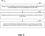
- FIG. 5 illustrates an example of a method 500 for providing a logic XOR function in a superconducting circuit system (e.g., the superconducting XOR-gate system 100).
- a first superconducting logic input signal e.g., the first superconducting logic input signal IN 1
- a second superconducting logic input signal e.g., the second superconducting logic input signal IN 2
- an input superconducting XOR-2 gate e.g., one of the input superconducting XOR gate(s) 104.
- a decision pulse (e.g., the decision pulse PLS) is generated via a pulse generator (e.g., the pulse generator 104) in response to a given phase of a clock signal (e.g., the clock signal CLK).
- the input superconducting XOR-2 gate can perform a logic XOR function based on the decision pulse on the given phase of the clock signal to provide an intermediate superconducting logic output signal (e.g., the intermediate superconducting logic output signal IOx).
- the intermediate superconducting logic output signal and a third superconducting logic input signal are provided to an output superconducting XOR-2 gate (e.g., the superconducting output XOR gate 106).
- the output superconducting XOR-2 gate can perform a logic XOR function based on the decision pulse on the given phase of the clock signal to provide a superconducting logic output signal (e.g., the superconducting logic output signal OUTx).
Landscapes
- Physics & Mathematics (AREA)
- Engineering & Computer Science (AREA)
- Computer Hardware Design (AREA)
- Computing Systems (AREA)
- General Engineering & Computer Science (AREA)
- Mathematical Physics (AREA)
- Logic Circuits (AREA)
- Superconductor Devices And Manufacturing Methods Thereof (AREA)
Abstract
A superconducting XOR-gate system (100) including a pulse generator (104) configured to generate a decision pulse (PLS). The system also includes an input superconducting XOR-2 gate (102) that receives a first superconducting logic input signal (IN1) and a second superconducting logic input signal and is configured to perform a logic XOR function based on the decision pulse (PLS) on a given phase of a clock signal to provide an intermediate superconducting logic output signal (IOx). The system (100) also includes an output superconducting XOR-2 gate (106) that receives the intermediate superconducting logic output signal and a third superconducting logic input signal and is configured to perform a logic XOR function based on the decision pulse on the given phase of the clock signal to provide a superconducting logic output signal (OUTx).
Description
- The present invention relates generally to superconducting circuits, and specifically to a superconducting XOR-gate system.
- Logic gates are an integral aspect of computer processing. Traditional computer processing that implements complementary metal-oxide semiconductor (CMOS) provides for a simplified manner of implementing logic gates using binary signals. However, superconducting technology introduces additional challenges to fabricating logic gates and implementing logic operations. As an example, in wave-pipeline (WPL) superconducting technologies, such as reciprocal quantum logic (RQL), the exclusive-OR (XOR) gate is accomplished in such a way that the maximum input size is two, and each XOR gate is implemented on a different phase boundary of an associated clock signal relative to each other. As a result, XOR gates that require more than two logic inputs operate out-of-phase with respect to each other. However, XOR gates are useful in arithmetic units like multipliers, such that XOR operations that require a larger quantity of logic inputs in typical superconducting circuits increases latency.
- One example describes a superconducting exclusive-OR (XOR) gate system. The system includes a pulse generator configured to generate a decision pulse. The system also includes an input superconducting XOR gate that receives a first superconducting logic input signal and a second superconducting logic input signal and is configured to perform a logic XOR function based on the decision pulse on a given phase of a clock signal to provide an intermediate superconducting logic output signal. The system also includes an output superconducting XOR gate that receives the intermediate superconducting logic output signal and a third superconducting logic input signal and is configured to perform a logic XOR function based on the decision pulse on the given phase of the clock signal to provide a superconducting logic output signal.
- Another example includes a method for providing a logic exclusive-OR (XOR) function in a superconducting circuit system. The method includes providing a first superconducting logic input signal and a second superconducting logic input signal to an input superconducting XOR-2 gate. The method also includes generating a decision pulse via a pulse generator in response to a given phase of a clock signal. The input superconducting XOR-2 gate can perform a logic XOR function based on the decision pulse on the given phase of the clock signal to provide an intermediate superconducting logic output signal. The method further includes providing the intermediate superconducting logic output signal and a third superconducting logic input signal to an output superconducting XOR-2 gate. The output superconducting XOR-2 gate can perform a logic XOR function based on the decision pulse on the given phase of the clock signal to provide a superconducting logic output signal.
- Another example includes a superconducting exclusive-OR (XOR) gate system. The system includes a pulse generator configured to generate a decision pulse and to delay the decision pulse to generate a delayed decision pulse. The system also includes an input superconducting XOR-2 gate that receives a first superconducting logic input signal and a second superconducting logic input signal and is configured to perform a logic XOR function based on the decision pulse on a given phase of a clock signal to provide an intermediate superconducting logic output signal. The system also includes an output superconducting XOR-2 gate that receives the intermediate superconducting logic output signal and a third superconducting logic input signal and is configured to perform a logic XOR function based on the delayed decision pulse on the given phase of the clock signal to provide a superconducting logic output signal.
-
-
FIG. 1 illustrates an example block diagram of a superconducting exclusive-OR (XOR)-N gate system. -
FIG. 2 illustrates an example diagram of XOR gate systems. -
FIG. 3 illustrates an example of a superconducting XOR-3 gate circuit. -
FIG. 4 illustrates an example of a superconducting XOR-4 gate circuit. -
FIG. 5 illustrates an example of a method for performing a logic XOR operation. - The present invention relates generally to superconducting circuits, and specifically to a superconducting exclusive-OR (XOR) gate system. As described herein, the XOR-gate system provides an XOR-function (i.e., an output of a logic-1 in response to non-equal logic inputs) for a plurality N inputs greater than two. The superconducting XOR-gate system includes multiple two-input superconducting XOR gates to form a multi-input (e.g., three-input or four-input) superconducting XOR gate that can perform a logic XOR function on a given one phase of a clock signal. The superconducting XOR-gate system can include a pulse generator that is configured to generate a decision pulse. The pulse generator can include a delay line that can delay the decision pulse to generate a delayed decision pulse. The superconducting XOR-gate system also includes an input superconducting XOR gate that receives a first superconducting logic input signal and a second superconducting logic input signal. As described herein, the term "superconducting logic signal" (e.g., superconducting logic signal, superconducting logic input signal, superconducting logic output signal, etc.) refers to a logic signal that has a first binary logic state corresponding to a superconducting pulse (e.g., a reciprocal quantum logic (RQL) pulse or a single-flux quantum (SFQ) pulse) and has a second binary logic state corresponding to an absence of a superconducting pulse. Therefore, as described hereinafter, the "first logic state" corresponds to the presence of a pulse and the "second logic state" corresponds to the absence of a pulse.
- The input superconductor XOR gate is configured to perform a logic XOR function based on the decision pulse on a given phase of the clock signal to provide an intermediate superconducting logic output signal. The superconducting XOR-gate system also includes an output superconducting XOR gate that receives the intermediate superconducting logic output signal and a third superconducting logic input signal and performs a logic XOR function to generate a superconducting logic output signal based on the delayed decision pulse on the given clock phase. In the example of a three-input superconducting XOR-gate system, the third superconducting logic input signal corresponds to a third input of the three-input superconducting XOR-gate system, such that the three-input superconducting XOR-gate system performs a logic XOR function on the first, second, and third superconducting logic input signals. In the example of a four-input superconducting XOR-gate system, the third superconducting logic input signal can correspond to a second intermediate superconducting logic output signal. Therefore, in the example of the four-input XOR gate, the second intermediate superconducting logic output signal can be generated by a second input superconducting XOR gate that receives a fourth superconducting logic input signal and a fifth superconducting logic input signal as inputs and performs a logic XOR function based on the decision pulse to generate the second intermediate superconducting logic output signal.
-
FIG. 1 illustrates an example block diagram of a superconducting exclusive-OR (XOR)-N gate system 100. The term "XOR-N" refers to a quantity N of superconducting logic input signals, demonstrated in the example ofFIG. 1 as signals IN1 through INN, where N can be a positive integer greater than two. As an example, N can be three or four, such that thesuperconducting XOR-gate system 100 can be a three-input superconducting XOR-gate system or a four-input superconducting XOR-gate system to perform a logic XOR function on the three or four superconducting logic input signals IN1 through INN to generate a single superconducting logic output signal OUTx. - In the example of
FIG. 1 , thesuperconducting XOR-gate system 100 includes at least one input superconducting XOR gate ("INPUT XOR GATE(S)") 102 that receives the superconducting logic input signals IN1 through INN. As a first example, the superconducting XOR gate(s) 102 can include only a singlesuperconducting XOR gate 102 in the example of an XOR-3 gate, such that thesuperconducting XOR-gate system 100 can perform a logic XOR function on three superconducting logic input signals IN1 through IN3. As a second example, the superconducting XOR gate(s) 102 can include twosuperconducting XOR gates 102 in the example of an XOR-4 gate, such that thesuperconducting XOR-gate system 100 can perform a logic XOR function on four superconducting logic input signals IN1 through IN4. As described in greater detail herein, each of the superconducting XOR gate(s) 102 can include storage Josephson junctions at respective inputs and an escape Josephson junction to mitigate pulse propagation between the respective inputs. In the example ofFIG. 1 , each of the input superconducting XOR gate(s) 102 receives a clock signal CLK. - The
superconducting XOR-gate system 100 also includes apulse generator 104 that is configured to generate a decision pulse PLS that is provided to each of the input superconducting XOR gate(s) 102. Therefore, each of the input superconducting XOR gate(s) 102 performs a logic XOR function on a set of the inputs IN1 through INN based on the decision pulse PLS, as described in greater detail herein. As an example, thepulse generator 104 can include a Josephson junction having a low critical current, such that the Josephson junction can be triggered by the clock signal CLK. Therefore, the decision pulse PLS can correspond to a superconducting pulse (e.g., an RQL pulse) that is provided to the input superconducting XOR gate(s) 102 to bias a decision Josephson junction. As a result, the input superconducting XOR gate(s) 102 can perform a logic XOR function on a set of the inputs IN1 through INN based on the decision pulse PLS to generate at least one intermediate superconducting logic output signal, demonstrated in the example ofFIG. 1 as a signal IOx. For example, thepulse generator 104 can generate a first decision pulse PLS_1 for the first inputsuperconducting XOR gate 102 and a second decision pulse PLS_2 for the second inputsuperconducting XOR gate 102 for thesuperconducting XOR-gate system 100 being arranged as an XOR-4 gate. - The
superconducting XOR-gate system 100 also includes an outputsuperconducting XOR gate 106 that receives the intermediate superconducting logic output signal(s) IOx. In the example of thesuperconducting XOR-gate system 100 being arranged as an XOR-3 gate, the outputsuperconducting XOR gate 106 can also receive one of the superconducting input logic signals IN1 through INN (e.g., the superconducting input logic signal IN3). Therefore, the outputsuperconducting XOR gate 106 can perform a logic XOR function on the superconducting logic input signal IN3 and the intermediate superconducting logic output signal IOx. In the example of thesuperconducting XOR-gate system 100 being arranged as an XOR-4 gate, the outputsuperconducting XOR gate 106 can receive a first intermediate superconducting logic output signal IOX1 from the first inputsuperconducting XOR gate 102 and a second intermediate superconducting logic output signal IOX2 from the second inputsuperconducting XOR gate 102. Therefore, the outputsuperconducting XOR gate 106 can perform a logic XOR function on the first and second intermediate superconducting logic output signals IOX1 and IOX2. The outputsuperconducting XOR gate 106 can be arranged substantially the same as the input superconducting XOR gate(s) 102. In the example ofFIG. 1 , the outputsuperconducting XOR gate 106 receives the clock signal CLK. - In the example of
FIG. 1 , thepulse generator 104 includes adelay line 108 that is configured to generate a delayed version of the decision pulse PLS, demonstrated as a signal DPLS. The delayed decision pulse DPLS is provided to the outputsuperconducting XOR gate 106. Therefore, similar to as described above, the delayed decision pulse DPLS can correspond to a superconducting pulse (e.g., an RQL pulse) that is provided to the outputsuperconducting XOR gate 106 to bias a decision Josephson junction. As a result, the outputsuperconducting XOR gate 106 can perform a logic XOR function on the intermediate superconducting logic output signal IOx and another signal (e.g., the input signal IN3 or a second intermediate superconducting logic output signal IOX2) based on the delayed decision pulse DPLS to generate the superconducting output logic signal OUTx. - As an example, the
delay line 108 can include a delay buffer that is formed by at least one Josephson transmission line (JTL) through which the decision pulse PLS propagates to generate the delayed decision pulse DPLS. Therefore, the propagation of the decision pulse PLS through thedelay line 108 can result in the delayed decision pulse DPLS arriving at the outputsuperconducting XOR gate 106 slightly later in time than the decision pulse PLS arrives at the input superconducting XOR gate(s) 102. Therefore, the input superconducting XOR gate(s) 102 can perform the respective logic XOR function at a time prior to the arrival of the delayed decision pulse DPLS to the outputsuperconducting XOR gate 106. - As a result, the superconducting logic inputs to the output
superconducting XOR gate 106 can arrive prior to the delayed decision pulse DPLS, thereby facilitating the logic XOR function by the outputsuperconducting XOR gate 106 in a manner that mitigates timing errors (e.g., race conditions) associated with the logic XOR function of the outputsuperconducting XOR gate 106. Furthermore, because the delayed decision pulse DPLS is only very slightly delayed relative to the decision pulse PLS (e.g., by propagation of the delay pulse PLS through at least one JTL), the input superconducting XOR gate(s) 102 and the outputsuperconducting XOR gate 106 can perform the respective logic XOR functions on the same phase of the clock signal CLK. Therefore, unlike typical superconducting XOR gates having greater than two inputs, the superconductingXOR-gate system 100 can perform the logic XOR-N function on a single clock phase, as opposed to over multiple phases of the clock signal (e.g., the output being out-of-phase of the inputs by 90° or more). Accordingly, the superconductingXOR-gate system 100 can perform logic XOR functions at a lower latency than typical superconducting XOR-N gates. -
FIG. 2 illustrates an example diagram 200 of XOR gate systems. The diagram 200 includes a first superconductingXOR-gate system 202 and a secondsuperconducting XOR-gate system 204. The first superconductingXOR-gate system 202 is demonstrated as an XOR-3 logic gate system that performs a logic XOR function on a set of three inputs, demonstrated as IN1 through IN3. The secondsuperconducting XOR-gate system 204 is demonstrated as an XOR-4 logic gate system that performs a logic XOR function on a set of four inputs, demonstrated as IN1 through IN4. Each of the superconductingXOR-gate systems XOR-gate system 100 in the example ofFIG. 1 . Therefore, reference is to be made to the example ofFIG. 1 in the following description of the example ofFIG. 2 . In the example ofFIG. 2 , the logic XOR gates are demonstrated in the traditional notation for logic XOR gates. However, the logic XOR gates of the example ofFIG. 2 correspond to superconducting XOR gates that operate on the clock signal CLK (e.g., an RQL clock signal), as described in greater detail herein. - The first superconducting
XOR-gate system 202 includes apulse generator 206, aninput XOR gate 208, and anoutput XOR gate 210. Thepulse generator 206 is demonstrated as generating a decision pulse PLS that is provided to theinput XOR gate 208 and a delayed decision pulse DPLS that is provided to theoutput XOR gate 210. Theinput XOR gate 208 receives a first superconducting logic input signal IN1 and a second superconducting logic input signal IN2, such that theinput XOR gate 208 performs a logic XOR function on the first and second superconducting logic input signals IN1 and IN2 based on the decision pulse PLS to generate an intermediate superconducting logic output signal IOx. Theoutput XOR gate 208 receives the intermediate superconducting logic output signal IOx and a third superconducting logic input signal IN3, such that theoutput XOR gate 210 performs a logic XOR function on the third superconducting logic input signal IN3 and the intermediate superconducting logic output signal IOx based on the delayed decision pulse DPLS to generate a superconducting logic output signal OUTx. - As described previously, the delayed decision pulse DPLS can be provided to the
output XOR gate 210 subsequent to the decision pulse PLS being provided to theinput XOR gate 208. As a result, theinput XOR gate 208 can perform the logic XOR function prior to theoutput XOR gate 210, such that the logic state of the intermediate superconducting logic output signal IOx can be set prior to the logic XOR function performed by theoutput XOR gate 210. Accordingly, the superconductingXOR-gate system 202 can perform a logic XOR-3 function on a single phase of the clock signal CLK. - The second
superconducting XOR-gate system 204 includes apulse generator 212, a firstinput XOR gate 214, a secondinput XOR gate 216, and anoutput XOR gate 218. Thepulse generator 212 is demonstrated as generating a first decision pulse PLS_1 that is provided to the firstinput XOR gate 214, a second decision pulse PLS_2 that is provided to the secondinput XOR gate 216, and a delayed decision pulse DPLS that is provided to theoutput XOR gate 218. The firstinput XOR gate 214 receives a first superconducting logic input signal IN1 and a second superconducting logic input signal IN2, such that the firstinput XOR gate 214 performs a logic XOR function on the first and second superconducting logic input signals IN1 and IN2 based on the first decision pulse PLS_1 to generate a first intermediate superconducting logic output signal IOX1. The secondinput XOR gate 216 receives a third superconducting logic input signal IN3 and a fourth superconducting logic input signal IN4, such that the secondinput XOR gate 216 performs a logic XOR function on the third and fourth superconducting logic input signals IN3 and IN4 based on the second decision pulse PLS_2 to generate a second intermediate superconducting logic output signal IOX1. Theoutput XOR gate 218 receives the first and second intermediate superconducting logic output signals IOX1 and IOX2, such that theoutput XOR gate 210 performs a logic XOR function on first and second intermediate superconducting logic output signals IOX1 and IOX2 based on the delayed decision pulse DPLS to generate a superconducting logic output signal OUTx. - As described previously, the delayed decision pulse DPLS can be provided to the
output XOR gate 218 subsequent to the first and second decision pulses PLS_1 and PLS_2 being provided to the respective first and secondinput XOR gates input XOR gates output XOR gate 218, such that the logic state of the respective first and second intermediate superconducting logic output signals IOX1 and IOX2 can be set prior to the logic XOR function performed by theoutput XOR gate 218. Accordingly, the superconductingXOR-gate system 204 can perform a logic XOR-4 function on a single phase of the clock signal CLK. -
FIG. 3 illustrates an example of a superconducting XOR-3gate circuit 300. The superconducting XOR-3gate circuit 300 can correspond to the superconductingXOR-gate system 100 or the superconductingXOR-gate system 202 in the respective examples ofFIGS. 1 and 2 . Therefore, reference is to be made to the examples ofFIGS. 1 and 2 in the following description of the example ofFIG. 3 . - The superconducting XOR-3
gate circuit 300 includes apulse generator 302, an inputsuperconducting XOR gate 304, and an outputsuperconducting XOR gate 306. Thepulse generator 306 includes a Josephson junction JPLS that is coupled to the clock signal CLK and that is fabricated to have a critical current that is relatively lower than other Josephson junctions that are biased by the clock signal CLK. Therefore, in response to a given phase of the clock signal CLK (e.g., a bias provided by the clock signal CLK), the Josephson junction JPLS triggers to generate the decision pulse PLS. The decision pulse PLS propagates through a JTL stage formed by an inductor L1, a Josephson junction J1, and an inductor L2, and through another JTL stage formed by an inductor L3, a Josephson junction J2, and an inductor L4. The JTL stages are biased by the clock signal CLK. In response to the Josephson junction J2 triggering, the decision pulse PLS is split, such that a first decision pulse PLS is provided through the inductor L4 to an escape Josephson junction JESC1 and a second decision pulse PLS_D is provided to adelay line 308. - The input
superconducting XOR gate 304 receives a first superconducting logic input signal IN1 at afirst input 310 and a second superconducting logic input signal IN2 at asecond input 312. Thefirst input 310 includes a JTL stage formed by an inductor L5, a storage Josephson junction Jsi, and an inductor L6. Similarly, thesecond input 312 includes a JTL stage formed by an inductor L7, a storage Josephson junction JS2, and an inductor L8. The storage Josephson junctions Jsi and JS2 are unbiased. Therefore, the storage Josephson junctions Jsi and JS2 are each configured to trigger in response to the first logic state (e.g., a pulse) of the respective one of the superconducting logic input signals IN1 and IN2, but to not trigger in response to the first logic state of the other of the superconducting logic input signals IN1 and IN2. - The superconducting logic input signals IN1 and IN2 are provided to an escape Josephson junction JESC2 that is coupled to a grounded inductor LRST1 and a decision Josephson junction JD1. In response to a single one of the superconducting logic input signals IN1 and IN2 having the first logic state, the respective pulse introduces a flux-quantum into a decision loop formed by the decision Josephson junction JD1 and the respective one of the storage Josephson junctions Jsi and JS2. The flux quantum can be insufficient to trigger the escape Josephson junction JESC2, but can be sufficient to trigger the decision Josephson junction JD1 in combination with the decision pulse PLS. As a result, the intermediate superconducting logic output signal IOX can propagate as a pulse (e.g., the first logic state) from the decision Josephson junction JD1 through an inductor L9 and an inductor L10 to trigger a Josephson junction J3 via a bias from the respective phase of the clock signal CLK. The grounded inductor LRST1, having a significantly higher inductance than the remaining inductors in the JTL stages in the input
superconducting XOR gate 304, can thus operate to reset the flux quantum in the decision loop. - In response to both of the superconducting logic input signals IN1 and IN2 having the first logic state, the critical current of the escape Josephson junction JESC2 is exceeded, causing the escape Josephson junction JESC2 to trigger. As a result, the escape Josephson junction JESC2 annihilates the flux quantum in the decision loop. Alternatively, in response to both of the superconducting logic input signals IN1 and IN2 having the second logic state (e.g., no pulse), no flux quantum is introduced into the decision loop. In either of the same logic state examples, the decision pulse PLS triggers the escape Josephson junction JESC1 in the
pulse generator 302, thus annihilating the decision pulse PLS. As a result, no pulse propagates from the decision Josephson junction JD1 through the inductor L9 and the inductor L10 (and the Josephson junction J3 does not trigger) based on the intermediate superconducting logic output signal IOX having the second logic state. Therefore, as described above, the inputsuperconducting XOR gate 304 performs a logic XOR function on the first and second superconducting logic input signals IN1 and IN2 based on the decision pulse PLS to generate an intermediate superconducting logic output signal IOX having either the first or the second logic state. - As described above regarding the
pulse generator 302, a second decision pulse PLS_D is provided to thedelay line 308. Thedelay line 308 includes adelay buffer 314 that is configured to provide a propagation delay of the second decision pulse PLS_D. For example, thedelay buffer 314 can be formed by a sequence of JTL stages. Thedelay line 308 also includes a JTL stage formed by an inductor L11, a Josephson junction J4, and an inductor L12, and another JTL stage formed by an inductor L13, a Josephson junction J5, and an inductor L14. The JTL stages can be part of thedelay buffer 314, or can be separate from the JTL stages associated with thedelay buffer 314. Thedelay line 308 can thus generate the delayed decision pulse DPLS based on the second decision pulse PLS_D. The delayed decision pulse DPLS can thus be provided to the outputsuperconducting XOR gate 306 via an escape Josephson junction JESC3 in a manner that is delayed relative to the decision pulse PLS provided to the inputsuperconducting XOR gate 304. As an example, the quantity of JTL stages of thedelay buffer 314 can be sufficient to delay the arrival of the delayed decision pulse DPLS to occur sufficiently after the time that the inputsuperconducting XOR gate 304 performs the logic XOR function and provides the resultant intermediate superconducting logic output signal IOX. - The output
superconducting XOR gate 308 receives the intermediate superconducting logic output signal IOx at afirst input 316 and a third superconducting logic input signal IN3 at asecond input 318. Thefirst input 316 includes a JTL stage formed by an inductor L15, a storage Josephson junction JS3, and an inductor L16. Similarly, thesecond input 318 includes a JTL stage formed by an inductor L17, a storage Josephson junction JS4, and an inductor L18. The storage Josephson junctions JS3 and JS4 are unbiased, and therefore are fabricated to have a relatively low critical current (e.g., relative to the JTL stages associated with thepulse generator 306 and/or thesuperconducting XOR gates 304 and 306). Therefore, the storage Josephson junctions JS3 and JS4 are each configured to trigger in response to the first logic state (e.g., a pulse) of the respective one of the intermediate superconducting logic output signal IOx and the superconducting logic input signal IN3, but to not trigger in response to the first logic state of the other of the intermediate superconducting logic output signal IOx and the superconducting logic input signal IN3. - The intermediate superconducting logic output signal IOx and the superconducting logic input signal IN3 are provided to an escape Josephson junction JESC4 that is coupled to a grounded inductor LRST2 and a decision Josephson junction JD2. In response to a single one of the intermediate superconducting logic output signal IOx and the superconducting logic input signal IN3 having the first logic state, the respective pulse introduces a flux-quantum into a decision loop formed by the decision Josephson junction JD2 and the respective one of the storage Josephson junctions JS3 and JS4. The flux quantum can be insufficient to trigger the escape Josephson junction JESC4, but can be sufficient to trigger the decision Josephson junction JD2 in combination with the delayed decision pulse DPLS. As a result, the superconducting logic output signal OUTx can propagate as a pulse (e.g., the first logic state) from the decision Josephson junction JD2 through an inductor L19 and an inductor L20 to trigger a Josephson junction J6 via a bias from the respective phase of the clock signal CLK. The grounded inductor LRST2, having a significantly higher inductance than the remaining inductors in the JTL stages in the output
superconducting XOR gate 308, can thus operate to reset the flux quantum in the decision loop. - In response to both of the intermediate superconducting logic output signal IOx and the superconducting logic input signal IN3 having the first logic state, the critical current of the escape Josephson junction JESC4 is exceeded, causing the escape Josephson junction JESC4 to trigger. As a result, the escape Josephson junction JESC4 annihilates the flux quantum in the decision loop. Alternatively, in response to both of the intermediate superconducting logic output signal IOx and the superconducting logic input signal IN3 having the second logic state (e.g., no pulse), no flux quantum is introduced into the decision loop. In either of the same logic state examples, the delayed decision pulse DPLS triggers the escape Josephson junction JESC3 in the
delay line 308, thus annihilating the delayed decision pulse DPLS. As a result, no pulse propagates from the decision Josephson junction JD2 through the inductor L19 and the inductor L20 (and the Josephson junction J6 does not trigger) based on the superconducting logic output signal OUTx having the second logic state. Therefore, as described above, the outputsuperconducting XOR gate 306 performs a logic XOR function on the intermediate superconducting logic output signal IOx and the superconducting logic input signal IN3 based on the delayed decision pulse DPLS to generate the superconducting logic output signal OUTx having either the first or the second logic state. - As a result, as described above, the superconducting logic inputs to the output
superconducting XOR gate 306 can arrive prior to the delayed decision pulse DPLS, thereby facilitating the logic XOR function by the outputsuperconducting XOR gate 306 in a manner that mitigates timing errors (e.g., race conditions) associated with the logic XOR function of the outputsuperconducting XOR gate 306. Furthermore, because the delayed decision pulse DPLS is only very slightly delayed relative to the decision pulse PLS (e.g., by propagation of the second delay pulse PLS D through the delay buffer 314), the inputsuperconducting XOR gate 304 and the outputsuperconducting XOR gate 306 can perform the respective logic XOR functions on the same phase of the clock signal CLK. -
FIG. 4 illustrates an example of a superconducting XOR-4gate circuit 400. The superconducting XOR-4gate circuit 400 can correspond to the superconductingXOR-gate system 100 or the superconductingXOR-gate system 202 in the respective examples ofFIGS. 1 and 2 . Therefore, reference is to be made to the examples ofFIGS. 1 and 2 in the following description of the example ofFIG. 4 . - The superconducting XOR-4
gate circuit 400 includes apulse generator 402, a first input superconductingXOR gate 404, a second input superconductingXOR gate 406, and an outputsuperconducting XOR gate 408. Thepulse generator 408 includes a Josephson junction JPLS that is fabricated to have a relatively low critical current (e.g., relative to the JTL stages associated with thepulse generator 408 and/or thesuperconducting XOR gates 404 and 408). The Josephson junction JPLS is coupled to the clock signal CLK, such that, in response to a given phase of the clock signal (e.g., a bias provided by the clock signal CLK), the Josephson junction JPLS triggers to generate the decision pulse PLS. The decision pulse PLS propagates through a JTL stage formed by an inductor L1, a Josephson junction J1, and an inductor L2, and through another JTL stage formed by an inductor L3, a Josephson junction J2, and an inductor L4. The JTL stages are biased by the clock signal CLK. In response to the Josephson junction J2 triggering, the decision pulse PLS is split, such that a first decision pulse PLS_1 is provided through an escape Josephson junction JESC1 to the firstsuperconducting XOR gate 304, a second decision pulse PLS_2 is provided through an escape Josephson junction JESC2 to the secondsuperconducting XOR gate 306, and a third decision pulse PLS D is provided to adelay line 410. - The first input superconducting
XOR gate 404 receives a first superconducting logic input signal IN1 at afirst input 412 and a second superconducting logic input signal IN2 at asecond input 414. Thefirst input 412 includes a JTL stage formed by an inductor L5, a storage Josephson junction Jsi, and an inductor L6. Similarly, thesecond input 414 includes a JTL stage formed by an inductor L7, a storage Josephson junction JS2, and an inductor L8. The storage Josephson junctions JS1 and JS2 are unbiased, and therefore are fabricated to have a relatively low critical current (e.g., relative to the JTL stages associated with thepulse generator 408 and/or thesuperconducting XOR gates 404 and 408). Therefore, the storage Josephson junctions Jsi and JS2 are each configured to trigger in response to the first logic state (e.g., a pulse) of the respective one of the superconducting logic input signals IN1 and IN2, but to not trigger in response to the first logic state of the other of the superconducting logic input signals IN1 and IN2. - The superconducting logic input signals IN1 and IN2 are provided to an escape Josephson junction JESC3 that is coupled to a grounded inductor LRST1 and a decision Josephson junction JD1. In response to a single one of the superconducting logic input signals IN1 and IN2 having the first logic state, the respective pulse introduces a flux-quantum into a decision loop formed by the decision Josephson junction JD1 and the respective one of the storage Josephson junctions Jsi and JS2. The flux quantum can be insufficient to trigger the escape Josephson junction JESC2, but can be sufficient to trigger the decision Josephson junction JD1 in combination with the first decision pulse PLS_1. As a result, a first intermediate superconducting logic output signal IOX1 can propagate as a pulse (e.g., the first logic state) from the decision Josephson junction JD1 through an inductor L9 and an inductor L10 to trigger a Josephson junction J3 via a bias from the respective phase of the clock signal CLK. The grounded inductor LRST1, having a significantly higher inductance than the remaining inductors in the JTL stages in the first input superconducting
XOR gate 404, can thus operate to reset the flux quantum in the decision loop. - In response to both of the superconducting logic input signals IN1 and IN2 having the first logic state, the critical current of the escape Josephson junction JESC3 is exceeded, causing the escape Josephson junction JESC3 to trigger. As a result, the escape Josephson junction JESC3 annihilates the flux quantum in the decision loop. Alternatively, in response to both of the superconducting logic input signals IN1 and IN2 having the second logic state (e.g., no pulse), no flux quantum is introduced into the decision loop. In either of the same logic state examples, the first decision pulse PLS_1 triggers the escape Josephson junction JESC1 in the
pulse generator 402, thus annihilating the first decision pulse PLS_1. As a result, no pulse propagates from the decision Josephson junction JD1 through the inductor L9 and the inductor L10 (and the Josephson junction J3 does not trigger) based on the first intermediate superconducting logic output signal IOX1 having the second logic state. Therefore, as described above, the first input superconductingXOR gate 404 performs a logic XOR function on the first and second superconducting logic input signals IN1 and IN2 based on the first decision pulse PLS_1 to generate a first intermediate superconducting logic output signal IOX1 having either the first or the second logic state. - The second input superconducting
XOR gate 406 receives a third superconducting logic input signal IN3 at afirst input 416 and a second superconducting logic input signal IN2 at asecond input 418. Thefirst input 416 includes a JTL stage formed by an inductor L11, a storage Josephson junction JS3, and an inductor L12. Similarly, thesecond input 418 includes a JTL stage formed by an inductor L13, a storage Josephson junction JS4, and an inductor L14. The storage Josephson junctions JS3 and JS4 are unbiased, and therefore are fabricated to have a relatively low critical current (e.g., relative to the JTL stages associated with thepulse generator 402 and/or thesuperconducting XOR gates - The superconducting logic input signals IN3 and IN4 are provided to an escape Josephson junction JESC4 that is coupled to a grounded inductor LRST2 and a decision Josephson junction JD2. In response to a single one of the superconducting logic input signals IN3 and IN4 having the first logic state, the respective pulse introduces a flux-quantum into a decision loop formed by the decision Josephson junction JD2 and the respective one of the storage Josephson junctions JS3 and JS4. The flux quantum can be insufficient to trigger the escape Josephson junction JESC3, but can be sufficient to trigger the decision Josephson junction JD2 in combination with the second decision pulse PLS_2. As a result, a second intermediate superconducting logic output signal IOX2 can propagate as a pulse (e.g., the first logic state) from the decision Josephson junction JD2 through an inductor L15 and an inductor L16 to trigger a Josephson junction J4 via a bias from the respective phase of the clock signal CLK. The grounded inductor LRST2, having a significantly higher inductance than the remaining inductors in the JTL stages in the second input superconducting
XOR gate 406, can thus operate to reset the flux quantum in the decision loop. - In response to both of the superconducting logic input signals IN3 and IN4 having the first logic state, the critical current of the escape Josephson junction JESC4 is exceeded, causing the escape Josephson junction JESC4 to trigger. As a result, the escape Josephson junction JESC4 annihilates the flux quantum in the decision loop. Alternatively, in response to both of the superconducting logic input signals IN3 and IN4 having the second logic state (e.g., no pulse), no flux quantum is introduced into the decision loop. In either of the same logic state examples, the second decision pulse PLS_2 triggers the escape Josephson junction JESC2 in the
pulse generator 402, thus annihilating the second decision pulse PLS_2. As a result, no pulse propagates from the decision Josephson junction JD2 through the inductor L15 and the inductor L16 (and the Josephson junction J4 does not trigger) based on the second intermediate superconducting logic output signal IOX2 having the second logic state. Therefore, as described above, the second input superconductingXOR gate 406 performs a logic XOR function on the third and fourth superconducting logic input signals IN3 and IN4 based on the second decision pulse PLS_2 to generate a second intermediate superconducting logic output signal IOX2 having either the first or the second logic state. - As described above regarding the
pulse generator 402, a third decision pulse PLS_D is provided to thedelay line 410. Thedelay line 410 includes adelay buffer 420 that is configured to provide a propagation delay of the third decision pulse PLS_D. For example, thedelay buffer 420 can be formed by a sequence of JTL stages. Thedelay line 410 also includes a JTL stage formed by an inductor L17, a Josephson junction J5, and an inductor L18, and another JTL stage formed by an inductor L19, a Josephson junction J6, and an inductor L20. The JTL stages can be part of thedelay buffer 420, or can be separate from the JTL stages associated with thedelay buffer 420. Thedelay line 410 can thus generate the delayed decision pulse DPLS based on the third decision pulse PLS_D. The delayed decision pulse DPLS can thus be provided to the outputsuperconducting XOR gate 408 via an escape Josephson junction JESC5 in a manner that is delayed relative to the first and second decision pulses PLS_1 and PLS_2 provided to the respective first and second input superconductingXOR gates delay buffer 420 can be sufficient to delay the arrival of the delayed decision pulse DPLS to occur sufficiently after the time that the first and second input superconductingXOR gates - The output
superconducting XOR gate 410 receives the first intermediate superconducting logic output signal IOX1 at afirst input 422 and the second intermediate superconducting logic output signal IOX2 at asecond input 424. Thefirst input 422 includes a JTL stage formed by an inductor L21, a storage Josephson junction JS5, and an inductor L22. Similarly, thesecond input 424 includes a JTL stage formed by an inductor L23, a storage Josephson junction JS6, and an inductor L24. The storage Josephson junctions JS5 and JS6 are unbiased, and therefore are fabricated to have a relatively low critical current (e.g., relative to the JTL stages associated with thepulse generator 408 and/or thesuperconducting XOR gates - The first intermediate superconducting logic output signal IOX1 and the second intermediate superconducting logic output signal IOX2 are provided to an escape Josephson junction JESC6 that is coupled to a grounded inductor LRST3 and a decision Josephson junction JD3. In response to a single one of the first and second intermediate superconducting logic output signals IOX1 and IOX2 having the first logic state, the respective pulse introduces a flux-quantum into a decision loop formed by the decision Josephson junction JD3 and the respective one of the storage Josephson junctions JS5 and JS6. The flux quantum can be insufficient to trigger the escape Josephson junction JESC6, but can be sufficient to trigger the decision Josephson junction JD3 in combination with the delayed decision pulse DPLS. As a result, the superconducting logic output signal OUTx can propagate as a pulse (e.g., the first logic state) from the decision Josephson junction JD3 through an inductor L25 and an inductor L26 to trigger a Josephson junction J7 via a bias from the respective phase of the clock signal CLK. The grounded inductor LRST3, having a significantly higher inductance than the remaining inductors in the JTL stages in the output
superconducting XOR gate 410, can thus operate to reset the flux quantum in the decision loop. - In response to both of the first and second intermediate superconducting logic output signals IOX1 and IOX2 having the first logic state, the critical current of the escape Josephson junction JESC6 is exceeded, causing the escape Josephson junction JESC6 to trigger. As a result, the escape Josephson junction JESC6 annihilates the flux quantum in the decision loop. Alternatively, in response to both of the first and second intermediate superconducting logic output signals IOX1 and IOX2 having the second logic state (e.g., no pulse), no flux quantum is introduced into the decision loop. In either of the same logic state examples, the delayed decision pulse DPLS triggers the escape Josephson junction JESC5 in the
delay line 410, thus annihilating the delayed decision pulse DPLS. As a result, no pulse propagates from the decision Josephson junction JD3 through the inductor L25 and the inductor L26 (and the Josephson junction J7 does not trigger) based on the superconducting logic output signal OUTx having the second logic state. Therefore, as described above, the outputsuperconducting XOR gate 408 performs a logic XOR function on the first and second intermediate superconducting logic output signals IOX1 and IOX2 based on the delayed decision pulse DPLS to generate the superconducting logic output signal OUTx having either the first or the second logic state. - As a result, as described above, the superconducting logic inputs to the output
superconducting XOR gate 408 can arrive prior to the delayed decision pulse DPLS, thereby facilitating the logic XOR function by the outputsuperconducting XOR gate 408 in a manner that mitigates timing errors (e.g., race conditions) associated with the logic XOR function of the outputsuperconducting XOR gate 408. Furthermore, because the delayed decision pulse DPLS is only very slightly delayed relative to the first and second decision pulses PLS_1 and PLS_2 (e.g., by propagation of the second delay pulse PLS_D through the delay buffer 420), the first input superconductingXOR gate 404, the second input superconductingXOR gate 406, and the outputsuperconducting XOR gate 408 can perform the respective logic XOR functions on the same phase of the clock signal CLK. - In view of the foregoing structural and functional features described above, a methodology in accordance with various aspects of the present invention will be better appreciated with reference to
FIG. 5 . While, for purposes of simplicity of explanation, the methodology ofFIG. 5 is shown and described as executing serially, it is to be understood and appreciated that the present invention is not limited by the illustrated order, as some aspects could, in accordance with the present invention, occur in different orders and/or concurrently with other aspects from that shown and described herein. Moreover, not all illustrated features may be required to implement a methodology in accordance with an aspect of the present invention. -
FIG. 5 illustrates an example of amethod 500 for providing a logic XOR function in a superconducting circuit system (e.g., the superconducting XOR-gate system 100). At 502, a first superconducting logic input signal (e.g., the first superconducting logic input signal IN1) and a second superconducting logic input signal (e.g., the second superconducting logic input signal IN2) are provided to an input superconducting XOR-2 gate (e.g., one of the input superconducting XOR gate(s) 104). At 504, a decision pulse (e.g., the decision pulse PLS) is generated via a pulse generator (e.g., the pulse generator 104) in response to a given phase of a clock signal (e.g., the clock signal CLK).. The input superconducting XOR-2 gate can perform a logic XOR function based on the decision pulse on the given phase of the clock signal to provide an intermediate superconducting logic output signal (e.g., the intermediate superconducting logic output signal IOx). At 506, the intermediate superconducting logic output signal and a third superconducting logic input signal (e.g., the third superconducting logic input signal IN3 or the second intermediate superconducting logic output signal IOX2) are provided to an output superconducting XOR-2 gate (e.g., the superconducting output XOR gate 106). The output superconducting XOR-2 gate can perform a logic XOR function based on the decision pulse on the given phase of the clock signal to provide a superconducting logic output signal (e.g., the superconducting logic output signal OUTx). - What have been described above are examples of the invention. It is, of course, not possible to describe every conceivable combination of components or methodologies for purposes of describing the invention, but one of ordinary skill in the art will recognize that many further combinations and permutations of the invention are possible. Accordingly, the invention is intended to embrace all such alterations, modifications, and variations that fall within the scope of this application, including the appended claims. Additionally, where the disclosure or claims recite "a," "an," "a first," or "another" element, or the equivalent thereof, it should be interpreted to include one or more than one such element, neither requiring nor excluding two or more such elements. As used herein, the term "includes" means includes but not limited to, and the term "including" means including but not limited to. The term "based on" means based at least in part on.
- Example of the present invention may also include embodiments as described in the following clauses:
- A. 1 A superconducting XOR-gate system comprising:
- a pulse generator configured to generate a decision pulse and to delay the decision pulse to generate a delayed decision pulse;
- an input superconducting XOR-2 gate that receives a first superconducting logic input signal and a second superconducting logic input signal and is configured to perform a logic XOR function based on the decision pulse on a given phase of a clock signal to provide an intermediate superconducting logic output signal; and an output superconducting XOR-2 gate that receives the intermediate superconducting logic output signal and a third superconducting logic input signal and is configured to perform a logic XOR function based on the delayed decision pulse on the given phase of the clock signal to provide a superconducting logic output signal.
- A. 2 The system of clause A. 1, wherein the pulse generator comprises a delay line comprising a delay buffer, the delay buffer comprising at least one Josephson transmission line to generate the delayed decision pulse.
- A.3 The system of clause A.1 or A.2, wherein the first XOR-2 gate comprises a first input stage that receives the first superconducting logic input signal and a second input stage that receives the second superconducting logic input signal, wherein the second XOR-2 gate comprises a third input stage that receives the third superconducting logic input signal and a fourth input stage that receives the intermediate superconducting logic output signal, wherein each of the first, second, third, and fourth input stages comprises a storage Josephson junction that is not biased by the clock signal.
- A. 4 The system of any proceeding clause, wherein the first, second, and third superconducting logic input signals are provided as Reciprocal Quantum Logic (RQL) pulse, such that the XOR-2 gate system is configured to provide the superconducting logic output signal as an RQL pulse.
- A. 5 The system of any proceeding clause, wherein the input superconducting XOR-2 gate is configured as a first input superconducting XOR-2 gate to perform the logic XOR function to provide a first intermediate superconducting logic output signal, wherein the output superconducting XOR-2 gate receives the first intermediate superconducting logic output signal and the third superconducting logic input signal corresponding to a second intermediate superconducting logic output signal to perform the logic XOR function to provide the superconducting logic output signal, the system further comprising a second input superconducting XOR-2 gate that receives a fourth superconducting logic input signal and a fifth superconducting logic input signal and is configured to perform a logic XOR function based on the decision pulse on the given phase of the clock signal to provide the second intermediate superconducting logic output signal.
Claims (15)
- A superconducting XOR-gate system comprising:a pulse generator configured to generate a decision pulse;an input superconducting XOR gate that receives a first superconducting logic input signal and a second superconducting logic input signal and is configured to perform a logic XOR function based on the decision pulse on a given phase of a clock signal to provide an intermediate superconducting logic output signal; andan output superconducting XOR gate that receives the intermediate superconducting logic output signal and a third superconducting logic input signal and is configured to perform a logic XOR function based on the decision pulse on the given phase of the clock signal to provide a superconducting logic output signal.
- The system of claim 1, wherein the pulse generator comprises a delay line to generate a delayed decision pulse, wherein the output superconducting XOR gate is configured to perform the logic XOR function based on the delayed decision pulse on the given phase of the clock signal.
- The system of claim 2, wherein the delay line comprises a delay buffer, the delay buffer comprising at least one Josephson transmission line.
- The system of any proceeding claim, wherein the first XOR gate comprises a first input stage that receives the first superconducting logic input signal and a second input stage that receives the second superconducting logic input signal, wherein the second XOR gate comprises a third input stage that receives the third superconducting logic input signal and a fourth input stage that receives the intermediate superconducting logic output signal, wherein each of the first, second, third, and fourth input stages comprises a storage Josephson junction that is not biased by the clock signal.
- The system of any proceeding claim, wherein the input superconducting XOR gate comprises a first escape Josephson junction and the output superconducting XOR gate comprises a second escape Josephson junction, wherein the first escape Josephson junction is configured to trigger in response to both the first and second superconducting logic input signals being provided as pulse signals to result in the intermediate superconducting logic output signal being provided as a non-pulse signal, wherein the second Josephson junction is configured to trigger in response to both the third superconducting logic input signal and the intermediate superconducting logic output signal being provided as pulse signals to result in the superconducting logic output signal being provided as a non-pulse signal.
- The system of claim 1, wherein the first, second, and third superconducting logic input signals are provided as Reciprocal Quantum Logic (RQL) pulse, such that the XOR gate system is configured to provide the superconducting logic output signal as an RQL pulse.
- The system of any proceeding claim, wherein the input superconducting XOR gate comprises a first grounded inductor coupled to a first decision Josephson junction that is biased by the decision pulse and the output superconducting XOR gate comprises a second grounded inductor coupled to a second decision Josephson junction that is biased by the decision pulse, wherein the first and second grounded inductors have an inductance value that is greater than Josephson transmission lines (JTLs) associated with the first and output superconducting XOR gates to facilitate reset of the respective first and second decision Josephson junctions.
- The system of any preceding claim, wherein the input superconducting XOR gate is configured as a first input superconducting XOR gate to perform the logic XOR function to provide a first intermediate superconducting logic output signal, wherein the output superconducting XOR gate receives the first intermediate superconducting logic output signal and the third superconducting logic input signal corresponding to a second intermediate superconducting logic output signal to perform the logic XOR function to provide the superconducting logic output signal, the system further comprising a second input superconducting XOR gate that receives a fourth superconducting logic input signal and a fifth superconducting logic input signal and is configured to perform a logic XOR function based on the decision pulse on the given phase of the clock signal to provide the second intermediate superconducting logic output signal.
- The system of any proceeding claim, wherein the pulse generator comprises a first Josephson junction to which the clock signal is provided and at least one Josephson transmission line each comprising at least one second Josephson junction to which the clock signal is provided, wherein the first Josephson junction has a critical current that is less than the at least one second Josephson junction.
- The system of any proceeding claim, wherein each of the input superconducting XOR gate and the output superconducting XOR gate are arranged as XOR-2 gates.
- A method for providing a logic XOR function in a superconducting circuit system, the method comprising:providing a first superconducting logic input signal and a second superconducting logic input signal to an input superconducting XOR-2 gate; andgenerating a decision pulse via a pulse generator in response to a given phase of a clock signal, the input superconducting XOR-2 gate performing a logic XOR function based on the decision pulse on the given phase of the clock signal to provide an intermediate superconducting logic output signal; andproviding the intermediate superconducting logic output signal and a third superconducting logic input signal to an output superconducting XOR-2 gate, the output superconducting XOR-2 gate performing a logic XOR function based on the decision pulse on the given phase of the clock signal to provide a superconducting logic output signal.
- The method of claim 11, wherein generating the decision pulse comprises:generating the decision pulse;splitting the decision pulse into a first decision pulse and a second decision pulse;providing the first decision pulse to the input superconducting XOR-2 gate;delaying the second decision pulse to generate a delayed decision pulse; andproviding the delayed decision pulse to the output superconducting XOR-2 gate to perform the logic XOR function via the output superconducting XOR-2 gate based on the delayed decision pulse.
- The method of claim 11 or 12, wherein providing the first, second, and third superconducting logic input signals comprises providing the first, second, and third superconducting logic input signals as Reciprocal Quantum Logic (RQL) pulse, such that the superconducting logic output signal is provided as an RQL pulse.
- The method of claim 11, wherein providing the first and second superconducting logic input signals comprises providing the first and second superconducting logic input signals to a first input superconducting XOR-2 gate, wherein providing the intermediate superconducting logic output signal comprises providing a first intermediate superconducting logic output signal, the method further comprising providing a fourth superconducting logic input signal and a fifth superconducting logic input signal to a second input superconducting XOR-2 gate, the second input superconducting XOR-2 gate performing a logic XOR function based on the decision pulse on the given phase of the clock signal to provide a second intermediate superconducting logic output signal corresponding to a second intermediate superconducting logic output signal, wherein providing the intermediate superconducting logic output signal and the third superconducting logic input signal comprises providing the first and second intermediate superconducting logic output signals to the output superconducting XOR-2 gate, the output superconducting XOR-2 gate performing the logic XOR function based on the decision pulse on the given phase of the clock signal to provide the superconducting logic output signal.
- The method of claim 11 or 14, wherein generating the decision pulse comprises:generating the decision pulse;splitting the decision pulse into a first decision pulse, a second decision pulse, and a third decision pulse;providing the first decision pulse to the input superconducting XOR-2 gate;providing the second decision pulse to the second input superconducting XOR-2 gate;delaying the third decision pulse to generate a delayed decision pulse; andproviding the delayed decision pulse to the output superconducting XOR-2 gate to perform the logic XOR function via the output superconducting XOR-2 gate based on the delayed decision pulse.
Applications Claiming Priority (1)
| Application Number | Priority Date | Filing Date | Title |
|---|---|---|---|
| US17/354,603 US11569821B2 (en) | 2021-06-22 | 2021-06-22 | Superconducting exclusive-OR (XOR) gate system |
Publications (1)
| Publication Number | Publication Date |
|---|---|
| EP4109757A1 true EP4109757A1 (en) | 2022-12-28 |
Family
ID=81749201
Family Applications (1)
| Application Number | Title | Priority Date | Filing Date |
|---|---|---|---|
| EP22174433.7A Pending EP4109757A1 (en) | 2021-06-22 | 2022-05-19 | Superconducting exclusive-or (xor) gate system |
Country Status (3)
| Country | Link |
|---|---|
| US (1) | US11569821B2 (en) |
| EP (1) | EP4109757A1 (en) |
| JP (1) | JP7492988B2 (en) |
Families Citing this family (2)
| Publication number | Priority date | Publication date | Assignee | Title |
|---|---|---|---|---|
| CN112534282B (en) * | 2018-06-14 | 2024-12-10 | 特克特朗尼克公司 | Integrated communication link testing |
| US12341507B2 (en) | 2023-09-27 | 2025-06-24 | International Business Machines Corporation | Superconducting multi-way switches |
Citations (3)
| Publication number | Priority date | Publication date | Assignee | Title |
|---|---|---|---|---|
| US20180226974A1 (en) * | 2017-02-04 | 2018-08-09 | Microsoft Technology Licensing, Llc | Superconducting circuits based devices and methods |
| CN110069238A (en) * | 2019-03-13 | 2019-07-30 | 中国科学院计算技术研究所 | A kind of full adding method of superconduction, device and superconduction computing system |
| US10892761B1 (en) * | 2020-03-18 | 2021-01-12 | Northrop Grumman Systems Corporation | Inverting WPL gates with edge-triggered readout |
Family Cites Families (39)
| Publication number | Priority date | Publication date | Assignee | Title |
|---|---|---|---|---|
| US5191236A (en) | 1990-07-16 | 1993-03-02 | Hewlett-Packard Company | System and circuits using josephson junctions |
| JP2838596B2 (en) | 1991-03-14 | 1998-12-16 | 科学技術振興事業団 | Superconducting toggle flip-flop circuit and counter circuit |
| US6507234B1 (en) | 2000-11-13 | 2003-01-14 | Trw Inc. | Active timing arbitration in superconductor digital circuits |
| US6452520B1 (en) | 2000-11-29 | 2002-09-17 | Trw Inc. | Gated counter analog-to-digital converter with error correction |
| US6549059B1 (en) | 2001-02-23 | 2003-04-15 | Trw Inc. | Underdamped Josephson transmission line |
| JP4681755B2 (en) | 2001-05-14 | 2011-05-11 | 富士通株式会社 | Single flux quantum logic circuit and single flux quantum output conversion circuit |
| US6518673B2 (en) | 2001-06-15 | 2003-02-11 | Trw Inc. | Capacitor for signal propagation across ground plane boundaries in superconductor integrated circuits |
| JP3806619B2 (en) | 2001-06-15 | 2006-08-09 | 株式会社日立製作所 | Superconducting single flux quantum circuit |
| US6518786B2 (en) | 2001-06-15 | 2003-02-11 | Trw Inc. | Combinational logic using asynchronous single-flux quantum gates |
| US6678540B2 (en) | 2001-08-22 | 2004-01-13 | Northrop Grumman Corporation | Transmission line single flux quantum chip-to -chip communication with flip-chip bump transitions |
| US6580310B2 (en) | 2001-08-22 | 2003-06-17 | Northrop Grumman Corporation | Double flux quantum superconductor driver |
| JP4961650B2 (en) | 2001-09-18 | 2012-06-27 | 富士通株式会社 | Quantum circuit device |
| US6865639B2 (en) | 2001-12-19 | 2005-03-08 | Northrop Grumman Corporation | Scalable self-routing superconductor switch |
| JP3845320B2 (en) | 2002-03-07 | 2006-11-15 | 日本電気株式会社 | Superconducting single flux quantum multi-input exclusive OR circuit |
| US6900454B2 (en) | 2002-04-20 | 2005-05-31 | D-Wave Systems, Inc. | Resonant controlled qubit system |
| US20040024750A1 (en) | 2002-07-31 | 2004-02-05 | Ulyanov Sergei V. | Intelligent mechatronic control suspension system based on quantum soft computing |
| US7170960B2 (en) | 2002-12-20 | 2007-01-30 | Northrop Grumman Corporation | Instantaneous clock recovery circuit |
| US6836141B2 (en) | 2003-04-11 | 2004-12-28 | Northrop Grumman Corporation | Superconductor ballistic RAM |
| US6917216B2 (en) | 2003-04-11 | 2005-07-12 | Northrop Grumman Corporation | Superconductor output amplifier |
| US6750794B1 (en) | 2003-05-05 | 2004-06-15 | Northrop Grumman Corporation | Application of single flux quantum pulse interaction to the simultaneous sampling in-phase and quadrature analog-to-digital converter |
| US7230266B2 (en) | 2003-05-15 | 2007-06-12 | D-Wave Systems Inc. | Conditional Rabi oscillation readout for quantum computing |
| US6909109B2 (en) | 2003-07-28 | 2005-06-21 | Northrop Grumman Corporation | Superconducting digital first-in first-out buffer using physical back pressure mechanism |
| US7219018B2 (en) | 2003-09-11 | 2007-05-15 | Franco Vitaliano | Quantum information processing elements and quantum information processing platforms using such elements |
| US7343059B2 (en) | 2003-10-11 | 2008-03-11 | Hewlett-Packard Development Company, L.P. | Photonic interconnect system |
| US7613764B1 (en) | 2004-03-26 | 2009-11-03 | D-Wave Systems Inc. | Methods for quantum processing |
| US20050250651A1 (en) | 2004-03-29 | 2005-11-10 | Amin Mohammad H S | Adiabatic quantum computation with superconducting qubits |
| US7724020B2 (en) | 2007-12-13 | 2010-05-25 | Northrop Grumman Systems Corporation | Single flux quantum circuits |
| US7893708B2 (en) | 2007-08-03 | 2011-02-22 | Northrop Grumman Systems Corporation | Quantum gate operations with a common coupled resonator |
| US7498832B2 (en) | 2007-08-03 | 2009-03-03 | Northrop Grumman Systems Corporation | Arbitrary quantum operations with a common coupled resonator |
| US7969178B2 (en) | 2008-05-29 | 2011-06-28 | Northrop Grumman Systems Corporation | Method and apparatus for controlling qubits with single flux quantum logic |
| CA2726048A1 (en) | 2008-06-03 | 2009-12-10 | D-Wave Systems Inc. | Systems, methods and apparatus for superconducting demultiplexer circuits |
| WO2009152180A2 (en) | 2008-06-10 | 2009-12-17 | D-Wave Systems Inc. | Parameter learning system for solvers |
| WO2010028183A2 (en) | 2008-09-03 | 2010-03-11 | D-Wave Systems Inc. | Systems, methods and apparatus for active compensation of quantum processor elements |
| US7786748B1 (en) | 2009-05-15 | 2010-08-31 | Northrop Grumman Systems Corporation | Method and apparatus for signal inversion in superconducting logic gates |
| US8022722B1 (en) | 2010-06-04 | 2011-09-20 | Northrop Grumman Systems Corporation | Quantum logic gates utilizing resonator mediated coupling |
| US8111083B1 (en) | 2010-12-01 | 2012-02-07 | Northrop Grumman Systems Corporation | Quantum processor |
| US10243582B1 (en) | 2018-03-27 | 2019-03-26 | Northrop Grumman Systems Corporation | Interfacing between SFQ and NRZ data encodings |
| US10374610B1 (en) * | 2018-09-13 | 2019-08-06 | Microsoft Technology Licensing, Llc | Reciprocal quantum logic based circuits for an A-and-not-B gate |
| US10320394B1 (en) * | 2018-09-21 | 2019-06-11 | Microsoft Technology Licensing, Llc | Superconducting circuits for an A-and-not-B gate having an exclusive-OR gate and an AND gate |
-
2021
- 2021-06-22 US US17/354,603 patent/US11569821B2/en active Active
-
2022
- 2022-05-19 EP EP22174433.7A patent/EP4109757A1/en active Pending
- 2022-05-20 JP JP2022082942A patent/JP7492988B2/en active Active
Patent Citations (3)
| Publication number | Priority date | Publication date | Assignee | Title |
|---|---|---|---|---|
| US20180226974A1 (en) * | 2017-02-04 | 2018-08-09 | Microsoft Technology Licensing, Llc | Superconducting circuits based devices and methods |
| CN110069238A (en) * | 2019-03-13 | 2019-07-30 | 中国科学院计算技术研究所 | A kind of full adding method of superconduction, device and superconduction computing system |
| US10892761B1 (en) * | 2020-03-18 | 2021-01-12 | Northrop Grumman Systems Corporation | Inverting WPL gates with edge-triggered readout |
Also Published As
| Publication number | Publication date |
|---|---|
| US20220407522A1 (en) | 2022-12-22 |
| JP2023002458A (en) | 2023-01-10 |
| US11569821B2 (en) | 2023-01-31 |
| JP7492988B2 (en) | 2024-05-30 |
Similar Documents
| Publication | Publication Date | Title |
|---|---|---|
| EP3747126B1 (en) | Four-input josephson gates | |
| EP3711163B1 (en) | Large fan-in rql gates and corresponding method for determining a logic value | |
| EP3711164B1 (en) | Inverting phase mode rql logic gates and corresponding method for providing a logic value | |
| US10084454B1 (en) | RQL majority gates, and gates, and or gates | |
| WO2019190663A1 (en) | Interfacing between sfq and nrz data encodings | |
| EP3747125B1 (en) | Tri-stable storage loops | |
| US11569821B2 (en) | Superconducting exclusive-OR (XOR) gate system | |
| US7573305B1 (en) | High speed divider circuit | |
| US12512839B2 (en) | Superconducting serial-to-parallel converter system | |
| Kataeva et al. | Experimental demonstration of an operand routing network prototype employing clock control and data synchronization scheme |
Legal Events
| Date | Code | Title | Description |
|---|---|---|---|
| PUAI | Public reference made under article 153(3) epc to a published international application that has entered the european phase |
Free format text: ORIGINAL CODE: 0009012 |
|
| STAA | Information on the status of an ep patent application or granted ep patent |
Free format text: STATUS: REQUEST FOR EXAMINATION WAS MADE |
|
| 17P | Request for examination filed |
Effective date: 20220519 |
|
| AK | Designated contracting states |
Kind code of ref document: A1 Designated state(s): AL AT BE BG CH CY CZ DE DK EE ES FI FR GB GR HR HU IE IS IT LI LT LU LV MC MK MT NL NO PL PT RO RS SE SI SK SM TR |
|
| P01 | Opt-out of the competence of the unified patent court (upc) registered |
Effective date: 20230607 |
|
| STAA | Information on the status of an ep patent application or granted ep patent |
Free format text: STATUS: EXAMINATION IS IN PROGRESS |
|
| 17Q | First examination report despatched |
Effective date: 20241107 |