EP4109677A1 - Electronic device and wearable device - Google Patents
Electronic device and wearable device Download PDFInfo
- Publication number
- EP4109677A1 EP4109677A1 EP21780108.3A EP21780108A EP4109677A1 EP 4109677 A1 EP4109677 A1 EP 4109677A1 EP 21780108 A EP21780108 A EP 21780108A EP 4109677 A1 EP4109677 A1 EP 4109677A1
- Authority
- EP
- European Patent Office
- Prior art keywords
- electronic device
- antenna
- support
- mating surface
- cover plate
- Prior art date
- Legal status (The legal status is an assumption and is not a legal conclusion. Google has not performed a legal analysis and makes no representation as to the accuracy of the status listed.)
- Withdrawn
Links
- 230000013011 mating Effects 0.000 claims description 62
- 230000000670 limiting effect Effects 0.000 claims description 23
- 239000004033 plastic Substances 0.000 claims description 11
- 210000000707 wrist Anatomy 0.000 claims description 4
- 238000004891 communication Methods 0.000 description 8
- 239000007769 metal material Substances 0.000 description 7
- 238000000034 method Methods 0.000 description 7
- 230000008569 process Effects 0.000 description 7
- 230000009286 beneficial effect Effects 0.000 description 6
- 229910052755 nonmetal Inorganic materials 0.000 description 6
- 239000012790 adhesive layer Substances 0.000 description 4
- 239000000463 material Substances 0.000 description 4
- 229910052751 metal Inorganic materials 0.000 description 4
- 239000002184 metal Substances 0.000 description 4
- 239000011521 glass Substances 0.000 description 3
- 229910000838 Al alloy Inorganic materials 0.000 description 2
- VYPSYNLAJGMNEJ-UHFFFAOYSA-N Silicium dioxide Chemical compound O=[Si]=O VYPSYNLAJGMNEJ-UHFFFAOYSA-N 0.000 description 2
- 230000004308 accommodation Effects 0.000 description 2
- 239000000919 ceramic Substances 0.000 description 2
- 230000006870 function Effects 0.000 description 2
- 238000007789 sealing Methods 0.000 description 2
- 239000000741 silica gel Substances 0.000 description 2
- 229910002027 silica gel Inorganic materials 0.000 description 2
- 239000010935 stainless steel Substances 0.000 description 2
- 238000002834 transmittance Methods 0.000 description 2
- 229910000861 Mg alloy Inorganic materials 0.000 description 1
- 210000000577 adipose tissue Anatomy 0.000 description 1
- 230000036772 blood pressure Effects 0.000 description 1
- 230000001413 cellular effect Effects 0.000 description 1
- 230000008859 change Effects 0.000 description 1
- 230000000694 effects Effects 0.000 description 1
- 238000002347 injection Methods 0.000 description 1
- 239000007924 injection Substances 0.000 description 1
- 238000001746 injection moulding Methods 0.000 description 1
- 230000002452 interceptive effect Effects 0.000 description 1
- 239000004973 liquid crystal related substance Substances 0.000 description 1
- 238000012986 modification Methods 0.000 description 1
- 230000004048 modification Effects 0.000 description 1
- 230000029058 respiratory gaseous exchange Effects 0.000 description 1
- 239000005060 rubber Substances 0.000 description 1
- 229910052594 sapphire Inorganic materials 0.000 description 1
- 239000010980 sapphire Substances 0.000 description 1
- 239000000243 solution Substances 0.000 description 1
- 229910001220 stainless steel Inorganic materials 0.000 description 1
- 229910001256 stainless steel alloy Inorganic materials 0.000 description 1
- 230000007704 transition Effects 0.000 description 1
- 230000003313 weakening effect Effects 0.000 description 1
- 238000003466 welding Methods 0.000 description 1
- 239000002023 wood Substances 0.000 description 1
Images


Classifications
-
- H—ELECTRICITY
- H01—ELECTRIC ELEMENTS
- H01Q—ANTENNAS, i.e. RADIO AERIALS
- H01Q1/00—Details of, or arrangements associated with, antennas
- H01Q1/27—Adaptation for use in or on movable bodies
- H01Q1/273—Adaptation for carrying or wearing by persons or animals
-
- G—PHYSICS
- G04—HOROLOGY
- G04G—ELECTRONIC TIME-PIECES
- G04G17/00—Structural details; Housings
- G04G17/02—Component assemblies
- G04G17/04—Mounting of electronic components
-
- G—PHYSICS
- G04—HOROLOGY
- G04G—ELECTRONIC TIME-PIECES
- G04G17/00—Structural details; Housings
- G04G17/02—Component assemblies
- G04G17/04—Mounting of electronic components
- G04G17/045—Mounting of the display
-
- G—PHYSICS
- G04—HOROLOGY
- G04G—ELECTRONIC TIME-PIECES
- G04G21/00—Input or output devices integrated in time-pieces
- G04G21/04—Input or output devices integrated in time-pieces using radio waves
-
- G—PHYSICS
- G04—HOROLOGY
- G04R—RADIO-CONTROLLED TIME-PIECES
- G04R60/00—Constructional details
- G04R60/06—Antennas attached to or integrated in clock or watch bodies
-
- H—ELECTRICITY
- H01—ELECTRIC ELEMENTS
- H01Q—ANTENNAS, i.e. RADIO AERIALS
- H01Q1/00—Details of, or arrangements associated with, antennas
- H01Q1/12—Supports; Mounting means
- H01Q1/22—Supports; Mounting means by structural association with other equipment or articles
-
- H—ELECTRICITY
- H01—ELECTRIC ELEMENTS
- H01Q—ANTENNAS, i.e. RADIO AERIALS
- H01Q1/00—Details of, or arrangements associated with, antennas
- H01Q1/12—Supports; Mounting means
- H01Q1/22—Supports; Mounting means by structural association with other equipment or articles
- H01Q1/24—Supports; Mounting means by structural association with other equipment or articles with receiving set
- H01Q1/241—Supports; Mounting means by structural association with other equipment or articles with receiving set used in mobile communications, e.g. GSM
- H01Q1/242—Supports; Mounting means by structural association with other equipment or articles with receiving set used in mobile communications, e.g. GSM specially adapted for hand-held use
- H01Q1/243—Supports; Mounting means by structural association with other equipment or articles with receiving set used in mobile communications, e.g. GSM specially adapted for hand-held use with built-in antennas
-
- H—ELECTRICITY
- H01—ELECTRIC ELEMENTS
- H01Q—ANTENNAS, i.e. RADIO AERIALS
- H01Q1/00—Details of, or arrangements associated with, antennas
- H01Q1/36—Structural form of radiating elements, e.g. cone, spiral, umbrella; Particular materials used therewith
- H01Q1/38—Structural form of radiating elements, e.g. cone, spiral, umbrella; Particular materials used therewith formed by a conductive layer on an insulating support
Definitions
- the present disclosure relates to the technical field of wearable devices, and in particularly to an electronic device and a wearable device.
- An existing wearable device such as a smart watch
- the antenna is usually implemented in a form of a flexible circuit board.
- the antenna in the form of a flexible circuit board is stacked with a display module.
- the antenna in the form of a flexible circuit board has a certain thickness, and thus increases an overall thickness of the wearable device, which is not beneficial for the slim and lightweight design of the wearable device.
- An electronic device may include: a cover plate; a middle frame, provided with a mounting cavity and a mating surface, where the middle frame includes an antenna exposed from the mating surface, where the cover plate is stacked on the mating surface and covers the antenna and the mounting cavity; and a circuit board, arranged in the mounting cavity and electrically connected to the antenna.
- Another electronic device may include: a display module; a middle frame, including a frame body and a support, where the frame body is provided with a mounting cavity, the support is connected to an end of the frame body and has a mating surface, the display module is stacked on the mating surface and covers the mounting cavity, the support includes an antenna exposed from the mating surface, and the mating surface is protruded with respect to the antenna or flush with a side of the antenna facing towards the display module; and a circuit board, arranged in the mounting cavity and electrically connected to the antenna.
- a further electronic device may include: a middle frame, provided with a mounting cavity, where the middle frame has a mating surface at an end of the mounting cavity, and the mating surface extends around the mounting cavity; an antenna, arranged on the mating surface and extending around the mounting cavity; and a cover plate, stacked on the mating surface and covering the antenna and the mounting cavity.
- a wearable device which may include: a strap; and the electronic device described above, where the strap is connected to the middle frame and configured to allow the electronic device to be worn onto a wrist of a user.
- a wearable device 10 includes an electronic device 100 and a strap 200.
- the strap 200 is mounted to the electronic device 100 and configured to allow the electronic device 100 to be worn to a wrist of a user.
- the electronic device 100 includes a middle frame 110 and electronic components such as a circuit board 120 and a battery.
- the middle frame 110 is provided with a mounting cavity 101.
- the electronic components such as the circuit board 120 and the battery are disposed in the mounting cavity 101, and the strap 200 is connected to the middle frame 110.
- the wearable device 10 may be a smart watch; and the electronic device 100 includes a display module 130, which covers an end of the mounting cavity 101 and is connected to the middle frame 110, and can be configured to display information and provide an interactive interface for the user.
- the mounting cavity 101 can be configured for mounting electronic components such as the battery, the circuit board 120, the display module 130, and a biosensor.
- Electronic components such as a processor, a memory unit, and a communication module can be integrated onto circuit board 120.
- the battery can supply power for the circuit board 120, the display module 130 and other electronic components.
- the electronic device 100 may include a back cover 140, which is disposed at an end of the middle frame 110 facing away from the display module 130 and covers another end of the mounting cavity 101.
- the display module 130 may further include a display screen 131 and a cover plate 133 covering the display screen 131.
- the display screen 131 may be a liquid crystal display (LCD) screen or an organic light-emitting diode (OLED) screen.
- the cover plate may be a glass cover plate 133 or a sapphire cover plate 133.
- the cover plate 133 is transparent and has a relatively high light transmittance, for example, the light transmittance of the cover plate 133 is above 80%.
- the display module 130 may have a touch function, but the touch function is not essential.
- the biosensor can be configured to detect biological data such as a heart rate, a respiration rate, a blood pressure, or body fat.
- the biosensor may further configured to detect a motion state, such as for step counting.
- the wearable device 10 may be a smart watch or a sports watch, and a common form of the sports watch is an electronic watch. In other embodiments, the wearable device 10 may be a smart bracelet, and the display module 130 may be not essential.
- the middle frame 110 is a substantially rectangle. Four corners of the rectangle can be processed by a chamfering process to have circular arcs, such that the wearable device 10 has a better appearance characteristic.
- the middle frame 110 may be a circular frame in shape.
- a side of the middle frame 110 may be provided with a slot 103 for installing the strap 200.
- the strap 200 is a belt in shape, and can be installed to the middle frame 110 through the slot 103 and can form a reliable connection with the middle frame 110, so as to reliably wear the electronic device 100 to an arm of the user.
- the strap 200 can be easily detached from the middle frame 110, so that the strap 200 can be conveniently changed by the user.
- the user can purchase various styles of straps 200, and change the straps 200 according to usage scenarios to improve the convenience of use. For example, in a formal occasion, the user can use a more formal strap 200 of the straps 200, while in a recreational occasion, the user can use a casual typed strap 200.
- the strap 200 is divided into two sections, opposite ends of the electronic device 100 are respectively provided with the slots 103, an end of each of two sections of the strap 200 is connected to the electronic device 100, and ends of the two sections of the strap 200 facing away from the electronic device 100 can be buckled to form an accommodation space, the wearable device 10 can be worn onto the wrist of the user through the strap 200.
- the strap 200 can be a one-piece structure, and two ends of the strap 200 are each connected to the electronic device 100.
- a size of the accommodation space of the strap 200 can be adjusted by other structures, such as a snap ring, a buckle, an elastic expansion, so as to be convenient for the user to wear.
- the middle frame 110 includes a frame body 111, a support113 and an antenna 115.
- the support 113 is connected to an end of the frame body 111 and forms a mounting cavity 101 with the frame body 111.
- the support 113 is provided with a mating surface 113a, and the display module 130 is stacked on the mating surface 113a and covers an end of the mounting cavity 101.
- the antenna 115 is located on the support 113 and exposed to the mating surface 113a.
- the circuit board 120 is electrically connected to the antenna 115, and the circuit board 120 can feed a current into the antenna 115.
- the frame body 111 may be made of a non-metal material such as plastic, rubber, silica gel, wood, ceramic or glass, or may be made of a metal material such as stainless steel, aluminum alloy or magnesium alloy. Further, the frame body 111 may be a metal injection molded part, that is, a structural rigidity of the frame body 111 is ensured by using a metal material thereof, and an inner surface of the frame body 111 is formed with structures for assembly and positioning such as protrusions, grooves, screw holes by injection molding. It can be understood that the mounting cavity 101 can also be separately formed by the frame body 111, and the support 113 is not essential, and the antenna 115 can be directly located onto the frame body 111.
- a material of the back cover 140 may be the same as that of the frame body 111, or may be different from that of the frame body 111.
- the back cover 140 can be made of a non-metal material such as glass, ceramic or plastic, or the back cover 140 can also be made of a metal material such as stainless steel or aluminum alloy.
- the support 113 may be made of a laser direct structuring (LDS) plastic.
- An antenna receiving slot 113b and the antenna 115 are carved by laser on the mating surface 113a of the support 113, and the antenna 115 is accommodated in and extends along the antenna receiving slot 113b.
- a LDS material contains a metal component and a non-metal component such as a plastic. During the laser carving process, the non-metal component such as the plastic is dissolved and evaporated to form the antenna receiving slot 113b, and the metal component of the LDS material is precipitated and deposited in the antenna receiving slot 113b to form the antenna 115.
- the mating surface 113a is protruded with respect to the antenna 115 or flush with the antenna 115. In other words, a height difference exists between the side of the antenna 115 facing towards the display module 130 and the mating surface 113a, or the side of the antenna 115 facing towards the display module 130 is flush with the mating surface 113a.
- the support 113 may be made of other non-metal material such as silica gel or an ordinary plastic.
- the support 113 has the mating surface 113a, the mating surface 113a can be provided with the antenna receiving slot 113b, and then the antenna 115 is located in the antenna receiving slot 113b, such that the mating surface 113a protrudes from the antenna or is flush with the antenna 115.
- the antenna 115 with this structure can reduce an overall thickness of the electronic device 100, which is beneficial to the thin and light design of the electronic device 100.
- the mating surface 113a can be formed with an adhesive layer by a dispensing process to reliably connect the display module 130 to the support 113.
- the antenna 115 with the above structure does not increase the overall thickness of the electronic device 100, so it is beneficial to the thin and light design of the electronic device 100, and further beneficial to the thin and light design of the wearable device.
- the antenna 115 is exposed to the mating surface 113a of the middle frame 110, and the display module 130 is stacked on the mating surface 113a and covers the antenna 115 and the mounting cavity 101, as such, compared with the antenna in the form of the flexible circuit board, the above antenna 115 can reduce the overall thickness of the electronic device 100.
- the thickness of the antenna 115 in the form of the flexible circuit board is usually about 0.25 millimeters (mm).
- the overall thickness of the electronic device 100 of the present disclosure can be reduced by 0.25 mm, which is beneficial to the thin and light design of the electronic device 100.
- the antenna 115 Since the antenna 115 is formed on the support 113, a distance between the antenna 115 and an outer surface of the display module 130 is relatively small after the mating surface 113a is connected to the display module 130.
- the antenna 115 as a near field communication (NFC ) antenna of the electronic device 100 as an example, when the outer surfaces of the display modules of the present disclosure and the related art are at the same distance from radio frequency identification (RFID) readers and other devices, the antenna 115 of the present disclosure can transmit and receive relatively strong signals, and can improve an anti-interference and anti-shielding performance of the antenna 115, so as to improve a communication performance of the electronic device 100.
- the antenna 115 can be another typed antenna, such as an antenna for transmitting and receiving cellular signals, and the antenna 115 with the above structure can also improve the communication performance of the electronic device 100.
- the support 113 is defined with a groove opening 113c of the mounting cavity 101.
- a cross section of the groove opening 113c is substantially a rounded rectangle, that is, four corners of the rectangle are formed by arc transition.
- the support 113 is enclosed in a circumferential direction of the groove opening 113c, and the mating surface 113a and the antenna receiving slot 113b extend in the circumferential direction of the groove opening 113c.
- the support 113 includes a supporting portion 1131 and a limiting portion 1133 which are integrally formed, and the mating surface 113a and the groove opening 113c are located on the supporting portion 1131, so that a cross section of the support 113 is substantially L-shaped.
- the limiting portion 1133 protrudes from the supporting portion 1131 and extends along an edge of the supporting portion 1131 to form a circumferentially enclosed structure.
- the limiting portion 1133 is arranged surrounding the display module 130. The arrangement of the limiting portion 1133 facilitates the assembly and positioning of the display module 130 on the support 113.
- the display module 130 is installed onto the support 113, such that the limiting portion 1133 can limit an edge of the display module 130, and can improve a sealing performance between the display module 130 and the support 113, thereby improving a waterproof and dustproof performance of the electronic device 100.
- the groove opening 113c of the support 113 may connect to the mounting cavity 101.
- the support 113 includes a connecting portion 1135 integrally formed with the supporting portion 1131, and the connecting portion 1135 is protruded into the mounting cavity 101. Further, the connecting portion 1135 is arranged to be protruded from a side wall of the groove opening 113c. A side of the connecting portion 1135 facing away from the display module 130 is provided with a feeding point 1151. The feeding point 1151 is electrically connected to the circuit board 120 and configured for feeding a current into the antenna 115.
- the connecting portion 1135 and the support 113 are made of the same material, a LDS plastic.
- the supporting portion 1131 and the connecting portion 1135 are formed with a connecting wire 1153, which connects the feeding point 1151 and the antenna 115.
- the feeding point 1151 and the connecting wire 1153 are both formed by the laser carving process, thus simplifying the process of the feeding point 1151 and the connecting wire 1153.
- the connecting portion 1135 includes a first surface 1135a, a second surface 1135b, and an end surface 1135c connected between the first surface 1135a and the second surface 1135b.
- the first surface 1135a faces towards the display module 130, the feeding points 1151 are exposed to the second surface 1135b, and the connecting wire 1153 extends along the first surface 1135a and the end surface 1135c to the second surface 1135b and is configured to conduct the feeding points 1151 with the antenna 115. Further, in some embodiments, a height difference exists between the first surface 1135a and the mating surface 113a, which can be used to avoid contact between the limiting portion and the display screen 131, so as to reduce the overall thickness of the electronic device 100.
- the circuit board 120 includes a board body 121 and a resilient component 123 for example, a resilient sheet, disposed on the board body 121.
- the resilient component 123 protrudes from a side of the board body 121 facing towards the display module 130, and the connecting portion 1135 presses against the resilient component 123, and the feeding point 1151 conducts with the resilient component 123.
- the arrangement of the resilient component 123 can keep the reliability of the electrical connection between the feeding point 1151 and the circuit board 120, thus ensuring a communication performance of the electronic device 100.
- the board body 121 is connected to the frame body 111 with a threaded fastener such as a screw, and the resilient component 123 is two in number, and the two resilient component 123 are arranged at intervals on a side of the board body 121 facing towards the display module 130 and arranged at an edge of the board body 121.
- the feeding point 1151 is two in number, and the two feeding points 1151 are spaced apart and correspond to the two resilient component 123 by one-to-one correspondence.
- the connecting portion 1135 covers the resilient component 123, and the feeding points 1151 press the resilient components 123 and conduct with the resilient components 123, so that the current of the circuit board 120 can be fed into the antenna 115.
- the antenna 115 is generally annular and distributed on a circumferential edge of the display module 130. Furthermore, after the display module 130 is assembled with the support 113, an edge of the cover plate 133 of the display module 130 is stacked with the mating surface 113a, and the cover plate 133 covers the antenna 115. The display screen 131 of the display module 130 is not stacked with the mating surface 113a, thus preventing the display screen 131 from increasing the overall thickness of the electronic device 100 and weakening a shielding effect of the display screen 131 on the antenna 115. Specifically, referring to FIG.
- a marginal region A1 is formed between a circumferential edge of the display screen 131 and a circumferential edge of the cover plate 133, and the marginal region A1 covers the antenna 115.
- an orthogonal projection of the antenna 115 on the reference plane is located outside of an orthogonal projection of the display screen 131 on the reference plane, that is, the orthogonal projection of the antenna 115 on the reference plane does not overlap with the orthogonal projection of the display screen 131 on the reference plane, that is, the display screen 131 does not cover the antenna 115 in the thickness direction of the electronic device 100.
- the display screen 131 does not cover the antenna 115 in the thickness direction of the electronic device 100, there is a relatively small distance between the antenna 115 and an outer surface of the cover plate 133, so that a strength of a signal received or transmitted by the antenna 115 can be improved, and the communication performance of the electronic device 100 can be improved.
- the antenna 115 as the NFC antenna of the electronic device 100 as an example, when the outer surfaces of the cover plates of the present disclosure and the related art are at the same distance from RFID readers and other devices, the antenna 115 of the present disclosure can transmit and receive relatively strong signals, and can improve the anti-interference and anti-shielding performance of the antenna 115, so as to enhance the communication performance of the electronic device 100.
- the display screen 131 may cover part or all of the antenna 115, however, since the mating surface 113a protrudes from the antenna 115 or is flush with the side of the antenna 115 facing towards the display screen module 130, the arrangement of the antenna 115 can also reduce the overall thickness of the electronic device 100, which is beneficial to the thin and light design of the electronic device 100.
- the connecting portion 1135 protrudes relative to the supporting portion 1131.
- This structural arrangement of the connecting portion 1135 can be configured for the assembly and positioning of the support 113.
- one of a side of the connecting portion 1135 facing away from the end surface 1135c and a side of the frame body 111 facing towards the connecting portion 1135 may be provided with a groove, and the other of the side of the connecting portion 1135 facing away from the end surface 1135c and the side of the frame body 111 facing towards the connecting portion 1135 may be provided with a protrusion, so that after the support 113 is assembled in the frame body 111, the groove and the protrusion can be engaged with one another, thereby improving connection reliability of the support 113 and the frame body 111.
- the frame body 111 is provided with a positioning groove 105, the connecting portion 1135 is accommodated in the positioning groove 105, after the support 113 is assembled in the frame body 111, and the positioning groove 105 can limit the movement of the connecting portion 1135, thus bringing out a reliable limiting effect on the connecting portion 1135.
- the connecting portion 1135 protrudes from the side of the supporting portion 1131 facing away from the mating surface 113a.
- the connecting portion 1135 can be omitted, and the antenna 115 can be extended to the side of the supporting portion 1131 facing away from the mating surface 113a by the laser carving process, and then can be electrically connected to the circuit board 120 to feed a current into the antenna 115.
- the connecting portion 1135 can be an independent part and fixed to the support 113 by welding, bonding or screwing, and then the antenna 115 is electrically connected to the circuit board 120 through the connecting portion 1135.
- the frame body 111 includes an abutting portion 1111 and a stopping portion 1113 connected to the abutting portion 1111.
- the abutting portion 1111 and the stopping portion 1113 can be integrally formed.
- the abutting portion 1111 extends along a circumferential direction of the mounting cavity 101 and is configured to support the support 113.
- the stopping portion 1113 protrudes from a side of the abutting portion 1111 facing towards the display screen module 130 and extends along an edge of the abutting portion 1111 to form a circumferentially enclosed structure.
- the support 113 is connected to the abutting portion 1111 and the stopping portion 1113 is arranged surrounding the support 113.
- a part of the frame body 111 for assembling with the support 113 is stepped, the support 113 is arranged at the step and the support 113 is surrounded by the stopping portion 1113.
- the arrangement of the stopping portion 1113 facilitates the assembly and positioning of the support 113 onto the frame body 111.
- the abutting portion 1111 may be provided with an adhesive layer, and the support 113 can be fixedly connected to the frame body 111 through the adhesive layer, so that the frame body 111 can limit an edge of the support 113, thereby improving a sealing performance between the support 113 and the frame body 111, and further improving a waterproof and dustproof performance of the electronic device 100.
- a tail end of the limiting portion 1133 is protruded with respect to the stopping portion 1113, or the tail end of the limiting portion 1133 is flush with the stopping portion 1113.
- end surfaces of the limiting portion 1133 and the stopping portion 1113 can be treated with to form curved surfaces, so that the end surfaces of the limiting portion 1133 and the stopping portion 1113 and a surface of the cover plate 133 form a continuous curved profile, thereby improving an appearance characteristic of the electronic device 100.
Landscapes
- Physics & Mathematics (AREA)
- General Physics & Mathematics (AREA)
- Engineering & Computer Science (AREA)
- Computer Networks & Wireless Communication (AREA)
- Electric Clocks (AREA)
- Telephone Set Structure (AREA)
- Support Of Aerials (AREA)
Abstract
Description
- The present disclosure relates to the technical field of wearable devices, and in particularly to an electronic device and a wearable device.
- An existing wearable device, such as a smart watch, is generally provided with an antenna for communication, and the antenna is usually implemented in a form of a flexible circuit board. The antenna in the form of a flexible circuit board is stacked with a display module. However, the antenna in the form of a flexible circuit board has a certain thickness, and thus increases an overall thickness of the wearable device, which is not beneficial for the slim and lightweight design of the wearable device.
- In view of the shortcomings of the related art, it is necessary to provide an electronic device and a wearable device.
- An electronic device is provided, which may include: a cover plate; a middle frame, provided with a mounting cavity and a mating surface, where the middle frame includes an antenna exposed from the mating surface, where the cover plate is stacked on the mating surface and covers the antenna and the mounting cavity; and a circuit board, arranged in the mounting cavity and electrically connected to the antenna.
- Another electronic device is provided, which may include: a display module; a middle frame, including a frame body and a support, where the frame body is provided with a mounting cavity, the support is connected to an end of the frame body and has a mating surface, the display module is stacked on the mating surface and covers the mounting cavity, the support includes an antenna exposed from the mating surface, and the mating surface is protruded with respect to the antenna or flush with a side of the antenna facing towards the display module; and a circuit board, arranged in the mounting cavity and electrically connected to the antenna.
- A further electronic device is provided, which may include: a middle frame, provided with a mounting cavity, where the middle frame has a mating surface at an end of the mounting cavity, and the mating surface extends around the mounting cavity; an antenna, arranged on the mating surface and extending around the mounting cavity; and a cover plate, stacked on the mating surface and covering the antenna and the mounting cavity.
- A wearable device is provided, which may include: a strap; and the electronic device described above, where the strap is connected to the middle frame and configured to allow the electronic device to be worn onto a wrist of a user.
- In order to explain embodiments of the present disclosure or technical solutions of the related art more clearly, accompanying drawings used in the description of the embodiments or the related art will be briefly introduced below. It is apparent that the accompanying drawings in the following description are merely some embodiments of the present disclosure, and drawings of other embodiments can be obtained according to these drawings without any creative effort for skilled in the art.
-
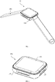
FIG. 1 illustrates a schematic view of a wearable device according to an embodiment of the present disclosure. -
FIG. 2 illustrates a schematic view of an electronic device of the wearable device ofFIG. 1 . -
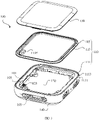
FIG. 3 illustrates a schematic exploded view of the electronic device of the wearable device ofFIG. 2 . -
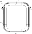
FIG. 4 illustrates a schematic top view of the electronic device of the wearable device inFIG. 2 . -
FIG. 5 illustrates a schematic cross-sectional view of the electronic device of the wearable device inFIG. 4 taken along a line A-A. -
FIG. 6 illustrates a schematic enlarged schematic view of a portion B of the electronic device of the wearable device inFIG. 5 . -
FIG. 7 illustrates a schematic view of a support of the electronic device of the wearable device ofFIG. 3 . -
FIG. 8 illustrates a schematic front view of the support of the electronic device of the wearable device ofFIG. 7 . -
FIG. 9 illustrates a schematic right view of the support of the electronic device of the wearable device ofFIG. 8 . -
FIG. 10 illustrates a schematic rear view of the support of the electronic device of the wearable device ofFIG. 8 . - In order to facilitate the understanding of the present disclosure, the present disclosure will be more fully described below with reference to relevant drawings. Even though preferred embodiments of the present disclosure are shown in the accompanying drawings, the present disclosure can be implemented in many different forms and is not limited to the embodiments described herein. These described embodiments are provided for a more thorough and comprehensive understanding of the present disclosure.
- Referring to
FIGS. 1, 2 and3 , awearable device 10 includes anelectronic device 100 and astrap 200. Thestrap 200 is mounted to theelectronic device 100 and configured to allow theelectronic device 100 to be worn to a wrist of a user. Theelectronic device 100 includes amiddle frame 110 and electronic components such as acircuit board 120 and a battery. Themiddle frame 110 is provided with amounting cavity 101. The electronic components such as thecircuit board 120 and the battery are disposed in themounting cavity 101, and thestrap 200 is connected to themiddle frame 110. In some embodiments, thewearable device 10 may be a smart watch; and theelectronic device 100 includes adisplay module 130, which covers an end of themounting cavity 101 and is connected to themiddle frame 110, and can be configured to display information and provide an interactive interface for the user. Themounting cavity 101 can be configured for mounting electronic components such as the battery, thecircuit board 120, thedisplay module 130, and a biosensor. Electronic components such as a processor, a memory unit, and a communication module can be integrated ontocircuit board 120. The battery can supply power for thecircuit board 120, thedisplay module 130 and other electronic components. Further, theelectronic device 100 may include aback cover 140, which is disposed at an end of themiddle frame 110 facing away from thedisplay module 130 and covers another end of themounting cavity 101. - Referring to
FIGS. 4 ,5 and 6 , thedisplay module 130 may further include adisplay screen 131 and acover plate 133 covering thedisplay screen 131. Thedisplay screen 131 may be a liquid crystal display (LCD) screen or an organic light-emitting diode (OLED) screen. The cover plate may be aglass cover plate 133 or asapphire cover plate 133. Thecover plate 133 is transparent and has a relatively high light transmittance, for example, the light transmittance of thecover plate 133 is above 80%. Thedisplay module 130 may have a touch function, but the touch function is not essential. The biosensor can be configured to detect biological data such as a heart rate, a respiration rate, a blood pressure, or body fat. In some embodiments, the biosensor may further configured to detect a motion state, such as for step counting. In some embodiments, thewearable device 10 may be a smart watch or a sports watch, and a common form of the sports watch is an electronic watch. In other embodiments, thewearable device 10 may be a smart bracelet, and thedisplay module 130 may be not essential. - The
middle frame 110 is a substantially rectangle. Four corners of the rectangle can be processed by a chamfering process to have circular arcs, such that thewearable device 10 has a better appearance characteristic. In other embodiments, themiddle frame 110 may be a circular frame in shape. Referring toFIGS. 2 and3 , a side of themiddle frame 110 may be provided with aslot 103 for installing thestrap 200. Referring toFIG. 1 , thestrap 200 is a belt in shape, and can be installed to themiddle frame 110 through theslot 103 and can form a reliable connection with themiddle frame 110, so as to reliably wear theelectronic device 100 to an arm of the user. In some embodiments, thestrap 200 can be easily detached from themiddle frame 110, so that thestrap 200 can be conveniently changed by the user. For example, the user can purchase various styles ofstraps 200, and change thestraps 200 according to usage scenarios to improve the convenience of use. For example, in a formal occasion, the user can use a moreformal strap 200 of thestraps 200, while in a recreational occasion, the user can use a casual typedstrap 200. In some embodiments, thestrap 200 is divided into two sections, opposite ends of theelectronic device 100 are respectively provided with theslots 103, an end of each of two sections of thestrap 200 is connected to theelectronic device 100, and ends of the two sections of thestrap 200 facing away from theelectronic device 100 can be buckled to form an accommodation space, thewearable device 10 can be worn onto the wrist of the user through thestrap 200. In other embodiments, thestrap 200 can be a one-piece structure, and two ends of thestrap 200 are each connected to theelectronic device 100. A size of the accommodation space of thestrap 200 can be adjusted by other structures, such as a snap ring, a buckle, an elastic expansion, so as to be convenient for the user to wear. - Further, referring to
FIG. 3 , themiddle frame 110 includes aframe body 111, a support113 and anantenna 115. Thesupport 113 is connected to an end of theframe body 111 and forms amounting cavity 101 with theframe body 111. Referring toFIGS. 7 and 8 , thesupport 113 is provided with amating surface 113a, and thedisplay module 130 is stacked on themating surface 113a and covers an end of themounting cavity 101. Theantenna 115 is located on thesupport 113 and exposed to themating surface 113a. Thecircuit board 120 is electrically connected to theantenna 115, and thecircuit board 120 can feed a current into theantenna 115. Theframe body 111 may be made of a non-metal material such as plastic, rubber, silica gel, wood, ceramic or glass, or may be made of a metal material such as stainless steel, aluminum alloy or magnesium alloy. Further, theframe body 111 may be a metal injection molded part, that is, a structural rigidity of theframe body 111 is ensured by using a metal material thereof, and an inner surface of theframe body 111 is formed with structures for assembly and positioning such as protrusions, grooves, screw holes by injection molding. It can be understood that the mountingcavity 101 can also be separately formed by theframe body 111, and thesupport 113 is not essential, and theantenna 115 can be directly located onto theframe body 111. A material of theback cover 140 may be the same as that of theframe body 111, or may be different from that of theframe body 111. For example, theback cover 140 can be made of a non-metal material such as glass, ceramic or plastic, or theback cover 140 can also be made of a metal material such as stainless steel or aluminum alloy. - In some embodiments, the
support 113 may be made of a laser direct structuring (LDS) plastic. Anantenna receiving slot 113b and theantenna 115 are carved by laser on themating surface 113a of thesupport 113, and theantenna 115 is accommodated in and extends along theantenna receiving slot 113b. Specifically, a LDS material contains a metal component and a non-metal component such as a plastic. During the laser carving process, the non-metal component such as the plastic is dissolved and evaporated to form theantenna receiving slot 113b, and the metal component of the LDS material is precipitated and deposited in theantenna receiving slot 113b to form theantenna 115. Since the non-metal material is removed, on a side of themetal antenna 115 facing towards thedisplay module 130, themating surface 113a is protruded with respect to theantenna 115 or flush with theantenna 115. In other words, a height difference exists between the side of theantenna 115 facing towards thedisplay module 130 and themating surface 113a, or the side of theantenna 115 facing towards thedisplay module 130 is flush with themating surface 113a. - In other embodiments, the
support 113 may be made of other non-metal material such as silica gel or an ordinary plastic. Thesupport 113 has themating surface 113a, themating surface 113a can be provided with theantenna receiving slot 113b, and then theantenna 115 is located in theantenna receiving slot 113b, such that themating surface 113a protrudes from the antenna or is flush with theantenna 115. Theantenna 115 with this structure can reduce an overall thickness of theelectronic device 100, which is beneficial to the thin and light design of theelectronic device 100. - During an assembly process of the
electronic device 100, themating surface 113a can be formed with an adhesive layer by a dispensing process to reliably connect thedisplay module 130 to thesupport 113. Compared with the antenna in the form of flexible circuit board, theantenna 115 with the above structure does not increase the overall thickness of theelectronic device 100, so it is beneficial to the thin and light design of theelectronic device 100, and further beneficial to the thin and light design of the wearable device. - With respect to the
electronic device 100, theantenna 115 is exposed to themating surface 113a of themiddle frame 110, and thedisplay module 130 is stacked on themating surface 113a and covers theantenna 115 and the mountingcavity 101, as such, compared with the antenna in the form of the flexible circuit board, theabove antenna 115 can reduce the overall thickness of theelectronic device 100. For example, the thickness of theantenna 115 in the form of the flexible circuit board is usually about 0.25 millimeters (mm). Compared with the antenna in the form of flexible circuit board, the overall thickness of theelectronic device 100 of the present disclosure can be reduced by 0.25 mm, which is beneficial to the thin and light design of theelectronic device 100. - Since the
antenna 115 is formed on thesupport 113, a distance between theantenna 115 and an outer surface of thedisplay module 130 is relatively small after themating surface 113a is connected to thedisplay module 130. Taking theantenna 115 as a near field communication (NFC ) antenna of theelectronic device 100 as an example, when the outer surfaces of the display modules of the present disclosure and the related art are at the same distance from radio frequency identification (RFID) readers and other devices, theantenna 115 of the present disclosure can transmit and receive relatively strong signals, and can improve an anti-interference and anti-shielding performance of theantenna 115, so as to improve a communication performance of theelectronic device 100. Further, in other embodiments, theantenna 115 can be another typed antenna, such as an antenna for transmitting and receiving cellular signals, and theantenna 115 with the above structure can also improve the communication performance of theelectronic device 100. - Further, referring to
FIGS. 7 and 8 , thesupport 113 is defined with agroove opening 113c of the mountingcavity 101. In an embodiment of the present invention, a cross section of thegroove opening 113c is substantially a rounded rectangle, that is, four corners of the rectangle are formed by arc transition. Thesupport 113 is enclosed in a circumferential direction of thegroove opening 113c, and themating surface 113a and theantenna receiving slot 113b extend in the circumferential direction of thegroove opening 113c. Further, in some embodiments, thesupport 113 includes a supportingportion 1131 and a limitingportion 1133 which are integrally formed, and themating surface 113a and thegroove opening 113c are located on the supportingportion 1131, so that a cross section of thesupport 113 is substantially L-shaped. On a side of themating surface 113a facing towards thedisplay module 130, the limitingportion 1133 protrudes from the supportingportion 1131 and extends along an edge of the supportingportion 1131 to form a circumferentially enclosed structure. Further, referring toFIG. 6 , the limitingportion 1133 is arranged surrounding thedisplay module 130. The arrangement of the limitingportion 1133 facilitates the assembly and positioning of thedisplay module 130 on thesupport 113. For example, after the adhesive layer is formed on themating surface 113a, thedisplay module 130 is installed onto thesupport 113, such that the limitingportion 1133 can limit an edge of thedisplay module 130, and can improve a sealing performance between thedisplay module 130 and thesupport 113, thereby improving a waterproof and dustproof performance of theelectronic device 100. In the embodiment where the mountingcavity 101 is defined by theframe body 111, thegroove opening 113c of thesupport 113 may connect to the mountingcavity 101. - Referring to
FIGS. 7 ,9 and10 , in some embodiments, thesupport 113 includes a connectingportion 1135 integrally formed with the supportingportion 1131, and the connectingportion 1135 is protruded into the mountingcavity 101. Further, the connectingportion 1135 is arranged to be protruded from a side wall of thegroove opening 113c. A side of the connectingportion 1135 facing away from thedisplay module 130 is provided with afeeding point 1151. Thefeeding point 1151 is electrically connected to thecircuit board 120 and configured for feeding a current into theantenna 115. In some embodiments, the connectingportion 1135 and thesupport 113 are made of the same material, a LDS plastic. The supportingportion 1131 and the connectingportion 1135 are formed with a connectingwire 1153, which connects thefeeding point 1151 and theantenna 115. Thefeeding point 1151 and the connectingwire 1153 are both formed by the laser carving process, thus simplifying the process of thefeeding point 1151 and the connectingwire 1153. Further, referring toFIGS. 7 and10 , the connectingportion 1135 includes afirst surface 1135a, asecond surface 1135b, and anend surface 1135c connected between thefirst surface 1135a and thesecond surface 1135b. Thefirst surface 1135a faces towards thedisplay module 130, the feeding points 1151 are exposed to thesecond surface 1135b, and the connectingwire 1153 extends along thefirst surface 1135a and theend surface 1135c to thesecond surface 1135b and is configured to conduct the feeding points 1151 with theantenna 115. Further, in some embodiments, a height difference exists between thefirst surface 1135a and themating surface 113a, which can be used to avoid contact between the limiting portion and thedisplay screen 131, so as to reduce the overall thickness of theelectronic device 100. - Further, referring to
FIG. 6 , thecircuit board 120 includes aboard body 121 and aresilient component 123 for example, a resilient sheet, disposed on theboard body 121. Theresilient component 123 protrudes from a side of theboard body 121 facing towards thedisplay module 130, and the connectingportion 1135 presses against theresilient component 123, and thefeeding point 1151 conducts with theresilient component 123. The arrangement of theresilient component 123 can keep the reliability of the electrical connection between thefeeding point 1151 and thecircuit board 120, thus ensuring a communication performance of theelectronic device 100. - Referring to
FIG. 3 , in some embodiments, theboard body 121 is connected to theframe body 111 with a threaded fastener such as a screw, and theresilient component 123 is two in number, and the tworesilient component 123 are arranged at intervals on a side of theboard body 121 facing towards thedisplay module 130 and arranged at an edge of theboard body 121. Thefeeding point 1151 is two in number, and the twofeeding points 1151 are spaced apart and correspond to the tworesilient component 123 by one-to-one correspondence. After theelectronic device 100 is assembled and molded, the connectingportion 1135 covers theresilient component 123, and the feeding points 1151 press theresilient components 123 and conduct with theresilient components 123, so that the current of thecircuit board 120 can be fed into theantenna 115. - In some embodiments, the
antenna 115 is generally annular and distributed on a circumferential edge of thedisplay module 130. Furthermore, after thedisplay module 130 is assembled with thesupport 113, an edge of thecover plate 133 of thedisplay module 130 is stacked with themating surface 113a, and thecover plate 133 covers theantenna 115. Thedisplay screen 131 of thedisplay module 130 is not stacked with themating surface 113a, thus preventing thedisplay screen 131 from increasing the overall thickness of theelectronic device 100 and weakening a shielding effect of thedisplay screen 131 on theantenna 115. Specifically, referring toFIG. 6 , a marginal region A1 is formed between a circumferential edge of thedisplay screen 131 and a circumferential edge of thecover plate 133, and the marginal region A1 covers theantenna 115. In other words, taking a geometric plane perpendicular to a thickness direction of theelectronic device 100 as a reference plane, an orthogonal projection of theantenna 115 on the reference plane is located outside of an orthogonal projection of thedisplay screen 131 on the reference plane, that is, the orthogonal projection of theantenna 115 on the reference plane does not overlap with the orthogonal projection of thedisplay screen 131 on the reference plane, that is, thedisplay screen 131 does not cover theantenna 115 in the thickness direction of theelectronic device 100. - In the above embodiment, since the
display screen 131 does not cover theantenna 115 in the thickness direction of theelectronic device 100, there is a relatively small distance between theantenna 115 and an outer surface of thecover plate 133, so that a strength of a signal received or transmitted by theantenna 115 can be improved, and the communication performance of theelectronic device 100 can be improved. Taking theantenna 115 as the NFC antenna of theelectronic device 100 as an example, when the outer surfaces of the cover plates of the present disclosure and the related art are at the same distance from RFID readers and other devices, theantenna 115 of the present disclosure can transmit and receive relatively strong signals, and can improve the anti-interference and anti-shielding performance of theantenna 115, so as to enhance the communication performance of theelectronic device 100. - Further, in other embodiments, in the thickness direction of the
electronic device 100, thedisplay screen 131 may cover part or all of theantenna 115, however, since themating surface 113a protrudes from theantenna 115 or is flush with the side of theantenna 115 facing towards thedisplay screen module 130, the arrangement of theantenna 115 can also reduce the overall thickness of theelectronic device 100, which is beneficial to the thin and light design of theelectronic device 100. - Referring to
FIG. 9 , in some embodiments, on a side of the supportingportion 1131 facing away from themating surface 113a, the connectingportion 1135 protrudes relative to the supportingportion 1131. This structural arrangement of the connectingportion 1135 can be configured for the assembly and positioning of thesupport 113. For example, one of a side of the connectingportion 1135 facing away from theend surface 1135c and a side of theframe body 111 facing towards the connectingportion 1135 may be provided with a groove, and the other of the side of the connectingportion 1135 facing away from theend surface 1135c and the side of theframe body 111 facing towards the connectingportion 1135 may be provided with a protrusion, so that after thesupport 113 is assembled in theframe body 111, the groove and the protrusion can be engaged with one another, thereby improving connection reliability of thesupport 113 and theframe body 111. Referring toFIG. 3 , for another example, theframe body 111 is provided with apositioning groove 105, the connectingportion 1135 is accommodated in thepositioning groove 105, after thesupport 113 is assembled in theframe body 111, and thepositioning groove 105 can limit the movement of the connectingportion 1135, thus bringing out a reliable limiting effect on the connectingportion 1135. - Further, it is not essential that the connecting
portion 1135 protrudes from the side of the supportingportion 1131 facing away from themating surface 113a. For example, the connectingportion 1135 can be omitted, and theantenna 115 can be extended to the side of the supportingportion 1131 facing away from themating surface 113a by the laser carving process, and then can be electrically connected to thecircuit board 120 to feed a current into theantenna 115. For another example, the connectingportion 1135 can be an independent part and fixed to thesupport 113 by welding, bonding or screwing, and then theantenna 115 is electrically connected to thecircuit board 120 through the connectingportion 1135. - Further, referring to
FIG. 6 andFIG. 3 , theframe body 111 includes an abuttingportion 1111 and a stoppingportion 1113 connected to the abuttingportion 1111. For example, the abuttingportion 1111 and the stoppingportion 1113 can be integrally formed. The abuttingportion 1111 extends along a circumferential direction of the mountingcavity 101 and is configured to support thesupport 113. The stoppingportion 1113 protrudes from a side of the abuttingportion 1111 facing towards thedisplay screen module 130 and extends along an edge of the abuttingportion 1111 to form a circumferentially enclosed structure. Thesupport 113 is connected to the abuttingportion 1111 and the stoppingportion 1113 is arranged surrounding thesupport 113. In other words, in an embodiment of the present invention, a part of theframe body 111 for assembling with thesupport 113 is stepped, thesupport 113 is arranged at the step and thesupport 113 is surrounded by the stoppingportion 1113. The arrangement of the stoppingportion 1113 facilitates the assembly and positioning of thesupport 113 onto theframe body 111. For example, the abuttingportion 1111 may be provided with an adhesive layer, and thesupport 113 can be fixedly connected to theframe body 111 through the adhesive layer, so that theframe body 111 can limit an edge of thesupport 113, thereby improving a sealing performance between thesupport 113 and theframe body 111, and further improving a waterproof and dustproof performance of theelectronic device 100. - Further, referring to
FIG. 6 , on a side of theframe body 111 facing towards thedisplay module 130, a tail end of the limitingportion 1133 is protruded with respect to the stoppingportion 1113, or the tail end of the limitingportion 1133 is flush with the stoppingportion 1113. Furthermore, end surfaces of the limitingportion 1133 and the stoppingportion 1113 can be treated with to form curved surfaces, so that the end surfaces of the limitingportion 1133 and the stoppingportion 1113 and a surface of thecover plate 133 form a continuous curved profile, thereby improving an appearance characteristic of theelectronic device 100. - Technical features of the above-mentioned embodiments can be arbitrarily combined. To make the description concise, all possible combinations of the technical features in the above-mentioned embodiments are not described. However, as long as there is no contradiction in the combination of these technical features, it should be considered as to be fall with the scope of this specification.
- The above-mentioned embodiments are merely several embodiments of the present invention, and descriptions thereof are more specific and detailed, but they should not be construed as limiting the scope of protection of the present disclose. It should be pointed out that, for those skilled in the art, without departing from the concept of the present disclosure, several modifications and improvements can be made, all of which belong to the scope of protection of the present disclosure. Therefore, the scope of protection of the present disclosure should be subject to the appended claims.
Claims (31)
- An electronic device, comprising:a cover plate;a middle frame, provided with a mounting cavity and a mating surface, wherein the middle frame comprises an antenna exposed from the mating surface, the cover plate is stacked on the mating surface and covers the antenna and the mounting cavity; anda circuit board, arranged in the mounting cavity and electrically connected to the antenna.
- The electronic device according to claim 1, wherein the middle frame comprises a frame body and a support, the support is connected to an end of the frame body and forms the mounting cavity together with the frame body, the mating surface is located on the support, and the antenna is arranged on the support.
- The electronic device according to claim 2, further comprising a display screen, wherein the display screen is electrically connected to the circuit board, and the cover plate covers the display screen.
- The electronic device according to claim 3, wherein a marginal region is formed between a circumferential edge of the display screen and a circumferential edge of the cover plate, and the marginal region covers the antenna.
- The electronic device according to claim 2, wherein an antenna receiving slot is formed at a side of the support at which the mating surface is located, and the antenna is accommodated in and extends along the antenna receiving slot.
- The electronic device according to claim 5, wherein the support is made of a laser direct structuring (LDS) plastic.
- The electronic device according to claim 6, wherein the antenna receiving slot and the antenna are carved by laser on the support.
- The electronic device according to claim 6, wherein the mating surface is protruded relative to the antenna, or flush with a side of the antenna facing towards the cover plate.
- The electronic device according to claim 6, wherein the support is defined with a groove opening of the mounting cavity, the support is closed in a circumferential direction of the groove opening, and the mating surface and the antenna receiving slot extend in the circumferential direction of the groove opening.
- The electronic device according to claim 9, wherein the support comprises a supporting portion and a limiting portion which are integrally formed, the mating surface and the groove opening are located on the supporting portion; on a side of the mating surface facing towards the cover plate, the limiting portion protrudes from the supporting portion and extends along an edge of the supporting portion to form a circumferentially enclosed structure; and the limiting portion is arranged surrounding the cover plate.
- The electronic device according to claim 10, wherein the frame body comprises an abutting portion and a stopping portion connected to the abutting portion, the abutting portion extends along a circumferential direction of the mounting cavity, the stopping portion protrudes from a side of the abutting portion facing towards the cover plate and extends along the abutting portion to form a circumferentially enclosed structure, the support is connected to the abutting portion, and the stopping portion is arranged surrounding the support.
- The electronic device according to claim 11, wherein on a side of the frame body facing towards the cover plate, a tail end of the limiting portion is protruded with respect to the stopping portion or the tail end of the limiting portion is flush with the stopping portion.
- The electronic device according to claim 10, wherein the support comprises a connecting portion integrally formed with the supporting portion, the connecting portion is protruded into the mounting cavity, a side of the connecting portion facing away from the cover plate is provided with a feeding point, and the feeding point is electrically connected to the circuit board and configured for feeding a current into the antenna.
- The electronic device according to claim 13, wherein the connecting portion comprises a first surface, a second surface opposite to the first surface, and an end surface connected between the first surface and the second surface; the first surface faces towards the cover plate, the feeding point is exposed from the second surface, the support is provided with a connecting wire, and the connecting wire extends along the first surface and the end surface to the second surface and is configured to conduct the feeding point with the antenna.
- The electronic device according to claim 13, wherein on a side of the supporting portion facing away from the mating surface, the connecting portion protrudes relative to the supporting portion.
- The electronic device according to claim 13, wherein the circuit board comprises a board body and a resilient component disposed on the board body, the resilient component protrudes from a side of the board body facing towards the cover plate, and the connecting portion presses against the resilient component and conducts with the resilient component.
- An electronic device, comprising:a display module;a middle frame, comprising a frame body and a support, wherein the frame body is provided with a mounting cavity, the support is connected to an end of the frame body and has a mating surface, the display module is stacked on the mating surface and covers the mounting cavity, the support comprises an antenna exposed from the mating surface, and the mating surface is protruded with respect to the antenna or flush with a side of the antenna facing towards the display module; anda circuit board, arranged in the mounting cavity and electrically connected to the antenna.
- The electronic device according to claim 17, wherein the support is made of a LDS plastic, and the antenna are carved by laser on the support.
- The electronic device according to claim 17, wherein the support is provided with a groove opening communicated with the mounting cavity, and the mating surface extends in a circumferential direction of the groove opening to form a closed shape.
- The electronic device according to claim 19, wherein the support comprises an one-piece structure of a supporting portion and a limiting portion, the mating surface and the groove opening are located on the supporting portion; on a side of the mating surface facing towards the display module, the limiting portion protrudes from the supporting portion and extends along an edge of the supporting portion to form a circumferentially enclosed structure; and the limiting portion is arranged surrounding the display module.
- The electronic device according to claim 20, wherein the frame body comprises an abutting portion and a stopping portion connected to the abutting portion, the abutting portion extends along a circumferential direction of the mounting cavity, the stopping portion protrudes from a side of the abutting portion facing towards the display module and extends along the abutting portion to form a circumferentially enclosed structure, the support is connected to the abutting portion, and the stopping portion is arranged surrounding the support.
- The electronic device according to claim 20, wherein the support comprises a connecting portion integrally formed with the supporting portion, the connecting portion is protruded from a side wall of the groove opening, a side of the connecting portion facing away from the display module is provided with a feeding point, and the feeding point are contacted and electrically conducted with the circuit board and configured to feed a current into the antenna.
- The electronic device according to claim 22, wherein the connecting portion comprises a first surface and a second surface opposite to the first surface, the first surface faces towards the display module and forms a height difference with the mating surface, the feeding point is exposed from the second surface, the support is provided with a connecting wire, and the connecting wire extends along the first surface to the second surface and is configured to electrically conduct the feeding point with the antenna.
- The electronic device according to claim 22, wherein on a side of the supporting portion facing away from the display module, the connecting portion protrudes from the supporting portion; the frame body is provided with a positioning groove, and the connecting portion is accommodated in the positioning groove.
- The electronic device according to any one of claims 17 to 24, wherein the display module comprises a cover plate and a display screen, the cover plate is transparent and covers the display screen, and the cover plate is connected to the mating surface and covers the antenna.
- The electronic device according to claim 25, wherein an orthogonal projection of the antenna on a reference plane is located outside of an orthogonal projection of the display screen on the reference plane, and the reference plane is a geometric plane perpendicular to a thickness direction of the electronic device.
- An electronic device, comprising:a middle frame, provided with a mounting cavity, wherein the middle frame has a mating surface at an end of the mounting cavity, and the mating surface extends around the mounting cavity;an antenna, arranged on the mating surface and extending around the mounting cavity; anda cover plate, stacked on the mating surface and covering the antenna and the mounting cavity.
- The electronic device according to claim 27, wherein at least part of the middle frame is made of a LDS plastic, and the antenna is carved by laser on the LDS plastic.
- The electronic device according to claim 28, wherein the mating surface is protruded relative to the antenna or flush with a side of the antenna facing towards the cover plate.
- The electronic device according to claim 29, wherein the middle frame comprises a supporting portion and a limiting portion integrally formed, the supporting portion has the mating surface, and the limiting portion extends around the mounting cavity; and on a side of the mating surface facing towards the cover plate, the limiting portion protrudes from the supporting portion and is arranged surrounding the cover plate.
- A wearable device, comprising:a strap; andthe electronic device according to any one of claims 1 to 30,wherein the strap is connected to the middle frame and configured to allow the electronic device to be worn onto a wrist of a user.
Applications Claiming Priority (2)
| Application Number | Priority Date | Filing Date | Title |
|---|---|---|---|
| CN202010258378.7A CN113497331B (en) | 2020-04-03 | 2020-04-03 | Electronics and Wearables |
| PCT/CN2021/075014 WO2021196878A1 (en) | 2020-04-03 | 2021-02-03 | Electronic device and wearable device |
Publications (2)
| Publication Number | Publication Date |
|---|---|
| EP4109677A1 true EP4109677A1 (en) | 2022-12-28 |
| EP4109677A4 EP4109677A4 (en) | 2023-08-23 |
Family
ID=77927697
Family Applications (1)
| Application Number | Title | Priority Date | Filing Date |
|---|---|---|---|
| EP21780108.3A Withdrawn EP4109677A4 (en) | 2020-04-03 | 2021-02-03 | ELECTRONIC DEVICE AND PORTABLE DEVICE |
Country Status (4)
| Country | Link |
|---|---|
| US (1) | US20230006338A1 (en) |
| EP (1) | EP4109677A4 (en) |
| CN (1) | CN113497331B (en) |
| WO (1) | WO2021196878A1 (en) |
Families Citing this family (6)
| Publication number | Priority date | Publication date | Assignee | Title |
|---|---|---|---|---|
| US20230122975A1 (en) * | 2021-10-15 | 2023-04-20 | Apple Inc. | Integrated multipart housing for an electronic device |
| CN217768748U (en) * | 2022-04-19 | 2022-11-08 | 华为技术有限公司 | Electronic equipment and electronic equipment assembly |
| CN220192374U (en) * | 2022-11-28 | 2023-12-19 | 北京心有灵犀科技有限公司 | NFC ornaments |
| CN115986369B (en) * | 2023-01-04 | 2025-11-11 | 歌尔股份有限公司 | Display screen module and wearable equipment |
| CN118642345A (en) * | 2023-03-13 | 2024-09-13 | 华为终端有限公司 | Electronic devices |
| CN120276231A (en) * | 2023-12-29 | 2025-07-08 | 荣耀终端股份有限公司 | Wearing equipment |
Family Cites Families (17)
| Publication number | Priority date | Publication date | Assignee | Title |
|---|---|---|---|---|
| EP0741433B1 (en) * | 1995-05-05 | 2001-10-04 | Eta SA Fabriques d'Ebauches | Antenna structure for use in a timepiece |
| JP4649879B2 (en) * | 2004-06-07 | 2011-03-16 | カシオ計算機株式会社 | Wireless module and electronic device |
| JP5938952B2 (en) * | 2012-03-02 | 2016-06-22 | セイコーエプソン株式会社 | Electronic clock with built-in antenna |
| US9979078B2 (en) * | 2012-10-25 | 2018-05-22 | Pulse Finland Oy | Modular cell antenna apparatus and methods |
| KR102163406B1 (en) * | 2014-02-21 | 2020-10-08 | 삼성전자주식회사 | Electronic device and fabricating method for housing of the same |
| TWM507000U (en) * | 2015-06-10 | 2015-08-11 | 廣達電腦股份有限公司 | Wearable electronic device |
| US9653786B2 (en) * | 2015-06-27 | 2017-05-16 | Intel Corporation | Wearable antenna system |
| CN105206918A (en) * | 2015-08-28 | 2015-12-30 | 宇龙计算机通信科技(深圳)有限公司 | Antenna device of mobile terminal and mobile terminal |
| CN105573111A (en) * | 2016-02-17 | 2016-05-11 | 广东小天才科技有限公司 | Intelligent wearable device |
| CN107293849B (en) * | 2016-03-31 | 2020-01-10 | 宇龙计算机通信科技(深圳)有限公司 | NFC antenna structure and mobile terminal |
| CN105870580A (en) * | 2016-04-06 | 2016-08-17 | 成都天奥电子股份有限公司 | Watch antenna and watch equipped with same |
| WO2018168852A1 (en) * | 2017-03-14 | 2018-09-20 | シチズン時計株式会社 | Radio clock |
| CN107689483A (en) * | 2017-08-09 | 2018-02-13 | 捷开通讯(深圳)有限公司 | Antenna module and electronic equipment |
| CN108336475B (en) * | 2018-01-29 | 2020-01-17 | Oppo广东移动通信有限公司 | A middle frame assembly, electronic equipment and assembling method thereof |
| US10476170B2 (en) * | 2018-02-27 | 2019-11-12 | Apple Inc. | Antenna arrays having conductive shielding buckets |
| CN208127422U (en) * | 2018-03-30 | 2018-11-20 | 广东欧珀移动通信有限公司 | Antenna assembly and electronic equipment |
| US12095148B2 (en) * | 2019-10-10 | 2024-09-17 | Google Llc | Water seal design with antenna co-existence on electronic device |
-
2020
- 2020-04-03 CN CN202010258378.7A patent/CN113497331B/en active Active
-
2021
- 2021-02-03 WO PCT/CN2021/075014 patent/WO2021196878A1/en not_active Ceased
- 2021-02-03 EP EP21780108.3A patent/EP4109677A4/en not_active Withdrawn
-
2022
- 2022-09-06 US US17/929,953 patent/US20230006338A1/en not_active Abandoned
Also Published As
| Publication number | Publication date |
|---|---|
| CN113497331B (en) | 2023-03-10 |
| CN113497331A (en) | 2021-10-12 |
| EP4109677A4 (en) | 2023-08-23 |
| WO2021196878A1 (en) | 2021-10-07 |
| US20230006338A1 (en) | 2023-01-05 |
Similar Documents
| Publication | Publication Date | Title |
|---|---|---|
| US20230006338A1 (en) | Electronic device and wearable device | |
| US11747662B2 (en) | Electronic device and wearable device with elastomeric member | |
| US9256250B2 (en) | Electronic devices with flexible displays having fastened bent edges | |
| KR102044505B1 (en) | Housing, manufacturing method thereof and electronic device using same | |
| US20160261032A1 (en) | Wearable electronic device | |
| US9331733B2 (en) | Wireless communication terminal device | |
| CN107623173A (en) | Functional components and mobile terminals | |
| EP3799200B1 (en) | Antenna clip and electronic device comprising same | |
| CN112602309A (en) | Camera support, camera assembly and terminal | |
| WO2021169702A1 (en) | Shell assembly, electronic device and wearable device | |
| US20160323004A1 (en) | Protective cover and electronic device having it | |
| CN212846392U (en) | Case components, electronic devices and wearable devices | |
| US12381309B2 (en) | Antenna mounted on wearable device | |
| US11262710B2 (en) | Timepiece with physical authentication mark | |
| CN110519432B (en) | Electronic device | |
| US11360435B2 (en) | Electronic apparatus | |
| CN111834149B (en) | Key module and electronic device | |
| WO2021169701A1 (en) | Electronic apparatus and wearable apparatus | |
| CN217695464U (en) | Watchband device and intelligent watch | |
| CN215955140U (en) | Key structure and electronic equipment | |
| US11144015B2 (en) | Antenna device and timepiece | |
| CN109157759B (en) | Wrist strap type laser therapeutic apparatus | |
| CN113311687B (en) | Shell assembly, electronic equipment and wearable equipment | |
| CN224083657U (en) | Bluetooth antenna and over-ear Bluetooth headphones | |
| CN215183601U (en) | Switch components and mobile terminals |
Legal Events
| Date | Code | Title | Description |
|---|---|---|---|
| STAA | Information on the status of an ep patent application or granted ep patent |
Free format text: STATUS: THE INTERNATIONAL PUBLICATION HAS BEEN MADE |
|
| PUAI | Public reference made under article 153(3) epc to a published international application that has entered the european phase |
Free format text: ORIGINAL CODE: 0009012 |
|
| STAA | Information on the status of an ep patent application or granted ep patent |
Free format text: STATUS: REQUEST FOR EXAMINATION WAS MADE |
|
| 17P | Request for examination filed |
Effective date: 20220921 |
|
| AK | Designated contracting states |
Kind code of ref document: A1 Designated state(s): AL AT BE BG CH CY CZ DE DK EE ES FI FR GB GR HR HU IE IS IT LI LT LU LV MC MK MT NL NO PL PT RO RS SE SI SK SM TR |
|
| DAV | Request for validation of the european patent (deleted) | ||
| DAX | Request for extension of the european patent (deleted) | ||
| REG | Reference to a national code |
Ref country code: DE Ref legal event code: R079 Free format text: PREVIOUS MAIN CLASS: H01Q0001380000 Ipc: G04G0021040000 |
|
| A4 | Supplementary search report drawn up and despatched |
Effective date: 20230725 |
|
| RIC1 | Information provided on ipc code assigned before grant |
Ipc: H01Q 1/38 20060101ALI20230719BHEP Ipc: H01Q 1/24 20060101ALI20230719BHEP Ipc: H01Q 1/27 20060101ALI20230719BHEP Ipc: G04R 60/06 20130101ALI20230719BHEP Ipc: G04G 21/04 20130101AFI20230719BHEP |
|
| STAA | Information on the status of an ep patent application or granted ep patent |
Free format text: STATUS: THE APPLICATION HAS BEEN WITHDRAWN |
|
| 18W | Application withdrawn |
Effective date: 20240112 |