EP4109519A2 - Semiconductor package with releasable isolation layer protection - Google Patents
Semiconductor package with releasable isolation layer protection Download PDFInfo
- Publication number
- EP4109519A2 EP4109519A2 EP22179091.8A EP22179091A EP4109519A2 EP 4109519 A2 EP4109519 A2 EP 4109519A2 EP 22179091 A EP22179091 A EP 22179091A EP 4109519 A2 EP4109519 A2 EP 4109519A2
- Authority
- EP
- European Patent Office
- Prior art keywords
- isolation structure
- releasable
- semiconductor
- package body
- package
- Prior art date
- Legal status (The legal status is an assumption and is not a legal conclusion. Google has not performed a legal analysis and makes no representation as to the accuracy of the status listed.)
- Pending
Links
Images



Classifications
-
- H—ELECTRICITY
- H10—SEMICONDUCTOR DEVICES; ELECTRIC SOLID-STATE DEVICES NOT OTHERWISE PROVIDED FOR
- H10W—GENERIC PACKAGES, INTERCONNECTIONS, CONNECTORS OR OTHER CONSTRUCTIONAL DETAILS OF DEVICES COVERED BY CLASS H10
- H10W40/00—Arrangements for thermal protection or thermal control
- H10W40/70—Fillings or auxiliary members in containers or in encapsulations for thermal protection or control
- H10W40/77—Auxiliary members characterised by their shape
- H10W40/778—Auxiliary members characterised by their shape in encapsulations
-
- H—ELECTRICITY
- H10—SEMICONDUCTOR DEVICES; ELECTRIC SOLID-STATE DEVICES NOT OTHERWISE PROVIDED FOR
- H10W—GENERIC PACKAGES, INTERCONNECTIONS, CONNECTORS OR OTHER CONSTRUCTIONAL DETAILS OF DEVICES COVERED BY CLASS H10
- H10W74/00—Encapsulations, e.g. protective coatings
- H10W74/10—Encapsulations, e.g. protective coatings characterised by their shape or disposition
- H10W74/111—Encapsulations, e.g. protective coatings characterised by their shape or disposition the semiconductor body being completely enclosed
- H10W74/129—Encapsulations, e.g. protective coatings characterised by their shape or disposition the semiconductor body being completely enclosed forming a chip-scale package [CSP]
-
- H—ELECTRICITY
- H10—SEMICONDUCTOR DEVICES; ELECTRIC SOLID-STATE DEVICES NOT OTHERWISE PROVIDED FOR
- H10W—GENERIC PACKAGES, INTERCONNECTIONS, CONNECTORS OR OTHER CONSTRUCTIONAL DETAILS OF DEVICES COVERED BY CLASS H10
- H10W40/00—Arrangements for thermal protection or thermal control
- H10W40/20—Arrangements for cooling
- H10W40/25—Arrangements for cooling characterised by their materials
- H10W40/255—Arrangements for cooling characterised by their materials having a laminate or multilayered structure, e.g. direct bond copper [DBC] ceramic substrates
-
- H—ELECTRICITY
- H10—SEMICONDUCTOR DEVICES; ELECTRIC SOLID-STATE DEVICES NOT OTHERWISE PROVIDED FOR
- H10W—GENERIC PACKAGES, INTERCONNECTIONS, CONNECTORS OR OTHER CONSTRUCTIONAL DETAILS OF DEVICES COVERED BY CLASS H10
- H10W42/00—Arrangements for protection of devices
- H10W42/121—Arrangements for protection of devices protecting against mechanical damage
-
- H—ELECTRICITY
- H10—SEMICONDUCTOR DEVICES; ELECTRIC SOLID-STATE DEVICES NOT OTHERWISE PROVIDED FOR
- H10W—GENERIC PACKAGES, INTERCONNECTIONS, CONNECTORS OR OTHER CONSTRUCTIONAL DETAILS OF DEVICES COVERED BY CLASS H10
- H10W70/00—Package substrates; Interposers; Redistribution layers [RDL]
- H10W70/40—Leadframes
- H10W70/411—Chip-supporting parts, e.g. die pads
-
- H—ELECTRICITY
- H10—SEMICONDUCTOR DEVICES; ELECTRIC SOLID-STATE DEVICES NOT OTHERWISE PROVIDED FOR
- H10W—GENERIC PACKAGES, INTERCONNECTIONS, CONNECTORS OR OTHER CONSTRUCTIONAL DETAILS OF DEVICES COVERED BY CLASS H10
- H10W70/00—Package substrates; Interposers; Redistribution layers [RDL]
- H10W70/40—Leadframes
- H10W70/481—Leadframes for devices being provided for in groups H10D8/00 - H10D48/00
-
- H—ELECTRICITY
- H10—SEMICONDUCTOR DEVICES; ELECTRIC SOLID-STATE DEVICES NOT OTHERWISE PROVIDED FOR
- H10W—GENERIC PACKAGES, INTERCONNECTIONS, CONNECTORS OR OTHER CONSTRUCTIONAL DETAILS OF DEVICES COVERED BY CLASS H10
- H10W74/00—Encapsulations, e.g. protective coatings
- H10W74/01—Manufacture or treatment
-
- H—ELECTRICITY
- H10—SEMICONDUCTOR DEVICES; ELECTRIC SOLID-STATE DEVICES NOT OTHERWISE PROVIDED FOR
- H10W—GENERIC PACKAGES, INTERCONNECTIONS, CONNECTORS OR OTHER CONSTRUCTIONAL DETAILS OF DEVICES COVERED BY CLASS H10
- H10W74/00—Encapsulations, e.g. protective coatings
- H10W74/01—Manufacture or treatment
- H10W74/014—Manufacture or treatment using batch processing
-
- H—ELECTRICITY
- H10—SEMICONDUCTOR DEVICES; ELECTRIC SOLID-STATE DEVICES NOT OTHERWISE PROVIDED FOR
- H10W—GENERIC PACKAGES, INTERCONNECTIONS, CONNECTORS OR OTHER CONSTRUCTIONAL DETAILS OF DEVICES COVERED BY CLASS H10
- H10W74/00—Encapsulations, e.g. protective coatings
- H10W74/01—Manufacture or treatment
- H10W74/016—Manufacture or treatment using moulds
-
- H—ELECTRICITY
- H10—SEMICONDUCTOR DEVICES; ELECTRIC SOLID-STATE DEVICES NOT OTHERWISE PROVIDED FOR
- H10W—GENERIC PACKAGES, INTERCONNECTIONS, CONNECTORS OR OTHER CONSTRUCTIONAL DETAILS OF DEVICES COVERED BY CLASS H10
- H10W74/00—Encapsulations, e.g. protective coatings
- H10W74/10—Encapsulations, e.g. protective coatings characterised by their shape or disposition
- H10W74/111—Encapsulations, e.g. protective coatings characterised by their shape or disposition the semiconductor body being completely enclosed
- H10W74/121—Encapsulations, e.g. protective coatings characterised by their shape or disposition the semiconductor body being completely enclosed by multiple encapsulations, e.g. by a thin protective coating and a thick encapsulation
-
- H—ELECTRICITY
- H10—SEMICONDUCTOR DEVICES; ELECTRIC SOLID-STATE DEVICES NOT OTHERWISE PROVIDED FOR
- H10W—GENERIC PACKAGES, INTERCONNECTIONS, CONNECTORS OR OTHER CONSTRUCTIONAL DETAILS OF DEVICES COVERED BY CLASS H10
- H10W74/00—Encapsulations, e.g. protective coatings
- H10W74/10—Encapsulations, e.g. protective coatings characterised by their shape or disposition
- H10W74/111—Encapsulations, e.g. protective coatings characterised by their shape or disposition the semiconductor body being completely enclosed
- H10W74/124—Encapsulations, e.g. protective coatings characterised by their shape or disposition the semiconductor body being completely enclosed the encapsulations having cavities other than that occupied by chips
-
- H—ELECTRICITY
- H10—SEMICONDUCTOR DEVICES; ELECTRIC SOLID-STATE DEVICES NOT OTHERWISE PROVIDED FOR
- H10W—GENERIC PACKAGES, INTERCONNECTIONS, CONNECTORS OR OTHER CONSTRUCTIONAL DETAILS OF DEVICES COVERED BY CLASS H10
- H10W74/00—Encapsulations, e.g. protective coatings
- H10W74/10—Encapsulations, e.g. protective coatings characterised by their shape or disposition
- H10W74/111—Encapsulations, e.g. protective coatings characterised by their shape or disposition the semiconductor body being completely enclosed
- H10W74/127—Encapsulations, e.g. protective coatings characterised by their shape or disposition the semiconductor body being completely enclosed characterised by arrangements for sealing or adhesion
-
- H—ELECTRICITY
- H10—SEMICONDUCTOR DEVICES; ELECTRIC SOLID-STATE DEVICES NOT OTHERWISE PROVIDED FOR
- H10W—GENERIC PACKAGES, INTERCONNECTIONS, CONNECTORS OR OTHER CONSTRUCTIONAL DETAILS OF DEVICES COVERED BY CLASS H10
- H10W72/00—Interconnections or connectors in packages
- H10W72/01—Manufacture or treatment
- H10W72/0198—Manufacture or treatment batch processes
-
- H—ELECTRICITY
- H10—SEMICONDUCTOR DEVICES; ELECTRIC SOLID-STATE DEVICES NOT OTHERWISE PROVIDED FOR
- H10W—GENERIC PACKAGES, INTERCONNECTIONS, CONNECTORS OR OTHER CONSTRUCTIONAL DETAILS OF DEVICES COVERED BY CLASS H10
- H10W72/00—Interconnections or connectors in packages
- H10W72/851—Dispositions of multiple connectors or interconnections
- H10W72/874—On different surfaces
- H10W72/884—Die-attach connectors and bond wires
-
- H—ELECTRICITY
- H10—SEMICONDUCTOR DEVICES; ELECTRIC SOLID-STATE DEVICES NOT OTHERWISE PROVIDED FOR
- H10W—GENERIC PACKAGES, INTERCONNECTIONS, CONNECTORS OR OTHER CONSTRUCTIONAL DETAILS OF DEVICES COVERED BY CLASS H10
- H10W74/00—Encapsulations, e.g. protective coatings
-
- H—ELECTRICITY
- H10—SEMICONDUCTOR DEVICES; ELECTRIC SOLID-STATE DEVICES NOT OTHERWISE PROVIDED FOR
- H10W—GENERIC PACKAGES, INTERCONNECTIONS, CONNECTORS OR OTHER CONSTRUCTIONAL DETAILS OF DEVICES COVERED BY CLASS H10
- H10W90/00—Package configurations
- H10W90/701—Package configurations characterised by the relative positions of pads or connectors relative to package parts
- H10W90/731—Package configurations characterised by the relative positions of pads or connectors relative to package parts of die-attach connectors
- H10W90/736—Package configurations characterised by the relative positions of pads or connectors relative to package parts of die-attach connectors between a chip and a stacked lead frame, conducting package substrate or heat sink
-
- H—ELECTRICITY
- H10—SEMICONDUCTOR DEVICES; ELECTRIC SOLID-STATE DEVICES NOT OTHERWISE PROVIDED FOR
- H10W—GENERIC PACKAGES, INTERCONNECTIONS, CONNECTORS OR OTHER CONSTRUCTIONAL DETAILS OF DEVICES COVERED BY CLASS H10
- H10W90/00—Package configurations
- H10W90/701—Package configurations characterised by the relative positions of pads or connectors relative to package parts
- H10W90/751—Package configurations characterised by the relative positions of pads or connectors relative to package parts of bond wires
- H10W90/756—Package configurations characterised by the relative positions of pads or connectors relative to package parts of bond wires between a chip and a stacked lead frame, conducting package substrate or heat sink
Definitions
- the instant application relates to semiconductor packaging, and more particularly to semiconductor packages with advanced isolation materials.
- Discrete high-voltage semiconductor devices such as MOSFETs (metal oxide semiconductor field effect transistors), IGBTs (insulated gate bipolar transistors), diodes, etc.
- MOSFETs metal oxide semiconductor field effect transistors
- IGBTs insulated gate bipolar transistors
- diodes diodes
- An important performance consideration in semiconductor packages is heat dissipation.
- power semiconductor devices typically generate a substantial amount of heat during operation, package designers seek to improve the thermal dissipation characteristics of the semiconductor package, as it can lead to a favorable improvement in performance.
- Typical molding materials used to form the package encapsulant body offer excellent electrical insulation properties, but are poor thermal insulators. There is a need to improve the thermal dissipation capability of semiconductor packages without sacrificing electrical performance.
- the semiconductor device comprises a semiconductor package, comprising a package body that comprises an encapsulant portion and an isolation structure, a semiconductor die embedded within the package body, and a plurality of leads that protrude out from the encapsulant body, wherein the encapsulant portion and the isolation structure are each electrically insulating structures, wherein the isolation structure has a greater thermal conductivity than the encapsulant portion, and wherein the isolation structure is thermally coupled to the semiconductor die, and a releasable layer affixed to the semiconductor package, wherein a first outer face of the package body comprises a first surface of the isolation structure, wherein the releasable layer at least partially covers the first surface of the isolation structure, and wherein the releasable layer is releasable from the semiconductor package.
- the encapsulant portion has a greater hardness than the isolation structure.
- the encapsulant portion comprises a mold compound
- the isolation structure comprises thermal interface material
- the releasable layer completely covers and is releasable from the first surface of the isolation structure.
- the first outer face of the package body further comprises a first surface of the encapsulant portion that surrounds the isolation structure, and the releasable layer at least partially covers and is releasable from the first surface of the encapsulant portion.
- the semiconductor package further comprises an opening in the package body that extends through the isolation structure and the encapsulant portion, and the releasable layer extends over the opening.
- the releasable layer is an adhesive tape that is adhered to and releasable from the first surface of the isolation structure.
- the releasable layer comprises a main portion and a tab, wherein the main portion is adhered to and releasable from the first surface of the isolation structure, and wherein the tab is connected to the main portion and is decoupled from the package body.
- the tab extends away from the package body in an opposite direction as the leads.
- the tab extends away from the package body in the same direction as the leads.
- the semiconductor package further comprises a die pad, wherein the semiconductor die is mounted on the die pad, and wherein the isolation structure is thermally coupled to the semiconductor die via the die pad.
- a method of producing a semiconductor device comprises: providing a semiconductor package, the semiconductor package comprising a package body that comprises an encapsulant portion and an isolation structure, a semiconductor die embedded within the package body, and a plurality of leads that protrude out from the encapsulant body, wherein the isolation structure has a greater thermal conductivity than the encapsulant portion, wherein the isolation structure is thermally coupled to the semiconductor die, and wherein a first outer face of the package body comprises a first surface of the isolation structure, applying a releasable layer to the first outer face of the package body such that the releasable layer at least partially covers the first surface of the isolation structure, wherein the releasable layer is configured to substantially protect the isolation structure from damage during transport and assembly, and wherein the releasable layer is releasable from the package body by mechanical force.
- the encapsulant portion comprises a mold compound, and wherein the isolation structure comprises thermal interface material.
- providing the semiconductor package comprises providing a lead frame strip that comprises a plurality of unit lead frames, each of the unit lead frames comprising a die pad and a plurality of leads that are each connected to a peripheral structure of the lead frame strip, attaching one of the semiconductor dies on each of the unit lead frames, and forming the package body on each of the each of the unit lead frames, and wherein applying the releasable layer comprises attaching a continuous layer of releasable material to each package body on the lead frame strip.
- the method further comprises cutting the continuous layer to form separated ones of the releasable layers for each package body on the lead frame strip, and separating the unit lead frames from the peripheral structure of the lead frame strip after cutting the continuous layer.
- forming the package body comprises a molding process
- the method further comprises performing a deflashing step after the molding process that removes excess mold material from the package body, and performing a plating process that forms a metal plating on the leads
- the applying of the releasable layer comprises attaching the continuous layer in between the deflashing step and the plating process.
- the releasable layer comprises an adhesive tape
- applying the releasable layer comprises attaching the adhesive tape to the first surface of the isolation structure after forming the package body.
- the releasable layer comprises a non-adhesive film
- applying the releasable layer comprises applying an adhesive to the first surface of the isolation structure after forming the package body and attaching the non-adhesive film to the adhesive
- the releasable layer comprises a main portion and a tab, and wherein the releasable layer is applied to the first outer face of the package body such that body such that the tab extends away from the package body in an opposite direction as the leads.
- the releasable layer comprises a main portion and a tab, and wherein the releasable layer is applied to the first outer face of the package body such that that the tab extends away from the package body in the same direction as the leads.
- the semiconductor package comprises an encapsulant material that in combination with the advanced isolation structure forms an electrically insulating package body that encapsulates a semiconductor die.
- the advanced isolation structure has a higher thermal conductivity than the encapsulant material.
- the advanced isolation structure may comprise a thermal interface material (TIM) whereas the encapsulant material comprises mold compound.
- TIM thermal interface material
- the advanced isolation structure is thermally coupled to the semiconductor die, thus providing a thermally efficient mechanism for extracting heat away from the semiconductor die.
- the material properties of the advanced isolation structure while advantageous for thermal coupling, make it susceptible to damage such as scratching.
- the releasable layer is an advantageous temporary structure that protects the advanced isolation structure from damage. Moreover, the releasable layer can be easily removed by simple mechanical force before the semiconductor package is mounted.
- the semiconductor package 100 comprises a package body 102.
- the package body 102 is an electrically insulating structure that encapsulates and electrically isolates a semiconductor die 104 (shown in Fig. 2 ).
- the semiconductor package 100 comprises a plurality of leads 106 that protrude out from the package body 102.
- the package leads 106 are electrically conductive structures that are configured to be inserted into a circuit carrier, such as a PCB.
- the semiconductor package 100 comprises three of the package leads 106. More generally, the semiconductor package 100 may comprise different numbers of the package leads 106, e.g., two, three, four, etc.
- the package body 102 comprises a first outer face 108, a second outer face 110, and outer edge sides 112 extending between the first and second outer faces 108, 110.
- the first and second outer faces 108, 110 may be the largest (area wise) surfaces of the package body 102.
- the semiconductor package 100 comprises an opening 114 that extends between the first and second outer faces 108, 110.
- the opening 114 may be dimensioned to receive a fastener 114, e.g., in the manner depicted in Figure 2 .
- the semiconductor package 100 is configured as a discrete power device.
- a discrete power device refers to a single packaged device that is configured to block high voltages and and/or to conduct high currents as between two load terminals.
- a discrete power device may be rated to block voltages of at least 100V, and more commonly on the order of 250V, 500V, 600V, 1,200V, 2,000V and/or may be rated to conduct currents of 10A, 50A, 100A, 500A or more.
- a discrete power device may comprise one or more semiconductor dies 104 connected between the two load terminals of the semiconductor package 100.
- These semiconductor dies 104 may be configured as a discrete diode die, a discrete MOSFET (Metal Oxide Semiconductor Field Effect Transistor) die, a discrete IGBT (Insulated Gate Bipolar Transistor) die, a discrete HEMT (High Electron Mobility Transistors) die, a discrete JFET (Junction Field Effect Transistors) die, etc.
- These semiconductor dies 104 may be rated to block voltages of at least 100V, and more commonly on the order of 250V, 500V, 600V, 1,200V, 2,000V and/or may be rated to conduct currents of 10A, 50A, 100A, 500A or more.
- the semiconductor package 100 may be configured as a discrete transistor package.
- the semiconductor package 100 may be configured as a discrete IGBT, a discrete MOSFET, a discrete HEMT, etc.
- the package leads 106 may correspond to the gate, source and drain terminals in the case of a MOSFET, the gate, emitter and collector terminals in the case of an IGBT, etc.
- a discrete transistor package may comprise a single transistor die or multiple transistor dies connected in parallel with one another so as to provide the equivalent functionality of a single transistor.
- a discrete transistor package may comprise a fourth lead that is configured as a sense terminal, (e.g., source-sense, drain-sense, etc.).
- the package body 102 comprises an encapsulant portion 116.
- the encapsulant portion 116 is formed from a rigid and electrically insulating material that provides high voltage isolation. Examples of these materials include mold compound, thermosetting plastic, epoxy, resins, and laminate materials.
- the encapsulant portion 116 can be formed by a molding process such as injection molding, compression molding, transfer molding, etc. Alternatively, the encapsulant portion 116 can be a laminate structure that is formed by successively stacking layers of laminate material on top of one another.
- the package body 102 additionally comprises an isolation structure 118.
- the isolation structure 118 is an electrically insulating structure with higher thermal conductivity than the encapsulant portion 116.
- the isolation structure 118 may have a thermal conductivity on the order of at least 1 W/mK (Watt per Meter-Kelvin), at least 2 W/mK, at least 3 W/mK, or at least 5 W/m, whereas the encapsulant portion 116 may have a thermal conductivity of no greater than 1 W/mK, or no greater than 0.1 W/mK.
- the isolation structure 118 may comprise a thermal interface material (TIM), a thermal grease, or a phase change material.
- the isolation structure 118 comprises a silicone matrix and thermally conductive and electrically insulating filler particles suspended in the material.
- These filler particles may be a metal oxide and/or metal nitride, in particular at least one of SiO 2 Al 2 O 3 , AIN, ZrO 2 , Si 3 N 4 , BN, diamond, etc.
- the first outer face 108 of the package body 102 comprises a first surface of the isolation structure 118. That is, the isolation structure 118 forms at least part of the first outer face 108 of the package body 102.
- the first surface of the isolation structure 118 may be coplanar with a surface of the encapsulant portion 116 at the first outer face 108.
- the isolation structure 118 can be disposed within a recess formed within the encapsulant portion 116 such that the encapsulant portion 116 forms a ring that surrounds the isolation structure 118. More generally, the shape and arrangement of the isolation structure 118 may vary.
- the isolation structure 118 may form a complete outer face of the package body 102 and/or may be exposed at multiple faces of the package body 102.
- the semiconductor package 100 is mounted on the heat sink 200 with the first outer face 108 of the package body 102 flush against the heat sink 200.
- the semiconductor package 100 comprises a die pad 120 and a semiconductor die 104 that is mounted on the die pad 120.
- the die pad 120 and the leads 106 may be collectively provided from a lead frame formed of metal, such as copper (Cu), aluminum (Al), nickel (Ni), silver (Ag), palladium (Pd), gold (Au), etc., alloys or combinations thereof.
- a terminal of the semiconductor die 104 (e.g., a drain, collector, etc.) is electrically connected to one of the leads 106 via the die pad 120 and additional terminals of the semiconductor die 104 (e.g. source, emitter, gate, etc.) are electrically connected to the leads 106 by bond wires. More generally, any of a variety of interconnect elements such as ribbons, clips, etc. may be used to complete the electrical connections between the semiconductor die 104 and the leads 106.
- the semiconductor package 100 is mounted to the heat sink 200 such that the die pad 120 and the isolation structure 118 provide a thermally conductive path that transfers heat between the semiconductor die 104 and the heat sink 200.
- the isolation structure 118 is thermally coupled to the semiconductor die 104 via the die pad 120, which in turn is thermally coupled to the semiconductor die 104.
- This thermal conduction path may also comprise adhesives and intermediary materials, e.g., solder, conductive glue, etc.
- the high thermal conductivity of the isolation structure 118 allows for efficient heat transfer between the semiconductor die 104 and the heat sink 200.
- the electrically insulating properties of the isolation structure 118 mean that the semiconductor die 104 is electrically isolated from the heat sink 200, which allows for high voltage operation of the semiconductor die 104.
- the semiconductor package 100 may be mounted by a fastener 122, e.g., screw, pin, bolt, etc.
- the fastener 122 may extend completely through the opening 114 and be received by the heat sink 200. Additionally or alternatively, the fastener and the opening 114 may be may be used in combination with an external clip to secure the semiconductor package 100 to the heat sink 200.
- the isolation structure 118 may be a relatively soft structure.
- the isolation structure 118 may have a compressibility in a range between 1% and 40% (which may be measured by applying a 1 N force at a layer of the interface structure having a thickness of 250 ⁇ m using a Vickers-micro-indenter), in particular in a range between 25% and 35%.
- the soft material properties of the isolation structure 118 ensure a proper full-surface contact and thus an efficient heat transfer from the isolation structure 118 to heat sink 200.
- the encapsulant portion 116 has a greater hardness than the isolation structure 118.
- an encapsulant portion 116 formed from any of the above-listed materials may have a compressibility of less than 5%, and more commonly less than 1%, less than 0.5%, or less than 0.1% on the same measurement under the using a Vickers-micro-indenter. This difference in hardness is attributable to the different material composition of the isolation structure 118 and the encapsulant portion 116.
- the mechanical properties of the isolation structure 118 are such that the semiconductor package 100 is susceptible to damage, particularly in the time between the manufacture of the semiconductor package 100 and when the semiconductor package 100 is mounted in an assembly (e.g., as shown in Fig. 2 ). At this time, the semiconductor package 100 may be tested and handled by testing equipment, packaged for shipping, transported from a manufacturer to a customer, removed from the shipping packaging, and mounted on a customer apparatus such as a heat sink and/or circuit board. A mechanical stimulus applied by humans and/or machines during any of these steps may form scratches, cracks and other imperfections may arise in the isolation structure 118. This damage may degrade performance and/or render the semiconductor package 100 dysfunctional.
- FIG. 3 an assembly that comprises the semiconductor package 100 and a heat sink 200 is shown, according to another embodiment.
- the semiconductor package 100 is substantially similar to the embodiment shown in Figures 1-2 , with the following exceptions.
- One difference is that there is no opening 114 provided in the package body 102.
- the package body 102 may be configured such that the encapsulant portion 116 is a continuous region of mold compound that covers and protects the semiconductor die 104.
- This semiconductor package 100 may be secured to the heat sink 200 using a clip structure.
- a second difference in this assembly is that the first outer face 108 of the encapsulant portion 116 is a completely planar surface, and the isolation structure 118 is disposed on this planar surface. That is, there is no recess in the encapsulant material that accommodates the isolation structure 118.
- Various embodiments of the semiconductor package 100 and the assembly may incorporate either one of the above-mentioned differences.
- a semiconductor device 300 that comprises a releasable layer 400 affixed to the semiconductor package 100 is depicted, according to an embodiment.
- the releasable layer 400 When the releasable layer 400 is affixed to the semiconductor package 100 and covering the isolation structure 118, it provides a protective sheath that prevents scratching or defacing of the isolation structure 118.
- the releasable layer 400 substantially mitigates or eliminates the above-described damage that may occur in the time between the manufacture of the semiconductor package 100 and when the semiconductor package 100 is mounted in an assembly.
- the releasable layer 400 completely covers the first surface of the isolation structure 118, and thus completely protects all exposed surfaces of the isolation structure 118.
- the releasable layer 400 may extend over the opening 114 as well.
- the isolation structure 118 is disposed within a recess formed within the encapsulant portion 116
- the releasable layer 400 may extend past the isolation structure 118 such that the releasable layer 400 may partially cover and be releasable from the first outer face 108 of the encapsulant portion 116.
- the isolation structure 118 is disposed outside of the plane of first outer face 108 of the encapsulant portion 116
- the releasable layer 400 may exclusively contact the isolation structure 118. More generally, the releasable layer 400 may at least partially cover any exposed surface of an isolation material, thus providing the protective benefit as described herein, and may also contact and be releasable from other adjacent surfaces of the semiconductor package 100
- the releasable layer 400 is releasable from the semiconductor package 100.
- the releasable layer 400 is a temporary element that can be removed from the semiconductor package 100 by mechanical force, e.g., human hand manipulation or robotic motion, that is non-destructive to all elements of the semiconductor package 100 including the isolation structure 118.
- the releasable layer 400 may be a relatively thin film (e.g., between 0.1 - 0.01 mm thick) that is adhesively bonded to the semiconductor package 100.
- the strength of the adhesive that secures the releasable layer 400 to the semiconductor package 100 is selected such that the releasable layer 400 can be removed, e.g., by peeling, without substantially damaging or altering the isolation structure 118. In this way, the releasable layer 400 can be applied to the semiconductor package 100 once manufacture is complete and easily removed by a downstream user, e.g., by removing the releasable layer 400 immediately before mounting the semiconductor package 100.
- the releasable layer 400 comprises an adhesive tape.
- the releasable layer 400 can comprise a non-conductive adhesive tape, e.g., a tape comprising polymer, rubber, silicone, etc. with a thickness between 0.1 - 0.01 mm.
- This adhesive tape can be adhered to the semiconductor package 100 in a commonly known manner by applying the adhesive side of the adhesive tape to the first outer face 108 of the package body 102.
- the releasable is layer a non-adhesive film.
- the releasable layer 400 can be film of non-conductive material comprising polymer, rubber, silicone with a thickness between 0.1 mm and .01 mm. This film can be secured to the package by separately applying an electrically insulating adhesive such as an epoxy-based or silicone-based adhesive to the first outer face 108 of the package body 102 and subsequently attaching the film to the electrically insulating adhesive.
- the releasable layer 400 comprises a main portion 402 and a tab 404.
- the main portion 402 is adhered to and releasable from a portion of the first outer face 108 of the package body 102 that comprises the first surface of the isolation structure 118.
- the main portion 402 protects the isolation structure 118 in a similar manner as previously described.
- the tab 404 is connected to the main portion 402 and is decoupled from the package body 102. That is, the tab 404 is not adhered to any surface of the package body 102.
- the tab 404 provides a handle that can be grasped, e.g., by a human hand or robotic hand.
- the tab 404 therefore allows for easy releasing (e.g., peeling) of the releasable layer 400 by providing a surface from which to grip the releasable layer 400.
- the tab 404 extends away from the package body 102 in an opposite direction as the leads 106.
- FIG. 6 a semiconductor device 300 that comprises a releasable layer 400 affixed to the semiconductor package 100 is depicted, according to another embodiment.
- the embodiment of figure 5 is substantially identical to that of Figure 4 , except that the orientation of the releasable layer 400 is reversed such that the tab 404 extends away from the package body 102 in the same direction as the leads 106.
- the tab 404 may have any desired shape, and may be designed to be compatible with a particular apparatus for removing the releasable layer 400. Additionally or alternatively, the releasable layer 400 may have multiple tabs 404, e.g., for purposes of redundancy.
- the assembly comprises a lead frame strip 124 that comprises a plurality of unit lead frames 126.
- Each of the unit lead frames 126 comprises a die pad 120 (e.g., as shown in Fig. 2 ) and a plurality of leads 106, thereby providing the lead frame configuration of the semiconductor package 100 as previously described with reference to Fig. 1 .
- the assembly shown in Figure 6 corresponds to an intermediate phase of manufacture before the leads 106 are detached from a peripheral structure 128 of the lead frame strip 124.
- a continuous layer 408 of releasable material is applied to the first outer face 108 of each package body 102. That is, one strip of material is used to provide the releasable layer 400 for each semiconductor package 100.
- the continuous layer 408 can be a layer of an adhesive tape, e.g., as previously described.
- the continuous layer 408 can be a non-adhesive film that is bonded to the semiconductor package 100 by a separate adhesive, e.g., as previously described.
- FIG. 8 a process flow for a method of producing a semiconductor device 300 comprising the semiconductor package 100 is depicted, according to an embodiment.
- the semiconductor dies 104 are attached to the die pads 120 for each of the unit lead frames 126. This may be done by soldering, for example.
- a wire bonding process is performed to form the bond wires for each of the unit lead frames 126.
- a molding process is performed.
- the molding process forms the encapsulant portion 116 of the package body 102, e.g., by a transfer molding technique.
- a post mold cure is performed so as to harden the encapsulant portion 116 of the package body 102.
- a second molding process is performed.
- the second molding process forms the isolation portion of the package body 102, e.g., by a compression molding technique.
- a post mold cure if performed so as to harden the isolation portion of the package body 102.
- a deflashing step is performed.
- the deflashing step removes mold flashes, i.e., excess portions or strands of mold material, from the package body 102.
- the deflashing may be done using a chemical solvent, for example.
- an adhesive layer masking step is performed.
- the adhesive layer masking step applies a continuous layer 408 of releasable material to the first outer face 108 of each package body 102, e.g., in the manner depicted in Figure 6 .
- the adhesive layer is cured to the semiconductor package 100.
- This curing may involve the application of ultraviolet light, for example.
- a plating process is performed.
- the plating process forms a metal plating (e.g., Ag, Cu, Ni, etc.) on the exposed metal leads 106 of each semiconductor package 100.
- the plating process may comprise an electroplating process or an electroless plating technique, for example.
- an adhesive layer cutting step is performed.
- the adhesive layer cuts the continuous layer 408 of releasable material to form the releasable layer 400 for each of the semiconductor packages 100. This may be done by cutting the continuous layer 408 along a separation line 130, e.g., as shown in Fig. 6 .
- a package singulation step is performed.
- the package singulation step separates each semiconductor package 100 from the lead frame strip 124, e.g., by cutting the leads 106 so as to detach them from the peripheral structure 128.
- the releasable layer 400 is present on the isolation structure 118 during this step such that the package singulation step does not scratch the isolation structure.
- the semiconductor package 100 is tested.
- the electrical functionality of the semiconductor package 100 and/or the electrical isolation of the isolation structure 118 may be tested by test equipment.
- the releasable layer 400 is present on the isolation structure 118 during this step such that the testing step does not scratch the isolation structure.
- the semiconductor package 100 is arranged in packaging for transport, e.g., by arranging the semiconductor package 100 in plastic, cardboard, Styrofoam, etc.
- the releasable layer 400 is present on the isolation structure 118 during this step such that the packaging step does not scratch the isolation structure.
- the semiconductor package 100 disclosed herein illustrates just one example of a semiconductor package that includes an advanced isolation material thermally coupled to a semiconductor die.
- the releasable layer 400 described herein is more generally applicable to any type of semiconductor package that comprises a region of isolation material that is softer and more susceptible to scratching or other types of damage than conventional encapsulant material.
Landscapes
- Structures Or Materials For Encapsulating Or Coating Semiconductor Devices Or Solid State Devices (AREA)
Abstract
Description
- The instant application relates to semiconductor packaging, and more particularly to semiconductor packages with advanced isolation materials.
- Discrete high-voltage semiconductor devices such as MOSFETs (metal oxide semiconductor field effect transistors), IGBTs (insulated gate bipolar transistors), diodes, etc., are commonly packaged in a molded semiconductor package that includes several leads protruding out an encapsulant body. These types of semiconductor packages are commonly used in high power applications such as automotive, power transmission, HVAC, etc. An important performance consideration in semiconductor packages is heat dissipation. As power semiconductor devices typically generate a substantial amount of heat during operation, package designers seek to improve the thermal dissipation characteristics of the semiconductor package, as it can lead to a favorable improvement in performance. Typical molding materials used to form the package encapsulant body offer excellent electrical insulation properties, but are poor thermal insulators. There is a need to improve the thermal dissipation capability of semiconductor packages without sacrificing electrical performance.
- A semiconductor device is disclosed. According to an embodiment, the semiconductor device comprises a semiconductor package, comprising a package body that comprises an encapsulant portion and an isolation structure, a semiconductor die embedded within the package body, and a plurality of leads that protrude out from the encapsulant body, wherein the encapsulant portion and the isolation structure are each electrically insulating structures, wherein the isolation structure has a greater thermal conductivity than the encapsulant portion, and wherein the isolation structure is thermally coupled to the semiconductor die, and a releasable layer affixed to the semiconductor package, wherein a first outer face of the package body comprises a first surface of the isolation structure, wherein the releasable layer at least partially covers the first surface of the isolation structure, and wherein the releasable layer is releasable from the semiconductor package.
- Separately or in combination, the encapsulant portion has a greater hardness than the isolation structure.
- Separately or in combination, the encapsulant portion comprises a mold compound, and the isolation structure comprises thermal interface material.
- Separately or in combination, the releasable layer completely covers and is releasable from the first surface of the isolation structure.
- Separately or in combination, the first outer face of the package body further comprises a first surface of the encapsulant portion that surrounds the isolation structure, and the releasable layer at least partially covers and is releasable from the first surface of the encapsulant portion.
- Separately or in combination, the semiconductor package further comprises an opening in the package body that extends through the isolation structure and the encapsulant portion, and the releasable layer extends over the opening.
- Separately or in combination, the releasable layer is an adhesive tape that is adhered to and releasable from the first surface of the isolation structure.
- Separately or in combination, the releasable layer comprises a main portion and a tab, wherein the main portion is adhered to and releasable from the first surface of the isolation structure, and wherein the tab is connected to the main portion and is decoupled from the package body.
- Separately or in combination, the tab extends away from the package body in an opposite direction as the leads.
- Separately or in combination, the tab extends away from the package body in the same direction as the leads.
- Separately or in combination, the semiconductor package further comprises a die pad, wherein the semiconductor die is mounted on the die pad, and wherein the isolation structure is thermally coupled to the semiconductor die via the die pad.
- A method of producing a semiconductor device is disclosed. According to an embodiment the method comprises: providing a semiconductor package, the semiconductor package comprising a package body that comprises an encapsulant portion and an isolation structure, a semiconductor die embedded within the package body, and a plurality of leads that protrude out from the encapsulant body, wherein the isolation structure has a greater thermal conductivity than the encapsulant portion, wherein the isolation structure is thermally coupled to the semiconductor die, and wherein a first outer face of the package body comprises a first surface of the isolation structure, applying a releasable layer to the first outer face of the package body such that the releasable layer at least partially covers the first surface of the isolation structure, wherein the releasable layer is configured to substantially protect the isolation structure from damage during transport and assembly, and wherein the releasable layer is releasable from the package body by mechanical force.
- Separately or in combination, the encapsulant portion comprises a mold compound, and wherein the isolation structure comprises thermal interface material.
- Separately or in combination, providing the semiconductor package comprises providing a lead frame strip that comprises a plurality of unit lead frames, each of the unit lead frames comprising a die pad and a plurality of leads that are each connected to a peripheral structure of the lead frame strip, attaching one of the semiconductor dies on each of the unit lead frames, and forming the package body on each of the each of the unit lead frames, and wherein applying the releasable layer comprises attaching a continuous layer of releasable material to each package body on the lead frame strip.
- Separately or in combination, the method further comprises cutting the continuous layer to form separated ones of the releasable layers for each package body on the lead frame strip, and separating the unit lead frames from the peripheral structure of the lead frame strip after cutting the continuous layer.
- Separately or in combination, forming the package body comprises a molding process, wherein the method further comprises performing a deflashing step after the molding process that removes excess mold material from the package body, and performing a plating process that forms a metal plating on the leads, and the applying of the releasable layer comprises attaching the continuous layer in between the deflashing step and the plating process.
- Separately or in combination, the releasable layer comprises an adhesive tape, and wherein applying the releasable layer comprises attaching the adhesive tape to the first surface of the isolation structure after forming the package body.
- Separately or in combination, the releasable layer comprises a non-adhesive film, and wherein applying the releasable layer comprises applying an adhesive to the first surface of the isolation structure after forming the package body and attaching the non-adhesive film to the adhesive.
- Separately or in combination, the releasable layer comprises a main portion and a tab, and wherein the releasable layer is applied to the first outer face of the package body such that body such that the tab extends away from the package body in an opposite direction as the leads.
- Separately or in combination, the releasable layer comprises a main portion and a tab, and wherein the releasable layer is applied to the first outer face of the package body such that that the tab extends away from the package body in the same direction as the leads.
- The elements of the drawings are not necessarily to scale relative to each other. Like reference numerals designate corresponding similar parts. The features of the various illustrated embodiments can be combined unless they exclude each other. Embodiments are depicted in the drawings and are detailed in the description which follows.
-
Figure 1 , which includesFigs. 1A and 1B , illustrates a semiconductor package, according to an embodiment.Fig. 1A depicts a first outer face of the semiconductor package that comprises an isolation structure, andFig. 1B depicts a second outer face of the semiconductor package that comprises encapsulant material. -
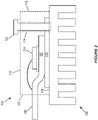
Figure 2 depicts an assembly that comprises a semiconductor package mounted on a heat sink, according to an embodiment. -
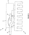
Figure 3 depicts an assembly that comprises a semiconductor package mounted on a heat sink, according to an embodiment. -
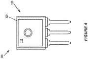
Figure 4 depicts a semiconductor device that comprises a semiconductor package and a releasable layer, according to an embodiment. -
Figure 5 depicts a semiconductor device that comprises a semiconductor package and a releasable layer, according to another embodiment. -
Figure 6 depicts a semiconductor device that comprises a semiconductor package and a releasable layer, according to another embodiment. -
Figure 7 depicts a lead frame strip that comprises multiple semiconductor packages and a continuous layer of releasable material attached to each package body on the lead frame strip. -
Figure 8 depicts a process flow that includes selected processing steps for producing a semiconductor device that comprises a semiconductor package and a releasable layer. - Disclosed herein is a semiconductor package with an advanced isolation structure and a releasable layer that advantageously protects the advanced isolation structure. The semiconductor package comprises an encapsulant material that in combination with the advanced isolation structure forms an electrically insulating package body that encapsulates a semiconductor die. The advanced isolation structure has a higher thermal conductivity than the encapsulant material. For example, the advanced isolation structure may comprise a thermal interface material (TIM) whereas the encapsulant material comprises mold compound. The advanced isolation structure is thermally coupled to the semiconductor die, thus providing a thermally efficient mechanism for extracting heat away from the semiconductor die. The material properties of the advanced isolation structure, while advantageous for thermal coupling, make it susceptible to damage such as scratching. The releasable layer is an advantageous temporary structure that protects the advanced isolation structure from damage. Moreover, the releasable layer can be easily removed by simple mechanical force before the semiconductor package is mounted.
- Referring to
Figure 1 , asemiconductor package 100 is depicted, according to an embodiment. Thesemiconductor package 100 comprises apackage body 102. Thepackage body 102 is an electrically insulating structure that encapsulates and electrically isolates a semiconductor die 104 (shown inFig. 2 ). Thesemiconductor package 100 comprises a plurality ofleads 106 that protrude out from thepackage body 102. The package leads 106 are electrically conductive structures that are configured to be inserted into a circuit carrier, such as a PCB. As shown, thesemiconductor package 100 comprises three of the package leads 106. More generally, thesemiconductor package 100 may comprise different numbers of the package leads 106, e.g., two, three, four, etc. - The
package body 102 comprises a firstouter face 108, a secondouter face 110, and outer edge sides 112 extending between the first and second outer faces 108, 110. The first and second outer faces 108, 110 may be the largest (area wise) surfaces of thepackage body 102. According to an embodiment, thesemiconductor package 100 comprises anopening 114 that extends between the first and second outer faces 108, 110. Theopening 114 may be dimensioned to receive afastener 114, e.g., in the manner depicted inFigure 2 . - According to an embodiment, the
semiconductor package 100 is configured as a discrete power device. A discrete power device refers to a single packaged device that is configured to block high voltages and and/or to conduct high currents as between two load terminals. Generally speaking, a discrete power device may be rated to block voltages of at least 100V, and more commonly on the order of 250V, 500V, 600V, 1,200V, 2,000V and/or may be rated to conduct currents of 10A, 50A, 100A, 500A or more. A discrete power device may comprise one or more semiconductor dies 104 connected between the two load terminals of thesemiconductor package 100. These semiconductor dies 104 may be configured as a discrete diode die, a discrete MOSFET (Metal Oxide Semiconductor Field Effect Transistor) die, a discrete IGBT (Insulated Gate Bipolar Transistor) die, a discrete HEMT (High Electron Mobility Transistors) die, a discrete JFET (Junction Field Effect Transistors) die, etc. These semiconductor dies 104 may be rated to block voltages of at least 100V, and more commonly on the order of 250V, 500V, 600V, 1,200V, 2,000V and/or may be rated to conduct currents of 10A, 50A, 100A, 500A or more. - In a particular embodiment of a discrete power device, the
semiconductor package 100 may be configured as a discrete transistor package. For example, thesemiconductor package 100 may be configured as a discrete IGBT, a discrete MOSFET, a discrete HEMT, etc. In these package types, the package leads 106 may correspond to the gate, source and drain terminals in the case of a MOSFET, the gate, emitter and collector terminals in the case of an IGBT, etc. A discrete transistor package may comprise a single transistor die or multiple transistor dies connected in parallel with one another so as to provide the equivalent functionality of a single transistor. Additionally or alternatively, a discrete transistor package may comprise a fourth lead that is configured as a sense terminal, (e.g., source-sense, drain-sense, etc.). - The
package body 102 comprises anencapsulant portion 116. Theencapsulant portion 116 is formed from a rigid and electrically insulating material that provides high voltage isolation. Examples of these materials include mold compound, thermosetting plastic, epoxy, resins, and laminate materials. Theencapsulant portion 116 can be formed by a molding process such as injection molding, compression molding, transfer molding, etc. Alternatively, theencapsulant portion 116 can be a laminate structure that is formed by successively stacking layers of laminate material on top of one another. - The
package body 102 additionally comprises anisolation structure 118. Theisolation structure 118 is an electrically insulating structure with higher thermal conductivity than theencapsulant portion 116. For example, theisolation structure 118 may have a thermal conductivity on the order of at least 1 W/mK (Watt per Meter-Kelvin), at least 2 W/mK, at least 3 W/mK, or at least 5 W/m, whereas theencapsulant portion 116 may have a thermal conductivity of no greater than 1 W/mK, or no greater than 0.1 W/mK. Theisolation structure 118 may comprise a thermal interface material (TIM), a thermal grease, or a phase change material. Examples of various configurations for the isolation structured 118 and/or materials for theisolation structure 118 are described in inUS Application 14/501,070 filed on September 30, 2014 US Application 15/333,993 filed on October 25, 2016 US Application 16/816,561 filed on March 12, 2020 isolation structure 118 comprises a silicone matrix and thermally conductive and electrically insulating filler particles suspended in the material. These filler particles may be a metal oxide and/or metal nitride, in particular at least one of SiO2 Al2O3, AIN, ZrO2, Si3N4, BN, diamond, etc. - The first
outer face 108 of thepackage body 102 comprises a first surface of theisolation structure 118. That is, theisolation structure 118 forms at least part of the firstouter face 108 of thepackage body 102. The first surface of theisolation structure 118 may be coplanar with a surface of theencapsulant portion 116 at the firstouter face 108. For example, theisolation structure 118 can be disposed within a recess formed within theencapsulant portion 116 such that theencapsulant portion 116 forms a ring that surrounds theisolation structure 118. More generally, the shape and arrangement of theisolation structure 118 may vary. For example, theisolation structure 118 may form a complete outer face of thepackage body 102 and/or may be exposed at multiple faces of thepackage body 102. - Referring to
Fig. 2 , an assembly that comprises thesemiconductor package 100 and aheat sink 200 is shown. Thesemiconductor package 100 is mounted on theheat sink 200 with the firstouter face 108 of thepackage body 102 flush against theheat sink 200. Thesemiconductor package 100 comprises adie pad 120 and asemiconductor die 104 that is mounted on thedie pad 120. Thedie pad 120 and theleads 106 may be collectively provided from a lead frame formed of metal, such as copper (Cu), aluminum (Al), nickel (Ni), silver (Ag), palladium (Pd), gold (Au), etc., alloys or combinations thereof. A terminal of the semiconductor die 104 (e.g., a drain, collector, etc.) is electrically connected to one of theleads 106 via thedie pad 120 and additional terminals of the semiconductor die 104 (e.g. source, emitter, gate, etc.) are electrically connected to theleads 106 by bond wires. More generally, any of a variety of interconnect elements such as ribbons, clips, etc. may be used to complete the electrical connections between the semiconductor die 104 and theleads 106. - The
semiconductor package 100 is mounted to theheat sink 200 such that thedie pad 120 and theisolation structure 118 provide a thermally conductive path that transfers heat between the semiconductor die 104 and theheat sink 200. Theisolation structure 118 is thermally coupled to the semiconductor die 104 via thedie pad 120, which in turn is thermally coupled to the semiconductor die 104. This thermal conduction path may also comprise adhesives and intermediary materials, e.g., solder, conductive glue, etc. The high thermal conductivity of theisolation structure 118 allows for efficient heat transfer between the semiconductor die 104 and theheat sink 200. Moreover, the electrically insulating properties of theisolation structure 118 mean that the semiconductor die 104 is electrically isolated from theheat sink 200, which allows for high voltage operation of the semiconductor die 104. Thesemiconductor package 100 may be mounted by afastener 122, e.g., screw, pin, bolt, etc. Thefastener 122 may extend completely through theopening 114 and be received by theheat sink 200. Additionally or alternatively, the fastener and theopening 114 may be may be used in combination with an external clip to secure thesemiconductor package 100 to theheat sink 200. - The
isolation structure 118 may be a relatively soft structure. For example, theisolation structure 118 may have a compressibility in a range between 1% and 40% (which may be measured by applying a 1 N force at a layer of the interface structure having a thickness of 250 µm using a Vickers-micro-indenter), in particular in a range between 25% and 35%. When theisolation structure 118 is brought in contact with theheat sink 200, the soft material properties of theisolation structure 118 ensure a proper full-surface contact and thus an efficient heat transfer from theisolation structure 118 toheat sink 200. In particular, it may be sufficient to directly connect theisolation structure 118 with theheat sink 200 using thefastener 122, and in particular without the need of thermal grease in between the thermal interface structure and theheat sink 200. By contrast, theencapsulant portion 116 has a greater hardness than theisolation structure 118. For example, anencapsulant portion 116 formed from any of the above-listed materials (e.g., mold compound, thermosetting plastic, epoxy, resins, laminate materials, etc.) may have a compressibility of less than 5%, and more commonly less than 1%, less than 0.5%, or less than 0.1% on the same measurement under the using a Vickers-micro-indenter. This difference in hardness is attributable to the different material composition of theisolation structure 118 and theencapsulant portion 116. - The mechanical properties of the
isolation structure 118 are such that thesemiconductor package 100 is susceptible to damage, particularly in the time between the manufacture of thesemiconductor package 100 and when thesemiconductor package 100 is mounted in an assembly (e.g., as shown inFig. 2 ). At this time, thesemiconductor package 100 may be tested and handled by testing equipment, packaged for shipping, transported from a manufacturer to a customer, removed from the shipping packaging, and mounted on a customer apparatus such as a heat sink and/or circuit board. A mechanical stimulus applied by humans and/or machines during any of these steps may form scratches, cracks and other imperfections may arise in theisolation structure 118. This damage may degrade performance and/or render thesemiconductor package 100 dysfunctional. - Referring to
Fig. 3 , an assembly that comprises thesemiconductor package 100 and aheat sink 200 is shown, according to another embodiment. Thesemiconductor package 100 is substantially similar to the embodiment shown inFigures 1-2 , with the following exceptions. One difference is that there is noopening 114 provided in thepackage body 102. In this case, thepackage body 102 may be configured such that theencapsulant portion 116 is a continuous region of mold compound that covers and protects the semiconductor die 104. Thissemiconductor package 100 may be secured to theheat sink 200 using a clip structure. A second difference in this assembly is that the firstouter face 108 of theencapsulant portion 116 is a completely planar surface, and theisolation structure 118 is disposed on this planar surface. That is, there is no recess in the encapsulant material that accommodates theisolation structure 118. Various embodiments of thesemiconductor package 100 and the assembly may incorporate either one of the above-mentioned differences. - Referring to
Figure 4 , asemiconductor device 300 that comprises areleasable layer 400 affixed to thesemiconductor package 100 is depicted, according to an embodiment. When thereleasable layer 400 is affixed to thesemiconductor package 100 and covering theisolation structure 118, it provides a protective sheath that prevents scratching or defacing of theisolation structure 118. Thus, thereleasable layer 400 substantially mitigates or eliminates the above-described damage that may occur in the time between the manufacture of thesemiconductor package 100 and when thesemiconductor package 100 is mounted in an assembly. As shown, thereleasable layer 400 completely covers the first surface of theisolation structure 118, and thus completely protects all exposed surfaces of theisolation structure 118. In the case that thesemiconductor package 100 comprises theopening 114, thereleasable layer 400 may extend over theopening 114 as well. In the case that theisolation structure 118 is disposed within a recess formed within theencapsulant portion 116, thereleasable layer 400 may extend past theisolation structure 118 such that thereleasable layer 400 may partially cover and be releasable from the firstouter face 108 of theencapsulant portion 116. In the case that theisolation structure 118 is disposed outside of the plane of firstouter face 108 of theencapsulant portion 116, thereleasable layer 400 may exclusively contact theisolation structure 118. More generally, thereleasable layer 400 may at least partially cover any exposed surface of an isolation material, thus providing the protective benefit as described herein, and may also contact and be releasable from other adjacent surfaces of thesemiconductor package 100 - The
releasable layer 400 is releasable from thesemiconductor package 100. This means that thereleasable layer 400 is a temporary element that can be removed from thesemiconductor package 100 by mechanical force, e.g., human hand manipulation or robotic motion, that is non-destructive to all elements of thesemiconductor package 100 including theisolation structure 118. Thereleasable layer 400 may be a relatively thin film (e.g., between 0.1 - 0.01 mm thick) that is adhesively bonded to thesemiconductor package 100. The strength of the adhesive that secures thereleasable layer 400 to thesemiconductor package 100 is selected such that thereleasable layer 400 can be removed, e.g., by peeling, without substantially damaging or altering theisolation structure 118. In this way, thereleasable layer 400 can be applied to thesemiconductor package 100 once manufacture is complete and easily removed by a downstream user, e.g., by removing thereleasable layer 400 immediately before mounting thesemiconductor package 100. - According to one embodiment, the
releasable layer 400 comprises an adhesive tape. For example, thereleasable layer 400 can comprise a non-conductive adhesive tape, e.g., a tape comprising polymer, rubber, silicone, etc. with a thickness between 0.1 - 0.01 mm. This adhesive tape can be adhered to thesemiconductor package 100 in a commonly known manner by applying the adhesive side of the adhesive tape to the firstouter face 108 of thepackage body 102. - According to another embodiment, the releasable is layer a non-adhesive film. For example, the
releasable layer 400 can be film of non-conductive material comprising polymer, rubber, silicone with a thickness between 0.1 mm and .01 mm. This film can be secured to the package by separately applying an electrically insulating adhesive such as an epoxy-based or silicone-based adhesive to the firstouter face 108 of thepackage body 102 and subsequently attaching the film to the electrically insulating adhesive. - Referring to
Figure 5 , asemiconductor device 300 that comprises areleasable layer 400 affixed to thesemiconductor package 100 is depicted, according to another embodiment. In this embodiment, thereleasable layer 400 comprises amain portion 402 and atab 404. Themain portion 402 is adhered to and releasable from a portion of the firstouter face 108 of thepackage body 102 that comprises the first surface of theisolation structure 118. Thus, themain portion 402 protects theisolation structure 118 in a similar manner as previously described. Thetab 404 is connected to themain portion 402 and is decoupled from thepackage body 102. That is, thetab 404 is not adhered to any surface of thepackage body 102. As a result, thetab 404 provides a handle that can be grasped, e.g., by a human hand or robotic hand. Thetab 404 therefore allows for easy releasing (e.g., peeling) of thereleasable layer 400 by providing a surface from which to grip thereleasable layer 400. As shown, thetab 404 extends away from thepackage body 102 in an opposite direction as the leads 106. - Referring to
Figure 6 , asemiconductor device 300 that comprises areleasable layer 400 affixed to thesemiconductor package 100 is depicted, according to another embodiment. The embodiment offigure 5 is substantially identical to that ofFigure 4 , except that the orientation of thereleasable layer 400 is reversed such that thetab 404 extends away from thepackage body 102 in the same direction as the leads 106. This represents one other potential arrangement for areleasable layer 400 that comprises atab 404. More generally, the orientation, number, and geometry of the tab 404 (or tabs) may vary from the specific embodiments shown inFigures 4 and5 . For example, thetab 404 may have any desired shape, and may be designed to be compatible with a particular apparatus for removing thereleasable layer 400. Additionally or alternatively, thereleasable layer 400 may havemultiple tabs 404, e.g., for purposes of redundancy. - Referring to
Figure 7 , an assembly for forming thesemiconductor package 100 is shown. The assembly comprises alead frame strip 124 that comprises a plurality of unit lead frames 126. Each of the unit lead frames 126 comprises a die pad 120 (e.g., as shown inFig. 2 ) and a plurality ofleads 106, thereby providing the lead frame configuration of thesemiconductor package 100 as previously described with reference toFig. 1 . The assembly shown inFigure 6 corresponds to an intermediate phase of manufacture before theleads 106 are detached from aperipheral structure 128 of thelead frame strip 124. - In the assembly of
Figure 7 , acontinuous layer 408 of releasable material is applied to the firstouter face 108 of eachpackage body 102. That is, one strip of material is used to provide thereleasable layer 400 for eachsemiconductor package 100. Thecontinuous layer 408 can be a layer of an adhesive tape, e.g., as previously described. Alternatively, thecontinuous layer 408 can be a non-adhesive film that is bonded to thesemiconductor package 100 by a separate adhesive, e.g., as previously described. - Referring to
Figure 8 , a process flow for a method of producing asemiconductor device 300 comprising thesemiconductor package 100 is depicted, according to an embodiment. - In a
first process step 500, the semiconductor dies 104 are attached to thedie pads 120 for each of the unit lead frames 126. This may be done by soldering, for example. - In a
second process step 502, a wire bonding process is performed to form the bond wires for each of the unit lead frames 126. - In a
third process step 504, a molding process is performed. The molding process forms theencapsulant portion 116 of thepackage body 102, e.g., by a transfer molding technique. - In a
fourth processing step 506, a post mold cure is performed so as to harden theencapsulant portion 116 of thepackage body 102. - In a
fifth process step 508, a second molding process is performed. The second molding process forms the isolation portion of thepackage body 102, e.g., by a compression molding technique. - In a
sixth processing step 510, a post mold cure if performed so as to harden the isolation portion of thepackage body 102. - In a
seventh process step 512, a deflashing step is performed. The deflashing step removes mold flashes, i.e., excess portions or strands of mold material, from thepackage body 102. The deflashing may be done using a chemical solvent, for example. - In an
eighth process step 514, an adhesive layer masking step is performed. The adhesive layer masking step applies acontinuous layer 408 of releasable material to the firstouter face 108 of eachpackage body 102, e.g., in the manner depicted inFigure 6 . - In a
ninth process step 516, the adhesive layer is cured to thesemiconductor package 100. This curing may involve the application of ultraviolet light, for example. - In a
tenth process step 518, a plating process is performed. The plating process forms a metal plating (e.g., Ag, Cu, Ni, etc.) on the exposed metal leads 106 of eachsemiconductor package 100. The plating process may comprise an electroplating process or an electroless plating technique, for example. - In an
eleventh process step 520, an adhesive layer cutting step is performed. The adhesive layer cuts thecontinuous layer 408 of releasable material to form thereleasable layer 400 for each of the semiconductor packages 100. This may be done by cutting thecontinuous layer 408 along aseparation line 130, e.g., as shown inFig. 6 . - In a
twelfth process step 522, a package singulation step is performed. The package singulation step separates eachsemiconductor package 100 from thelead frame strip 124, e.g., by cutting theleads 106 so as to detach them from theperipheral structure 128. Advantageously, thereleasable layer 400 is present on theisolation structure 118 during this step such that the package singulation step does not scratch the isolation structure. - In a
thirteenth process step 524, thesemiconductor package 100 is tested. For example, the electrical functionality of thesemiconductor package 100 and/or the electrical isolation of theisolation structure 118 may be tested by test equipment. Advantageously, thereleasable layer 400 is present on theisolation structure 118 during this step such that the testing step does not scratch the isolation structure. - In a
fourteenth process step 526, thesemiconductor package 100 is arranged in packaging for transport, e.g., by arranging thesemiconductor package 100 in plastic, cardboard, Styrofoam, etc. Advantageously, thereleasable layer 400 is present on theisolation structure 118 during this step such that the packaging step does not scratch the isolation structure. - The
semiconductor package 100 disclosed herein illustrates just one example of a semiconductor package that includes an advanced isolation material thermally coupled to a semiconductor die. Thereleasable layer 400 described herein is more generally applicable to any type of semiconductor package that comprises a region of isolation material that is softer and more susceptible to scratching or other types of damage than conventional encapsulant material. - Spatially relative terms such as "under," "below," "lower," "over," "upper" and the like, are used for ease of description to explain the positioning of one element relative to a second element. These terms are intended to encompass different orientations of the device in addition to different orientations than those depicted in the figures. Further, terms such as "first," "second," and the like, are also used to describe various elements, regions, sections, etc. and are also not intended to be limiting. Like terms refer to like elements throughout the description.
- As used herein, the terms "having," "containing," "including," "comprising" and the like are open-ended terms that indicate the presence of stated elements or features, but do not preclude additional elements or features. The articles "a," "an" and "the" are intended to include the plural as well as the singular, unless the context clearly indicates otherwise.
- With the above range of variations and applications in mind, it should be understood that the present invention is not limited by the foregoing description, nor is it limited by the accompanying drawings. Instead, the present invention is limited only by the following claims and their legal equivalents.
Claims (15)
- A semiconductor device, comprising:a semiconductor package, comprising a package body that comprises an encapsulant portion and an isolation structure, a semiconductor die embedded within the package body, and a plurality of leads that protrude out from the encapsulant body, wherein the encapsulant portion and the isolation structure are each electrically insulating structures, wherein the isolation structure has a greater thermal conductivity than the encapsulant portion, and wherein the isolation structure is thermally coupled to the semiconductor die; anda releasable layer affixed to the semiconductor package;wherein a first outer face of the package body comprises a first surface of the isolation structure,wherein the releasable layer at least partially covers the first surface of the isolation structure, andwherein the releasable layer is releasable from the semiconductor package.
- The semiconductor device of claim 1, wherein the encapsulant portion has a greater hardness than the isolation structure.
- The semiconductor device of claim 2, wherein the encapsulant portion comprises a mold compound, and wherein the isolation structure comprises thermal interface material.
- The semiconductor device of one of the preceding claims, wherein the releasable layer completely covers and is releasable from the first surface of the isolation structure.
- The semiconductor device of claim 3, wherein the first outer face of the package body further comprises a first surface of the encapsulant portion that surrounds the isolation structure, and wherein the releasable layer at least partially covers and is releasable from the first surface of the encapsulant portion.
- The semiconductor device of claim 3, further comprising an opening in the package body that extends through the isolation structure and the encapsulant portion, and wherein the releasable layer extends over the opening.
- The semiconductor device of one of the preceding claims, wherein the releasable layer is an adhesive tape that is adhered to and releasable from the first surface of the isolation structure.
- The semiconductor device of one of the preceding claims, wherein the releasable layer comprises a main portion and a tab, wherein the main portion is adhered to and releasable from the first surface of the isolation structure, and wherein the tab is connected to the main portion and is decoupled from the package body.
- The semiconductor device of claim 7, wherein the tab extends away from the package body in an opposite direction as the leads, or wherein the tab extends away from the package body in the same direction as the leads.
- The semiconductor device of one of the preceding claims, wherein the semiconductor package further comprises a die pad, wherein the semiconductor die is mounted on the die pad, and wherein the isolation structure is thermally coupled to the semiconductor die via the die pad.
- A method of producing a semiconductor device, the method comprising:providing a semiconductor package, the semiconductor package comprising a package body that comprises an encapsulant portion and an isolation structure, a semiconductor die embedded within the package body, and a plurality of leads that protrude out from the encapsulant body, wherein the isolation structure has a greater thermal conductivity than the encapsulant portion, wherein the isolation structure is thermally coupled to the semiconductor die, and wherein a first outer face of the package body comprises a first surface of the isolation structure,applying a releasable layer to the first outer face of the package body such that the releasable layer at least partially covers the first surface of the isolation structure,wherein the releasable layer is configured to substantially protect the isolation structure from damage during transport and assembly, andwherein the releasable layer is releasable from the package body by mechanical force.
- The method of claim 11, wherein providing the semiconductor package comprises:providing a lead frame strip that comprises a plurality of unit lead frames, each of the unit lead frames comprising a die pad and a plurality of leads that are each connected to a peripheral structure of the lead frame strip;attaching one of the semiconductor dies on each of the unit lead frames; andforming the package body on each of the each of the unit lead frames, andwherein applying the releasable layer comprises:
attaching a continuous layer of releasable material to each package body on the lead frame strip. - The method of claim 12, further comprising:cutting the continuous layer to form separated ones of the releasable layers for each package body on the lead frame strip, andseparating the unit lead frames from the peripheral structure of the lead frame strip after cutting the continuous layer.
- The method of claim 12 or 13, wherein forming the package body comprises a molding process, wherein the method further comprises:performing a deflashing step after the molding process that removes excess mold material from the package body, andperforming a plating process that forms a metal plating on the leads, andwherein the applying of the releasable layer comprises attaching the continuous layer in between the deflashing step and the plating process.
- The method of one of claims 12 to 14, wherein the releasable layer comprises a non-adhesive film, and wherein applying the releasable layer comprises applying an adhesive to the first surface of the isolation structure after forming the package body and attaching the non-adhesive film to the adhesive.
Applications Claiming Priority (1)
| Application Number | Priority Date | Filing Date | Title |
|---|---|---|---|
| US17/355,342 US11791238B2 (en) | 2021-06-23 | 2021-06-23 | Semiconductor package with releasable isolation layer protection |
Publications (2)
| Publication Number | Publication Date |
|---|---|
| EP4109519A2 true EP4109519A2 (en) | 2022-12-28 |
| EP4109519A3 EP4109519A3 (en) | 2023-01-11 |
Family
ID=82494034
Family Applications (1)
| Application Number | Title | Priority Date | Filing Date |
|---|---|---|---|
| EP22179091.8A Pending EP4109519A3 (en) | 2021-06-23 | 2022-06-15 | Semiconductor package with releasable isolation layer protection |
Country Status (3)
| Country | Link |
|---|---|
| US (2) | US11791238B2 (en) |
| EP (1) | EP4109519A3 (en) |
| CN (1) | CN115513151A (en) |
Family Cites Families (26)
| Publication number | Priority date | Publication date | Assignee | Title |
|---|---|---|---|---|
| US6143076A (en) | 1996-06-21 | 2000-11-07 | Thermalloy Inc. | Applicator head |
| KR100370231B1 (en) * | 2000-06-13 | 2003-01-29 | 페어차일드코리아반도체 주식회사 | Power module package having a insulator type heat sink attached a backside of leadframe & manufacturing method thereof |
| JP2002084083A (en) | 2000-07-06 | 2002-03-22 | Fuji Kobunshi Kogyo Kk | Heat dissipation sheet products |
| JP2005353805A (en) | 2004-06-10 | 2005-12-22 | Toshiba Corp | Semiconductor device and manufacturing method thereof |
| CN2778815Y (en) | 2005-01-17 | 2006-05-10 | 天津加藤精密电子有限公司 | Connecting adhesive tape with stripping ears for conveying and taping surface mounted devices |
| US20080036078A1 (en) * | 2006-08-14 | 2008-02-14 | Ciclon Semiconductor Device Corp. | Wirebond-less semiconductor package |
| KR101524545B1 (en) * | 2008-02-28 | 2015-06-01 | 페어차일드코리아반도체 주식회사 | Power device package and the method of fabricating the same |
| US8049312B2 (en) * | 2009-01-12 | 2011-11-01 | Texas Instruments Incorporated | Semiconductor device package and method of assembly thereof |
| US8940122B2 (en) | 2010-03-12 | 2015-01-27 | Wrapsol Acquisition, Llc | Protective adhesive film, method of adhering protective adhesive film to a device, and device comprising protective adhesive film |
| US8349658B2 (en) * | 2010-05-26 | 2013-01-08 | Stats Chippac, Ltd. | Semiconductor device and method of forming conductive posts and heat sink over semiconductor die using leadframe |
| CN103155109B (en) | 2010-10-15 | 2017-08-11 | 日立化成株式会社 | Tape for wafer processing, method of manufacturing tape for wafer processing, and method of manufacturing semiconductor device |
| US8044942B1 (en) | 2011-01-18 | 2011-10-25 | Aevoe Inc. | Touch screen protector |
| JP5936310B2 (en) * | 2011-03-17 | 2016-06-22 | 三菱電機株式会社 | Power semiconductor module and its mounting structure |
| JP6114184B2 (en) * | 2011-04-04 | 2017-04-12 | ローム株式会社 | Semiconductor device and manufacturing method of semiconductor device |
| JP2013070026A (en) * | 2011-09-08 | 2013-04-18 | Rohm Co Ltd | Semiconductor device, manufacturing method of semiconductor device, mounting structure of semiconductor device, and power semiconductor device |
| JP6076675B2 (en) * | 2011-10-31 | 2017-02-08 | ローム株式会社 | Semiconductor device |
| DE102013220880B4 (en) | 2013-10-15 | 2016-08-18 | Infineon Technologies Ag | An electronic semiconductor package having an electrically insulating, thermal interface structure on a discontinuity of an encapsulation structure, and a manufacturing method therefor, and an electronic device having the same |
| CN104789150A (en) | 2015-04-27 | 2015-07-22 | 苏州佳值电子工业有限公司 | Fully-automatic adhesion double sided adhesive tape for flexible board project and corresponding coiling product |
| DE102015116807A1 (en) | 2015-10-02 | 2017-04-06 | Infineon Technologies Austria Ag | Functionalized interface structure |
| DE102015118245B4 (en) | 2015-10-26 | 2024-10-10 | Infineon Technologies Austria Ag | Electronic component with a thermal interface material, manufacturing method for an electronic component, heat dissipation body with a thermal interface material and thermal interface material |
| US10727151B2 (en) * | 2017-05-25 | 2020-07-28 | Infineon Technologies Ag | Semiconductor chip package having a cooling surface and method of manufacturing a semiconductor package |
| EP3709346B1 (en) | 2019-03-15 | 2023-01-18 | Infineon Technologies Austria AG | An electronic module comprising a semiconductor package with integrated clip and fastening element |
| US10879155B2 (en) * | 2019-05-09 | 2020-12-29 | Texas Instruments Incorporated | Electronic device with double-sided cooling |
| US11302615B2 (en) * | 2019-12-30 | 2022-04-12 | Texas Instruments Incorporated | Semiconductor package with isolated heat spreader |
| EP3872851B1 (en) | 2020-02-27 | 2025-04-30 | Infineon Technologies Austria AG | Protection cap for package with thermal interface material |
| US11910518B2 (en) * | 2021-05-26 | 2024-02-20 | Huawei Technologies Canada Co., Ltd. | Method and apparatus for heat sink mounting |
-
2021
- 2021-06-23 US US17/355,342 patent/US11791238B2/en active Active
-
2022
- 2022-06-15 EP EP22179091.8A patent/EP4109519A3/en active Pending
- 2022-06-23 CN CN202210717818.XA patent/CN115513151A/en active Pending
-
2023
- 2023-08-18 US US18/235,668 patent/US12080625B2/en active Active
Also Published As
| Publication number | Publication date |
|---|---|
| US20230395462A1 (en) | 2023-12-07 |
| EP4109519A3 (en) | 2023-01-11 |
| US11791238B2 (en) | 2023-10-17 |
| US12080625B2 (en) | 2024-09-03 |
| US20220415753A1 (en) | 2022-12-29 |
| CN115513151A (en) | 2022-12-23 |
Similar Documents
| Publication | Publication Date | Title |
|---|---|---|
| US10283432B2 (en) | Molded package with chip carrier comprising brazed electrically conductive layers | |
| US9054063B2 (en) | High power single-die semiconductor package | |
| US8709875B2 (en) | Power device and method of packaging same | |
| US9478484B2 (en) | Semiconductor packages and methods of formation thereof | |
| US20160358838A1 (en) | Semiconductor Power Package and Method of Manufacturing the Same | |
| US20100052149A1 (en) | Semiconductor device and method of manufacturing the same | |
| US20020025607A1 (en) | Semiconductor device and a method of manufacturing the same | |
| US9082759B2 (en) | Semiconductor packages and methods of formation thereof | |
| US11626351B2 (en) | Semiconductor package with barrier to contain thermal interface material | |
| CN103928411B (en) | Chip apparatus and its manufacture method, integrated circuit and its manufacture method | |
| CN103426837B (en) | Semiconductor packages and the method for forming semiconductor packages | |
| EP3709346B1 (en) | An electronic module comprising a semiconductor package with integrated clip and fastening element | |
| US20200411421A1 (en) | Semiconductor device assemblies | |
| US20140353812A1 (en) | Semiconductor device | |
| CN103681531A (en) | Integrated circuits and method for manufacturing integrated circuit | |
| US12080625B2 (en) | Semiconductor package with releasable isolation layer protection | |
| US7579680B2 (en) | Packaging system for semiconductor devices | |
| JP2001118961A (en) | Resin-sealed power semiconductor device and method of manufacturing the same | |
| CN101819955B (en) | Semiconductor packaging structure with reinforced heat dissipation property | |
| US20140264944A1 (en) | Semiconductor Package with Top-Side Insulation Layer | |
| US8859333B2 (en) | Integrated circuit package and a method for dissipating heat in an integrated circuit package | |
| US20250218914A1 (en) | Package with component-carrying intermediate structure and additional carrier having reference potential structure | |
| JPH077112A (en) | Resin-sealed semiconductor device | |
| CN117790417A (en) | Semiconductor circuit and device manufacturing method, wafer composite and semiconductor device |
Legal Events
| Date | Code | Title | Description |
|---|---|---|---|
| PUAI | Public reference made under article 153(3) epc to a published international application that has entered the european phase |
Free format text: ORIGINAL CODE: 0009012 |
|
| STAA | Information on the status of an ep patent application or granted ep patent |
Free format text: STATUS: THE APPLICATION HAS BEEN PUBLISHED |
|
| PUAL | Search report despatched |
Free format text: ORIGINAL CODE: 0009013 |
|
| AK | Designated contracting states |
Kind code of ref document: A2 Designated state(s): AL AT BE BG CH CY CZ DE DK EE ES FI FR GB GR HR HU IE IS IT LI LT LU LV MC MK MT NL NO PL PT RO RS SE SI SK SM TR |
|
| AK | Designated contracting states |
Kind code of ref document: A3 Designated state(s): AL AT BE BG CH CY CZ DE DK EE ES FI FR GB GR HR HU IE IS IT LI LT LU LV MC MK MT NL NO PL PT RO RS SE SI SK SM TR |
|
| RIC1 | Information provided on ipc code assigned before grant |
Ipc: H01L 23/495 20060101ALI20221202BHEP Ipc: H01L 23/433 20060101AFI20221202BHEP |
|
| STAA | Information on the status of an ep patent application or granted ep patent |
Free format text: STATUS: REQUEST FOR EXAMINATION WAS MADE |
|
| 17P | Request for examination filed |
Effective date: 20230710 |
|
| RBV | Designated contracting states (corrected) |
Designated state(s): AL AT BE BG CH CY CZ DE DK EE ES FI FR GB GR HR HU IE IS IT LI LT LU LV MC MK MT NL NO PL PT RO RS SE SI SK SM TR |