EP4109442A1 - Gate driver, organic light emitting display device and driving method thereof - Google Patents
Gate driver, organic light emitting display device and driving method thereof Download PDFInfo
- Publication number
- EP4109442A1 EP4109442A1 EP22173013.8A EP22173013A EP4109442A1 EP 4109442 A1 EP4109442 A1 EP 4109442A1 EP 22173013 A EP22173013 A EP 22173013A EP 4109442 A1 EP4109442 A1 EP 4109442A1
- Authority
- EP
- European Patent Office
- Prior art keywords
- gate
- mode
- low voltage
- voltage
- signal
- Prior art date
- Legal status (The legal status is an assumption and is not a legal conclusion. Google has not performed a legal analysis and makes no representation as to the accuracy of the status listed.)
- Pending
Links
Images




Classifications
-
- G—PHYSICS
- G09—EDUCATION; CRYPTOGRAPHY; DISPLAY; ADVERTISING; SEALS
- G09G—ARRANGEMENTS OR CIRCUITS FOR CONTROL OF INDICATING DEVICES USING STATIC MEANS TO PRESENT VARIABLE INFORMATION
- G09G3/00—Control arrangements or circuits, of interest only in connection with visual indicators other than cathode-ray tubes
- G09G3/20—Control arrangements or circuits, of interest only in connection with visual indicators other than cathode-ray tubes for presentation of an assembly of a number of characters, e.g. a page, by composing the assembly by combination of individual elements arranged in a matrix no fixed position being assigned to or needed to be assigned to the individual characters or partial characters
- G09G3/22—Control arrangements or circuits, of interest only in connection with visual indicators other than cathode-ray tubes for presentation of an assembly of a number of characters, e.g. a page, by composing the assembly by combination of individual elements arranged in a matrix no fixed position being assigned to or needed to be assigned to the individual characters or partial characters using controlled light sources
- G09G3/30—Control arrangements or circuits, of interest only in connection with visual indicators other than cathode-ray tubes for presentation of an assembly of a number of characters, e.g. a page, by composing the assembly by combination of individual elements arranged in a matrix no fixed position being assigned to or needed to be assigned to the individual characters or partial characters using controlled light sources using electroluminescent panels
- G09G3/32—Control arrangements or circuits, of interest only in connection with visual indicators other than cathode-ray tubes for presentation of an assembly of a number of characters, e.g. a page, by composing the assembly by combination of individual elements arranged in a matrix no fixed position being assigned to or needed to be assigned to the individual characters or partial characters using controlled light sources using electroluminescent panels semiconductive, e.g. using light-emitting diodes [LED]
- G09G3/3208—Control arrangements or circuits, of interest only in connection with visual indicators other than cathode-ray tubes for presentation of an assembly of a number of characters, e.g. a page, by composing the assembly by combination of individual elements arranged in a matrix no fixed position being assigned to or needed to be assigned to the individual characters or partial characters using controlled light sources using electroluminescent panels semiconductive, e.g. using light-emitting diodes [LED] organic, e.g. using organic light-emitting diodes [OLED]
- G09G3/3266—Details of drivers for scan electrodes
-
- G—PHYSICS
- G09—EDUCATION; CRYPTOGRAPHY; DISPLAY; ADVERTISING; SEALS
- G09G—ARRANGEMENTS OR CIRCUITS FOR CONTROL OF INDICATING DEVICES USING STATIC MEANS TO PRESENT VARIABLE INFORMATION
- G09G3/00—Control arrangements or circuits, of interest only in connection with visual indicators other than cathode-ray tubes
- G09G3/20—Control arrangements or circuits, of interest only in connection with visual indicators other than cathode-ray tubes for presentation of an assembly of a number of characters, e.g. a page, by composing the assembly by combination of individual elements arranged in a matrix no fixed position being assigned to or needed to be assigned to the individual characters or partial characters
- G09G3/22—Control arrangements or circuits, of interest only in connection with visual indicators other than cathode-ray tubes for presentation of an assembly of a number of characters, e.g. a page, by composing the assembly by combination of individual elements arranged in a matrix no fixed position being assigned to or needed to be assigned to the individual characters or partial characters using controlled light sources
- G09G3/30—Control arrangements or circuits, of interest only in connection with visual indicators other than cathode-ray tubes for presentation of an assembly of a number of characters, e.g. a page, by composing the assembly by combination of individual elements arranged in a matrix no fixed position being assigned to or needed to be assigned to the individual characters or partial characters using controlled light sources using electroluminescent panels
- G09G3/32—Control arrangements or circuits, of interest only in connection with visual indicators other than cathode-ray tubes for presentation of an assembly of a number of characters, e.g. a page, by composing the assembly by combination of individual elements arranged in a matrix no fixed position being assigned to or needed to be assigned to the individual characters or partial characters using controlled light sources using electroluminescent panels semiconductive, e.g. using light-emitting diodes [LED]
- G09G3/3208—Control arrangements or circuits, of interest only in connection with visual indicators other than cathode-ray tubes for presentation of an assembly of a number of characters, e.g. a page, by composing the assembly by combination of individual elements arranged in a matrix no fixed position being assigned to or needed to be assigned to the individual characters or partial characters using controlled light sources using electroluminescent panels semiconductive, e.g. using light-emitting diodes [LED] organic, e.g. using organic light-emitting diodes [OLED]
-
- G—PHYSICS
- G06—COMPUTING OR CALCULATING; COUNTING
- G06F—ELECTRIC DIGITAL DATA PROCESSING
- G06F1/00—Details not covered by groups G06F3/00 - G06F13/00 and G06F21/00
- G06F1/04—Generating or distributing clock signals or signals derived directly therefrom
-
- G—PHYSICS
- G09—EDUCATION; CRYPTOGRAPHY; DISPLAY; ADVERTISING; SEALS
- G09G—ARRANGEMENTS OR CIRCUITS FOR CONTROL OF INDICATING DEVICES USING STATIC MEANS TO PRESENT VARIABLE INFORMATION
- G09G3/00—Control arrangements or circuits, of interest only in connection with visual indicators other than cathode-ray tubes
- G09G3/20—Control arrangements or circuits, of interest only in connection with visual indicators other than cathode-ray tubes for presentation of an assembly of a number of characters, e.g. a page, by composing the assembly by combination of individual elements arranged in a matrix no fixed position being assigned to or needed to be assigned to the individual characters or partial characters
- G09G3/22—Control arrangements or circuits, of interest only in connection with visual indicators other than cathode-ray tubes for presentation of an assembly of a number of characters, e.g. a page, by composing the assembly by combination of individual elements arranged in a matrix no fixed position being assigned to or needed to be assigned to the individual characters or partial characters using controlled light sources
- G09G3/30—Control arrangements or circuits, of interest only in connection with visual indicators other than cathode-ray tubes for presentation of an assembly of a number of characters, e.g. a page, by composing the assembly by combination of individual elements arranged in a matrix no fixed position being assigned to or needed to be assigned to the individual characters or partial characters using controlled light sources using electroluminescent panels
- G09G3/32—Control arrangements or circuits, of interest only in connection with visual indicators other than cathode-ray tubes for presentation of an assembly of a number of characters, e.g. a page, by composing the assembly by combination of individual elements arranged in a matrix no fixed position being assigned to or needed to be assigned to the individual characters or partial characters using controlled light sources using electroluminescent panels semiconductive, e.g. using light-emitting diodes [LED]
- G09G3/3208—Control arrangements or circuits, of interest only in connection with visual indicators other than cathode-ray tubes for presentation of an assembly of a number of characters, e.g. a page, by composing the assembly by combination of individual elements arranged in a matrix no fixed position being assigned to or needed to be assigned to the individual characters or partial characters using controlled light sources using electroluminescent panels semiconductive, e.g. using light-emitting diodes [LED] organic, e.g. using organic light-emitting diodes [OLED]
- G09G3/3225—Control arrangements or circuits, of interest only in connection with visual indicators other than cathode-ray tubes for presentation of an assembly of a number of characters, e.g. a page, by composing the assembly by combination of individual elements arranged in a matrix no fixed position being assigned to or needed to be assigned to the individual characters or partial characters using controlled light sources using electroluminescent panels semiconductive, e.g. using light-emitting diodes [LED] organic, e.g. using organic light-emitting diodes [OLED] using an active matrix
-
- G—PHYSICS
- G09—EDUCATION; CRYPTOGRAPHY; DISPLAY; ADVERTISING; SEALS
- G09G—ARRANGEMENTS OR CIRCUITS FOR CONTROL OF INDICATING DEVICES USING STATIC MEANS TO PRESENT VARIABLE INFORMATION
- G09G3/00—Control arrangements or circuits, of interest only in connection with visual indicators other than cathode-ray tubes
- G09G3/20—Control arrangements or circuits, of interest only in connection with visual indicators other than cathode-ray tubes for presentation of an assembly of a number of characters, e.g. a page, by composing the assembly by combination of individual elements arranged in a matrix no fixed position being assigned to or needed to be assigned to the individual characters or partial characters
- G09G3/22—Control arrangements or circuits, of interest only in connection with visual indicators other than cathode-ray tubes for presentation of an assembly of a number of characters, e.g. a page, by composing the assembly by combination of individual elements arranged in a matrix no fixed position being assigned to or needed to be assigned to the individual characters or partial characters using controlled light sources
- G09G3/30—Control arrangements or circuits, of interest only in connection with visual indicators other than cathode-ray tubes for presentation of an assembly of a number of characters, e.g. a page, by composing the assembly by combination of individual elements arranged in a matrix no fixed position being assigned to or needed to be assigned to the individual characters or partial characters using controlled light sources using electroluminescent panels
- G09G3/32—Control arrangements or circuits, of interest only in connection with visual indicators other than cathode-ray tubes for presentation of an assembly of a number of characters, e.g. a page, by composing the assembly by combination of individual elements arranged in a matrix no fixed position being assigned to or needed to be assigned to the individual characters or partial characters using controlled light sources using electroluminescent panels semiconductive, e.g. using light-emitting diodes [LED]
- G09G3/3208—Control arrangements or circuits, of interest only in connection with visual indicators other than cathode-ray tubes for presentation of an assembly of a number of characters, e.g. a page, by composing the assembly by combination of individual elements arranged in a matrix no fixed position being assigned to or needed to be assigned to the individual characters or partial characters using controlled light sources using electroluminescent panels semiconductive, e.g. using light-emitting diodes [LED] organic, e.g. using organic light-emitting diodes [OLED]
- G09G3/3225—Control arrangements or circuits, of interest only in connection with visual indicators other than cathode-ray tubes for presentation of an assembly of a number of characters, e.g. a page, by composing the assembly by combination of individual elements arranged in a matrix no fixed position being assigned to or needed to be assigned to the individual characters or partial characters using controlled light sources using electroluminescent panels semiconductive, e.g. using light-emitting diodes [LED] organic, e.g. using organic light-emitting diodes [OLED] using an active matrix
- G09G3/3258—Control arrangements or circuits, of interest only in connection with visual indicators other than cathode-ray tubes for presentation of an assembly of a number of characters, e.g. a page, by composing the assembly by combination of individual elements arranged in a matrix no fixed position being assigned to or needed to be assigned to the individual characters or partial characters using controlled light sources using electroluminescent panels semiconductive, e.g. using light-emitting diodes [LED] organic, e.g. using organic light-emitting diodes [OLED] using an active matrix with pixel circuitry controlling the voltage across the light-emitting element
-
- G—PHYSICS
- G09—EDUCATION; CRYPTOGRAPHY; DISPLAY; ADVERTISING; SEALS
- G09G—ARRANGEMENTS OR CIRCUITS FOR CONTROL OF INDICATING DEVICES USING STATIC MEANS TO PRESENT VARIABLE INFORMATION
- G09G3/00—Control arrangements or circuits, of interest only in connection with visual indicators other than cathode-ray tubes
- G09G3/20—Control arrangements or circuits, of interest only in connection with visual indicators other than cathode-ray tubes for presentation of an assembly of a number of characters, e.g. a page, by composing the assembly by combination of individual elements arranged in a matrix no fixed position being assigned to or needed to be assigned to the individual characters or partial characters
- G09G3/22—Control arrangements or circuits, of interest only in connection with visual indicators other than cathode-ray tubes for presentation of an assembly of a number of characters, e.g. a page, by composing the assembly by combination of individual elements arranged in a matrix no fixed position being assigned to or needed to be assigned to the individual characters or partial characters using controlled light sources
- G09G3/30—Control arrangements or circuits, of interest only in connection with visual indicators other than cathode-ray tubes for presentation of an assembly of a number of characters, e.g. a page, by composing the assembly by combination of individual elements arranged in a matrix no fixed position being assigned to or needed to be assigned to the individual characters or partial characters using controlled light sources using electroluminescent panels
- G09G3/32—Control arrangements or circuits, of interest only in connection with visual indicators other than cathode-ray tubes for presentation of an assembly of a number of characters, e.g. a page, by composing the assembly by combination of individual elements arranged in a matrix no fixed position being assigned to or needed to be assigned to the individual characters or partial characters using controlled light sources using electroluminescent panels semiconductive, e.g. using light-emitting diodes [LED]
- G09G3/3208—Control arrangements or circuits, of interest only in connection with visual indicators other than cathode-ray tubes for presentation of an assembly of a number of characters, e.g. a page, by composing the assembly by combination of individual elements arranged in a matrix no fixed position being assigned to or needed to be assigned to the individual characters or partial characters using controlled light sources using electroluminescent panels semiconductive, e.g. using light-emitting diodes [LED] organic, e.g. using organic light-emitting diodes [OLED]
- G09G3/3275—Details of drivers for data electrodes
- G09G3/3291—Details of drivers for data electrodes in which the data driver supplies a variable data voltage for setting the current through, or the voltage across, the light-emitting elements
-
- G—PHYSICS
- G09—EDUCATION; CRYPTOGRAPHY; DISPLAY; ADVERTISING; SEALS
- G09G—ARRANGEMENTS OR CIRCUITS FOR CONTROL OF INDICATING DEVICES USING STATIC MEANS TO PRESENT VARIABLE INFORMATION
- G09G2300/00—Aspects of the constitution of display devices
- G09G2300/08—Active matrix structure, i.e. with use of active elements, inclusive of non-linear two terminal elements, in the pixels together with light emitting or modulating elements
- G09G2300/0809—Several active elements per pixel in active matrix panels
- G09G2300/0819—Several active elements per pixel in active matrix panels used for counteracting undesired variations, e.g. feedback or autozeroing
-
- G—PHYSICS
- G09—EDUCATION; CRYPTOGRAPHY; DISPLAY; ADVERTISING; SEALS
- G09G—ARRANGEMENTS OR CIRCUITS FOR CONTROL OF INDICATING DEVICES USING STATIC MEANS TO PRESENT VARIABLE INFORMATION
- G09G2300/00—Aspects of the constitution of display devices
- G09G2300/08—Active matrix structure, i.e. with use of active elements, inclusive of non-linear two terminal elements, in the pixels together with light emitting or modulating elements
- G09G2300/0809—Several active elements per pixel in active matrix panels
- G09G2300/0842—Several active elements per pixel in active matrix panels forming a memory circuit, e.g. a dynamic memory with one capacitor
-
- G—PHYSICS
- G09—EDUCATION; CRYPTOGRAPHY; DISPLAY; ADVERTISING; SEALS
- G09G—ARRANGEMENTS OR CIRCUITS FOR CONTROL OF INDICATING DEVICES USING STATIC MEANS TO PRESENT VARIABLE INFORMATION
- G09G2310/00—Command of the display device
- G09G2310/02—Addressing, scanning or driving the display screen or processing steps related thereto
- G09G2310/0264—Details of driving circuits
- G09G2310/0289—Details of voltage level shifters arranged for use in a driving circuit
-
- G—PHYSICS
- G09—EDUCATION; CRYPTOGRAPHY; DISPLAY; ADVERTISING; SEALS
- G09G—ARRANGEMENTS OR CIRCUITS FOR CONTROL OF INDICATING DEVICES USING STATIC MEANS TO PRESENT VARIABLE INFORMATION
- G09G2310/00—Command of the display device
- G09G2310/06—Details of flat display driving waveforms
-
- G—PHYSICS
- G09—EDUCATION; CRYPTOGRAPHY; DISPLAY; ADVERTISING; SEALS
- G09G—ARRANGEMENTS OR CIRCUITS FOR CONTROL OF INDICATING DEVICES USING STATIC MEANS TO PRESENT VARIABLE INFORMATION
- G09G2310/00—Command of the display device
- G09G2310/06—Details of flat display driving waveforms
- G09G2310/067—Special waveforms for scanning, where no circuit details of the gate driver are given
-
- G—PHYSICS
- G09—EDUCATION; CRYPTOGRAPHY; DISPLAY; ADVERTISING; SEALS
- G09G—ARRANGEMENTS OR CIRCUITS FOR CONTROL OF INDICATING DEVICES USING STATIC MEANS TO PRESENT VARIABLE INFORMATION
- G09G2310/00—Command of the display device
- G09G2310/08—Details of timing specific for flat panels, other than clock recovery
Definitions
- the present disclosure relates to gate drivers, organic light emitting display devices including the same and methods of driving the gate drivers and organic light emitting display devices.
- LCD liquid crystal display
- PDP plasma display panel
- OLED organic light emitting display
- the organic light emitting display device has advantageous to a thinner display device, and has better viewing angles, a higher contrast ratio and the like. Accordingly, the organic light emitting display device has been widely used in various types of devices.
- the organic light emitting display device emits light and displays images by supplying driving currents to one or more organic light emitting diodes capable of directly illuminating each pixel.
- the light emitting performance of the organic light emitting diode may not remain constant indefinitely. As the organic light emitting diode ages over time and use, it may be degraded, and when displaying still images with a high luminance, it may be further degraded.
- the organic light emitting diode may have a problem that an undesired after-image can be perceived due to the degradation; therefore, its lifetime can be shortened.
- threshold voltages of driving transistors supplying driving voltages to the organic light emitting diode may change due to process variations; as a result, there is a possibility that a difference in driving currents between subpixels occurs.
- the luminance of the organic light emitting diodes may not be uniform across the display; therefore, there is a possibility that the quality of displayed images reduces.
- the organic light emitting diode is degraded, there is a possibility that it emits light at luminance lower than a gray scale voltage.
- the organic light emitting device can be operated in a sensing mode for sensing characteristics of a display panel and in a display mode for revising data signals based on sensed results, and displaying images using the revised data signals.
- data signals can be applied to subpixels in response to gate signals; therefore, light corresponding to the data signals can be emitted from the subpixels.
- RC resistance-capacitance
- a gate signal may be delayed. The delay of the gate signal may result in a data signal corresponding to an intended subpixel being applied to a data signal corresponding to another subpixel; therefore, there is a possibility that the quality of displayed images may reduce.
- the present disclosure is directed to gate drivers, organic light emitting display devices and methods of driving the gate drivers and the organic light emitting display devices that substantially obviate one or more problems due to limitations and disadvantages of the prior art.
- a gate driver in particular for an organic light emitting display device, includes: a selector receiving a first low voltage and a second low voltage with a lower level than the first low voltage, and selecting and outputting one of the first low voltage and the second low voltage such that in response to a mode selection signal, the first low voltage is selected in a first mode and the second low voltage is selected in a second mode, and a level shifter including a first output terminal receiving a high voltage and the first low voltage, and outputting a clock signal with a voltage level between the high voltage and the first low voltage, and a second output terminal outputting a direct current (DC) signal corresponding to the first low voltage or the second low voltage selected in the selector.
- a selector receiving a first low voltage and a second low voltage with a lower level than the first low voltage, and selecting and outputting one of the first low voltage and the second low voltage such that in response to a mode selection signal, the first low voltage is selected in a first mode and the second low voltage is selected in a second mode
- a gate driver in particular for an organic light emitting display device, includes: a selector connected to a power supplier for receiving a first low voltage and a second low voltage with a lower level than the first low voltage therefrom, the selector being configured to select and output one of the first low voltage and the second low voltage in response to a mode selection signal, such that the first low voltage is selected in a first mode and the second low voltage is selected in a second mode, and a level shifter being connected to the selector and to the power supplier for receiving a high voltage and the first low voltage, the level shifter being configured to generate a clock signal with a voltage level between the high voltage and the first low voltage, and a direct current (DC) signal corresponding to the first or second low voltage depending on the selection by the selector.
- the level shifter may be connected to the selector in order to receive the selected one of the first or second low voltage.
- the first mode may be referred to as sensing mode
- the second mode may be referred to as displaying mode.
- the gate driver may further comprise a gate signal generating circuit receiving the clock signal and the direct current signal and outputting a gate signal such that in the first mode, a voltage level of the gate signal repeats the high voltage and the first low voltage, and in the second mode, the voltage level of the gate signal is changed in the order of the high voltage, the second low voltage, the first low voltage and the high voltage.
- the level shifter may further comprise a control logic; a clock signal generator controlled by the control logic and outputting the clock signal using the high voltage and the first low voltage; and a control signal generator controlled by the control logic and controlling the gate signal generating circuit.
- the gate driver may further comprise a timing controller outputting a sensing signal in the first mode and outputting an image signal in the second mode.
- the mode selection signal may be received from the timing controller.
- an organic light emitting device that includes a gate driver according to any one of the herein described embodiments.
- thee organic light emitting device may include: a display panel on which a plurality of data lines and a plurality of gate lines intersect, and which includes a plurality of subpixels defined in areas in which the plurality of data lines and the plurality of gate lines intersect, a data driver applying one or more data signals or sensing signals to the data lines, a gate driver applying one or more gate signals to the gate lines, a timing controller controlling the data deliver and the gate driver, a selector receiving a first low voltage and a second low voltage with a lower level than the first low voltage, and selecting and outputting one of the first low voltage and the second low voltage such that in response to a mode selection signal, the first low voltage is selected in a first mode and the second low voltage is selected in a second mode, and a level shifter including a first output terminal receiving a high voltage and the first low voltage, and outputting
- the gate driver may further comprise a gate signal generating circuit receiving the clock signal and the direct current signal and outputting a gate signal such that in the first mode, a voltage level of the gate signal repeats the high voltage and the first low voltage, and in the second mode, the voltage level of the gate signal is changed in the order of the high voltage, the second low voltage, the first low voltage and the high voltage.
- the gate signal generating circuit may be disposed on the display panel and connected to the plurality of gate lines.
- the level shifter may further comprise a control logic; a clock signal generator controlled by the control logic and outputting the clock signal using the high voltage and the first low voltage; and a control signal generator controlled by the control logic and controlling the gate signal generating circuit.
- the timing controller may be configured to cause the data driver to output at least one sensing voltage corresponding to the at least one sensing signal to at least one data line of the plurality of data lines, in the first mode.
- the timing controller may be configured to cause the data driver to output at least one data voltage corresponding to the at least one data signal to the at least one data line, in the second mode.
- Each of the plurality of subpixels may comprise a first transistor including a first electrode connected to a first node connected to a first power supply line for delivering a high pixel voltage, a gate electrode connected to a second node, and a second electrode connected to a third node; a second transistor including a first electrode connected to at least one data line of the plurality of data lines, a gate electrode connected to at least one gate line of the plurality of gate lines, and a second electrode connected to the second node; a third transistor including a first electrode connected to the third node, a gate electrode connected to a sensing signal line, and a second electrode connected to a second power supply line for delivering a reference voltage; a capacitor connected between the first node and the third node; and an organic light emitting diode including a first electrode connected to the third node and a second electrode connected to a low voltage.
- the organic light emitting display device may further comprise a current sensor sensing a current flowing through the third node and outputting information according to a characteristic value of at least one subpixel of the plurality of subpixels.
- the current sensor may include an integrator comparing a sensing voltage generated by the current flowing through the third node with a pre-set reference voltage, and outputting the information according to the characteristic value of the at least one subpixel.
- the first mode and the second mode may be repeated alternately.
- the first mode may be performed when the display panel starts to operate.
- a method of driving an organic light emitting device includes: providing a sensing voltage to a subpixel in response to a gate signal in a first mode, and providing a data voltage to the subpixel in response to the gate signal in a second mode.
- a voltage level of the gate signal is changed in the order of a first low voltage, a high voltage, a second low voltage, and the first low voltage
- the voltage level of the gate signal repeats the first low voltage and the high voltage.
- the method may further comprise: receiving a pulse signal or clock signal with a voltage level between the high voltage and the first low voltage, and a direct current signal corresponding to a voltage level of the second low voltage, and outputting a gate signal, in the first mode.
- the method may further comprise receiving a pulse signal or clock signal with a voltage level between the high voltage and the first low voltage, and a direct current signal corresponding to a voltage level of the first low voltage, and outputting a gate signal, in the second mode.
- a method for controlling a gate driver for an organic light emitting display device or for controlling a light emitting display device having a gate driver may include receiving, e.g. by a selector, a first low voltage and a second low voltage with a lower level than the first low voltage, and selecting and outputting one of the first low voltage and the second low voltage such that in response to a mode selection signal, the first low voltage is selected in a first mode and the second low voltage is selected in a second mode, and receiving, e.g. by a first output terminal of a level shifter, a high voltage and the first low voltage, and outputting a clock signal with a voltage level between the high voltage and the first low voltage, and outputting, e.g. by a second output terminal of the level shifter, a direct current (DC) signal corresponding to the selected one of the first low voltage or the second low voltage.
- the mode selection signal may be provided by a timing controller.
- the method may further comprise in response to receiving the clock signal and the direct current signal, outputting a gate signal such that in the first mode, a voltage level of the gate signal repeats the high voltage and the first low voltage, and in the second mode, the voltage level of the gate signal is changed in the order of the high voltage, the second low voltage, the first low voltage and the high voltage.
- the method may further comprise outputting a sensing signal in the first mode and outputting an image signal in the second mode, e.g. by the timing controller.
- the method may further comprise outputting at least one sensing voltage corresponding to the at least one sensing signal to at least one data line of a plurality of data lines of the organic light emitting display device, in the first mode, and outputting at least one data voltage corresponding to the at least one data signal to the at least one data line, in the second mode.
- the method may further comprise sensing a current flowing through a predetermined node of one of a plurality of subpixels of the organic light emitting device and outputting information according to a characteristic value of said subpixel.
- the method may further comprise comparing a sensing voltage generated by the current flowing through the predetermined node with a pre-set reference voltage, e.g. before outputting the information according to the characteristic value.
- the first mode and the second mode may be repeated alternately.
- the first mode may be performed when the organic light emitting display device or a display panel thereof starts to operate.
- an organic light emitting display device capable of improving the quality of displayed images, and a method of driving the organic light emitting display device.
- an organic light emitting display device capable of preventing a gate signal from being delayed due to RC delay, and a method of driving the organic light emitting display device.
- an organic light emitting display device with a large area and a high resolution, and a method of driving the organic light emitting display device.
- FIG. 1 is a view schematically illustrating an organic light emitting display device according to embodiments of the present disclosure.
- the organic light emitting display device can include a display panel 110, a gate driver 120, a data driver 130, a timing controller 140, and a power supplier 150.
- the display panel 110 can include a plurality of gate lines (GL1,...,GLn) and a plurality of data lines (DL1,...,DLm), which intersect each other on the display panel 110 at a predetermined angle.
- the display panel 110 can include a plurality of subpixels 101 arranged to correspond to areas in which the plurality of gate lines (GL1,...,GLn) and the plurality of data lines (DL1,...,DLm) intersect each other.
- the plurality of subpixels can include at least one organic light emitting diode and a pixel circuit supplying a driving current to the at least one organic light emitting diode.
- the pixel circuit is connected to the plurality of gate lines (GL1,...,GLn) and the plurality of data lines (DL1,...,DLm), and can supply the driving current to the at least one organic light emitting diode.
- the plurality of gate lines (GL1,...,GLn) and the plurality of data lines (DL1,...,DLm) are arranged in the display panel 110.
- embodiments of the present disclosure are not limited thereto and other arrangements are possible.
- the data driver 120 can apply one or more data voltages Vdata corresponding to one or more data signals to the plurality of data lines (DL1,...,DLm).
- the data voltage may correspond to gray scale.
- the data driver 120 can apply one or more sensing voltages Sdata corresponding to one or more sensing signals to the plurality of data lines (DL1,...,DLm).
- the sensing voltage may be lower than a threshold voltage of the organic light emitting diode. When the sensing voltage is lower than a threshold voltage of the organic light emitting diode, the organic light emitting diode may not emit light. In this situation, even when the sensing signal is delivered, there is a possibility that a corresponding image may not be displayed on the display panel 110.
- the sensing signal may have a gray scale voltage corresponding to black.
- a single data driver 120 is illustrated in FIG. 1 , but embodiments of the present disclosure are not limited thereto.
- the number of data drivers may be determined according to the size or resolution of the display panel 110. For example, two or more data drivers may be employed.
- the data driver 120 may be implemented as an integrated circuit.
- the gate driver 130 can apply one or more gate signals to the gate lines (GL1,...,DLm).
- One or more pixels 101 corresponding to the gate lines (GL1,...,GLn) to which one or more gate signals are applied can receive one or more data signals.
- the gate driver 130 can transfer a sensing control signal to one or more subpixels 101.
- the subpixel 101 received the sensing control signal outputted from the gate driver 130 can receive a sensing voltage outputted from the data driver 120.
- the number of data drivers may be determined according to the size or resolution of the display panel 110. For example, two or more gate drivers may be employed.
- the gate driver 130 can include two gate drivers disposed on both sides of the display panel 110, and one can be connected to one or more odd numbered gate lines of the plurality of gate lines (GL1,...,GLn) and the other can be connected to one or more even numbered gate lines of the plurality of gate lines (GL1,...,GLn).
- the gate driver 130 may be implemented as an integrated circuit.
- the timing controller 140 can control the data driver 120 and the gate driver 130. Further, the timing controller 140 can transfer a data signal and a sensing signal to the data driver 120. The data signal and the sensing signal may be digital signals. Further, the timing controller 140 can revise a data signal and transfer the revised signal to the data driver 120. Herein, operations of the timing controller 140 are not limited thereto, and other various operations or controlling are possible.
- the timing controller 140 may be implemented as an integrated circuit. Further, the timing controller 140 can revise a data signal in response to a sensing signal and transfer the revised signal to the data driver 120.
- a power supplier 150 can supply driving voltages of the data driver 120, the gate driver 130, and the timing controller 140. In addition, the power supplier 150 can supply a driving voltage of the display panel 150.
- the power supplier 150 may be a power management integrated circuit (PMIC) 150.
- PMIC power management integrated circuit
- FIG. 2 is a circuit diagram illustrating the subpixel illustrated in FIG. 1 according to embodiments of the present disclosure.
- the subpixel 101 can include an organic light emitting diode (OLED) and a pixel circuit for driving the organic light emitting diode (OLED).
- the pixel circuit can include a first transistor M1, a second transistor M2, a third transistor M3, and a capacitor CS.
- a first electrode of the first transistor M1 can be connected to a first node N1 connected to a first power supply line VL1 for delivering a pixel high voltage EVDD.
- the gate electrode of the first transistor M1 can be connected to a second node N2, and a second electrode thereof can be connected to a third node N3.
- the first transistor M1 enables a current to flow from the first node N1 to the third node N3 in response to a voltage delivered to the second node N2.
- the first electrode and the second electrode of the first transistor M1 may be a drain electrode and a source electrode, respectively.
- embodiments of the present disclosure are not limited thereto, and other configurations are possible.
- the Id denotes an amount of current flowing from the first node N1 to the third node N3, the k denotes electron mobility of the transistor, the VGS denotes a difference in voltages between the gate electrode and the source electrode of the first transistor M1, and the Vth denotes a threshold voltage of the first transistor M1.
- the gate electrode of the second transistor M2 can be connected to a gate line GL, and first and second electrodes thereof can be connected to a data line DL and the second node N2, respectively. Accordingly, the second transistor M2 enables a data voltage Vdata corresponding to the data signal to be delivered to the second node N2 in response to the gate signal delivered through the gate line GL.
- the first electrode and the second electrode of the second transistor M2 may be a drain electrode and a source electrode, respectively.
- embodiments of the present disclosure are not limited thereto, and other configurations are possible.
- the gate electrode of the third transistor M3 can be connected to a sensing control signal line (Sense), and first and second electrodes thereof can be connected to the third node N3 and a second power supply line VL2 for delivering a reference voltage Vref, respectively.
- the reference voltage Vref can reset a voltage in the third node N3.
- a voltage applied to the third node N3 may include information corresponding to a characteristic value of the subpixel 101. Accordingly, a data signal may be compensated according to the characteristic value of the subpixel through the voltage applied to the third node N3.
- a current flowing through the third node N3 may include information corresponding to the characteristic value of the subpixel 101.
- the third transistor M3 connected to the third node N3 is connected to a current sensor; therefore, in the current sensor, a current flowing through the third node N3 can be sensed, and the characteristic value of the subpixel 101 can be detected.
- the characteristic value of the subpixel 101 may be a threshold voltage or electron mobility of the first transistor M1, or degradation information of the organic light emitting diode (OLED).
- OLED organic light emitting diode
- the first electrode and the second electrode of the third transistor M3 may be a drain electrode and a source electrode, respectively.
- embodiments of the present disclosure are not limited thereto, and other configurations are possible.
- the capacitor CS can be connected between the second node N2 and the third node N3.
- the capacitor CS may constantly maintain voltages in the gate electrode and the source electrode of the first transistor M1.
- the anode electrode and the cathode electrode of the organic light emitting diode (OLED) can be connected to the third node N3 and a pixel low voltage EVSS, respectively.
- the pixel low voltage EVSS may be a ground voltage.
- embodiments of the present disclosure are not limited thereto, and other voltages are possible.
- the organic light emitting diode (OLED) can emit light depending on an amount of the current.
- the organic light emitting diode (OLED) can emit light of any one of red, green, blue, and white. However, embodiments of the present disclosure are not limited thereto, and emitting light of other colors is possible.
- a subpixel to be employed in the organic light emitting display device 100 is not limited to the subpixel 101 described above.
- FIG. 3 is a diagram illustrating a relationship between the gate driver and the power supplier illustrated in FIG. 1 according to embodiments of the present disclosure.
- the gate driver 130 can operate by a power from the power supplier 150.
- the gate driver 130 can include a selector 130c and a level shifter 130a.
- the selector 130c can receive a first low voltage VGL1 and a second low voltage VGL2 with a lower level than the first low voltage VGL1, and select and output one of the first low voltage VGL1 and the second low voltage VGL2 such that in response to a mode selection signal, the first low voltage is selected in a first mode and the second low voltage is selected in a second mode.
- the selector 130c may be a multiplexer.
- the selector 130c can receive the mode selection signal from the timing controller 140.
- the timing controller 140 can cause the data driver 120 to output a sensing signal to the subpixel 101 in the first mode, and cause the data driver 120 to output a data signal to the subpixel 101 in the second mode.
- the first mode may be a mode for sensing a characteristic value of the subpixel 101
- the sensing mode may be a mode for driving the subpixel 101 and displaying images on the display panel.
- the timing controller 140 shown in FIG. 1 can cause the data driver 120 to output a sensing voltage corresponding to the sensing signal to a data line in the first mode, and cause the data driver 120 a data voltage corresponding to the data signal to the data line in the second mode.
- the level shifter 130a can include a first output terminal receiving a high voltage VGH and the first low voltage VGL1, and outputting a clock signal CLKs with a voltage level between the high voltage VGH and the first low voltage VGL1, and a second output terminal outputting a direct current (DC) signal corresponding to the first low voltage VGL1 or the second low voltage VGL2 selected in the selector 130c.
- FIG. 3 shows that the high voltage VGH, the first low voltage VGL1 and/or the second low voltage VGL2 are applied to the level shifter 130a; however, signals and voltages applied to the level shifter 130a are not limited thereto. For example, one or more other signals and voltages can be applied to the level shifter 130a.
- the gate driver 130 can include a gate signal generating circuit 130b outputting a gate signal (gate).
- the gate signal generating circuit 130b can receive the clock signal CLKs and the direct current (DC) signal and output the gate signal (gate).
- a voltage level of the gate signal (gate) is changed in the order of the high voltage VGH, the second low voltage VGL2, the first low voltage VGL1, and the high voltage VGH, and in the second mode, the voltage level of the gate signal (gate) repeats the high voltage VGH and the first low voltage VGL1.
- the gate signal generating circuit 130b can output the gate signal (gate) using the clock signal repeating a high state and a low state such that a voltage level in the low state in a falling interval of the clock signal CLKs corresponds to a voltage of the direct current (DC) signal. That is, when the voltage level of the direct current (DC) signal corresponds to the first low voltage VGL1, the voltage level in the high state of the gate signal (gate) can be the high voltage VGH, and the voltage level in the low state thereof can be the first low voltage VGL1.
- the voltage level in the high state of the gate signal (gate) can be the high voltage VGH
- the low state of the gate signal (gate) can include the first low voltage VGL1 and the second low voltage VGL2 such that the gate signal (gate) first becomes the second low voltage VGL2 for a certain time in the falling interval and thereafter, becomes the first low voltage VGL1 by the rising of the voltage level.
- the gate driver 130 can receive the high voltage VGH, the first low voltage VGL1, and the second low voltage VGL2 from the power supplier 150.
- the power supplier 150 can generate the high voltage VGH and the first low voltage VGL1 and transfer these to the level shifter 130a. Further, the power supplier 150 can transfer the second low voltage VGL2 different from the first low voltage VGL1 to the selector 130c.
- embodiments of the present disclosure are not limited thereto, and other configurations are possible.
- FIG. 4 is a diagram illustrating the display panel illustrated in FIG. 1 according to embodiments of the present disclosure.
- the display panel 110 can include a display area 110a and one or more non-display areas 110b and 110c.
- the non-display area can be disposed in both sides 110b, 110c of the display area 110a, such as left and right sides or top and bottom sides.
- embodiments of the present disclosure are not limited thereto, and the non-display area can be disposed in other one or more areas.
- the gate signal generating circuit 130b shown in FIG. 3 can be disposed in the non-display area 110b or 110c. Accordingly, the gate signal generating circuit 130b can be formed in conjunction with the display panel 110; therefore, a related manufacturing process can be simplified.
- FIG. 5A illustrates a waveform of a signal outputted from the level shifter in the first mode according to embodiments of the present disclosure, i.e. sensing mode.
- the level shifter 130a can receive a high voltage VGH and a first low voltage VGL1 and output a clock signal CLK.
- the clock signal CLK outputted from the level shifter 130a may have a voltage level between the high voltage VGH and the first low voltage VGL1.
- Voltage levels of the high voltage VGH and the first low voltage VGL1 may be 24V and (-)6V, respectively.
- the level shifter 130a can output a direct current (DC) signal.
- a voltage level of the direct current (DC) signal may be the first low voltage VGL1 selected in the selector 130c.
- FIG. 5B illustrates a waveform of a gate signal outputted from the gate signal generating circuit in the first mode according to embodiments of the present disclosure.
- the first mode may be a mode for sensing a characteristic value of the subpixel 101.
- the gate signal generating circuit 130b can generate a gate signal using a high voltage VGH and a first low voltage VGL1 received from the level shifter 130a.
- the gate signal (gate) has a voltage of a direct current (DC) signal in a falling interval, and since the voltage of the direct current (DC) signal has the voltage level of the first low voltage VGL1, the gate signal (gate) repeats the high voltage VGH level and the first low voltage VGL1 level.
- FIG. 6A illustrates a waveform of a signal outputted from the level shifter in the second mode according to embodiments of the present disclosure, i.e. to the display mode.
- the level shifter 130a can receive a high voltage VGH and a first low voltage VGL1 and output a clock signal CLK.
- the clock signal CLK outputted from the level shifter 130a may have a voltage level between the high voltage VGH and the first low voltage VGL1.
- the level shifter 130a can output a direct current (DC) signal.
- a voltage level of the direct current (DC) signal may be a second low voltage VGL2 selected in the selector 130c.
- Voltage levels of the high voltage VGH, the first low voltage VGL1, and the second low voltage VGL2 may be 24V, (-)6V, and (-)18V, respectively.
- embodiments of the present disclosure are not limited thereto, and different voltage values are possible.
- FIG.6B illustrates a waveform of a gate signal outputted from the gate signal generating circuit in the second mode according to embodiments of the present disclosure.
- the second mode may be a display mode for displaying images through light-emitting of the subpixel 101.
- the gate signal generating circuit 130b can generate a gate signal (gate) using a high voltage VGH, a first low voltage VGL1, and a second low voltage VGL2 received from the level shifter 130a.
- the gate signal (gate) falls up to the direct current (DC) signal in a falling interval where the voltage falls. Since the voltage of the direct current (DC) signal has the voltage level of the second low voltage VGL2, the gate signal (gate) falls from the high voltage VGH level up to the second low voltage VGL2 level in the falling interval, and thereafter, rises and reaches the first low voltage VGL1. That is, in the second mode, current is required to flow through the organic light emitting diode (OLED), rather than performing current sensing; therefore, a situation in the second mode is less affected by external noises than that in the first mode.
- OLED organic light emitting diode
- the display panel 110 causes a data voltage corresponding to a data signal to be applied to the subpixel 101 in a turn-on interval of the gate signal (gate); therefore, causes light corresponding to a data signal to emit from each subpixel 101 and a corresponding image to be displayed.
- RC delay can increase; therefore, the entering of the gate signal (gate) into a turn-off interval can be delayed.
- the turn-off of the gate signal (gate) is delayed, there is a possibility that data signals are mismatched to intended subpixels 101.
- the gate signal (gate) by reducing the falling interval of the gate signal (gate) and allowing the gate signal (gate) to enter rapidly the turn-off interval, it is possible to prevent data signals from being mismatched to intended subpixels 101.
- the gate signal (gate) can enter the turn-off interval rapidly.
- a gate signal having three levels is used in order to increase the difference between the highest voltage level and the lowest voltage level, and thus to rapidly change between the two voltage levels.
- the sensing process is very sensitive to noise, so that a gate signal having three levels would be disadvantageous, while an RC delay is not so important. Therefore, a two-level gate signal is used during the sensing mode.
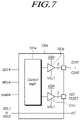
- FIG. 7 is a diagram illustrating the level shifter illustrated in FIG. 3 according to embodiments of the present disclosure.
- the level shifter 130a can include a control logic 131a, a clock signal generator 131b, and a control signal generator 131c.
- the control logic 131a can receive a first clock GCLK and a second clock MCLK, and control the operations of the clock signal generator 131b and the control signal generator 131c.
- the clock signal generator 131b can output a high voltage VGH and a first low voltage VGL1 to a plurality of clock signals (CLK1,...,CLK6) according to the controlling of the control logic 131a.
- Six clock signals (CLK1,...,CLK6) outputted from the clock signal generator 131b is illustrated in FIG. 7 , but embodiments of the present disclosure are not limited thereto and any number of clock signals are possible.
- the control signal generator 131c can output a control signal VST or RESET for controlling the gate signal generating circuit 130b.
- the gate signal generating circuit 130b can output a gate signal (gate) in the first mode and a gate signal (gate) in the second mode, using the clock signal (CLK1,...,CLK6) and the direct current (DC) signal.
- the level shifter 130a can receive one of the first low voltage VGL1 or the second low voltage VGL2 and output the direct current (DC) signal corresponding to the received first low voltage VGL1 or second low voltage VGL2.
- DC direct current
- FIG. 8 is a circuit diagram illustrating a current sensor connected to one of the subpixels of the display panel 110, which may have the configuration as illustrated in FIG. 2 , according to embodiments of the present disclosure.
- the current sensor 160 can include an integrator.
- the integrator 160 can include an amplifier 161, a capacitor C, a switch SW1, a resistor R, and the like.
- the (-) terminal and the (+) terminal of the amplifier 161 can be connected to the resistor R and a reference signal ref1, respectively.
- a sampling switch SAM can be connected to the second electrode of the third transistor M3 of the subpixel 101.
- the third transistor M3 may be turned on by a sensing control signal (Sense). Current may flow from the third node N3 to the second power supply line VL2 through the third transistor M3; therefore, a voltage is formed in the second power supply line VL2.
- the sampling switch (SAM) may be connected to the second power supply line VL2. When a certain time has elapsed, the sampling switch (SAM) becomes turned on.
- the sampling switch SAM
- the characteristic value of the subpixel 101 can be sensed depending on a magnitude of the current.
- the capacitor C may be reset by the switch SW1.
- the capacitor C is operated in the first mode; therefore, it is much affected by a noise in the first mode. Accordingly, in order for the capacitor C not to be affected by the noise, the gate signal may have the waveform in FIG. 5B .
- a voltage outputted by the current sensor 160 may decrease according to the current inputted to the current sensor 160, as shown in FIG. 9 .
- a rate at which the voltage decreases is slow as in (a) of FIG. 9
- the rate is fast as in (b) when the amount of current is large.
- the current sensor 160 may be incorporated partially within the data driver 120. However, embodiments of the present disclosure are not limited thereto, and other configurations are possible.
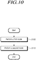
- FIG. 10 is a flow diagram illustrating a method of driving the organic light emitting display device according to embodiments of the present disclosure.
- a method of driving the organic light emitting display device can include supplying a sensing voltage to the subpixel in response to a gate signal in a first mode, at step S100.
- the method can further include receiving a pulse signal or clock signal with a voltage level between a high voltage and a first low voltage, and a direct current (DC) signal corresponding to a voltage level of a second low voltage, and outputting a gate signal.
- a pulse signal or clock signal with a voltage level between a high voltage and a first low voltage
- DC direct current
- the method can include outputting a data voltage to the subpixel in response to the gate signal in a second mode, at step S110.
- the method can further include receiving the clock signal with the voltage level between the high voltage and the first low voltage, and a direct current (DC) signal corresponding to a voltage level of the first low voltage, and outputting a gate signal.
- DC direct current
- the first mode may be a time where the organic light emitting display device starts its operation. That is, when a user starts to use the organic light emitting display device, the first mode is first performed, and then the second mode is performed and continues until the using of the organic light emitting display device by the user is completed. In other words, a data signal is revised according to the characteristic value of the subpixel that is sensed in the first mode, and then the second mode is performed based on the revised data signal.
- characteristics of the first transistor can be sensed, such as electron mobility and a threshold voltage of the first transistor.
- embodiments of the present disclosure are not limited thereto and other characteristic values can be sensed.
- the first mode may be performed for each frame in images including a plurality of frames.
- the first mode can be performed, and a characteristic value of a subpixel can be sensed by a sensing signal. Thereafter, a data signal corresponding to the frame can be inputted, resulting in the second mode being performed. Accordingly, the first mode and the second mode can be repeated alternately.
- the data signal can be revised according to a characteristic value of a subpixel for each frame, before applying the same to the subpixel.
- electron mobility and a threshold voltage of the first transistor can be sensed.
- embodiments of the present disclosure are not limited thereto, and different characteristic values can be sensed.
Landscapes
- Engineering & Computer Science (AREA)
- Theoretical Computer Science (AREA)
- Physics & Mathematics (AREA)
- General Physics & Mathematics (AREA)
- Computer Hardware Design (AREA)
- General Engineering & Computer Science (AREA)
- Control Of Indicators Other Than Cathode Ray Tubes (AREA)
- Control Of El Displays (AREA)
- Electroluminescent Light Sources (AREA)
Abstract
Description
- This application claims the priority benefit of
Korean Patent Application No. 10-2018-0101931, filed on August 29, 2018 - The present disclosure relates to gate drivers, organic light emitting display devices including the same and methods of driving the gate drivers and organic light emitting display devices.
- As the information society has developed at a rapid rate, there is an increasing need for display devices employing advanced technologies and more efficient methods. Recently, various types of flat display devices, such as a liquid crystal display (LCD) device, a plasma display panel (PDP) device, an organic light emitting display (OLED) device, or the like, have been developed and utilized.
- Among the flat display devices, the organic light emitting display device has advantageous to a thinner display device, and has better viewing angles, a higher contrast ratio and the like. Accordingly, the organic light emitting display device has been widely used in various types of devices. The organic light emitting display device emits light and displays images by supplying driving currents to one or more organic light emitting diodes capable of directly illuminating each pixel. However, the light emitting performance of the organic light emitting diode may not remain constant indefinitely. As the organic light emitting diode ages over time and use, it may be degraded, and when displaying still images with a high luminance, it may be further degraded. The organic light emitting diode may have a problem that an undesired after-image can be perceived due to the degradation; therefore, its lifetime can be shortened.
- Furthermore, threshold voltages of driving transistors supplying driving voltages to the organic light emitting diode may change due to process variations; as a result, there is a possibility that a difference in driving currents between subpixels occurs. When a difference in the driving currents occurs, the luminance of the organic light emitting diodes may not be uniform across the display; therefore, there is a possibility that the quality of displayed images reduces. When the organic light emitting diode is degraded, there is a possibility that it emits light at luminance lower than a gray scale voltage.
- Accordingly, in order to prevent display quality from being reduced, the organic light emitting device can be operated in a sensing mode for sensing characteristics of a display panel and in a display mode for revising data signals based on sensed results, and displaying images using the revised data signals.
- Furthermore, in the case of an active matrix type of organic light emitting display device, data signals can be applied to subpixels in response to gate signals; therefore, light corresponding to the data signals can be emitted from the subpixels. However, in the case of organic light emitting display devices with a large area and a higher resolution, resistance-capacitance (RC) delay may increase; therefore a gate signal may be delayed. The delay of the gate signal may result in a data signal corresponding to an intended subpixel being applied to a data signal corresponding to another subpixel; therefore, there is a possibility that the quality of displayed images may reduce.
- Accordingly, the present disclosure is directed to gate drivers, organic light emitting display devices and methods of driving the gate drivers and the organic light emitting display devices that substantially obviate one or more problems due to limitations and disadvantages of the prior art.
- It is at least one object of the present disclosure to provide gate drivers and organic light emitting display devices capable of preventing display quality from being reduced, and methods of driving the gate drivers and the organic light emitting display devices.
- It is at least one object of the present disclosure to provide gate drivers and organic light emitting display devices capable of preventing a gate signal from being delayed due to RC delay, and methods of driving the gate drivers and the organic light emitting display devices.
- It is at least one object of the present disclosure to provide gate drivers and organic light emitting display devices with a large area and a higher resolution, and methods of driving the gate drivers and the organic light emitting display devices.
- The objects are solved by the features of the independent claims. In accordance with one aspect of the present disclosure, a gate driver, in particular for an organic light emitting display device, includes: a selector receiving a first low voltage and a second low voltage with a lower level than the first low voltage, and selecting and outputting one of the first low voltage and the second low voltage such that in response to a mode selection signal, the first low voltage is selected in a first mode and the second low voltage is selected in a second mode, and a level shifter including a first output terminal receiving a high voltage and the first low voltage, and outputting a clock signal with a voltage level between the high voltage and the first low voltage, and a second output terminal outputting a direct current (DC) signal corresponding to the first low voltage or the second low voltage selected in the selector.
- In accordance with one aspect of the present disclosure, a gate driver, in particular for an organic light emitting display device, includes: a selector connected to a power supplier for receiving a first low voltage and a second low voltage with a lower level than the first low voltage therefrom, the selector being configured to select and output one of the first low voltage and the second low voltage in response to a mode selection signal, such that the first low voltage is selected in a first mode and the second low voltage is selected in a second mode, and a level shifter being connected to the selector and to the power supplier for receiving a high voltage and the first low voltage, the level shifter being configured to generate a clock signal with a voltage level between the high voltage and the first low voltage, and a direct current (DC) signal corresponding to the first or second low voltage depending on the selection by the selector. The level shifter may be connected to the selector in order to receive the selected one of the first or second low voltage. The first mode may be referred to as sensing mode, the second mode may be referred to as displaying mode.
- The gate driver may further comprise a gate signal generating circuit receiving the clock signal and the direct current signal and outputting a gate signal such that in the first mode, a voltage level of the gate signal repeats the high voltage and the first low voltage, and in the second mode, the voltage level of the gate signal is changed in the order of the high voltage, the second low voltage, the first low voltage and the high voltage.
- The level shifter may further comprise a control logic; a clock signal generator controlled by the control logic and outputting the clock signal using the high voltage and the first low voltage; and a control signal generator controlled by the control logic and controlling the gate signal generating circuit.
- The gate driver may further comprise a timing controller outputting a sensing signal in the first mode and outputting an image signal in the second mode. The mode selection signal may be received from the timing controller.
- In accordance with another aspect of the present disclosure, an organic light emitting device is provided that includes a gate driver according to any one of the herein described embodiments. Thus, thee organic light emitting device may include: a display panel on which a plurality of data lines and a plurality of gate lines intersect, and which includes a plurality of subpixels defined in areas in which the plurality of data lines and the plurality of gate lines intersect, a data driver applying one or more data signals or sensing signals to the data lines, a gate driver applying one or more gate signals to the gate lines, a timing controller controlling the data deliver and the gate driver, a selector receiving a first low voltage and a second low voltage with a lower level than the first low voltage, and selecting and outputting one of the first low voltage and the second low voltage such that in response to a mode selection signal, the first low voltage is selected in a first mode and the second low voltage is selected in a second mode, and a level shifter including a first output terminal receiving a high voltage and the first low voltage, and outputting a clock signal with a voltage level between the high voltage and the first low voltage, and a second output terminal outputting a direct current (DC) signal corresponding to the first low voltage or the second low voltage selected in the selector.
- The gate driver may further comprise a gate signal generating circuit receiving the clock signal and the direct current signal and outputting a gate signal such that in the first mode, a voltage level of the gate signal repeats the high voltage and the first low voltage, and in the second mode, the voltage level of the gate signal is changed in the order of the high voltage, the second low voltage, the first low voltage and the high voltage.
- The gate signal generating circuit may be disposed on the display panel and connected to the plurality of gate lines.
- The level shifter may further comprise a control logic; a clock signal generator controlled by the control logic and outputting the clock signal using the high voltage and the first low voltage; and a control signal generator controlled by the control logic and controlling the gate signal generating circuit.
- The timing controller may be configured to cause the data driver to output at least one sensing voltage corresponding to the at least one sensing signal to at least one data line of the plurality of data lines, in the first mode. The timing controller may be configured to cause the data driver to output at least one data voltage corresponding to the at least one data signal to the at least one data line, in the second mode.
- Each of the plurality of subpixels may comprise a first transistor including a first electrode connected to a first node connected to a first power supply line for delivering a high pixel voltage, a gate electrode connected to a second node, and a second electrode connected to a third node; a second transistor including a first electrode connected to at least one data line of the plurality of data lines, a gate electrode connected to at least one gate line of the plurality of gate lines, and a second electrode connected to the second node; a third transistor including a first electrode connected to the third node, a gate electrode connected to a sensing signal line, and a second electrode connected to a second power supply line for delivering a reference voltage; a capacitor connected between the first node and the third node; and an organic light emitting diode including a first electrode connected to the third node and a second electrode connected to a low voltage.
- The organic light emitting display device may further comprise a current sensor sensing a current flowing through the third node and outputting information according to a characteristic value of at least one subpixel of the plurality of subpixels.
- The current sensor may include an integrator comparing a sensing voltage generated by the current flowing through the third node with a pre-set reference voltage, and outputting the information according to the characteristic value of the at least one subpixel.
- The first mode and the second mode may be repeated alternately.
- The first mode may be performed when the display panel starts to operate.
- In accordance with further another aspect of the present disclosure, a method of driving an organic light emitting device is provided that includes: providing a sensing voltage to a subpixel in response to a gate signal in a first mode, and providing a data voltage to the subpixel in response to the gate signal in a second mode. Here, in the first mode, a voltage level of the gate signal is changed in the order of a first low voltage, a high voltage, a second low voltage, and the first low voltage, and in the second mode, the voltage level of the gate signal repeats the first low voltage and the high voltage.
- The method may further comprise: receiving a pulse signal or clock signal with a voltage level between the high voltage and the first low voltage, and a direct current signal corresponding to a voltage level of the second low voltage, and outputting a gate signal, in the first mode.
- The method may further comprise receiving a pulse signal or clock signal with a voltage level between the high voltage and the first low voltage, and a direct current signal corresponding to a voltage level of the first low voltage, and outputting a gate signal, in the second mode.
- According to another aspect, a method for controlling a gate driver for an organic light emitting display device or for controlling a light emitting display device having a gate driver may include receiving, e.g. by a selector, a first low voltage and a second low voltage with a lower level than the first low voltage, and selecting and outputting one of the first low voltage and the second low voltage such that in response to a mode selection signal, the first low voltage is selected in a first mode and the second low voltage is selected in a second mode, and receiving, e.g. by a first output terminal of a level shifter, a high voltage and the first low voltage, and outputting a clock signal with a voltage level between the high voltage and the first low voltage, and outputting, e.g. by a second output terminal of the level shifter, a direct current (DC) signal corresponding to the selected one of the first low voltage or the second low voltage. The mode selection signal may be provided by a timing controller.
- The method may further comprise in response to receiving the clock signal and the direct current signal, outputting a gate signal such that in the first mode, a voltage level of the gate signal repeats the high voltage and the first low voltage, and in the second mode, the voltage level of the gate signal is changed in the order of the high voltage, the second low voltage, the first low voltage and the high voltage.
- The method may further comprise outputting a sensing signal in the first mode and outputting an image signal in the second mode, e.g. by the timing controller.
- The method may further comprise outputting at least one sensing voltage corresponding to the at least one sensing signal to at least one data line of a plurality of data lines of the organic light emitting display device, in the first mode, and outputting at least one data voltage corresponding to the at least one data signal to the at least one data line, in the second mode.
- The method may further comprise sensing a current flowing through a predetermined node of one of a plurality of subpixels of the organic light emitting device and outputting information according to a characteristic value of said subpixel. The method may further comprise comparing a sensing voltage generated by the current flowing through the predetermined node with a pre-set reference voltage, e.g. before outputting the information according to the characteristic value.
- The first mode and the second mode may be repeated alternately. The first mode may be performed when the organic light emitting display device or a display panel thereof starts to operate.
- In accordance with embodiments of the present disclosure, it is possible to provide an organic light emitting display device capable of improving the quality of displayed images, and a method of driving the organic light emitting display device.
- In accordance with embodiments of the present disclosure, it is possible to provide an organic light emitting display device capable of preventing a gate signal from being delayed due to RC delay, and a method of driving the organic light emitting display device.
- In accordance with embodiments of the present disclosure, it is possible to provide an organic light emitting display device with a large area and a high resolution, and a method of driving the organic light emitting display device.
- Additional features and advantages of the disclosure will be set forth in the description which follows and in part will be apparent from the description, or may be learned by practice of the disclosure. The objectives and other advantages of the disclosure will be realized and attained by the structure particularly pointed out in the written description and claims hereof as well as the appended drawings.
-
-
FIG. 1 is a view schematically illustrating an organic light emitting display device according to embodiments of the present disclosure. -
FIG. 2 is a circuit diagram illustrating the subpixel illustrated inFIG. 1 according to embodiments of the present disclosure. -
FIG. 3 is a diagram illustrating a relationship between the gate driver and the power supplier illustrated inFIG. 1 according to embodiments of the present disclosure. -
FIG. 4 is a diagram illustrating the display panel illustrated inFIG. 1 according to embodiments of the present disclosure. -
FIG. 5A illustrates a waveform of a signal outputted from a level shifter in a first mode according to embodiments of the present disclosure. -
FIG. 5B illustrates a waveform of a gate signal outputted from a gate signal generating circuit in the first mode according to embodiments of the present disclosure. -
FIG. 6A illustrates a waveform of a signal outputted from the level shifter in a second mode according to embodiments of the present disclosure. -
FIG.6B illustrates a waveform of a gate signal outputted from the gate signal generating circuit in the second mode according to embodiments of the present disclosure. -
FIG. 7 is a diagram illustrating the level shifter illustrated inFIG. 3 according to embodiments of the present disclosure. -
FIG. 8 is a circuit diagram illustrating a current sensor connected to the subpixel illustrated inFIG. 2 according to embodiments of the present disclosure. -
FIG. 9 illustrates a current sensed from the current sensor illustrated inFIG. 8 according to embodiments of the present disclosure. -
FIG. 10 is a flow diagram illustrating a method of driving the organic light emitting display device according to embodiments of the present disclosure. - Hereinafter, the present preferred embodiments of the disclosure will be described in detail with reference to the accompanying drawings. In denoting elements of the drawings by reference numerals, the same elements will be referenced by the same reference numerals although the elements are illustrated in different drawings. In the following description of the disclosure, detailed description of known functions and configurations incorporated herein may be omitted when it may make the subject matter of the disclosure rather unclear.
- Terms, such as first, second, A, B, (A), or (B) may be used herein to describe elements of the disclosure. Each of the terms is not used to define essence, order, sequence, or number of an element, but is used merely to distinguish the corresponding element from another element. When it is mentioned that an element is "connected" or "coupled" to another element, it should be interpreted that another element may be "interposed" between the elements or the elements may be "connected" or "coupled" to each other via another element as well as that one element is directly connected or coupled to another element.
-
FIG. 1 is a view schematically illustrating an organic light emitting display device according to embodiments of the present disclosure. - Referring to
FIG. 1 , the organic light emitting display device can include adisplay panel 110, agate driver 120, adata driver 130, atiming controller 140, and apower supplier 150. - The
display panel 110 can include a plurality of gate lines (GL1,...,GLn) and a plurality of data lines (DL1,...,DLm), which intersect each other on thedisplay panel 110 at a predetermined angle. Thedisplay panel 110 can include a plurality ofsubpixels 101 arranged to correspond to areas in which the plurality of gate lines (GL1,...,GLn) and the plurality of data lines (DL1,...,DLm) intersect each other. The plurality of subpixels can include at least one organic light emitting diode and a pixel circuit supplying a driving current to the at least one organic light emitting diode. The pixel circuit is connected to the plurality of gate lines (GL1,...,GLn) and the plurality of data lines (DL1,...,DLm), and can supply the driving current to the at least one organic light emitting diode. Here, inFIG. 1 , the plurality of gate lines (GL1,...,GLn) and the plurality of data lines (DL1,...,DLm) are arranged in thedisplay panel 110. However, embodiments of the present disclosure are not limited thereto and other arrangements are possible. - The
data driver 120 can apply one or more data voltages Vdata corresponding to one or more data signals to the plurality of data lines (DL1,...,DLm). The data voltage may correspond to gray scale. Thedata driver 120 can apply one or more sensing voltages Sdata corresponding to one or more sensing signals to the plurality of data lines (DL1,...,DLm). The sensing voltage may be lower than a threshold voltage of the organic light emitting diode. When the sensing voltage is lower than a threshold voltage of the organic light emitting diode, the organic light emitting diode may not emit light. In this situation, even when the sensing signal is delivered, there is a possibility that a corresponding image may not be displayed on thedisplay panel 110. Further, the sensing signal may have a gray scale voltage corresponding to black. It is noted that asingle data driver 120 is illustrated inFIG. 1 , but embodiments of the present disclosure are not limited thereto. The number of data drivers may be determined according to the size or resolution of thedisplay panel 110. For example, two or more data drivers may be employed. In addition, thedata driver 120 may be implemented as an integrated circuit. - The
gate driver 130 can apply one or more gate signals to the gate lines (GL1,...,DLm). One ormore pixels 101 corresponding to the gate lines (GL1,...,GLn) to which one or more gate signals are applied can receive one or more data signals. Further, thegate driver 130 can transfer a sensing control signal to one ormore subpixels 101. Thesubpixel 101 received the sensing control signal outputted from thegate driver 130 can receive a sensing voltage outputted from thedata driver 120. It is noted that asingle gate driver 130 is illustrated inFIG. 1 , but embodiments of the present disclosure are not limited thereto. The number of data drivers may be determined according to the size or resolution of thedisplay panel 110. For example, two or more gate drivers may be employed. Further, thegate driver 130 can include two gate drivers disposed on both sides of thedisplay panel 110, and one can be connected to one or more odd numbered gate lines of the plurality of gate lines (GL1,...,GLn) and the other can be connected to one or more even numbered gate lines of the plurality of gate lines (GL1,...,GLn). However, embodiments of the present disclosure are not limited thereto, and other configurations are possible. Thegate driver 130 may be implemented as an integrated circuit. - The
timing controller 140 can control thedata driver 120 and thegate driver 130. Further, thetiming controller 140 can transfer a data signal and a sensing signal to thedata driver 120. The data signal and the sensing signal may be digital signals. Further, thetiming controller 140 can revise a data signal and transfer the revised signal to thedata driver 120. Herein, operations of thetiming controller 140 are not limited thereto, and other various operations or controlling are possible. Thetiming controller 140 may be implemented as an integrated circuit. Further, thetiming controller 140 can revise a data signal in response to a sensing signal and transfer the revised signal to thedata driver 120. - A
power supplier 150 can supply driving voltages of thedata driver 120, thegate driver 130, and thetiming controller 140. In addition, thepower supplier 150 can supply a driving voltage of thedisplay panel 150. Thepower supplier 150 may be a power management integrated circuit (PMIC) 150. However, embodiments of the present disclosure are not limited thereto, and other configurations are possible. -
FIG. 2 is a circuit diagram illustrating the subpixel illustrated inFIG. 1 according to embodiments of the present disclosure. - Referring to
FIG. 2 , thesubpixel 101 can include an organic light emitting diode (OLED) and a pixel circuit for driving the organic light emitting diode (OLED). The pixel circuit can include a first transistor M1, a second transistor M2, a third transistor M3, and a capacitor CS. - A first electrode of the first transistor M1 can be connected to a first node N1 connected to a first power supply line VL1 for delivering a pixel high voltage EVDD. The gate electrode of the first transistor M1 can be connected to a second node N2, and a second electrode thereof can be connected to a third node N3. The first transistor M1 enables a current to flow from the first node N1 to the third node N3 in response to a voltage delivered to the second node N2. The first electrode and the second electrode of the first transistor M1 may be a drain electrode and a source electrode, respectively. However, embodiments of the present disclosure are not limited thereto, and other configurations are possible.
- The current flowing from the first node N1 to the third node N3 may correspond to
Equation 1 as follows.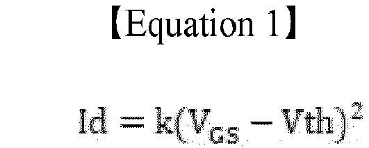
- Here, the Id denotes an amount of current flowing from the first node N1 to the third node N3, the k denotes electron mobility of the transistor, the VGS denotes a difference in voltages between the gate electrode and the source electrode of the first transistor M1, and the Vth denotes a threshold voltage of the first transistor M1.
- Accordingly, since an amount of current varies depending on a deviation in the electron mobility and the threshold voltage; it is therefore possible to prevent the quality of displayed images from being reduced by revising a corresponding data signal in response to the deviation in the electron mobility and the threshold voltage.
- The gate electrode of the second transistor M2 can be connected to a gate line GL, and first and second electrodes thereof can be connected to a data line DL and the second node N2, respectively. Accordingly, the second transistor M2 enables a data voltage Vdata corresponding to the data signal to be delivered to the second node N2 in response to the gate signal delivered through the gate line GL. The first electrode and the second electrode of the second transistor M2 may be a drain electrode and a source electrode, respectively. However, embodiments of the present disclosure are not limited thereto, and other configurations are possible.
- The gate electrode of the third transistor M3 can be connected to a sensing control signal line (Sense), and first and second electrodes thereof can be connected to the third node N3 and a second power supply line VL2 for delivering a reference voltage Vref, respectively. The reference voltage Vref can reset a voltage in the third node N3. In addition, a voltage applied to the third node N3 may include information corresponding to a characteristic value of the
subpixel 101. Accordingly, a data signal may be compensated according to the characteristic value of the subpixel through the voltage applied to the third node N3. In addition, a current flowing through the third node N3 may include information corresponding to the characteristic value of thesubpixel 101. In this situation, the third transistor M3 connected to the third node N3 is connected to a current sensor; therefore, in the current sensor, a current flowing through the third node N3 can be sensed, and the characteristic value of thesubpixel 101 can be detected. The characteristic value of thesubpixel 101 may be a threshold voltage or electron mobility of the first transistor M1, or degradation information of the organic light emitting diode (OLED). However, embodiments of the present disclosure are not limited thereto, and other characteristic values are possible. The first electrode and the second electrode of the third transistor M3 may be a drain electrode and a source electrode, respectively. However, embodiments of the present disclosure are not limited thereto, and other configurations are possible. - The capacitor CS can be connected between the second node N2 and the third node N3. The capacitor CS may constantly maintain voltages in the gate electrode and the source electrode of the first transistor M1.
- The anode electrode and the cathode electrode of the organic light emitting diode (OLED) can be connected to the third node N3 and a pixel low voltage EVSS, respectively. Here, the pixel low voltage EVSS may be a ground voltage. However, embodiments of the present disclosure are not limited thereto, and other voltages are possible. When current flows from the anode electrode to the cathode electrode, the organic light emitting diode (OLED) can emit light depending on an amount of the current. The organic light emitting diode (OLED) can emit light of any one of red, green, blue, and white. However, embodiments of the present disclosure are not limited thereto, and emitting light of other colors is possible.
- A subpixel to be employed in the organic light emitting
display device 100 is not limited to thesubpixel 101 described above. -
FIG. 3 is a diagram illustrating a relationship between the gate driver and the power supplier illustrated inFIG. 1 according to embodiments of the present disclosure. - Referring to
FIG. 3 , thegate driver 130 can operate by a power from thepower supplier 150. Thegate driver 130 can include aselector 130c and alevel shifter 130a. - The
selector 130c can receive a first low voltage VGL1 and a second low voltage VGL2 with a lower level than the first low voltage VGL1, and select and output one of the first low voltage VGL1 and the second low voltage VGL2 such that in response to a mode selection signal, the first low voltage is selected in a first mode and the second low voltage is selected in a second mode. Theselector 130c may be a multiplexer. Theselector 130c can receive the mode selection signal from thetiming controller 140. Thetiming controller 140 can cause thedata driver 120 to output a sensing signal to thesubpixel 101 in the first mode, and cause thedata driver 120 to output a data signal to thesubpixel 101 in the second mode. The first mode may be a mode for sensing a characteristic value of thesubpixel 101, and the sensing mode may be a mode for driving thesubpixel 101 and displaying images on the display panel. Thetiming controller 140 shown inFIG. 1 can cause thedata driver 120 to output a sensing voltage corresponding to the sensing signal to a data line in the first mode, and cause the data driver 120 a data voltage corresponding to the data signal to the data line in the second mode. - The
level shifter 130a can include a first output terminal receiving a high voltage VGH and the first low voltage VGL1, and outputting a clock signal CLKs with a voltage level between the high voltage VGH and the first low voltage VGL1, and a second output terminal outputting a direct current (DC) signal corresponding to the first low voltage VGL1 or the second low voltage VGL2 selected in theselector 130c. Here,FIG. 3 shows that the high voltage VGH, the first low voltage VGL1 and/or the second low voltage VGL2 are applied to thelevel shifter 130a; however, signals and voltages applied to thelevel shifter 130a are not limited thereto. For example, one or more other signals and voltages can be applied to thelevel shifter 130a. - The
gate driver 130 can include a gatesignal generating circuit 130b outputting a gate signal (gate). The gatesignal generating circuit 130b can receive the clock signal CLKs and the direct current (DC) signal and output the gate signal (gate). Here, in the first mode, a voltage level of the gate signal (gate) is changed in the order of the high voltage VGH, the second low voltage VGL2, the first low voltage VGL1, and the high voltage VGH, and in the second mode, the voltage level of the gate signal (gate) repeats the high voltage VGH and the first low voltage VGL1. - The gate
signal generating circuit 130b can output the gate signal (gate) using the clock signal repeating a high state and a low state such that a voltage level in the low state in a falling interval of the clock signal CLKs corresponds to a voltage of the direct current (DC) signal. That is, when the voltage level of the direct current (DC) signal corresponds to the first low voltage VGL1, the voltage level in the high state of the gate signal (gate) can be the high voltage VGH, and the voltage level in the low state thereof can be the first low voltage VGL1. Further, when the voltage level of the direct current (DC) signal corresponds to the second low voltage VGL2, the voltage level in the high state of the gate signal (gate) can be the high voltage VGH, and the low state of the gate signal (gate) can include the first low voltage VGL1 and the second low voltage VGL2 such that the gate signal (gate) first becomes the second low voltage VGL2 for a certain time in the falling interval and thereafter, becomes the first low voltage VGL1 by the rising of the voltage level. - The
gate driver 130 can receive the high voltage VGH, the first low voltage VGL1, and the second low voltage VGL2 from thepower supplier 150. Thepower supplier 150 can generate the high voltage VGH and the first low voltage VGL1 and transfer these to thelevel shifter 130a. Further, thepower supplier 150 can transfer the second low voltage VGL2 different from the first low voltage VGL1 to theselector 130c. However, embodiments of the present disclosure are not limited thereto, and other configurations are possible. -
FIG. 4 is a diagram illustrating the display panel illustrated inFIG. 1 according to embodiments of the present disclosure. - Referring to
FIG. 4 , thedisplay panel 110 can include adisplay area 110a and one or morenon-display areas sides display area 110a, such as left and right sides or top and bottom sides. However, embodiments of the present disclosure are not limited thereto, and the non-display area can be disposed in other one or more areas. The gatesignal generating circuit 130b shown inFIG. 3 can be disposed in thenon-display area signal generating circuit 130b can be formed in conjunction with thedisplay panel 110; therefore, a related manufacturing process can be simplified. -
FIG. 5A illustrates a waveform of a signal outputted from the level shifter in the first mode according to embodiments of the present disclosure, i.e. sensing mode. - Referring to
FIG. 5A , thelevel shifter 130a can receive a high voltage VGH and a first low voltage VGL1 and output a clock signal CLK. The clock signal CLK outputted from thelevel shifter 130a may have a voltage level between the high voltage VGH and the first low voltage VGL1. Voltage levels of the high voltage VGH and the first low voltage VGL1 may be 24V and (-)6V, respectively. However, embodiments of the present disclosure are not limited thereto, and different voltage values are possible. In addition, thelevel shifter 130a can output a direct current (DC) signal. A voltage level of the direct current (DC) signal may be the first low voltage VGL1 selected in theselector 130c. -
FIG. 5B illustrates a waveform of a gate signal outputted from the gate signal generating circuit in the first mode according to embodiments of the present disclosure. - Referring to
FIG. 5B , the first mode may be a mode for sensing a characteristic value of thesubpixel 101. - In the first mode, the gate
signal generating circuit 130b can generate a gate signal using a high voltage VGH and a first low voltage VGL1 received from thelevel shifter 130a. The gate signal (gate) has a voltage of a direct current (DC) signal in a falling interval, and since the voltage of the direct current (DC) signal has the voltage level of the first low voltage VGL1, the gate signal (gate) repeats the high voltage VGH level and the first low voltage VGL1 level. When sensing a characteristic value of thesubpixel 101 using current sensing in the sensing mode, since a capacitance formed inside of thedata driver 120 is used, it is sensitive to a noise outside thereof. The sensing signal becomes coupled to a voltage level of the gate signal (gate); therefore a sensing noise may occur. In this situation, when the voltage level of the gate signal (gate) falls to the voltage level of the second low voltage VGL2 and then rises and reaches the voltage level of the first low voltage VGL1, it may be considered as a noise; thus related sensing data may be different from desired data. However, when the voltage level of the gate signal (gate) repeats the voltage level of the high voltage VGH and the voltage level of the low voltage VGL1, it is possible to prevent the sensing data from being different from desired data due to the noise. -
FIG. 6A illustrates a waveform of a signal outputted from the level shifter in the second mode according to embodiments of the present disclosure, i.e. to the display mode. - Referring to
FIG. 6A , thelevel shifter 130a can receive a high voltage VGH and a first low voltage VGL1 and output a clock signal CLK. The clock signal CLK outputted from thelevel shifter 130a may have a voltage level between the high voltage VGH and the first low voltage VGL1. In addition, thelevel shifter 130a can output a direct current (DC) signal. A voltage level of the direct current (DC) signal may be a second low voltage VGL2 selected in theselector 130c. Voltage levels of the high voltage VGH, the first low voltage VGL1, and the second low voltage VGL2 may be 24V, (-)6V, and (-)18V, respectively. However, embodiments of the present disclosure are not limited thereto, and different voltage values are possible. -
FIG.6B illustrates a waveform of a gate signal outputted from the gate signal generating circuit in the second mode according to embodiments of the present disclosure. - Referring to
FIG. 6B , the second mode may be a display mode for displaying images through light-emitting of thesubpixel 101. - In the second mode, the gate
signal generating circuit 130b can generate a gate signal (gate) using a high voltage VGH, a first low voltage VGL1, and a second low voltage VGL2 received from thelevel shifter 130a. The gate signal (gate) falls up to the direct current (DC) signal in a falling interval where the voltage falls. Since the voltage of the direct current (DC) signal has the voltage level of the second low voltage VGL2, the gate signal (gate) falls from the high voltage VGH level up to the second low voltage VGL2 level in the falling interval, and thereafter, rises and reaches the first low voltage VGL1. That is, in the second mode, current is required to flow through the organic light emitting diode (OLED), rather than performing current sensing; therefore, a situation in the second mode is less affected by external noises than that in the first mode. - Here, the
display panel 110 causes a data voltage corresponding to a data signal to be applied to thesubpixel 101 in a turn-on interval of the gate signal (gate); therefore, causes light corresponding to a data signal to emit from eachsubpixel 101 and a corresponding image to be displayed. In the case of thedisplay panel 110 with a large area and a high resolution, RC delay can increase; therefore, the entering of the gate signal (gate) into a turn-off interval can be delayed. When the turn-off of the gate signal (gate) is delayed, there is a possibility that data signals are mismatched to intendedsubpixels 101. To solve or address such a problem, by reducing the falling interval of the gate signal (gate) and allowing the gate signal (gate) to enter rapidly the turn-off interval, it is possible to prevent data signals from being mismatched to intendedsubpixels 101. In the falling interval, the greater a difference in voltages in the high and low states is, the shorter the falling interval becomes; therefore, the gate signal (gate) can enter the turn-off interval rapidly. Furthermore, it is possible to prevent power consumption from being increased by not allowing a voltage in the high state to be a certain high level. Summarizing, in the second mode, the display process is less sensitive to noise, but an RC delay should be prevented. Therefore, a gate signal having three levels is used in order to increase the difference between the highest voltage level and the lowest voltage level, and thus to rapidly change between the two voltage levels. In contrast, in the first mode, the sensing process is very sensitive to noise, so that a gate signal having three levels would be disadvantageous, while an RC delay is not so important. Therefore, a two-level gate signal is used during the sensing mode. -
FIG. 7 is a diagram illustrating the level shifter illustrated inFIG. 3 according to embodiments of the present disclosure. - Referring to
FIG. 7 , thelevel shifter 130a can include acontrol logic 131a, aclock signal generator 131b, and acontrol signal generator 131c. Thecontrol logic 131a can receive a first clock GCLK and a second clock MCLK, and control the operations of theclock signal generator 131b and thecontrol signal generator 131c. Theclock signal generator 131b can output a high voltage VGH and a first low voltage VGL1 to a plurality of clock signals (CLK1,...,CLK6) according to the controlling of thecontrol logic 131a. Six clock signals (CLK1,...,CLK6) outputted from theclock signal generator 131b is illustrated inFIG. 7 , but embodiments of the present disclosure are not limited thereto and any number of clock signals are possible. Thecontrol signal generator 131c can output a control signal VST or RESET for controlling the gatesignal generating circuit 130b. By the control signal VST or RESET outputted from thecontrol signal generator 131c, the gatesignal generating circuit 130b can output a gate signal (gate) in the first mode and a gate signal (gate) in the second mode, using the clock signal (CLK1,...,CLK6) and the direct current (DC) signal. - Furthermore, the
level shifter 130a can receive one of the first low voltage VGL1 or the second low voltage VGL2 and output the direct current (DC) signal corresponding to the received first low voltage VGL1 or second low voltage VGL2. -
FIG. 8 is a circuit diagram illustrating a current sensor connected to one of the subpixels of thedisplay panel 110, which may have the configuration as illustrated inFIG. 2 , according to embodiments of the present disclosure. - Referring to
FIG. 8 , thecurrent sensor 160 can include an integrator. Theintegrator 160 can include anamplifier 161, a capacitor C, a switch SW1, a resistor R, and the like. The (-) terminal and the (+) terminal of theamplifier 161 can be connected to the resistor R and a reference signal ref1, respectively. A sampling switch SAM can be connected to the second electrode of the third transistor M3 of thesubpixel 101. In the first mode, the third transistor M3 may be turned on by a sensing control signal (Sense). Current may flow from the third node N3 to the second power supply line VL2 through the third transistor M3; therefore, a voltage is formed in the second power supply line VL2. The sampling switch (SAM) may be connected to the second power supply line VL2. When a certain time has elapsed, the sampling switch (SAM) becomes turned on. - When the sampling switch (SAM) becomes turned on, current flows through the
current sensor 160, and the characteristic value of thesubpixel 101 can be sensed depending on a magnitude of the current. The capacitor C may be reset by the switch SW1. The capacitor C is operated in the first mode; therefore, it is much affected by a noise in the first mode. Accordingly, in order for the capacitor C not to be affected by the noise, the gate signal may have the waveform inFIG. 5B . - Further, a voltage outputted by the
current sensor 160 may decrease according to the current inputted to thecurrent sensor 160, as shown inFIG. 9 . Here, when an amount of current is small, a rate at which the voltage decreases is slow as in (a) ofFIG. 9 , while the rate is fast as in (b) when the amount of current is large. Using this relationship, it is possible to obtain information on the characteristic value of thesubpixel 101. - The
current sensor 160 may be incorporated partially within thedata driver 120. However, embodiments of the present disclosure are not limited thereto, and other configurations are possible. -
FIG. 10 is a flow diagram illustrating a method of driving the organic light emitting display device according to embodiments of the present disclosure. - Referring to
FIG, 10 , a method of driving the organic light emitting display device can include supplying a sensing voltage to the subpixel in response to a gate signal in a first mode, at step S100. In the first mode, the method can further include receiving a pulse signal or clock signal with a voltage level between a high voltage and a first low voltage, and a direct current (DC) signal corresponding to a voltage level of a second low voltage, and outputting a gate signal. - The method can include outputting a data voltage to the subpixel in response to the gate signal in a second mode, at step S110. In the second mode, the method can further include receiving the clock signal with the voltage level between the high voltage and the first low voltage, and a direct current (DC) signal corresponding to a voltage level of the first low voltage, and outputting a gate signal.
- The first mode may be a time where the organic light emitting display device starts its operation. That is, when a user starts to use the organic light emitting display device, the first mode is first performed, and then the second mode is performed and continues until the using of the organic light emitting display device by the user is completed. In other words, a data signal is revised according to the characteristic value of the subpixel that is sensed in the first mode, and then the second mode is performed based on the revised data signal. In the first mode, characteristics of the first transistor can be sensed, such as electron mobility and a threshold voltage of the first transistor. However, embodiments of the present disclosure are not limited thereto and other characteristic values can be sensed.
- Additionally or alternatively, the first mode may be performed for each frame in images including a plurality of frames. When one frame is started, before a data signal is applied, the first mode can be performed, and a characteristic value of a subpixel can be sensed by a sensing signal. Thereafter, a data signal corresponding to the frame can be inputted, resulting in the second mode being performed. Accordingly, the first mode and the second mode can be repeated alternately. The data signal can be revised according to a characteristic value of a subpixel for each frame, before applying the same to the subpixel. Thus, in the first mode, electron mobility and a threshold voltage of the first transistor can be sensed. However, embodiments of the present disclosure are not limited thereto, and different characteristic values can be sensed.
- The features, structures, configurations, and effects described in the present disclosure are included in at least one embodiment but are not necessarily limited to a particular embodiment. A person skilled in the art can apply the features, structures, configurations, and effects illustrated in the particular embodiment embodiments to one or more other additional embodiment embodiments by combining or modifying such features, structures, configurations, and effects. It should be understood that all such combinations and modifications are included within the scope of the present disclosure Although the exemplary embodiments have been described for illustrative purposes, a person skilled in the art will appreciate that various modifications and applications are possible without departing from the essential characteristics of the present disclosure. For example, the specific components of the exemplary embodiments may be variously modified. The scope of protection of the present disclosure should be construed based on the following claims, and all technical ideas within the scope of equivalents thereof should be construed as being included within the scope of the present disclosure.
-
- 1. A gate driver for an organic light emitting display device comprising:
- a selector (130c) configured to select and output one of a first low voltage (VGL1) and a second low voltage (VGL2) in response to a mode selection signal, the second low voltage (VGL2) having a lower level than the first low voltage (VGL1), wherein the first low voltage (VGL1) is selected in a first mode and the second low voltage (VGL2) is selected in a second mode, and
- a level shifter (130a) configured to generate a clock signal (CLKs) based on a high voltage (VGH) and the first low voltage (VGL1), the high voltage (VGH) having a voltage level higher than the first low voltage (VGL1) and the clock signal (CLKs) having a voltage level between the high voltage (VGH) and the first low voltage (VGL1), and to output the clock signal (CLKs) at a first output terminal, the level shifter (130a) being further configured to generate a direct current signal (DC) corresponding to the first or second low voltage (VGL1, VGL2) outputted from the selector (130c) and to output the direct current signal (DC) at a second output terminal.
- 2. The gate driver according to example 1, further comprising a gate signal generating circuit (130b) connected to the level shifter (130a) to receive the clock signal (CLKs) and the direct current signal (DC) and configured to output a gate signal (gate) such that in the first mode, a voltage level of the gate signal (gate) repeatedly alternates between the high voltage (VGH) and the first low voltage (VGL1), and in the second mode, the voltage level of the gate signal (gate) is repeatedly changed in the order of the high voltage (VGH), the second low voltage (VGL2), and the first low voltage (VGL1).
- 3. The gate driver according to example 2, wherein the level shifter (130a) further comprises:
a control logic (131a);- a clock signal generator (131b) controlled by the control logic (131a) and configured to generate and output the clock signal (CLKs); and
- a control signal generator (131c) controlled by the control logic (131a) and configured to output a control signal (VST RESET) for controlling the gate signal generating circuit (130b).
- 4. An organic light emitting display device comprising:
- a display panel (110) including a plurality of data lines (DL) and a plurality of gate lines (GL) and a plurality of subpixels (101) defined in areas in which the plurality of data lines (DL) and the plurality of gate lines (GL) intersect;
- a data driver (120) configured to apply at least one of a data signal or a sensing signal to the data lines (DL);
- a gate driver (130) according to any one of the preceding claims, the gate driver (130) being configured to apply a gate signal (gate) to the gate lines (GL); and
- a timing controller (140) configured to control the data driver (120) and the gate driver (130).
- 5. The organic light emitting display device according to example 4 when depending on
claim 2, wherein the gate signal generating circuit (130b) is disposed on the display panel (110) and connected to the plurality of gate lines (GL). - 6. The organic light emitting display device according to example 4 or 5, wherein the timing controller (140) is configured to control the data driver (12) to output at least one sensing voltage (Sdata) corresponding to the at least one sensing signal to at least one data line (DL) of the plurality of data lines, in the first mode, and to control the data driver (140) to output at least one data voltage (Vdata) corresponding to the at least one data signal to the at least one data line (DL), in the second mode.
- 7. The gate driver according to example 4, 5 or 6, wherein the timing controller (140) is configured to output the mode selection signal, a sensing signal in the first mode and an image signal in the second mode.
- 8. The organic light emitting display device according to any one of examples 4 to 7, wherein each of the plurality of subpixels (101) comprises:
- a first transistor (M1) including a first electrode connected to a first node (N1) connected to a first power supply line (VL1) for delivering a pixel high voltage (EVDD), a gate electrode connected to a second node (N2), and a second electrode connected to a third node (N3);
- a second transistor (M2) including a first electrode connected to one data line (DL) of the plurality of data lines, a gate electrode connected to one gate line (GL) of the plurality of gate lines, and a second electrode connected to the second node (N2);
- a third transistor (M3) including a first electrode connected to the third node (N3), a gate electrode connected to a sensing signal line (sense), and a second electrode connected to a second power supply line (VL2) for delivering a reference voltage (Vref);
- a capacitor (Cs) connected between the first node (N1) and the third node (N3); and
- an organic light emitting diode (OLED) including a first electrode connected to the third node (N3) and a second electrode connected to a pixel low voltage (EVSS).
- 9. The organic light emitting display device according to example 8, further comprising a current sensor (160) connected to the second electrode of the third transistor (M3) and configured to sense a current flowing through the third node (N3) and output information according to a characteristic value of the corresponding subpixel (101).
- 10. The organic light emitting display device according to example 9, wherein the current sensor (160) includes an integrator (161) comparing a sensing voltage generated by the current flowing through the third node (N3) with a pre-set reference voltage (Vref), and outputting the information according to the characteristic value of corresponding subpixel (101).
- 11. A method for controlling a gate driver for an organic light emitting display device including:
- receiving a first low voltage (VGL1) and a second low voltage (VGL2) with a lower level than the first low voltage (VGL1) and a high voltage (VGH) with a higher level than the first low voltage (VGL1) and a mode selection signal,
- selecting and outputting one of the first low voltage (VGL1) and the second low voltage (VGL2) in response to the mode selection signal, wherein the first low voltage (VGL1) is selected in a first mode and the second low voltage (VGL2) is selected in a second mode,
- outputting a clock signal (CLKs) with a voltage level between the high voltage (VGH) and the first low voltage (VGL1) and a direct current signal (DC) corresponding to the selected one of the first and second low voltage (VGL1, VGL2).
- 12. The method further comprising:
- providing a sensing voltage (Sdata) to a subpixel (101) in response to a gate signal in a first mode; and
- providing a data voltage (Vdata) to the subpixel (101) in response to the gate signal in a second mode,
- wherein in the second mode, a voltage level of the gate signal is repeatedly changed in the order of a first low voltage (VGL1), a high voltage (VGH), and a second low voltage (VGL2), and
- in the first mode, the voltage level of the gate signal is repeatedly changed the first low voltage (VGL1) and the high voltage (VGH).
- 13. The method according to example 12 or 13, wherein the direct current signal (DC) has a voltage level corresponding to the voltage level of the first low voltage (VGL1) in the first mode, and a voltage level corresponding to the voltage level of the second low voltage (VGL2) in the second mode.
- 14. The organic light emitting display device according to any one of examples 11 to 13, wherein the first mode is a sensing mode and the second mode is a display mode and the first mode and the second mode are repeated alternately.
- 15. The method according to any one of the preceding examples 11 to 14, wherein the first mode is a sensing mode and the second mode is a display mode and the first mode and the first mode is performed when the display panel (110) starts to operate.
Claims (7)
- A method for driving an organic light emitting display device including:receiving, by a gate driver (130) of the organic light emitting display device, a first low voltage (VGL1), a second low voltage (VGL2) lower than the first low voltage (VGL1), a high voltage (VGH) higher than the first low voltage (VGL1), and a mode selection signal;in a first mode according to the mode selection signal, outputting, by the gate driver (130), a two-level gate signal (gate) alternating between the first low voltage (VGL1) and the high voltage (VGH) to a gate line (GL) in the organic light emitting display device; andin a second mode according to the mode selection signal, outputting, by the gate driver (130), a three-level gate signal (gate) alternating with the first low voltage (VGL1), the high voltage (VGH), and the second low voltage (VGL2) to the gate line (GL) in the organic light emitting display device.
- The method according to Claim 1, further comprising:providing, by a data driver, a sensing voltage (Sdata) to a sub-pixels (101) of the organic light emitting diode display when the two-level gate signal (gate) is output to the gate line (GL) in the first mode; andproviding, by the data driver, a data voltage (Vdata) to the subpixel (101) when the three-level gate signal (gate) is output to the gate line (GL) in the second mode.
- The method according to Claim 2, wherein the pixel includes:a first transistor (M1) including a first electrode connected to a first node (N1) connected to a first power supply line (VL1) for delivering a pixel high voltage (EVDD), a gate electrode connected to a second node (N2), and a second electrode connected to a third node (N3);a second transistor (M2) including a first electrode connected to one data line (DL) of the plurality of data lines, a gate electrode connected to the gate line (GL), and a second electrode connected to the second node (N2);a third transistor (M3) including a first electrode connected to the third node (N3), a gate electrode connected to a sensing signal line (sense), and a second electrode connected to a second power supply line (VL2) for delivering a reference voltage (Vref);a capacitor (Cs) connected between the first node (N1) and the third node (N3); andan organic light emitting diode (OLED) including a first electrode connected to the third node (N3) and a second electrode connected to a pixel low voltage (EVSS).
- The method according to Claim 3, wherein the first mode is a mode for sensing a threshold voltage or electron mobility of the first transistor M1.
- The method according to any one of Claims 1 to 4, wherein the first mode is a sensing mode and the second mode is a display mode.
- The method according to any one of Claims 1 to 5, wherein the first mode and the second mode are repeated alternately.
- The method according to any one of Claims 1 to 6, wherein the first mode is performed when the display panel (110) starts to operate.
Applications Claiming Priority (2)
| Application Number | Priority Date | Filing Date | Title |
|---|---|---|---|
| KR1020180101931A KR102715269B1 (en) | 2018-08-29 | 2018-08-29 | Gate driver, organic light emitting display apparatus and driving method thereof |
| EP19193638.4A EP3618047A1 (en) | 2018-08-29 | 2019-08-26 | Gate driver, organic light emitting display device and driving method thereof |
Related Parent Applications (1)
| Application Number | Title | Priority Date | Filing Date |
|---|---|---|---|
| EP19193638.4A Division EP3618047A1 (en) | 2018-08-29 | 2019-08-26 | Gate driver, organic light emitting display device and driving method thereof |
Publications (1)
| Publication Number | Publication Date |
|---|---|
| EP4109442A1 true EP4109442A1 (en) | 2022-12-28 |
Family
ID=67766103
Family Applications (2)
| Application Number | Title | Priority Date | Filing Date |
|---|---|---|---|
| EP22173013.8A Pending EP4109442A1 (en) | 2018-08-29 | 2019-08-26 | Gate driver, organic light emitting display device and driving method thereof |
| EP19193638.4A Ceased EP3618047A1 (en) | 2018-08-29 | 2019-08-26 | Gate driver, organic light emitting display device and driving method thereof |
Family Applications After (1)
| Application Number | Title | Priority Date | Filing Date |
|---|---|---|---|
| EP19193638.4A Ceased EP3618047A1 (en) | 2018-08-29 | 2019-08-26 | Gate driver, organic light emitting display device and driving method thereof |
Country Status (5)
| Country | Link |
|---|---|
| US (1) | US10847094B2 (en) |
| EP (2) | EP4109442A1 (en) |
| JP (1) | JP6827076B2 (en) |
| KR (1) | KR102715269B1 (en) |
| CN (1) | CN110875010B (en) |
Families Citing this family (8)
| Publication number | Priority date | Publication date | Assignee | Title |
|---|---|---|---|---|
| CN111326113B (en) * | 2018-12-17 | 2022-06-03 | 乐金显示有限公司 | Organic Light Emitting Display Device |
| KR102756227B1 (en) * | 2019-12-27 | 2025-01-17 | 엘지디스플레이 주식회사 | OLED display device and driving method therefor |
| KR102796294B1 (en) * | 2020-07-15 | 2025-04-17 | 삼성디스플레이 주식회사 | Data driver, display apparatus having the same and method of sensing threshold voltage of pixel using the same |
| KR20230148892A (en) | 2022-04-18 | 2023-10-26 | 삼성디스플레이 주식회사 | Pixel and display device having the same |
| KR20230148891A (en) * | 2022-04-18 | 2023-10-26 | 삼성디스플레이 주식회사 | Pixel and display device having the same |
| CN118197198A (en) * | 2022-12-13 | 2024-06-14 | 群创光电股份有限公司 | Electronic Devices |
| US20250157411A1 (en) * | 2023-11-09 | 2025-05-15 | Lg Display Co., Ltd. | Gate driving circuit and display device |
| KR20260047735A (en) * | 2024-10-02 | 2026-04-09 | 엘지디스플레이 주식회사 | Data Driving Circuit, Driving Method of the Data Driving Circuit, and Display Device including the Data Driving Circuit |
Citations (4)
| Publication number | Priority date | Publication date | Assignee | Title |
|---|---|---|---|---|
| US20150255015A1 (en) * | 2012-10-09 | 2015-09-10 | Joled Inc. | Image display apparatus |
| US20150279272A1 (en) * | 2012-10-17 | 2015-10-01 | Joled Inc. | Gate driver integrated circuit, and image display apparatus including the same |
| KR20170081034A (en) * | 2015-12-31 | 2017-07-11 | 엘지디스플레이 주식회사 | Gate driving method, sensing driving method, gate driver, and organic light emitting display device |
| KR20180101931A (en) | 2017-03-06 | 2018-09-14 | 엘에스산전 주식회사 | Monitering and controlling system |
Family Cites Families (15)
| Publication number | Priority date | Publication date | Assignee | Title |
|---|---|---|---|---|
| JP4798342B2 (en) | 2005-03-31 | 2011-10-19 | カシオ計算機株式会社 | Display drive device and drive control method thereof, and display device and drive control method thereof |
| KR101267019B1 (en) * | 2005-10-18 | 2013-05-30 | 삼성디스플레이 주식회사 | Flat panel display |
| KR20070121318A (en) * | 2006-06-22 | 2007-12-27 | 삼성전자주식회사 | LCD and its driving method |
| KR101274710B1 (en) * | 2008-07-10 | 2013-06-12 | 엘지디스플레이 주식회사 | Light emitting diode display |
| BR112012010454A2 (en) * | 2009-11-04 | 2016-03-08 | Sharp Kk | liquid crystal display device and method of actuation thereof. |
| KR101127590B1 (en) * | 2010-03-29 | 2012-03-23 | 삼성모바일디스플레이주식회사 | Active Level Shift Driver Circuit, Liquid Crystal Display Device comprising ALS Driver and Driving method of Liquid Crystal Display Device |
| KR101808338B1 (en) * | 2010-10-21 | 2017-12-13 | 엘지디스플레이 주식회사 | Display device and method of controlling gate pulse thereof |
| CN103703507B (en) * | 2011-08-10 | 2016-04-27 | 夏普株式会社 | Liquid crystal indicator and driving method thereof |
| KR101931335B1 (en) * | 2012-03-23 | 2018-12-20 | 엘지디스플레이 주식회사 | Level shifter for liquid crystal display |
| KR101989931B1 (en) * | 2012-09-20 | 2019-06-17 | 엘지디스플레이 주식회사 | Liquid crystal display and undershoot generation circuit thereof |
| KR20140109675A (en) * | 2013-03-06 | 2014-09-16 | 삼성전자주식회사 | Gate driver and display driving circuit |
| KR101577909B1 (en) * | 2014-09-05 | 2015-12-16 | 엘지디스플레이 주식회사 | Degradation Sensing Method of Organic Light Emitting Display |
| KR102371182B1 (en) * | 2015-06-30 | 2022-03-08 | 엘지디스플레이 주식회사 | Display device, panel defect detection system, and panel defect detection method |
| KR102408698B1 (en) * | 2015-11-05 | 2022-06-14 | 엘지디스플레이 주식회사 | Voltage Controller, Display Device and Method for driving thereof |
| KR102604368B1 (en) | 2016-07-28 | 2023-11-22 | 엘지디스플레이 주식회사 | Organic light emitting display panel, organic light emitting display device, driving circuit, controller, and driving method |
-
2018
- 2018-08-29 KR KR1020180101931A patent/KR102715269B1/en active Active
-
2019
- 2019-08-19 JP JP2019149705A patent/JP6827076B2/en active Active
- 2019-08-19 US US16/543,990 patent/US10847094B2/en active Active
- 2019-08-21 CN CN201910774342.1A patent/CN110875010B/en active Active
- 2019-08-26 EP EP22173013.8A patent/EP4109442A1/en active Pending
- 2019-08-26 EP EP19193638.4A patent/EP3618047A1/en not_active Ceased
Patent Citations (4)
| Publication number | Priority date | Publication date | Assignee | Title |
|---|---|---|---|---|
| US20150255015A1 (en) * | 2012-10-09 | 2015-09-10 | Joled Inc. | Image display apparatus |
| US20150279272A1 (en) * | 2012-10-17 | 2015-10-01 | Joled Inc. | Gate driver integrated circuit, and image display apparatus including the same |
| KR20170081034A (en) * | 2015-12-31 | 2017-07-11 | 엘지디스플레이 주식회사 | Gate driving method, sensing driving method, gate driver, and organic light emitting display device |
| KR20180101931A (en) | 2017-03-06 | 2018-09-14 | 엘에스산전 주식회사 | Monitering and controlling system |
Also Published As
| Publication number | Publication date |
|---|---|
| EP3618047A1 (en) | 2020-03-04 |
| CN110875010B (en) | 2022-07-26 |
| US20200074931A1 (en) | 2020-03-05 |
| JP6827076B2 (en) | 2021-02-10 |
| US10847094B2 (en) | 2020-11-24 |
| KR102715269B1 (en) | 2024-10-10 |
| JP2020034907A (en) | 2020-03-05 |
| CN110875010A (en) | 2020-03-10 |
| KR20200025091A (en) | 2020-03-10 |
Similar Documents
| Publication | Publication Date | Title |
|---|---|---|
| US10847094B2 (en) | Gate driver, organic light emitting display device and driving method thereof | |
| US11790832B2 (en) | Driving signals and driving circuits in display device and driving method thereof | |
| EP3493189B1 (en) | Electroluminescent display device | |
| US7283108B2 (en) | Electro-optical device, method of driving electro-optical device, and electronic apparatus | |
| US9552760B2 (en) | Display panel | |
| EP3680885A1 (en) | Display apparatus and method of driving display panel using the same | |
| US20070285359A1 (en) | Display apparatus | |
| US20170316741A1 (en) | Color display device with pixel circuits including two capacitors | |
| US20140168195A1 (en) | Electro-optic device and driving method thereof | |
| CN102971782B (en) | The driving method of display device and display device | |
| US10692431B2 (en) | Gate driver, display apparatus having the same and method of driving display panel using the same | |
| US7463224B2 (en) | Light emitting device and display device | |
| US20150187252A1 (en) | Driving method of display apparatus and display apparatus | |
| KR20190058087A (en) | Gate driver and electroluminescence display device including the same | |
| EP3675104A1 (en) | Display apparatus and method of driving the same | |
| KR20190064265A (en) | Electroluminescent display device | |
| KR20190064267A (en) | Electroluminescent display device | |
| TWI759067B (en) | Display device and driving method | |
| JP7269439B2 (en) | Display device and its driving method | |
| US9208724B2 (en) | Display device and method of driving the same | |
| JP2008180836A (en) | Display device having partial display function | |
| JP4797555B2 (en) | Display device and driving method thereof | |
| US20040207579A1 (en) | Display device | |
| KR100670332B1 (en) | Organic electroluminescent display and its driving method | |
| US12555544B2 (en) | Gate driving circuit and display device including the same |
Legal Events
| Date | Code | Title | Description |
|---|---|---|---|
| PUAI | Public reference made under article 153(3) epc to a published international application that has entered the european phase |
Free format text: ORIGINAL CODE: 0009012 |
|
| STAA | Information on the status of an ep patent application or granted ep patent |
Free format text: STATUS: REQUEST FOR EXAMINATION WAS MADE |
|
| 17P | Request for examination filed |
Effective date: 20220531 |
|
| AC | Divisional application: reference to earlier application |
Ref document number: 3618047 Country of ref document: EP Kind code of ref document: P |
|
| AK | Designated contracting states |
Kind code of ref document: A1 Designated state(s): AL AT BE BG CH CY CZ DE DK EE ES FI FR GB GR HR HU IE IS IT LI LT LU LV MC MK MT NL NO PL PT RO RS SE SI SK SM TR |
|
| RBV | Designated contracting states (corrected) |
Designated state(s): AL AT BE BG CH CY CZ DE DK EE ES FI FR GB GR HR HU IE IS IT LI LT LU LV MC MK MT NL NO PL PT RO RS SE SI SK SM TR |
|
| STAA | Information on the status of an ep patent application or granted ep patent |
Free format text: STATUS: EXAMINATION IS IN PROGRESS |
|
| 17Q | First examination report despatched |
Effective date: 20250312 |