EP4109338A1 - Rfid tag, and antenna - Google Patents
Rfid tag, and antenna Download PDFInfo
- Publication number
- EP4109338A1 EP4109338A1 EP21756995.3A EP21756995A EP4109338A1 EP 4109338 A1 EP4109338 A1 EP 4109338A1 EP 21756995 A EP21756995 A EP 21756995A EP 4109338 A1 EP4109338 A1 EP 4109338A1
- Authority
- EP
- European Patent Office
- Prior art keywords
- slot
- antenna
- adjustment
- rfid tag
- conductive layer
- Prior art date
- Legal status (The legal status is an assumption and is not a legal conclusion. Google has not performed a legal analysis and makes no representation as to the accuracy of the status listed.)
- Withdrawn
Links
Images






Classifications
-
- H—ELECTRICITY
- H01—ELECTRIC ELEMENTS
- H01Q—ANTENNAS, i.e. RADIO AERIALS
- H01Q1/00—Details of, or arrangements associated with, antennas
- H01Q1/12—Supports; Mounting means
- H01Q1/22—Supports; Mounting means by structural association with other equipment or articles
- H01Q1/2208—Supports; Mounting means by structural association with other equipment or articles associated with components used in interrogation type services, i.e. in systems for information exchange between an interrogator/reader and a tag/transponder, e.g. in Radio Frequency Identification [RFID] systems
- H01Q1/2225—Supports; Mounting means by structural association with other equipment or articles associated with components used in interrogation type services, i.e. in systems for information exchange between an interrogator/reader and a tag/transponder, e.g. in Radio Frequency Identification [RFID] systems used in active tags, i.e. provided with its own power source or in passive tags, i.e. deriving power from RF signal
-
- G—PHYSICS
- G06—COMPUTING OR CALCULATING; COUNTING
- G06K—GRAPHICAL DATA READING; PRESENTATION OF DATA; RECORD CARRIERS; HANDLING RECORD CARRIERS
- G06K19/00—Record carriers for use with machines and with at least a part designed to carry digital markings
- G06K19/06—Record carriers for use with machines and with at least a part designed to carry digital markings characterised by the kind of the digital marking, e.g. shape, nature, code
- G06K19/067—Record carriers with conductive marks, printed circuits or semiconductor circuit elements, e.g. credit or identity cards also with resonating or responding marks without active components
- G06K19/07—Record carriers with conductive marks, printed circuits or semiconductor circuit elements, e.g. credit or identity cards also with resonating or responding marks without active components with integrated circuit chips
- G06K19/077—Constructional details, e.g. mounting of circuits in the carrier
- G06K19/07749—Constructional details, e.g. mounting of circuits in the carrier the record carrier being capable of non-contact communication, e.g. constructional details of the antenna of a non-contact smart card
- G06K19/0775—Constructional details, e.g. mounting of circuits in the carrier the record carrier being capable of non-contact communication, e.g. constructional details of the antenna of a non-contact smart card arrangements for connecting the integrated circuit to the antenna
- G06K19/07754—Constructional details, e.g. mounting of circuits in the carrier the record carrier being capable of non-contact communication, e.g. constructional details of the antenna of a non-contact smart card arrangements for connecting the integrated circuit to the antenna the connection being galvanic
-
- G—PHYSICS
- G06—COMPUTING OR CALCULATING; COUNTING
- G06K—GRAPHICAL DATA READING; PRESENTATION OF DATA; RECORD CARRIERS; HANDLING RECORD CARRIERS
- G06K19/00—Record carriers for use with machines and with at least a part designed to carry digital markings
- G06K19/06—Record carriers for use with machines and with at least a part designed to carry digital markings characterised by the kind of the digital marking, e.g. shape, nature, code
- G06K19/067—Record carriers with conductive marks, printed circuits or semiconductor circuit elements, e.g. credit or identity cards also with resonating or responding marks without active components
- G06K19/07—Record carriers with conductive marks, printed circuits or semiconductor circuit elements, e.g. credit or identity cards also with resonating or responding marks without active components with integrated circuit chips
- G06K19/077—Constructional details, e.g. mounting of circuits in the carrier
- G06K19/07749—Constructional details, e.g. mounting of circuits in the carrier the record carrier being capable of non-contact communication, e.g. constructional details of the antenna of a non-contact smart card
- G06K19/07773—Antenna details
-
- G—PHYSICS
- G06—COMPUTING OR CALCULATING; COUNTING
- G06K—GRAPHICAL DATA READING; PRESENTATION OF DATA; RECORD CARRIERS; HANDLING RECORD CARRIERS
- G06K19/00—Record carriers for use with machines and with at least a part designed to carry digital markings
- G06K19/06—Record carriers for use with machines and with at least a part designed to carry digital markings characterised by the kind of the digital marking, e.g. shape, nature, code
- G06K19/067—Record carriers with conductive marks, printed circuits or semiconductor circuit elements, e.g. credit or identity cards also with resonating or responding marks without active components
- G06K19/07—Record carriers with conductive marks, printed circuits or semiconductor circuit elements, e.g. credit or identity cards also with resonating or responding marks without active components with integrated circuit chips
- G06K19/077—Constructional details, e.g. mounting of circuits in the carrier
- G06K19/07749—Constructional details, e.g. mounting of circuits in the carrier the record carrier being capable of non-contact communication, e.g. constructional details of the antenna of a non-contact smart card
- G06K19/07773—Antenna details
- G06K19/07786—Antenna details the antenna being of the HF type, such as a dipole
-
- H—ELECTRICITY
- H01—ELECTRIC ELEMENTS
- H01Q—ANTENNAS, i.e. RADIO AERIALS
- H01Q1/00—Details of, or arrangements associated with, antennas
- H01Q1/12—Supports; Mounting means
- H01Q1/22—Supports; Mounting means by structural association with other equipment or articles
- H01Q1/2291—Supports; Mounting means by structural association with other equipment or articles used in Bluetooth® or Wi-Fi® devices of Wireless Local Area Networks [WLAN]
-
- H—ELECTRICITY
- H01—ELECTRIC ELEMENTS
- H01Q—ANTENNAS, i.e. RADIO AERIALS
- H01Q1/00—Details of, or arrangements associated with, antennas
- H01Q1/40—Radiating elements coated with or embedded in protective material
-
- H—ELECTRICITY
- H01—ELECTRIC ELEMENTS
- H01Q—ANTENNAS, i.e. RADIO AERIALS
- H01Q13/00—Waveguide horns or mouths; Slot antennas; Leaky-waveguide antennas; Equivalent structures causing radiation along the transmission path of a guided wave
- H01Q13/10—Resonant slot antennas
- H01Q13/106—Microstrip slot antennas
-
- H—ELECTRICITY
- H01—ELECTRIC ELEMENTS
- H01Q—ANTENNAS, i.e. RADIO AERIALS
- H01Q9/00—Electrically-short antennas having dimensions not more than twice the operating wavelength and consisting of conductive active radiating elements
- H01Q9/04—Resonant antennas
- H01Q9/0407—Substantially flat resonant element parallel to ground plane, e.g. patch antenna
-
- G—PHYSICS
- G06—COMPUTING OR CALCULATING; COUNTING
- G06K—GRAPHICAL DATA READING; PRESENTATION OF DATA; RECORD CARRIERS; HANDLING RECORD CARRIERS
- G06K19/00—Record carriers for use with machines and with at least a part designed to carry digital markings
- G06K19/06—Record carriers for use with machines and with at least a part designed to carry digital markings characterised by the kind of the digital marking, e.g. shape, nature, code
- G06K19/067—Record carriers with conductive marks, printed circuits or semiconductor circuit elements, e.g. credit or identity cards also with resonating or responding marks without active components
- G06K19/07—Record carriers with conductive marks, printed circuits or semiconductor circuit elements, e.g. credit or identity cards also with resonating or responding marks without active components with integrated circuit chips
- G06K19/077—Constructional details, e.g. mounting of circuits in the carrier
- G06K19/0772—Physical layout of the record carrier
- G06K19/07722—Physical layout of the record carrier the record carrier being multilayered, e.g. laminated sheets
Definitions
- the present invention relates to an RFID (Radio Frequency Identification) tag and an antenna.
- RFID tags affixed to objects to be affixed have become popular.
- An RFID tag is provided with an IC chip and an antenna electrically connected to the IC chip.
- the RFID tag is also referred to as a radio tag, IC tag, RF-ID tag, RF tag, or the like.
- a conventional metal-compatible RFID tag for example, as described in Patent Documents 1 to 3, includes an antenna having a three-dimensional structure; therefore, difficulties may arise when manufacturing and handling these RFID tags.
- One embodiment of the present invention is devised in view of the problem above, to provide a metal-compatible RFID tag that includes an antenna having a planar structure and is easy to manufacture and handle.
- an RFID tag includes a first conductive layer; a second conductive layer in which an antenna is formed; an insulating layer provided between the first conductive layer and the second conductive layer; and an IC chip connected to the antenna.
- the antenna includes a first slot; a second slot facing the first slot; a coupling slot configured to couple a central portion of the first slot with a central portion of the second slot; a first adjustment slot coupled with one end of the first slot, being wider than the first slot, and extending in a direction orthogonal to the first slot; a second adjustment slot coupled with another end of the first slot, being wider than the first slot, and extending in a direction orthogonal to the first slot; a third adjustment slot coupled with one end of the second slot, being wider than the second slot, and extending in a direction orthogonal to the second slot; and a fourth adjustment slot coupled with another end of the second slot, being wider than the second slot, and extending in a direction orthogonal to the second slot.
- an RFID tag that includes an antenna having a planar structure and is easy to manufacture and handle can be provided.
- the X-axis direction, the Y-axis direction, and the Z-axis direction are orthogonal to each other.
- the XY-plane, the YZ-plane, and the ZX-plane include a virtual plane parallel to the X-axis direction and the Y-axis direction, a virtual plane parallel to the Y-axis direction and the Z-axis direction, and a virtual plane parallel to the Z-axis direction and the X-axis direction, respectively.
- a direction indicated by an arrow is defined as the plus X-axis direction and a direction opposite to the direction is defined as the minus X-axis direction.
- a direction indicated by an arrow is defined as the plus Y-axis direction and a direction opposite to the direction is defined as the minus Y-axis direction.
- a direction indicated by an arrow is defined as the plus Z-axis direction and a direction opposite to the direction is defined as the minus Z-axis direction.
- FIG. 1 is a diagram illustrating an example of a layer configuration of an RFID tag according to one embodiment.
- An RFID (Radio Frequency Identification) tag 100 includes, for example, a first conductive layer 101 serving as the ground plane, a second conductive layer 102 in which an antenna is formed, an insulating layer 103 provided between the first conductive layer 101 and the second conductive layer 102, an IC chip 104 connected to the antenna, and the like.
- the first conductive layer 101 and the second conductive layer 102 are formed of a conductor having high conductivity (e.g., metal such as copper, aluminum, or the like). Note that the first conductive layer 101 and the second conductive layer 102 may be formed of the same conductor, or may be formed of different conductors.
- the insulating layer 103 is formed of an insulator having low conductivity (e.g., synthetic resin, rubber, etc., favorably foamed plastic such as urethane foam, acrylic foam, etc.). Note that the thickness of the insulating layer 103 can be defined discretionarily.
- the thickness of the insulating layer 103 may be set to 100 ⁇ m to 500 ⁇ m, favorably 200 ⁇ m to 400 ⁇ m.
- the thickness of the first conductive layer 101 and the second conductive layer 102 is designed to be sufficiently thinner than the thickness of the thickness of the insulating layer 103.
- the thickness of each of the first conductive layer 101 and the second conductive layer 102 may be set to 5 ⁇ m to 40 ⁇ m, favorably 7 ⁇ m to 35 ⁇ m.
- the IC chip 104 is an integrated circuit for an RFID system, and is connected to the antenna formed in the second conductive layer 102.
- the IC chip 104 receives a radio wave transmitted from a tag reader of an RFID system at a predetermined radio frequency (e.g., 860 MHz to 960 MHz), with the antenna, and generates electric power by the received radio wave to start its operation. Also, by using the generated electric power, the IC chip 104 transmits a radio wave including identification information recorded in advance on the IC chip 104 to the tag reader.
- a predetermined radio frequency e.g. 860 MHz to 960 MHz
- the RFID tag 100 may include a first resin layer 105 or the like formed of, for example, a synthetic resin or the like, to form or hold the first conductive layer 101, and/or a second resin layer 107 formed of, for example, a synthetic resin or the like to form or hold the second conductive layer 102.
- a surface of the first resin layer 105 opposite to the surface contacting first conductive layer 101 is a bonding surface, and by peeling off a release paper 106, the RFID tag 100 can be affixed to an object to be affixed.
- the RFID tag 100 is provided with a paper cover 108 on which printing or writing can be performed.
- the IC chip 104 has an internal capacity and is capable of securing a sufficient communication distance (e.g., around 1 m to 7 m) to communicate with a tag reader, by matching the impedance by an inductance component of the antenna and the internal capacity of the IC chip 104.
- a sufficient communication distance e.g., around 1 m to 7 m
- FIG. 2 is a diagram illustrating an example of a shape of the antenna formed in the second conductive layer 102.
- This figure illustrates a state of the second conductive layer 102 illustrated in FIG. 1 as viewed from the minus Z-axis direction.
- W width W
- D around 35 to 45 mm
- the other layers of the RFID tag 100 described in FIG. 1 also have an outward appearance of a rectangle corresponding to the second conductive layer 102.
- the layers of the RFID tag 100 may have an outward appearance other than a rectangle.
- the antenna 200 includes a first slot 201; a second slot 202 facing the first slot 202; and a coupling slot coupling the first slot 201 and the second slot 202 at a central portion 203 of the antenna 200, that are provided in the second conductive layer 102. Note that the central portion 203 and the coupling slot will be described later by using FIG. 3 .
- first slot 201 and the second slot 202 are formed to extend in a direction parallel to one side (e.g., the long side) of the rectangle (the X-axis direction).
- the second conductive layer 102 within the area of the second conductive layer 102, a portion where the conductor is not formed will be referred to as a "slot".
- the second conductive layer 102 and slots are formed by pressing, etching, or plating of metal foil of copper, aluminum, or the like; silk screen printing of metal paste; or the like. Note that in FIGs. 1 and 2 , although the second conductive layer 102 is hatched, this hatching is to indicate that the corresponding portion of the second conductive layer is a metal, and does not mean illustrating a pattern.
- FIG. 3 is a diagram illustrating one example of the shape of the central portion in the antenna according to the one embodiment. This figure is an enlarged view of the central portion 203 of the antenna 200 illustrated in FIG. 2 .
- a conductive portion formed by the conductor between the first slot 201 and the second slot 202 is divided by a coupling slot 303 into two conductive portions of a first conductive portion 301A and a second conductive portion 301B.
- the coupling slot 303 couples the central portion of the first slot 201 with the central portion of the second slot 202.
- the first conductive portion 301A and the second conductive portion 301B have attachment patterns 302A and 302B formed, respectively, for having the IC chip 104 electrically connected.
- the shape of the attachment patterns 302A and 302B illustrated in FIG. 3 is determined in consideration of the mountability of the IC chip 104, and other shapes may be adopted.
- a positioning pattern for the IC chip 104 may be formed at the central portion 203.
- the positioning pattern is not connected to the other conductor portion within the second conductive layer 102, and is held by, for example, the second resin layer 107 or the like. Note that the positioning pattern is a constituent element for manufacturing and is not included as a constituent element of the antenna 200, and hence, the description is omitted hereafter.
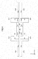
- FIG. 4 is a diagram for describing a configuration of slots according to the one embodiment.
- the first slot 201 and the second slot 202 are formed to have the same width W0.
- One end portion 401A of the first slot 201 is coupled with a first adjustment slot 403A that has a width W1 broader than the first slot 201, and extends in a direction orthogonal to the first slot 201 (the plus Y-axis direction).
- another end portion 401B of the first slot 201 is coupled with a second adjustment slot 403B that has the width W1 broader than the first slot 201, and extends in a direction orthogonal to the first slot 201 (the plus Y-axis direction).
- the end portion 401A, 401B, and the like are illustrated with dashed lines, these lines are imaginary line for showing the boundaries of the slots and do not actually exist. The same applies to the other dashed lines in FIG. 4 .
- one end portion 402A of the second slot 202 is coupled with a third adjustment slot 403C that has the width W1 broader than the second slot 202, and extends in a direction orthogonal to the second slot 202 (the minus Y-axis direction).
- another end portion 402B of the second slot 202 is coupled with a fourth adjustment slot 403D that has the width W1 broader than the second slot 202, and extends in a direction orthogonal to the second slot 202 (the minus Y-axis direction).
- any adjustment slot is indicated from among the first adjustment slot 403A, the second adjustment slot 403B, the third adjustment slot 403C, and the fourth adjustment slot 403D, it will be referred to as an "adjustment slot 403".
- the width W1 is formed to be the same for the respective adjustment slots 403. However, it is not limited as such, and the width of the adjustment slots 403 may vary from one adjustment slot 403 to another. Note that the adjustment slots 403 can be used for, for example, adjustment of the impedance matching between the antenna 200 and the IC chip 104, adjustment of the resonance frequency of the antenna 200, and the like.
- the antenna 200 further includes a first expansion slot 404A, a second expansion slot 404B, a third expansion slot 404C, and a fourth expansion slot 404D.
- the first expansion slot 404A is formed to be coupled with the first slot 201 via the first adjustment slot 403A, to be parallel to the first slot 201, and to extend in a direction away from the first slot 201 (the minus X-axis direction).
- the first expansion slot 404A is coupled with the first adjustment slot 403A at a position opposite to the position at which the first slot 201 is coupled.
- the second expansion slot 404B is formed to be coupled with the first slot 201 via the second adjustment slot 403B, to be parallel to the first slot 201, and to extend in a direction away from the first slot 201 (the plus X-axis direction).
- the second expansion slot 404B is coupled with the second adjustment slot 403B at a position opposite to the position at which the first slot 201 is coupled.
- the third expansion slot 404C is formed to be coupled with the second slot 202 via the third adjustment slot 403C, to be parallel to the second slot 202, and to extend in a direction away from the second slot 202 (the minus X-axis direction).
- the third expansion slot 404C is coupled with the third adjustment slot 403C at a position opposite to the position at which the second slot 202 is coupled.
- the fourth expansion slot 404D is formed to be coupled with the second slot 202 via the fourth adjustment slot 403D, to be parallel to the second slot 202, and to extend in a direction away from the second slot 202 (the plus X-axis direction).
- the fourth expansion slot 404D is coupled with the fourth adjustment slot 403D at a position opposite to the position at which the second slot 202 is coupled. Note that in the following description, in the case where any expansion slot is indicated from among the first expansion slot 404A, the second expansion slot 404B, the third expansion slot 404C, and the fourth expansion slot 404D, it will be referred to as an "expansion slot 404".
- the width W2 is formed to be the same for the respective expansion slots 404. However, it is not limited as such, and the width of the expansion slots 404 may vary, for example, from one expansion slot 404 to another. Note that the expansion slot 404 is used for, for example, adjustment of the impedance matching between the antenna 200 and the IC chip 104, adjustment of the resonance frequency of the antenna 200, and the like.
- W0 can be set to 1.00 mm to 3.00 mm, favorably 1.50 mm to 2.5 mm.
- W1 can be set to 4.00 mm to 10.00 mm, favorably 5.00 mm to 8.00 mm.
- W2 can be set to 0.8 mm to 2.00 mm, favorably 1.0 mm to 1.5 mm.
- W3 can be set to 0.5 mm to 1.5 mm, favorably 0.7 mm to 1.3 mm.
- FIG. 5 includes diagrams illustrating one example of a specific configuration of the RFID tag according to the one embodiment. This figure illustrates an example of a specific configuration of the RFID tag 100 produced by the inventors, with which good results were obtained.
- FIG. 5(A) illustrates the layer configuration of the produced RFID tag 100.
- the RFID tag 100 is provided with a first conductive layer 101 serving as the ground plane, a second conductive layer 102 in which an antenna 200 is formed, and an insulating layer 103 provided between the first conductive layer 101 and the second conductive layer 102. Also, the first conductive layer 101 is affixed to an object to be affixed 500 via the first resin layer 105.
- the conductor For the first conductive layer 101 and the second conductive layer 102, aluminum (a thickness of 10 ⁇ m) was used as the conductor. However, as the conductor, for example, metal other than aluminum such as copper may be used.
- acrylic foam (a thickness of 300 ⁇ m) was used as the insulator.
- an insulator other than acrylic form such as urethane foam may be used as the insulator.
- FIG. 5(B) illustrates the shape of the antenna 200 formed in the second conductive layer 102 of the produced RFID tag 100.
- L0 can be set to 9.00 mm to 13.00 mm, favorably 10.00 mm to 12.00 mm.
- L1 can be set to 2.50 mm to 5.00 mm, favorably 3.00 mm to 4.00 mm.
- L2 can be set to 10.00 mm to 15.00 mm, favorably 11.50 mm to 13.50 mm.
- the central portion 203 as illustrated in FIG. 3 was formed at the center of the second conductive layer 102, and the IC chip 104 was electrically connected between the attachment patterns 302A and 302B.
- the first slot 201 and the second slot were formed to extend in a direction parallel to the long side (one side) of the rectangle (the X-axis direction).
- the width W0 of the first slot 201 and the second slot 202 was set to 1.90 mm
- the width W3 of the first conductive portion 301A and the second conductive portion 301B was set to 1.00 mm.
- the length L0 of the first slot 201 and the second slot was set to 10.80 mm.
- the first to fourth adjustment slots 403 and the first to fourth expansion slots 404 were formed so as to be line symmetric with respect to a centerline 501 of the second conductive layer 102 in the Y-axis direction, and to be line symmetric with respect to a centerline 502 in the X-axis direction.
- the width W1 of the adjustment slot 403 was set to 6.50 mm and the length L1 was set to 3.6 mm.
- the width W2 of the expansion slot 404 was set to 1.30 mm and the length L2 was set to 12.50 mm. Note that the dimensions of the respective portions were determined by producing prototypes to determine the best balance between the center frequency and the communication distance.
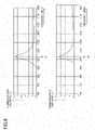
- FIG. 6 includes diagrams illustrating an example of communication characteristics of the antenna according to the one embodiment.
- FIG. 6(A) illustrates an example of a measurement result obtained by measuring the relationship between the frequency and the communication distance with a commercially available RFID tag/label performance inspection device, in the case where a metal plate (a stainless steel plate) was used as the object to be affixed 500 for the RFID tag 100 described in FIG. 5 .
- a metal plate a stainless steel plate
- the horizontal axis indicates the frequency (MHz), and the vertical axis indicates the communication distance (m). Note that in the following description, a frequency at which a maximum communication distance of the RFID tag 100 is obtained will be referred to as a center frequency fc.
- the produced RFID tag 100 had a center frequency fc around 920 MHz that is commonly used in an RFID system, and a communication distance of 3 m or longer at the center frequency fc. As such, the produced RFID tag 100 was confirmed to have good communication characteristics when affixed to the metal plate.
- the center frequency fc of the RFID tag 100 can be adjusted to a predetermined frequency, for example, by changing the length L2 of the expansion slots 404. For example, by making the length L2 of the expansion slots 404 longer, the center frequency fc can be changed to a lower frequency. Also, by making the length L2 of the expansion slots 404 shorter, the center frequency fc can be changed to a higher frequency.
- FIG. 6(B) illustrates an example of a measurement result obtained by measuring the relationship between the frequency and the communication distance with an RFID tag/label performance inspection device, in the case where the object to be affixed 500 was paper in FIG. 5(A) .
- the produced RFID tag 100 exhibited little change in the center frequency fc even in the case of the object to be affixed 500 being paper, and at a frequency around 920 MHz commonly used in an RFID system, it was confirmed that the communication distance around 2 m could be secured.
- the RFID tag 100 the antenna 200 formed in the second conductive layer 102 is affixed to the object to be affixed 500 via the first conductive layer 101 serving as the ground plane, and hence, has a feature of being unlikely to be affected by the material of the object to be affixed 500.
- a metal-compatible RFID tag (the RFID tag 100) that includes the antenna 200 having a planar structure and is easy to manufacture and handle can be provided.
- the antenna 200 of the RFID tag 100 has a planar structure as described with FIGs. 1 to 5 . Therefore, for example, by pressing, etching, or plating of metal foil; silk screen printing of metal paste; or the likes, it can be manufactured more easily than conventional metal-compatible RFID tags having three-dimensional structures.
- the RFID tag 100 having a layer configuration as illustrated in FIG. 5(A) can be manufactured to have a thickness of approximately 500 to 600 ⁇ m, and hence, printing by a label printer, encoding, and the like can be performed.
- the antenna portion has a structure of protruding out of a metal object to be affixed; therefore, there is a risk that the RFID tag may fall off or be broken.
- the RFID tag 100 according to the present embodiment has a flat structure; therefore, the risk of falling off or breaking of the RFID tag 100 is reduced, and handling becomes easier.
- the RFID tag 100 and the antenna 200 illustrated in FIG. 5 can be modified and applied in a variety of ways.
- first to fourth modified examples having the layer configuration illustrated in FIG. 5(A) in which part of the configuration of the antenna 200 illustrated in FIG. 5(B) is modified, will be described.
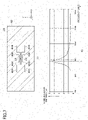
- FIG. 7 includes diagrams illustrating an example configuration of an antenna according to a first modified example and an example of communication characteristics.
- FIG. 7(A) illustrates an example configuration of the antenna 200 formed in the second conductive layer 102 of the RFID tag 100 according to the first modified example.
- the positions of the expansion slots 404 are changed, compared to the configuration of the antenna 200 according to the one embodiment described in FIG. 5(B) .
- the first expansion slot 404A has a coupling position with the first adjustment slot 403A shifted in the plus Y direction
- the second expansion slot 404B has a coupling position with the second adjustment slot 403B shifted in the plus Y direction.
- the third expansion slot 404C has a coupling position with the third adjustment slot 403C shifted in the minus Y direction
- the fourth expansion slot 404D has a coupling position with the fourth adjustment slot 403D shifted in the plus Y direction.
- FIG. 7(B) illustrates an example of a measurement result showing the relationship between the frequency and the communication distance, in the case where the object to be affixed 500 is a metal plate in the RFID tag 100 in which the antenna 200 according to the first modified example as illustrated in FIG. 7(A) is formed in the second conductive layer 102.
- FIG. 8 is a diagram illustrating an example configuration of an antenna according to a second modified example. This figure illustrates an example configuration of the antenna 200 formed in the second conductive layer 102 of the RFID tag 100 according to the second modified example.
- the antenna 200 according to the second modified example has a configuration in which the expansion slots 404 included in the configuration of the antenna 200 according to the one embodiment described in FIG. 5(B) are omitted.
- the center frequency fc can be changed by changing the length L1 of the adjustment slots 403, instead of the length L2 of the expansion slots 404.
- FIG. 9(A) illustrates an example of a measurement result showing the relationship between the frequency and the communication distance in the case where an RFID tag 100 having a length L1 of the adjustment slots 403 being 3.6 mm is affixed to a metal plate, in the antenna 200 according to the second modified example as illustrated in FIG. 8 .
- the center frequency fc increases from around 920 MHz to around 1090 MHz. Accordingly, it can be stated that the expansion slot 404 has an effect of lowering the center frequency fc in the antenna 200 according to the second modified example as illustrated in FIG. 8 .
- FIG. 9(B) illustrates an example of a measurement result showing the relationship between the frequency and the communication distance in the case where an RFID tag 100 having a length L1 of the adjustment slots 403 being 4.6 mm is affixed to a metal plate, in the antenna 200 according to the second modified example as illustrated in FIG. 8 .
- the center frequency fc decreases from around 1900 MHz to around 1020 MHz. Accordingly, by making the length L1 of the expansion slot 404 longer, it can be considered that the center frequency fc can be adjusted to a lower frequency.
- FIG. 9(C) illustrates an example of a measurement result showing the relationship between the frequency and the communication distance in the case where an RFID tag 100 having a length L1 of the adjustment slots 403 being 5.1 mm is affixed to a metal plate, in the antenna 200 according to the second modified example as illustrated in FIG. 8 .
- the communication distance around 940 MHz is around 2.5 m, and in the case where the length L1 of the adjustment slots 403 is formed to be a bit longer to set the center frequency fc to 920 MHz, there is a likelihood that the communication distance becomes further shorter.
- the antenna 200 according to the second modified example as illustrated in FIG. 8 can be adopted.
- the center frequency fc can be changed by changing the width W1 of the adjustment slots 403.
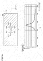
- FIG. 10 includes diagrams illustrating an example configuration of an antenna according to a third modified example.
- FIG. 10(A) illustrates an example configuration of the antenna 200 formed in the second conductive layer 102 of the RFID tag 100 according to the third modified example.
- the antenna 200 according to the third modified example has a configuration in which the third expansion slot 404C and the fourth expansion slot 404D from among the expansion slots 404 included in the configuration of the antenna 200 according to the one embodiment described in FIG. 5(B) are omitted.
- the antenna 200 according to the third modified example may have a configuration in which the first expansion slot 404A and the second expansion slot 404B are omitted, whereas the third expansion slot 404C and the fourth expansion slot 404D are provided. In this way, the antenna 200 may have some of the expansion slots 404 omitted.
- FIG. 10(B) illustrates an example of a measurement result showing the relationship between the frequency and the communication distance, in the case where the object to be affixed 500 is a metal plate in the RFID tag 100 in which the antenna 200 according to the third modified example as illustrated in FIG. 10(A) is formed in the second conductive layer 102.
- the center frequency fc increases from around 920 MHz to around 970 MHz.
- the center frequency fc can be adjusted around 920 MHz commonly used in an RFID system.
- the antenna 200 according to the third modified example has an asymmetric configuration of the expansion slots 404; therefore, for example, there is a likelihood that in the XY plane, the directional characteristic of the antenna 200 is also asymmetric.
- the directional characteristic of the antenna 200 can be asymmetric or is desired to be asymmetric; in such cases, there is a likelihood that the antenna 200 according to the third modified example as illustrated in FIG. 10 can be adopted.
- FIG. 11 includes diagrams illustrating an example configuration of an antenna according to a fourth modified example.
- FIG. 11(A) illustrates an example configuration of the antenna 200 formed in the second conductive layer 102 of the RFID tag 100 according to the fourth modified example.
- the antenna 200 according to the fourth modified example has a configuration in which the length L2 of the first expansion slot 404A and the second expansion slot 404B in the antenna 200 according to the one embodiment described in FIG. 5(B) is extended to 15.00 mm.
- the antenna 200 according to the fourth modified example may have a configuration in which the length L2 of the third expansion slot 404C and the fourth expansion slot 404D is extended to 15.00 mm. In this way, in the antenna 200, the length L2 of the respective expansion slots 404 is not necessarily the same.
- FIG. 11(B) illustrates an example of a measurement result showing the relationship between the frequency and the communication distance, in the case where the object to be affixed 500 is a metal plate in the RFID tag 100 in which the antenna 200 according to the fourth modified example as illustrated in FIG. 11(A) is formed in the second conductive layer 102.
- the center frequency fc increases from around 920 MHz to around 990 MHz.
- the center frequency fc can be adjusted lower.
- the center frequency fc is shifted to a higher frequency. In this way, in the case where some of the lengths L2 of the expansion slots 404 are different, unexpected measurement results may be obtained. Therefore, for example, in the case where the length L2 of the four expansion slots 404 is changed uniformly, and a good result is not obtained, there is a likelihood that the situation can be overcome by changing the length L2 of some of the expansion slots 404 from among the four expansion slots 404.
Landscapes
- Engineering & Computer Science (AREA)
- Microelectronics & Electronic Packaging (AREA)
- Computer Networks & Wireless Communication (AREA)
- Computer Hardware Design (AREA)
- Physics & Mathematics (AREA)
- General Physics & Mathematics (AREA)
- Theoretical Computer Science (AREA)
- Details Of Aerials (AREA)
- Waveguide Aerials (AREA)
Abstract
Description
- The present invention relates to an RFID (Radio Frequency Identification) tag and an antenna.
- For logistic management and product management, RFID tags affixed to objects to be affixed have become popular. An RFID tag is provided with an IC chip and an antenna electrically connected to the IC chip. The RFID tag is also referred to as a radio tag, IC tag, RF-ID tag, RF tag, or the like.
- When a typical RFID tag is affixed to an object to be affixed, for example, made of metal or the like, in some cases, the communication distance may become shorter; in order to cope with such a problem, RFID tags corresponding to objects to be affixed made of metal (referred to as the metal-compatible RFID tag, hereafter) have been proposed (see, for example,
Patent Documents 1 to 3). -
- [Patent Document 1]
WO 2016/129542 - [Patent Document 2] Published
Japanese Translation of PCT International Application 2019-533860 - [Patent Document 3]
Japanese Laid-Open Patent Application 2016-170576 - A conventional metal-compatible RFID tag, for example, as described in
Patent Documents 1 to 3, includes an antenna having a three-dimensional structure; therefore, difficulties may arise when manufacturing and handling these RFID tags. - One embodiment of the present invention is devised in view of the problem above, to provide a metal-compatible RFID tag that includes an antenna having a planar structure and is easy to manufacture and handle.
- In order to solve the problem described above, an RFID tag according to one embodiment of the present invention includes a first conductive layer; a second conductive layer in which an antenna is formed; an insulating layer provided between the first conductive layer and the second conductive layer; and an IC chip connected to the antenna. The antenna includes a first slot; a second slot facing the first slot; a coupling slot configured to couple a central portion of the first slot with a central portion of the second slot; a first adjustment slot coupled with one end of the first slot, being wider than the first slot, and extending in a direction orthogonal to the first slot; a second adjustment slot coupled with another end of the first slot, being wider than the first slot, and extending in a direction orthogonal to the first slot; a third adjustment slot coupled with one end of the second slot, being wider than the second slot, and extending in a direction orthogonal to the second slot; and a fourth adjustment slot coupled with another end of the second slot, being wider than the second slot, and extending in a direction orthogonal to the second slot.
- According to one embodiment of the present invention, an RFID tag that includes an antenna having a planar structure and is easy to manufacture and handle can be provided.
-
-
FIG. 1 is a diagram illustrating an example of a layer configuration of an RFID tag according to one embodiment; -
FIG. 2 is a diagram illustrating an example of a shape of the antenna according to the one embodiment; -
FIG. 3 is a diagram illustrating one example of the shape of the central portion in the antenna according to the one embodiment; -
FIG. 4 is a diagram for describing a configuration of slots of the antenna according to the one embodiment; -
FIG. 5 includes diagrams illustrating one example of the RFID tag according to one embodiment according to the one embodiment; -
FIG. 6 includes diagrams illustrating an example of communication characteristics of the antenna according to the one embodiment; -
FIG. 7 includes diagrams illustrating an example configuration of an antenna according to a first modified example and an example of communication characteristics; -
FIG. 8 is a diagram illustrating an example configuration of an antenna according to a second modified example; -
FIG. 9 includes diagrams illustrating an example of communication characteristics of an RFID tag according to the second modified example; -
FIG. 10 includes diagrams illustrating an example configuration of an antenna according to a third modified example and an example of communication characteristics; and -
FIG. 11 includes diagrams illustrating an example configuration of an antenna according to a fourth modified example and an example of communication characteristics. - In the following, with reference to the drawings, embodiments according to the present invention will be described in detail. In the following description, for common parts throughout the drawings, the same reference numerals may be assigned, and the description may be omitted. Also, for ease of understanding, the scale of parts in the drawings may differ from a scale of actual cases. A direction as described being parallel, perpendicular, orthogonal, horizontal, vertical, longitudinal, lateral, and so forth, is assumed to have deviation an extent not impairing effects of embodiments. Also, the X-axis direction, the Y-axis direction, and the Z-axis direction include a direction parallel to the X-axis, a direction parallel to the Y-axis, and a direction parallel to the Z-axis, respectively. The X-axis direction, the Y-axis direction, and the Z-axis direction are orthogonal to each other. The XY-plane, the YZ-plane, and the ZX-plane include a virtual plane parallel to the X-axis direction and the Y-axis direction, a virtual plane parallel to the Y-axis direction and the Z-axis direction, and a virtual plane parallel to the Z-axis direction and the X-axis direction, respectively. In
FIG. 1 and thereafter, in the X-axis direction, a direction indicated by an arrow is defined as the plus X-axis direction and a direction opposite to the direction is defined as the minus X-axis direction. In the Y-axis direction, a direction indicated by an arrow is defined as the plus Y-axis direction and a direction opposite to the direction is defined as the minus Y-axis direction. In the Z-axis direction, a direction indicated by an arrow is defined as the plus Z-axis direction and a direction opposite to the direction is defined as the minus Z-axis direction. -
FIG. 1 is a diagram illustrating an example of a layer configuration of an RFID tag according to one embodiment. An RFID (Radio Frequency Identification)tag 100 includes, for example, a firstconductive layer 101 serving as the ground plane, a secondconductive layer 102 in which an antenna is formed, aninsulating layer 103 provided between the firstconductive layer 101 and the secondconductive layer 102, anIC chip 104 connected to the antenna, and the like. - The first
conductive layer 101 and the secondconductive layer 102 are formed of a conductor having high conductivity (e.g., metal such as copper, aluminum, or the like). Note that the firstconductive layer 101 and the secondconductive layer 102 may be formed of the same conductor, or may be formed of different conductors. Theinsulating layer 103 is formed of an insulator having low conductivity (e.g., synthetic resin, rubber, etc., favorably foamed plastic such as urethane foam, acrylic foam, etc.). Note that the thickness of theinsulating layer 103 can be defined discretionarily. For example, in the case where the operating frequency of theRFID tag 100 is 920 MHz, the thickness of theinsulating layer 103 may be set to 100 µm to 500 µm, favorably 200 µm to 400 µm. Also, the thickness of the firstconductive layer 101 and the secondconductive layer 102 is designed to be sufficiently thinner than the thickness of the thickness of theinsulating layer 103. For example, the thickness of each of the firstconductive layer 101 and the secondconductive layer 102 may be set to 5 µm to 40 µm, favorably 7 µm to 35 µm. - The
IC chip 104 is an integrated circuit for an RFID system, and is connected to the antenna formed in the secondconductive layer 102. TheIC chip 104 receives a radio wave transmitted from a tag reader of an RFID system at a predetermined radio frequency (e.g., 860 MHz to 960 MHz), with the antenna, and generates electric power by the received radio wave to start its operation. Also, by using the generated electric power, theIC chip 104 transmits a radio wave including identification information recorded in advance on theIC chip 104 to the tag reader. - Also, as illustrated in
FIG. 1 , theRFID tag 100 may include afirst resin layer 105 or the like formed of, for example, a synthetic resin or the like, to form or hold the firstconductive layer 101, and/or asecond resin layer 107 formed of, for example, a synthetic resin or the like to form or hold the secondconductive layer 102. - Favorably, a surface of the
first resin layer 105 opposite to the surface contacting firstconductive layer 101 is a bonding surface, and by peeling off arelease paper 106, theRFID tag 100 can be affixed to an object to be affixed. Also, favorably, theRFID tag 100 is provided with apaper cover 108 on which printing or writing can be performed. - The
IC chip 104 has an internal capacity and is capable of securing a sufficient communication distance (e.g., around 1 m to 7 m) to communicate with a tag reader, by matching the impedance by an inductance component of the antenna and the internal capacity of theIC chip 104. - Next, using
FIGs. 2 to 4 , a configuration of the antenna formed in the secondconductive layer 102 will be described. -
FIG. 2 is a diagram illustrating an example of a shape of the antenna formed in the secondconductive layer 102. This figure illustrates a state of the secondconductive layer 102 illustrated inFIG. 1 as viewed from the minus Z-axis direction. As a favorable example, theantenna 200 may be formed in the secondconductive layer 102 having an outward appearance of, for example, a rectangle having a width W (W = around 85 to 105 mm) and a depth D (D = around 35 to 45 mm). Favorably, the other layers of theRFID tag 100 described inFIG. 1 also have an outward appearance of a rectangle corresponding to the secondconductive layer 102. However, it is not limited as such, and the layers of theRFID tag 100 may have an outward appearance other than a rectangle. - The
antenna 200 includes afirst slot 201; asecond slot 202 facing thefirst slot 202; and a coupling slot coupling thefirst slot 201 and thesecond slot 202 at acentral portion 203 of theantenna 200, that are provided in the secondconductive layer 102. Note that thecentral portion 203 and the coupling slot will be described later by usingFIG. 3 . - Favorably, the
first slot 201 and thesecond slot 202 are formed to extend in a direction parallel to one side (e.g., the long side) of the rectangle (the X-axis direction). - Note that in the present embodiment, within the area of the second
conductive layer 102, a portion where the conductor is not formed will be referred to as a "slot". Note that the secondconductive layer 102 and slots are formed by pressing, etching, or plating of metal foil of copper, aluminum, or the like; silk screen printing of metal paste; or the like. Note that inFIGs. 1 and2 , although the secondconductive layer 102 is hatched, this hatching is to indicate that the corresponding portion of the second conductive layer is a metal, and does not mean illustrating a pattern. -
FIG. 3 is a diagram illustrating one example of the shape of the central portion in the antenna according to the one embodiment. This figure is an enlarged view of thecentral portion 203 of theantenna 200 illustrated inFIG. 2 . InFIG. 3 , a conductive portion formed by the conductor between thefirst slot 201 and thesecond slot 202 is divided by acoupling slot 303 into two conductive portions of a firstconductive portion 301A and a secondconductive portion 301B. In other words, thecoupling slot 303 couples the central portion of thefirst slot 201 with the central portion of thesecond slot 202. - Also, as a favorable example, the first
conductive portion 301A and the secondconductive portion 301B haveattachment patterns IC chip 104 electrically connected. Note that the shape of theattachment patterns FIG. 3 is determined in consideration of the mountability of theIC chip 104, and other shapes may be adopted. - Further, a positioning pattern for the
IC chip 104 may be formed at thecentral portion 203. The positioning pattern is not connected to the other conductor portion within the secondconductive layer 102, and is held by, for example, thesecond resin layer 107 or the like. Note that the positioning pattern is a constituent element for manufacturing and is not included as a constituent element of theantenna 200, and hence, the description is omitted hereafter. -
FIG. 4 is a diagram for describing a configuration of slots according to the one embodiment. InFIG. 4 , thefirst slot 201 and thesecond slot 202 are formed to have the same width W0. - One
end portion 401A of thefirst slot 201 is coupled with afirst adjustment slot 403A that has a width W1 broader than thefirst slot 201, and extends in a direction orthogonal to the first slot 201 (the plus Y-axis direction). Also, anotherend portion 401B of thefirst slot 201 is coupled with asecond adjustment slot 403B that has the width W1 broader than thefirst slot 201, and extends in a direction orthogonal to the first slot 201 (the plus Y-axis direction). Note that inFIG. 4 , although theend portion FIG. 4 . - Similarly, one
end portion 402A of thesecond slot 202 is coupled with athird adjustment slot 403C that has the width W1 broader than thesecond slot 202, and extends in a direction orthogonal to the second slot 202 (the minus Y-axis direction). Also, anotherend portion 402B of thesecond slot 202 is coupled with afourth adjustment slot 403D that has the width W1 broader than thesecond slot 202, and extends in a direction orthogonal to the second slot 202 (the minus Y-axis direction). Note that in the following description, in the case where any adjustment slot is indicated from among thefirst adjustment slot 403A, thesecond adjustment slot 403B, thethird adjustment slot 403C, and thefourth adjustment slot 403D, it will be referred to as an "adjustment slot 403". - In the example in
FIG. 4 , the width W1 is formed to be the same for therespective adjustment slots 403. However, it is not limited as such, and the width of theadjustment slots 403 may vary from oneadjustment slot 403 to another. Note that theadjustment slots 403 can be used for, for example, adjustment of the impedance matching between theantenna 200 and theIC chip 104, adjustment of the resonance frequency of theantenna 200, and the like. - Favorably, the
antenna 200 further includes afirst expansion slot 404A, asecond expansion slot 404B, athird expansion slot 404C, and afourth expansion slot 404D. - The
first expansion slot 404A is formed to be coupled with thefirst slot 201 via thefirst adjustment slot 403A, to be parallel to thefirst slot 201, and to extend in a direction away from the first slot 201 (the minus X-axis direction). In the example inFIG. 4 , thefirst expansion slot 404A is coupled with thefirst adjustment slot 403A at a position opposite to the position at which thefirst slot 201 is coupled. - The
second expansion slot 404B is formed to be coupled with thefirst slot 201 via thesecond adjustment slot 403B, to be parallel to thefirst slot 201, and to extend in a direction away from the first slot 201 (the plus X-axis direction). In the example inFIG. 4 , thesecond expansion slot 404B is coupled with thesecond adjustment slot 403B at a position opposite to the position at which thefirst slot 201 is coupled. - The
third expansion slot 404C is formed to be coupled with thesecond slot 202 via thethird adjustment slot 403C, to be parallel to thesecond slot 202, and to extend in a direction away from the second slot 202 (the minus X-axis direction). In the example inFIG. 4 , thethird expansion slot 404C is coupled with thethird adjustment slot 403C at a position opposite to the position at which thesecond slot 202 is coupled. - The
fourth expansion slot 404D is formed to be coupled with thesecond slot 202 via thefourth adjustment slot 403D, to be parallel to thesecond slot 202, and to extend in a direction away from the second slot 202 (the plus X-axis direction). In the example inFIG. 4 , thefourth expansion slot 404D is coupled with thefourth adjustment slot 403D at a position opposite to the position at which thesecond slot 202 is coupled. Note that in the following description, in the case where any expansion slot is indicated from among thefirst expansion slot 404A, thesecond expansion slot 404B, thethird expansion slot 404C, and thefourth expansion slot 404D, it will be referred to as an "expansion slot 404". - In the example in
FIG. 4 , the width W2 is formed to be the same for therespective expansion slots 404. However, it is not limited as such, and the width of theexpansion slots 404 may vary, for example, from oneexpansion slot 404 to another. Note that theexpansion slot 404 is used for, for example, adjustment of the impedance matching between theantenna 200 and theIC chip 104, adjustment of the resonance frequency of theantenna 200, and the like. - Note that the dimensions of W0, W1, W2, and W3 that will be described later, can be defined discretionarily. For example, in the case where the operating frequency of the
RFID tag 100 is 920 MHz, W0 can be set to 1.00 mm to 3.00 mm, favorably 1.50 mm to 2.5 mm. W1 can be set to 4.00 mm to 10.00 mm, favorably 5.00 mm to 8.00 mm. W2 can be set to 0.8 mm to 2.00 mm, favorably 1.0 mm to 1.5 mm. W3 can be set to 0.5 mm to 1.5 mm, favorably 0.7 mm to 1.3 mm. - Next, an example of a more specific configuration of the
RFID tag 100 according to the present embodiment will be described. -
FIG. 5 includes diagrams illustrating one example of a specific configuration of the RFID tag according to the one embodiment. This figure illustrates an example of a specific configuration of theRFID tag 100 produced by the inventors, with which good results were obtained. -
FIG. 5(A) illustrates the layer configuration of the producedRFID tag 100. TheRFID tag 100 is provided with a firstconductive layer 101 serving as the ground plane, a secondconductive layer 102 in which anantenna 200 is formed, and an insulatinglayer 103 provided between the firstconductive layer 101 and the secondconductive layer 102. Also, the firstconductive layer 101 is affixed to an object to be affixed 500 via thefirst resin layer 105. - For the first
conductive layer 101 and the secondconductive layer 102, aluminum (a thickness of 10 µm) was used as the conductor. However, as the conductor, for example, metal other than aluminum such as copper may be used. - For the insulating
layer 103, acrylic foam (a thickness of 300 µm) was used as the insulator. However, as the insulator, for example, an insulator other than acrylic form such as urethane foam may be used. -
FIG. 5(B) illustrates the shape of theantenna 200 formed in the secondconductive layer 102 of the producedRFID tag 100. Theantenna 200 was formed to have the secondconductive layer 102 being a rectangular conductor having a lateral width of W=95.00 mm and a depth of D=40.00 mm, in which the first slot, thesecond slot 202, thecoupling slot 303, theadjustment slot 403, theexpansion slot 404, and the like are formed as described withFIGs. 3 and4 . - Note that the length L0 of the
first slot 201 and thesecond slot 202, the length L1 of the adjustment slots, and the length L2 of theexpansion slots 404 can be defined discretionarily. For example, in the case where the operating frequency of theRFID tag 100 is 920 MHz, L0 can be set to 9.00 mm to 13.00 mm, favorably 10.00 mm to 12.00 mm. L1 can be set to 2.50 mm to 5.00 mm, favorably 3.00 mm to 4.00 mm. L2 can be set to 10.00 mm to 15.00 mm, favorably 11.50 mm to 13.50 mm. - Note that the
central portion 203 as illustrated inFIG. 3 was formed at the center of the secondconductive layer 102, and theIC chip 104 was electrically connected between theattachment patterns first slot 201 and the second slot were formed to extend in a direction parallel to the long side (one side) of the rectangle (the X-axis direction). Note that the width W0 of thefirst slot 201 and thesecond slot 202 was set to 1.90 mm, and the width W3 of the firstconductive portion 301A and the secondconductive portion 301B was set to 1.00 mm. Also, the length L0 of thefirst slot 201 and the second slot was set to 10.80 mm. - Also, as illustrated in
FIG. 5(B) , the first tofourth adjustment slots 403 and the first tofourth expansion slots 404 were formed so as to be line symmetric with respect to acenterline 501 of the secondconductive layer 102 in the Y-axis direction, and to be line symmetric with respect to acenterline 502 in the X-axis direction. Note that the width W1 of theadjustment slot 403 was set to 6.50 mm and the length L1 was set to 3.6 mm. Also, the width W2 of theexpansion slot 404 was set to 1.30 mm and the length L2 was set to 12.50 mm. Note that the dimensions of the respective portions were determined by producing prototypes to determine the best balance between the center frequency and the communication distance. -
FIG. 6 includes diagrams illustrating an example of communication characteristics of the antenna according to the one embodiment.FIG. 6(A) illustrates an example of a measurement result obtained by measuring the relationship between the frequency and the communication distance with a commercially available RFID tag/label performance inspection device, in the case where a metal plate (a stainless steel plate) was used as the object to be affixed 500 for theRFID tag 100 described inFIG. 5 . - In
FIG. 6(A) , the horizontal axis indicates the frequency (MHz), and the vertical axis indicates the communication distance (m). Note that in the following description, a frequency at which a maximum communication distance of theRFID tag 100 is obtained will be referred to as a center frequency fc. - As illustrated in
FIG. 6(A) , the producedRFID tag 100 had a center frequency fc around 920 MHz that is commonly used in an RFID system, and a communication distance of 3 m or longer at the center frequency fc. As such, the producedRFID tag 100 was confirmed to have good communication characteristics when affixed to the metal plate. - Note that the center frequency fc of the
RFID tag 100 can be adjusted to a predetermined frequency, for example, by changing the length L2 of theexpansion slots 404. For example, by making the length L2 of theexpansion slots 404 longer, the center frequency fc can be changed to a lower frequency. Also, by making the length L2 of theexpansion slots 404 shorter, the center frequency fc can be changed to a higher frequency. -
FIG. 6(B) illustrates an example of a measurement result obtained by measuring the relationship between the frequency and the communication distance with an RFID tag/label performance inspection device, in the case where the object to be affixed 500 was paper inFIG. 5(A) . The producedRFID tag 100 exhibited little change in the center frequency fc even in the case of the object to be affixed 500 being paper, and at a frequency around 920 MHz commonly used in an RFID system, it was confirmed that the communication distance around 2 m could be secured. - In this way, the
RFID tag 100 according to the present embodiment, theantenna 200 formed in the secondconductive layer 102 is affixed to the object to be affixed 500 via the firstconductive layer 101 serving as the ground plane, and hence, has a feature of being unlikely to be affected by the material of the object to be affixed 500. - As described above, according to the one embodiment of the present invention, a metal-compatible RFID tag (the RFID tag 100) that includes the
antenna 200 having a planar structure and is easy to manufacture and handle can be provided. - For example, the
antenna 200 of theRFID tag 100 according to the present embodiment has a planar structure as described withFIGs. 1 to 5 . Therefore, for example, by pressing, etching, or plating of metal foil; silk screen printing of metal paste; or the likes, it can be manufactured more easily than conventional metal-compatible RFID tags having three-dimensional structures. - Also, for example, the
RFID tag 100 having a layer configuration as illustrated inFIG. 5(A) can be manufactured to have a thickness of approximately 500 to 600 µm, and hence, printing by a label printer, encoding, and the like can be performed. - Further, for example, in a metal-compatible RFIF tag as shown in
Patent Document 3, the antenna portion has a structure of protruding out of a metal object to be affixed; therefore, there is a risk that the RFID tag may fall off or be broken. In contrast, theRFID tag 100 according to the present embodiment has a flat structure; therefore, the risk of falling off or breaking of theRFID tag 100 is reduced, and handling becomes easier. - The
RFID tag 100 and theantenna 200 illustrated inFIG. 5 can be modified and applied in a variety of ways. Here, first to fourth modified examples having the layer configuration illustrated inFIG. 5(A) , in which part of the configuration of theantenna 200 illustrated inFIG. 5(B) is modified, will be described. -
FIG. 7 includes diagrams illustrating an example configuration of an antenna according to a first modified example and an example of communication characteristics.FIG. 7(A) illustrates an example configuration of theantenna 200 formed in the secondconductive layer 102 of theRFID tag 100 according to the first modified example. - As illustrated in
FIG. 7(A) , in theantenna 200 according to the first modified example, the positions of theexpansion slots 404 are changed, compared to the configuration of theantenna 200 according to the one embodiment described inFIG. 5(B) . For example, inFIG. 7(A) , thefirst expansion slot 404A has a coupling position with thefirst adjustment slot 403A shifted in the plus Y direction, and thesecond expansion slot 404B has a coupling position with thesecond adjustment slot 403B shifted in the plus Y direction. Also, thethird expansion slot 404C has a coupling position with thethird adjustment slot 403C shifted in the minus Y direction, and thefourth expansion slot 404D has a coupling position with thefourth adjustment slot 403D shifted in the plus Y direction. -
FIG. 7(B) illustrates an example of a measurement result showing the relationship between the frequency and the communication distance, in the case where the object to be affixed 500 is a metal plate in theRFID tag 100 in which theantenna 200 according to the first modified example as illustrated inFIG. 7(A) is formed in the secondconductive layer 102. - In the example in
FIG. 7(B) , compared to the measurement result of theRFID tag 100 according to the one embodiment illustrated inFIG. 6(A) , it can be seen that the center frequency fc decreases from around 920 MHz to around 880 MHz. - From this result, for example, as illustrated in
FIG. 7(A) , by shifting the coupling positions of theexpansion slot 404 and theadjustment slot 403 in the Y-axis direction, it can be inferred that the center frequency fc can be adjusted to a certain extent. - Also, for example, in the case where it is desirable to adjust the center frequency fc in a lower direction while not increasing the length of the
antenna 200 in the X-axis direction, one may consider adopting theantenna 200 according to the first modified example as illustrated inFIG. 7(A) . - Note that by shortening the length L2 of the
expansion slots 404 and adjusting the center frequency fc to come around 920 MHz, it can be considered that good characteristics are obtained for theantenna 200 according to the first modified example as an antenna for theRFID tag 100. -
FIG. 8 is a diagram illustrating an example configuration of an antenna according to a second modified example. This figure illustrates an example configuration of theantenna 200 formed in the secondconductive layer 102 of theRFID tag 100 according to the second modified example. - As illustrated in
FIG. 8 , theantenna 200 according to the second modified example has a configuration in which theexpansion slots 404 included in the configuration of theantenna 200 according to the one embodiment described inFIG. 5(B) are omitted. In theantenna 200 according to the second modified example as such, the center frequency fc can be changed by changing the length L1 of theadjustment slots 403, instead of the length L2 of theexpansion slots 404. -
FIG. 9(A) illustrates an example of a measurement result showing the relationship between the frequency and the communication distance in the case where anRFID tag 100 having a length L1 of theadjustment slots 403 being 3.6 mm is affixed to a metal plate, in theantenna 200 according to the second modified example as illustrated inFIG. 8 . - In the example in
FIG. 9(A) , compared to the measurement result of theRFID tag 100 according to the one embodiment illustrated inFIG. 6(A) , the center frequency fc increases from around 920 MHz to around 1090 MHz. Accordingly, it can be stated that theexpansion slot 404 has an effect of lowering the center frequency fc in theantenna 200 according to the second modified example as illustrated inFIG. 8 . -
FIG. 9(B) illustrates an example of a measurement result showing the relationship between the frequency and the communication distance in the case where anRFID tag 100 having a length L1 of theadjustment slots 403 being 4.6 mm is affixed to a metal plate, in theantenna 200 according to the second modified example as illustrated inFIG. 8 . - In the example in
FIG. 9(B) , compared to the measurement result illustrated inFIG. 9(A) , it can be seen that the center frequency fc decreases from around 1900 MHz to around 1020 MHz. Accordingly, by making the length L1 of theexpansion slot 404 longer, it can be considered that the center frequency fc can be adjusted to a lower frequency. -
FIG. 9(C) illustrates an example of a measurement result showing the relationship between the frequency and the communication distance in the case where anRFID tag 100 having a length L1 of theadjustment slots 403 being 5.1 mm is affixed to a metal plate, in theantenna 200 according to the second modified example as illustrated inFIG. 8 . - In the example in
FIG. 9(C) , compared to the measurement result illustrated inFIG. 9(B) , it can be seen that the center frequency fc decreases from around 1020 MHz to around 940 MHz. Therefore, by forming the length L1 of theadjustment slots 403 to be a bit longer, there is a likelihood that the center frequency fc can be adjusted around 920 MHz commonly used in an RFID system. - In contrast, as for the communication distance, in the example in
FIG. 9(C) , the communication distance around 940 MHz is around 2.5 m, and in the case where the length L1 of theadjustment slots 403 is formed to be a bit longer to set the center frequency fc to 920 MHz, there is a likelihood that the communication distance becomes further shorter. However, for example, for applications in which the communication distance around 2 m is sufficient, theantenna 200 according to the second modified example as illustrated inFIG. 8 can be adopted. - Note that in the
antenna 200 according to the second modified example as illustrated inFIG. 8 , although only the length L1 of theadjustment slots 403 is changed, the center frequency fc can be changed by changing the width W1 of theadjustment slots 403. -
FIG. 10 includes diagrams illustrating an example configuration of an antenna according to a third modified example.FIG. 10(A) illustrates an example configuration of theantenna 200 formed in the secondconductive layer 102 of theRFID tag 100 according to the third modified example. - As illustrated in
FIG. 10(A) , theantenna 200 according to the third modified example has a configuration in which thethird expansion slot 404C and thefourth expansion slot 404D from among theexpansion slots 404 included in the configuration of theantenna 200 according to the one embodiment described inFIG. 5(B) are omitted. Note that theantenna 200 according to the third modified example may have a configuration in which thefirst expansion slot 404A and thesecond expansion slot 404B are omitted, whereas thethird expansion slot 404C and thefourth expansion slot 404D are provided. In this way, theantenna 200 may have some of theexpansion slots 404 omitted. -
FIG. 10(B) illustrates an example of a measurement result showing the relationship between the frequency and the communication distance, in the case where the object to be affixed 500 is a metal plate in theRFID tag 100 in which theantenna 200 according to the third modified example as illustrated inFIG. 10(A) is formed in the secondconductive layer 102. - In the example in
FIG. 10(B) , compared to the measurement result of theRFID tag 100 according to the one embodiment illustrated inFIG. 6(A) , the center frequency fc increases from around 920 MHz to around 970 MHz. In this case, for example, by making the length L2 of thefirst expansion slot 404A and thesecond expansion slot 404B further longer, there is a likelihood that the center frequency fc can be adjusted around 920 MHz commonly used in an RFID system. - However, as illustrated in
FIG. 10 , theantenna 200 according to the third modified example has an asymmetric configuration of theexpansion slots 404; therefore, for example, there is a likelihood that in the XY plane, the directional characteristic of theantenna 200 is also asymmetric. However, depending on the application, there are cases where the directional characteristic of theantenna 200 can be asymmetric or is desired to be asymmetric; in such cases, there is a likelihood that theantenna 200 according to the third modified example as illustrated inFIG. 10 can be adopted. -
FIG. 11 includes diagrams illustrating an example configuration of an antenna according to a fourth modified example.FIG. 11(A) illustrates an example configuration of theantenna 200 formed in the secondconductive layer 102 of theRFID tag 100 according to the fourth modified example. - As illustrated in
FIG. 11(A) , theantenna 200 according to the fourth modified example has a configuration in which the length L2 of thefirst expansion slot 404A and thesecond expansion slot 404B in theantenna 200 according to the one embodiment described inFIG. 5(B) is extended to 15.00 mm. Note that theantenna 200 according to the fourth modified example may have a configuration in which the length L2 of thethird expansion slot 404C and thefourth expansion slot 404D is extended to 15.00 mm. In this way, in theantenna 200, the length L2 of therespective expansion slots 404 is not necessarily the same. -
FIG. 11(B) illustrates an example of a measurement result showing the relationship between the frequency and the communication distance, in the case where the object to be affixed 500 is a metal plate in theRFID tag 100 in which theantenna 200 according to the fourth modified example as illustrated inFIG. 11(A) is formed in the secondconductive layer 102. - In the example in
FIG. 11(B) , compared to the measurement result of theRFID tag 100 according to the one embodiment illustrated inFIG. 6(A) , the center frequency fc increases from around 920 MHz to around 990 MHz. - In the description of the
antenna 200 according to the one embodiment illustrated inFIG. 5(B) , it has been described that by making the length L2 of theexpansion slot 404 longer, the center frequency fc can be adjusted lower. However, in theantenna 200 according to the fourth modified example, the center frequency fc is shifted to a higher frequency. In this way, in the case where some of the lengths L2 of theexpansion slots 404 are different, unexpected measurement results may be obtained. Therefore, for example, in the case where the length L2 of the fourexpansion slots 404 is changed uniformly, and a good result is not obtained, there is a likelihood that the situation can be overcome by changing the length L2 of some of theexpansion slots 404 from among the fourexpansion slots 404. - The configuration illustrated in each of the embodiment and examples described above shows one example of the contents of the present invention, which may be combined with other publicly known techniques, and part of the configuration can also be omitted or changed, without deviating from the gist of the present invention.
- The present application claims priority to a base application No.
2020-026431, filed on February 19, 2020, with the Japan Patent Office -
- 100
- RFID tag
- 101
- first conductive layer
- 102
- second conductive layer
- 103
- insulation layer
- 104
- IC chip
- 201
- first slot
- 202
- second slot
- 301A
- first conductive portion
- 301B
- second conductive portion
- 303
- coupling slot
- 403A
- first adjustment slot
- 403B
- second adjustment slot
- 403C
- third adjustment slot
- 403D
- fourth adjustment slot
- 404A
- first expansion slot
- 404B
- second expansion slot
- 404C
- third expansion slot
- 404D
- fourth expansion slot
Claims (10)
- An RFID tag comprising:a first conductive layer;a second conductive layer in which an antenna is formed;an insulating layer provided between the first conductive layer and the second conductive layer; andan IC chip connected to the antenna,wherein the antenna includesa first slot,a second slot facing the first slot,a coupling slot configured to couple a central portion of the first slot with a central portion of the second slot,a first adjustment slot coupled with one end of the first slot, being wider than the first slot, and extending in a direction orthogonal to the first slot,a second adjustment slot coupled with another end of the first slot, being wider than the first slot, and extending in a direction orthogonal to the first slot,a third adjustment slot coupled with one end of the second slot, being wider than the second slot, and extending in a direction orthogonal to the second slot, anda fourth adjustment slot coupled with another end of the second slot, being wider than the second slot, and extending in a direction orthogonal to the second slot.
- The RFID tag as claimed in claim 1, further comprising:a first expansion slot coupled with the first slot through the first adjustment slot, and being parallel to the first slot, and extending in a direction away from the first slot; anda second expansion slot coupled with the first slot through the second adjustment slot, and being parallel to the first slot, and extending in a direction away from the first slot.
- The RFID tag as claimed in claim 2, further comprising:a third expansion slot coupled with the second slot through the third adjustment slot, being parallel to the second slot, and extending in a direction away from the second slot; anda fourth expansion slot coupled with the second slot through the fourth adjustment slot, being parallel to the second slot, and extending in a direction away from the second slot.
- The RFID tag as claimed in any one of claims 1 to 3, wherein the coupling slot divides a conductive portion formed between the first slot and the second slot into two portions, and
wherein the IC chip is electrically connected between the two divided conductive portions. - The RFID tag as claimed in any one of claims 1 to 3, wherein an outward appearance of the second conductive layer is a rectangle, and
wherein the first slot and the second slot extend in a direction parallel to one side of the rectangle. - The RFID tag as claimed in any one of claims 1 to 5, wherein the first adjustment slot and the second adjustment slot extend in a direction away from the second slot, and
wherein the third adjustment slot and the fourth adjustment slot extend in a direction away from the first slot. - The RFID tag as claimed in any one of claims 1 to 6, wherein impedance matching between the IC chip and the antenna, or a resonance frequency of the antenna is adjusted according to a shape of the first adjustment slot, the second adjustment slot, the third adjustment slot, and the fourth adjustment slot.
- The RFID tag as claimed in claim 3, wherein impedance matching between the IC chip and the antenna, or a resonance frequency of the antenna is adjusted according to a shape of the first expansion slot, the second expansion slot, the third expansion slot, and the fourth expansion slot.
- The RFID tag as claimed in any one of claims 1 to 6, wherein the antenna is affixed to an object to be affixed via the first conductive layer.
- An antenna used in the RFID tag as claimed in any one of claims 1 to 9.
Applications Claiming Priority (2)
| Application Number | Priority Date | Filing Date | Title |
|---|---|---|---|
| JP2020026431A JP7470526B2 (en) | 2020-02-19 | 2020-02-19 | RFID tag and antenna |
| PCT/JP2021/005554 WO2021166852A1 (en) | 2020-02-19 | 2021-02-15 | Rfid tag, and antenna |
Publications (2)
| Publication Number | Publication Date |
|---|---|
| EP4109338A1 true EP4109338A1 (en) | 2022-12-28 |
| EP4109338A4 EP4109338A4 (en) | 2023-07-26 |
Family
ID=77391187
Family Applications (1)
| Application Number | Title | Priority Date | Filing Date |
|---|---|---|---|
| EP21756995.3A Withdrawn EP4109338A4 (en) | 2020-02-19 | 2021-02-15 | Rfid tag, and antenna |
Country Status (6)
| Country | Link |
|---|---|
| US (1) | US20230106699A1 (en) |
| EP (1) | EP4109338A4 (en) |
| JP (1) | JP7470526B2 (en) |
| CN (1) | CN115023706A (en) |
| TW (1) | TW202139067A (en) |
| WO (1) | WO2021166852A1 (en) |
Families Citing this family (2)
| Publication number | Priority date | Publication date | Assignee | Title |
|---|---|---|---|---|
| WO2023084697A1 (en) * | 2021-11-11 | 2023-05-19 | 立山科学株式会社 | Rf tag |
| JP7568186B2 (en) * | 2022-08-26 | 2024-10-16 | 大王製紙株式会社 | RFID tags |
Family Cites Families (24)
| Publication number | Priority date | Publication date | Assignee | Title |
|---|---|---|---|---|
| KR100312364B1 (en) * | 1997-05-30 | 2001-12-28 | 가나이 쓰도무 | Tunable slot antenna |
| JPWO2007013168A1 (en) * | 2005-07-29 | 2009-02-05 | 富士通株式会社 | RF tag and method of manufacturing RF tag |
| WO2007102360A1 (en) * | 2006-03-06 | 2007-09-13 | Mitsubishi Electric Corporation | Rfid tag, method for manufacturing rfid tag and method for arranging rfid tag |
| FR2903216A1 (en) * | 2006-06-28 | 2008-01-04 | Thomson Licensing Sa | IMPROVING DATA MEDIA SUCH AS OPTICAL MEDIA |
| ATE468628T1 (en) * | 2007-07-24 | 2010-06-15 | Pepperl & Fuchs | SLOT ANTENNA AND METHOD FOR RFID |
| TWI423519B (en) * | 2007-09-04 | 2014-01-11 | Mitsubishi Electric Corp | Radio frequency identification tag |
| US8743006B2 (en) * | 2007-10-31 | 2014-06-03 | Nitta Corporation | Wireless communication-improving sheet member, wireless IC tag, antenna, and wireless communication system using the same |
| JP2010081290A (en) | 2008-09-26 | 2010-04-08 | Mitsubishi Electric Corp | RFID tag |
| JP5146265B2 (en) * | 2008-11-04 | 2013-02-20 | 富士通株式会社 | Tag antenna and wireless tag including the same |
| JP5113727B2 (en) * | 2008-11-20 | 2013-01-09 | 株式会社日立製作所 | Wireless IC tag |
| CN101777693A (en) * | 2010-03-12 | 2010-07-14 | 浙江大学 | Ultrahigh frequency radio frequency identification anti-metal tag antenna with plane structure |
| JP5687154B2 (en) | 2011-08-11 | 2015-03-18 | 株式会社リコー | RFID tag and RFID system |
| JP2014041443A (en) | 2012-08-22 | 2014-03-06 | Ricoh Co Ltd | Rfid tag and rfid system |
| JP2014041444A (en) * | 2012-08-22 | 2014-03-06 | Ricoh Co Ltd | Rfid tag and rfid system |
| FR3023638B1 (en) * | 2014-07-11 | 2016-07-29 | Systemes Et Tech Identification (Stid) | RADIO-IDENTIFICATION LABEL IN THE ULTRA-HIGH FREQUENCY RANGE FOR BINDING ENVIRONMENT |
| TWI661607B (en) | 2015-02-10 | 2019-06-01 | 日商鳳凰解決方案股份有限公司 | RF tag antenna, RF tag, conductor with RF tag, and RF tag with box |
| JP2016170576A (en) | 2015-03-12 | 2016-09-23 | 凸版印刷株式会社 | Rfid label |
| CN106356613A (en) * | 2015-07-17 | 2017-01-25 | 西安中兴新软件有限责任公司 | Tag antenna and production method thereof |
| CN106503778A (en) * | 2015-09-08 | 2017-03-15 | 凸版印刷株式会社 | Band IC tag paster and its installation method |
| JP6668197B2 (en) * | 2016-08-18 | 2020-03-18 | 株式会社東芝 | Wireless device |
| US9875439B2 (en) * | 2017-06-27 | 2018-01-23 | Rfid Integrated Marketing Co., Ltd. | License plate radio electronic identifier |
| US10644407B2 (en) * | 2018-01-14 | 2020-05-05 | Wistron Neweb Corp. | Communication device |
| JP2020026431A (en) | 2018-08-10 | 2020-02-20 | 日本ケミファ株式会社 | Orally disintegrating tablets |
| JP7508237B2 (en) * | 2020-02-26 | 2024-07-01 | 日本航空電子工業株式会社 | Multi-band Antennas |
-
2020
- 2020-02-19 JP JP2020026431A patent/JP7470526B2/en active Active
-
2021
- 2021-02-15 WO PCT/JP2021/005554 patent/WO2021166852A1/en not_active Ceased
- 2021-02-15 US US17/760,216 patent/US20230106699A1/en not_active Abandoned
- 2021-02-15 EP EP21756995.3A patent/EP4109338A4/en not_active Withdrawn
- 2021-02-15 CN CN202180012096.1A patent/CN115023706A/en active Pending
- 2021-02-17 TW TW110105226A patent/TW202139067A/en unknown
Also Published As
| Publication number | Publication date |
|---|---|
| WO2021166852A1 (en) | 2021-08-26 |
| EP4109338A4 (en) | 2023-07-26 |
| JP7470526B2 (en) | 2024-04-18 |
| TW202139067A (en) | 2021-10-16 |
| CN115023706A (en) | 2022-09-06 |
| JP2021131700A (en) | 2021-09-09 |
| US20230106699A1 (en) | 2023-04-06 |
Similar Documents
| Publication | Publication Date | Title |
|---|---|---|
| CN101711430B (en) | Assembly of RF chips | |
| JP6485608B1 (en) | RFID tag | |
| US7126482B2 (en) | RFID tag and its manufacturing method | |
| JP5526726B2 (en) | Wireless tag | |
| KR100679502B1 (en) | RDF tag, antenna for RDF tag, antenna sheet for RDF tag, and RDF tag manufacturing method | |
| JP5703977B2 (en) | Metal articles with wireless communication devices | |
| US10396429B2 (en) | Wireless communication device | |
| US7924228B2 (en) | Storage medium with built-in antenna | |
| US11954552B2 (en) | RFID tag substrate, RFID tag, and RFID system | |
| JP2004062854A (en) | IC module, wireless information storage medium using the same, and wireless information transmitting / receiving device | |
| JP4478135B2 (en) | Antenna coil | |
| US11100382B2 (en) | Card-type wireless communication device | |
| JP2012253699A (en) | Wireless communication device, its manufacturing method, and metal article with wireless communication device | |
| TW201921799A (en) | RFID tag | |
| JP2012108843A (en) | RFID tag | |
| US10784562B2 (en) | Wireless communication chip having internal antenna, internal antenna for wireless communication chip, and method of fabricating wireless communication chip having internal antenna | |
| US20230106699A1 (en) | Rfid tag and antenna | |
| JP6590119B1 (en) | RFID tag and article with RFID | |
| US11962064B2 (en) | RFID tag and antenna | |
| JP2019004266A (en) | Antenna device and electronic apparatus | |
| CN113922069A (en) | Antenna device | |
| US20200042852A1 (en) | Rfid tag and method of manufacturing the same | |
| KR101102535B1 (en) | Isotropic Tag Antenna | |
| EP4124994B1 (en) | Rfid tag and antenna member for use in rfid tag | |
| JP2004173143A (en) | Connection part structure between antenna and communication cable |
Legal Events
| Date | Code | Title | Description |
|---|---|---|---|
| STAA | Information on the status of an ep patent application or granted ep patent |
Free format text: STATUS: THE INTERNATIONAL PUBLICATION HAS BEEN MADE |
|
| PUAI | Public reference made under article 153(3) epc to a published international application that has entered the european phase |
Free format text: ORIGINAL CODE: 0009012 |
|
| STAA | Information on the status of an ep patent application or granted ep patent |
Free format text: STATUS: REQUEST FOR EXAMINATION WAS MADE |
|
| 17P | Request for examination filed |
Effective date: 20220816 |
|
| AK | Designated contracting states |
Kind code of ref document: A1 Designated state(s): AL AT BE BG CH CY CZ DE DK EE ES FI FR GB GR HR HU IE IS IT LI LT LU LV MC MK MT NL NO PL PT RO RS SE SI SK SM TR |
|
| DAV | Request for validation of the european patent (deleted) | ||
| DAX | Request for extension of the european patent (deleted) | ||
| A4 | Supplementary search report drawn up and despatched |
Effective date: 20230627 |
|
| RIC1 | Information provided on ipc code assigned before grant |
Ipc: H01Q 1/38 20060101ALI20230621BHEP Ipc: H01Q 13/10 20060101ALI20230621BHEP Ipc: H01Q 9/16 20060101ALI20230621BHEP Ipc: H01Q 1/50 20060101ALI20230621BHEP Ipc: G06K 19/077 20060101AFI20230621BHEP |
|
| STAA | Information on the status of an ep patent application or granted ep patent |
Free format text: STATUS: THE APPLICATION IS DEEMED TO BE WITHDRAWN |
|
| 18D | Application deemed to be withdrawn |
Effective date: 20240125 |