EP4109286A1 - System on chip comprising a connection interface between master devices and slave devices - Google Patents
System on chip comprising a connection interface between master devices and slave devices Download PDFInfo
- Publication number
- EP4109286A1 EP4109286A1 EP22178614.8A EP22178614A EP4109286A1 EP 4109286 A1 EP4109286 A1 EP 4109286A1 EP 22178614 A EP22178614 A EP 22178614A EP 4109286 A1 EP4109286 A1 EP 4109286A1
- Authority
- EP
- European Patent Office
- Prior art keywords
- configuration parameters
- connection interface
- chip
- new configuration
- memory
- Prior art date
- Legal status (The legal status is an assumption and is not a legal conclusion. Google has not performed a legal analysis and makes no representation as to the accuracy of the status listed.)
- Pending
Links
Images


Classifications
-
- G—PHYSICS
- G06—COMPUTING OR CALCULATING; COUNTING
- G06F—ELECTRIC DIGITAL DATA PROCESSING
- G06F13/00—Interconnection of, or transfer of information or other signals between, memories, input/output devices or central processing units
- G06F13/14—Handling requests for interconnection or transfer
- G06F13/16—Handling requests for interconnection or transfer for access to memory bus
-
- G—PHYSICS
- G06—COMPUTING OR CALCULATING; COUNTING
- G06F—ELECTRIC DIGITAL DATA PROCESSING
- G06F15/00—Digital computers in general; Data processing equipment in general
- G06F15/76—Architectures of general purpose stored program computers
- G06F15/78—Architectures of general purpose stored program computers comprising a single central processing unit
- G06F15/7867—Architectures of general purpose stored program computers comprising a single central processing unit with reconfigurable architecture
- G06F15/7871—Reconfiguration support, e.g. configuration loading, configuration switching, or hardware OS
-
- G—PHYSICS
- G06—COMPUTING OR CALCULATING; COUNTING
- G06F—ELECTRIC DIGITAL DATA PROCESSING
- G06F15/00—Digital computers in general; Data processing equipment in general
- G06F15/16—Combinations of two or more digital computers each having at least an arithmetic unit, a program unit and a register, e.g. for a simultaneous processing of several programs
- G06F15/163—Interprocessor communication
- G06F15/173—Interprocessor communication using an interconnection network, e.g. matrix, shuffle, pyramid, star, snowflake
- G06F15/17356—Indirect interconnection networks
- G06F15/17368—Indirect interconnection networks non hierarchical topologies
- G06F15/17381—Two dimensional, e.g. mesh, torus
-
- G—PHYSICS
- G06—COMPUTING OR CALCULATING; COUNTING
- G06F—ELECTRIC DIGITAL DATA PROCESSING
- G06F13/00—Interconnection of, or transfer of information or other signals between, memories, input/output devices or central processing units
- G06F13/38—Information transfer, e.g. on bus
- G06F13/40—Bus structure
- G06F13/4063—Device-to-bus coupling
- G06F13/4068—Electrical coupling
-
- G—PHYSICS
- G06—COMPUTING OR CALCULATING; COUNTING
- G06F—ELECTRIC DIGITAL DATA PROCESSING
- G06F15/00—Digital computers in general; Data processing equipment in general
- G06F15/16—Combinations of two or more digital computers each having at least an arithmetic unit, a program unit and a register, e.g. for a simultaneous processing of several programs
- G06F15/163—Interprocessor communication
- G06F15/173—Interprocessor communication using an interconnection network, e.g. matrix, shuffle, pyramid, star, snowflake
- G06F15/17306—Intercommunication techniques
- G06F15/17312—Routing techniques specific to parallel machines, e.g. wormhole, store and forward, shortest path problem congestion
-
- G—PHYSICS
- G06—COMPUTING OR CALCULATING; COUNTING
- G06F—ELECTRIC DIGITAL DATA PROCESSING
- G06F15/00—Digital computers in general; Data processing equipment in general
- G06F15/76—Architectures of general purpose stored program computers
- G06F15/78—Architectures of general purpose stored program computers comprising a single central processing unit
- G06F15/7807—System on chip, i.e. computer system on a single chip; System in package, i.e. computer system on one or more chips in a single package
Definitions
- Embodiments of the present disclosure refers to a system on a chip (also known by the acronym "SoC"), and more particularly, to a connection interface between master devices and slave devices of the system on chip.
- SoC system on a chip
- a system on chip is an integrated electronic system configured to perform a plurality of functions.
- the system on chip can be used in an electronic device such as a microcontroller and can include a plurality of components.
- the components can comprise at least one processing core, one or more volatile and non-volatile memories, for example a flash memory, and a plurality of peripherals. Some of the components are used as master devices, such as the processing core. Other components are used as slave devices, such as the peripherals.
- connection interface can be a principal bus matrix or a connection interface inside a peripheral domain to address the different peripherals of the peripheral domain.
- connection interfaces are statically configured, for example in hard coded mode, so that, after a first initial configuration phase, the configuration of the bus matrix can no longer be changed.
- connection interfaces the versatility of the system on chip is limited.
- the communication between the components of the system on chip cannot be adapted to specific applications.
- a system on chip comprising:
- connection interface In such a system on chip, the operation of the connection interface can be modified with new configuration parameters.
- the system on chip presents an improved versality of use, thanks to the possibility of modifying the operation of the connection interface.
- such system on chip allows a route table and a remap table of the connection interface to be modified.
- the system on chip can also allow an arbiter policy of the connection interface to be modified so as to adapt the priorities between the master devices.
- the system on chip can also allow enabling or disabling the master devices and the slave devices.
- connection interface comprises:
- said at least one input stage, said at least one output stage and said at least one decoder are configured to operate according to said configuration parameters.
- the configuration bus is connected to said at least one input stage, to said at least one output stage and to said at least one decoder and is configured to deliver to them the new configuration parameters so as to define their operation.
- said at least one output stage includes an arbiter and an output logic circuit.
- the system on chip comprises a memory connected to the configuration bus, the new configuration parameters being stored in said memory.
- the system on chip comprises default configuration parameters coded at a register-transfer level.
- connection interface comprises a selection circuit configured to select the configuration parameters to apply amongst the new configuration parameters and the default configuration parameters.
- the selection circuit is configured to select the new configuration parameters to apply according to a value of a guard bit guarantying that the new configuration parameter is valid.
- the guard bit can be used to guarantee that a new configuration parameter is not corrupted.
- the memory in which the new configuration parameters are stored is a flash memory.
- the new configuration parameters are stored is a one-time programmable memory.
- the new configuration parameters are stored in a plurality of system configuration registers.
- Such system configuration registers are in a persistent domain, i.e. they are powered with a battery in order to not lose information during standby.
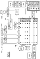
- Figure 1 shows a system on chip SOC comprising a plurality of master devices M and a plurality of slave devices S.
- the system on chip can also comprise at least one memory MEM, for example a flash memory, with a flash interface to communicate with the memory.
- the system on chip can also comprise instruction caches I-cache.
- the system on chip can also include a general-purpose direct memory access GPDMA1, different buses such as advanced high-performance buses AHB1, AHB4 and advanced peripheral buses APB, APB1, APB2, APB4.
- GPDMA1 general-purpose direct memory access
- different buses such as advanced high-performance buses AHB1, AHB4 and advanced peripheral buses APB, APB1, APB2, APB4.
- the system on chip can comprise different processing units as master devices M.
- the system on chip can comprise peripherals IP#1, ..., IP#6 as slave devices S.
- the peripherals can be organized in different domains PHD and sub-domains.
- the system on chip SOC also comprises different connection interfaces between the master devices and the slave devices.
- the system on chip comprises at least one bus matrix BM as a connection interface.
- the bus matrix BM is a connection interface that is connected on one side to the masters M and on the other side directly to the slave devices S or to a peripheral domain PHD.
- the bus matrix BM is configured to route the signals between the master devices M and either the slave devices S or the peripheral domains PHD so as to allow a communication between the master devices M and either the slave devices S or the peripheral domain PHD.
- the bus matrix BM is arranged in rows and columns. Each row is connected to one master port Mp0, ..., Mp N of the bus matrix BM. Each column is connected to one slave port Sp 0 ,..., Sp N of the bus matrix BM. In figure 1 , the connections between the rows and the columns are represented with dots.
- each slave S can communicate with different masters M, and each master M can communicate with different slaves S.
- the bus matrix BM is hard coded.
- a connection interface is also included in each peripheral domain PDM or sub-domain.
- Such a submatrix SM comprises on a first side a port connected to the bus matrix BM and on the other side a port connected to the peripherals or to the subdomains.
- Figure 2 illustrates an example of two connections of a bus matrix.
- the bus matrix is configured to connect a master device Mj to a slave device Sk, and to connect a master device My to the slave device Sk.
- the bus matrix comprises two slave ports Spj and Spy connected respectively to the master devices Mj et My, and a master port Mpk connected to the slave device Sk.
- the bus matrix also comprises an input stage ISBMj, ISBMy for each master device Mj, My connected to the bus matrix BM.
- Each input stage ISBMj, ISBMy is configured to register and hold an incoming transfer from the master device Mj, My connected to this input stage ISBMj, ISBMy.
- each input stage ISBMj, ISBMy is configured to hold the incoming transfer when the slave device Sk is busy.
- the bus matrix also comprises a decoder DBMjk, DBMyk, for each connection between a slave port Spj, Spy and a master port Mpk (ie. for each dot of the matrix).
- Each decoder is configured to select a slave device.
- the decoder implements a route table for each master device.
- the decoder is able to implement a remap mechanism and is further configured to route messages from the slave device connected to the decoder to the master.
- the bus matrix BM comprises an output stage for each slave device S connected to the bus matrix.
- the bus matrix comprises an output stage OSBMk connected to the master port My and the slave device Sk.
- the output stage OSBMk is connected to the decoders DBMjk and DBMyk and to all the other decoders DBMk of the row connected to the master port My.
- Each output stage includes an arbiter ABT, configured to determine which slave port has access to the shared slave device, and output logic OLBM.
- the output logic OLBM is configured to decide when to communicate with the master device selected by the arbiter.
- Figure 3 illustrates a connection of a submatrix SM.
- the submatrix is configured to connect one master device to different slave devices.
- the connection of the submatrix SM shown in figure 3 connects a master M to a slave device Sx.
- the submatrix comprises one slave port Sp connected to the master device M, and a master port Mpx connected to the slave device Sx.
- the submatrix SM comprises an input stage ISSM connected to a master port of the bus matrix.
- the input stage ISSM is configured to register and hold an incoming transfer from the bus matrix.
- the input stage ISSM is configured to hold the incoming transfer when the slave device S is busy.
- the submatrix SM also comprises a decoder DSMx, for each connection between an input stage ISSM and an output stage OSSMx of the submatrix SM.
- the decoder DSMx is configured to select a slave device and to implement a map table.
- Each output stage OSSMx includes an output logic OLSM.
- the output logic OLSM is configured to decide when to communicate with the master device.
- the bus matrix BM and each submatrix SM are configured to operate according to configuration parameters.
- the configuration parameters are used to define the operation of each input stage ISBM, ISSM.
- the configuration parameters can be used to disable a master device.
- the configuration parameters are also used to define the operation of each decoder DBM, DSM.
- the configuration parameters can define the route map and the remap table of the bus matrix BM or of the submatrix SM.
- the configuration parameters are also used to define the operation of each output stage OSBM, OSSM.
- the configuration parameters can be used to disable a slave device and to define the arbiter policy.
- the system on chip is configured to modify the configuration parameters so as to adapt the operation of the bus matrix and of each submatrix. This allows the versality of the system on chip improved.
- the system on chip SOC comprises default configuration parameters coded at a register-transfer level (i.e. RTL coded).
- the default configuration parameters define a default operation of the bus matrix and of each submatrix.
- the default operation of the bus matrix and of each submatrix is chosen when designing the system on chip.
- the default configuration parameters are chosen to guarantee the functionality of the bus matrix and of each submatrix in all possible scenarios. Nevertheless, the configuration parameters can be modified during runtime to improve the performance and the flexibility of the bus matrix and of each submatrix.
- each input stage ISBM, ISSM, each decoder DBM, DSM and each output stage OSBM, OSSM of the bus matrix BM and of each submatrix SM is connected to a configuration bus CFB.
- the configuration bus CFB is configured to deliver new configuration parameters to the bus matrix BM and to each submatrix SM.
- the new configuration parameters allow the operation of the bus matrix BM and of each submatrix SM to be modified and are stored in a memory MEM, such as a flash memory or a one-time programmable memory or a plurality of system configuration registers in a persistent domain.
- the flash memory is configured to include a flash memory area devoted to storage of the new configuration parameters.
- This flash memory area can be protected so that only an authorized user can access them and modify their values.
- the one-time programmable memory includes a memory area devoted to storage of the new configuration parameters for the connection interfaces. This memory area can also be protected
- some configuration system registers in a persistent domain are devoted to storage of the new configuration parameters for the connection interfaces.
- the bus matrix BM and each submatrix SM comprise selection circuits.
- Figures 4 and 5 illustrate different selection circuits SELC1, SELC2.
- the selection circuits are configured to select the configuration parameters between the default configuration parameters DCFP and the new configuration parameters NCFP.
- each element of the bus matrix and of each submatrix comprises such a selection circuit.
- each input stage ISBM, ISSM comprises a selection circuit SELC1 and/or SELC2 configured to select the configuration parameters of this input stage.
- Each decoder DBM, DSM also comprises a selection circuit configured to select the configuration parameters of this decoder.
- Each output stage also comprises a selection circuit configured to select the configuration parameters of this output stage.
- each selection circuit SELC1 comprises relevant parameter registers.
- the relevant parameter registers RPR1 are configured to store default configuration parameters DCFP coded at register-transfer level. These default parameters DCFP are associated to the element of the connection interface (i.e. the input stage, the decoder or the output stage) that includes the selection circuit SELC1.
- the relevant parameter registers RPR1 also comprise a volatile register CFVR1 connected to the configuration bus CFB and configured to store new configuration parameters NCFP received from the configuration bus CFG.
- system on chip can be configured to read the new configuration parameters NCFP stored in the memory MEM after a reset of the system on chip. Then, the system on chip can be configured to deliver the new configuration parameters to the volatile register CFVR1 through the configuration bus CFG.
- the volatile register CFVR1 can also be configured to store a guard bit GB1.
- the guard bit GB1 is configured to validate the possibility of using the new configuration parameters.
- the value of the guard bit GB1 is defined according to a value of an error-correcting code of the memory MEM after the reading of the new configuration parameters NCFP. In particular, if the error-correcting code indicates that the new configuration parameters are corrupted, the value of the guard bit GB1 is set to prevent using the new configuration parameters. If the error-correcting code indicates that the new configuration parameters are not corrupted, the value of the guard bit GB1 is set to allow using the new configuration parameters.
- the selection circuit SELC1 also comprises a multiplexer MUX1.
- the multiplexer MUX1 comprises two inputs configured to receive the default configuration parameters DCFP and the new configuration parameters NFCP and one output configured to deliver the selected configuration parameters SCFP.
- the multiplexer MUX1 also comprises a selector pin to select the configuration parameters between the default configuration parameters DCFP and the new configuration parameters NCFP.
- the selector pin is configured to receive a selection signal SEL1.
- the selection circuit SELC1 comprises an AND logic gate ANDG1 used to generate the selection signal SEL1.
- the logic gate ANDG1 is further configured to receive the guard bit GB, a reset signal RST1 and a disabling signal DSB1.
- the selection signal SELC1 is configured to select the new configuration parameters NCFP only when the guard bit GB1 indicates that the new configuration parameters NCFP are valid.
- the selection circuit SELC1 can be coded at a register-transfer level.
- another selection circuit SELC2 can also be used to gate signals SGT.
- the selection circuit SELC2 is configured to gate the signals SGT according to a gating bit SGB.
- the selection circuit SELC2 includes relevant parameter registers RPR2 storing a default gating bit DGB coded at a register-transfer level.
- the relevant parameter registers RPR2 also includes a volatile register CFVR2 connected to the configuration bus CFB.
- This volatile register CFVR2 is configured to store a new gating bit NGB received from the configuration bus CFB and can also be configured to store a guard bit GB2.
- the guard bit GB2 is configured to validate the possibility of using the new gating bit NGB.
- the selection circuit SELC2 further comprises an AND logic gate ANDG2 used to generate a selection signal SEL2.
- the logic gate ANDG2 is configured to receive the guard bit GB2, a reset signal RST2 and a disabling signal DSB2.
- the selection circuit SELC2 also comprises a multiplexer MUX2.
- the multiplexer MUX2 comprises two inputs configured to receive the default gating bit DGB and the new gating bit NGB and one output configured to deliver the selected gating bit SGB.
- the multiplexer MUX2 also comprises a selector pin configured to receive the selection signal SEL2.
- the selection signal SEL2 is configured to select the new gating bit NGB only when the guard bit GB2 indicates that the new gating bit NGB is valid.
- the selection circuit SELC2 also comprises an AND gate ANDG3 having a first input connected to the output of the multiplexer MUX2 to receive the selected gate bit SGB, and other inputs configured to receive the signals SGT to be gated. Therefore, the gate ANDG3 can gate the signals SGT according to the value of the selected gate bit SGB. These gated signals SGT can therefore be transmitted to a subcircuit SBC to be gated.
- such a selection circuit SELC2 is configured to gate signals SGT in order to enable or disable some features or parameters of the bus matrix BM or the submatrix SM.
Landscapes
- Engineering & Computer Science (AREA)
- Theoretical Computer Science (AREA)
- Computer Hardware Design (AREA)
- Physics & Mathematics (AREA)
- General Engineering & Computer Science (AREA)
- General Physics & Mathematics (AREA)
- Mathematical Physics (AREA)
- Software Systems (AREA)
- Microelectronics & Electronic Packaging (AREA)
- Computing Systems (AREA)
- Computer Networks & Wireless Communication (AREA)
- Information Transfer Systems (AREA)
- Stored Programmes (AREA)
- Bus Control (AREA)
- User Interface Of Digital Computer (AREA)
Abstract
According to an aspect, it is proposed a system on chip comprising:- at least one master device (Mj, My),- at least one slave device (Sk),- a connection interface (BM) configured to route signals between said at least one master device (Mj, My) and said at least one slave device (Sk), the connection interface being configured to operate according to configuration parameters,- a configuration bus (CFB) connected to the connection interface (BM), the configuration bus (CFB) being configured to deliver new configuration parameters to the connection interface so as to adapt the operation of the connection interface.
Description
- Embodiments of the present disclosure refers to a system on a chip (also known by the acronym "SoC"), and more particularly, to a connection interface between master devices and slave devices of the system on chip.
- A system on chip is an integrated electronic system configured to perform a plurality of functions. The system on chip can be used in an electronic device such as a microcontroller and can include a plurality of components. For example, the components can comprise at least one processing core, one or more volatile and non-volatile memories, for example a flash memory, and a plurality of peripherals. Some of the components are used as master devices, such as the processing core. Other components are used as slave devices, such as the peripherals.
- The components of the system on chip are interconnected via at least one connection interface (also called interconnection interface). For example, a connection interface can be a principal bus matrix or a connection interface inside a peripheral domain to address the different peripherals of the peripheral domain.
- Such connection interfaces are statically configured, for example in hard coded mode, so that, after a first initial configuration phase, the configuration of the bus matrix can no longer be changed.
- Therefore, by using such connection interfaces, the versatility of the system on chip is limited. In particular, the communication between the components of the system on chip cannot be adapted to specific applications.
- The problem therefore arises of providing a system on chip presenting improved versatility.
- According to an aspect, it is proposed a system on chip comprising:
- at least one master device,
- at least one slave device,
- a connection interface configured to route signals between said at least one master device and said at least one slave device, the connection interface being configured to operate according to configuration parameters, and
- a configuration bus connected to the connection interface, the configuration bus being configured to deliver new configuration parameters to the connection interface so as to adapt the operation of the connection interface.
- In such a system on chip, the operation of the connection interface can be modified with new configuration parameters.
- Therefore, the system on chip presents an improved versality of use, thanks to the possibility of modifying the operation of the connection interface.
- For example, such system on chip allows a route table and a remap table of the connection interface to be modified. The system on chip can also allow an arbiter policy of the connection interface to be modified so as to adapt the priorities between the master devices. The system on chip can also allow enabling or disabling the master devices and the slave devices.
- Advantageously, the connection interface comprises:
- at least one input stage connected to said at least one master device,
- at least one output stage connected to said at least one slave device,
- at least one decoder connected to said at least one input stage and to said at least one output stage.
- In particular, said at least one input stage, said at least one output stage and said at least one decoder are configured to operate according to said configuration parameters. More particularly, the configuration bus is connected to said at least one input stage, to said at least one output stage and to said at least one decoder and is configured to deliver to them the new configuration parameters so as to define their operation.
- Preferably, said at least one output stage includes an arbiter and an output logic circuit.
- According to a particularly advantageous embodiment, the system on chip comprises a memory connected to the configuration bus, the new configuration parameters being stored in said memory.
- According to a particularly advantageous embodiment, the system on chip comprises default configuration parameters coded at a register-transfer level.
- Preferably, the connection interface comprises a selection circuit configured to select the configuration parameters to apply amongst the new configuration parameters and the default configuration parameters.
- Advantageously, the selection circuit is configured to select the new configuration parameters to apply according to a value of a guard bit guarantying that the new configuration parameter is valid.
- Thus, the guard bit can be used to guarantee that a new configuration parameter is not corrupted.
- According to a particularly advantageous embodiment, the memory in which the new configuration parameters are stored is a flash memory.
- Alternatively, the new configuration parameters are stored is a one-time programmable memory.
- Alternatively, the new configuration parameters are stored in a plurality of system configuration registers. Such system configuration registers are in a persistent domain, i.e. they are powered with a battery in order to not lose information during standby.
- Other advantages and features of the invention will appear in the detailed description of embodiments and implementations, in no way restrictive, and the attached drawings in which:
- [
Fig 1 ] - [
Fig 2 ] - [
Fig 3 ] - [
Fig 4 ] - [
Fig 5 ] schematically illustrate various implementations and embodiments of the invention. -
Figure 1 shows a system on chip SOC comprising a plurality of master devices M and a plurality of slave devices S. The system on chip can also comprise at least one memory MEM, for example a flash memory, with a flash interface to communicate with the memory. The system on chip can also comprise instruction caches I-cache. - The system on chip can also include a general-purpose direct memory access GPDMA1, different buses such as advanced high-performance buses AHB1, AHB4 and advanced peripheral buses APB, APB1, APB2, APB4.
- For example, the system on chip can comprise different processing units as master devices M. The system on chip can comprise
peripherals IP# 1, ...,IP# 6 as slave devices S. The peripherals can be organized in different domains PHD and sub-domains. - The system on chip SOC also comprises different connection interfaces between the master devices and the slave devices. In particular, the system on chip comprises at least one bus matrix BM as a connection interface. The bus matrix BM is a connection interface that is connected on one side to the masters M and on the other side directly to the slave devices S or to a peripheral domain PHD.
- The bus matrix BM is configured to route the signals between the master devices M and either the slave devices S or the peripheral domains PHD so as to allow a communication between the master devices M and either the slave devices S or the peripheral domain PHD.
- The bus matrix BM is arranged in rows and columns. Each row is connected to one master port Mp0, ..., MpN of the bus matrix BM. Each column is connected to one slave port Sp0,..., SpN of the bus matrix BM. In
figure 1 , the connections between the rows and the columns are represented with dots. - According to the connections defined by the bus matrix, each slave S can communicate with different masters M, and each master M can communicate with different slaves S. The bus matrix BM is hard coded.
- A connection interface, named submatrix SM, is also included in each peripheral domain PDM or sub-domain. Such a submatrix SM comprises on a first side a port connected to the bus matrix BM and on the other side a port connected to the peripherals or to the subdomains.
-
Figure 2 illustrates an example of two connections of a bus matrix. In particular, the bus matrix is configured to connect a master device Mj to a slave device Sk, and to connect a master device My to the slave device Sk. Thus, the bus matrix comprises two slave ports Spj and Spy connected respectively to the master devices Mj et My, and a master port Mpk connected to the slave device Sk. - The bus matrix also comprises an input stage ISBMj, ISBMy for each master device Mj, My connected to the bus matrix BM. Each input stage ISBMj, ISBMy is configured to register and hold an incoming transfer from the master device Mj, My connected to this input stage ISBMj, ISBMy. In particular, each input stage ISBMj, ISBMy is configured to hold the incoming transfer when the slave device Sk is busy.
- The bus matrix also comprises a decoder DBMjk, DBMyk, for each connection between a slave port Spj, Spy and a master port Mpk (ie. for each dot of the matrix). Each decoder is configured to select a slave device. In particular, the decoder implements a route table for each master device. The decoder is able to implement a remap mechanism and is further configured to route messages from the slave device connected to the decoder to the master.
- The bus matrix BM comprises an output stage for each slave device S connected to the bus matrix. For example, in
figure 2 , the bus matrix comprises an output stage OSBMk connected to the master port My and the slave device Sk. The output stage OSBMk is connected to the decoders DBMjk and DBMyk and to all the other decoders DBMk of the row connected to the master port My. - Each output stage includes an arbiter ABT, configured to determine which slave port has access to the shared slave device, and output logic OLBM. The output logic OLBM is configured to decide when to communicate with the master device selected by the arbiter.
-
Figure 3 illustrates a connection of a submatrix SM. The submatrix is configured to connect one master device to different slave devices. For example, the connection of the submatrix SM shown infigure 3 connects a master M to a slave device Sx. Thus, for each connection, the submatrix comprises one slave port Sp connected to the master device M, and a master port Mpx connected to the slave device Sx. - The submatrix SM comprises an input stage ISSM connected to a master port of the bus matrix. The input stage ISSM is configured to register and hold an incoming transfer from the bus matrix. In particular, the input stage ISSM is configured to hold the incoming transfer when the slave device S is busy.
- The submatrix SM also comprises a decoder DSMx, for each connection between an input stage ISSM and an output stage OSSMx of the submatrix SM. The decoder DSMx is configured to select a slave device and to implement a map table.
- Each output stage OSSMx includes an output logic OLSM. The output logic OLSM is configured to decide when to communicate with the master device.
- The bus matrix BM and each submatrix SM are configured to operate according to configuration parameters. For example, the configuration parameters are used to define the operation of each input stage ISBM, ISSM. In particular, the configuration parameters can be used to disable a master device.
- The configuration parameters are also used to define the operation of each decoder DBM, DSM. In particular, the configuration parameters can define the route map and the remap table of the bus matrix BM or of the submatrix SM.
- The configuration parameters are also used to define the operation of each output stage OSBM, OSSM. In particular, the configuration parameters can be used to disable a slave device and to define the arbiter policy.
- The system on chip is configured to modify the configuration parameters so as to adapt the operation of the bus matrix and of each submatrix. This allows the versality of the system on chip improved.
- More particularly, the system on chip SOC comprises default configuration parameters coded at a register-transfer level (i.e. RTL coded). The default configuration parameters define a default operation of the bus matrix and of each submatrix. The default operation of the bus matrix and of each submatrix is chosen when designing the system on chip. In particular, the default configuration parameters are chosen to guarantee the functionality of the bus matrix and of each submatrix in all possible scenarios. Nevertheless, the configuration parameters can be modified during runtime to improve the performance and the flexibility of the bus matrix and of each submatrix.
- Indeed, as shown in
figures 1 and2 , the bus matrix BM and each submatrix SM are connected to a configuration bus. More particularly, each input stage ISBM, ISSM, each decoder DBM, DSM and each output stage OSBM, OSSM of the bus matrix BM and of each submatrix SM is connected to a configuration bus CFB. - The configuration bus CFB is configured to deliver new configuration parameters to the bus matrix BM and to each submatrix SM. The new configuration parameters allow the operation of the bus matrix BM and of each submatrix SM to be modified and are stored in a memory MEM, such as a flash memory or a one-time programmable memory or a plurality of system configuration registers in a persistent domain.
- In particular, the flash memory is configured to include a flash memory area devoted to storage of the new configuration parameters. This flash memory area can be protected so that only an authorized user can access them and modify their values.
- Alternatively, the one-time programmable memory includes a memory area devoted to storage of the new configuration parameters for the connection interfaces. This memory area can also be protected
- Alternatively, some configuration system registers in a persistent domain are devoted to storage of the new configuration parameters for the connection interfaces.
- The bus matrix BM and each submatrix SM comprise selection circuits.
Figures 4 and5 illustrate different selection circuits SELC1, SELC2. - The selection circuits are configured to select the configuration parameters between the default configuration parameters DCFP and the new configuration parameters NCFP. In particular, each element of the bus matrix and of each submatrix comprises such a selection circuit.
- More particularly, each input stage ISBM, ISSM comprises a selection circuit SELC1 and/or SELC2 configured to select the configuration parameters of this input stage.
- Each decoder DBM, DSM also comprises a selection circuit configured to select the configuration parameters of this decoder.
- Each output stage also comprises a selection circuit configured to select the configuration parameters of this output stage.
- As shown in
figure 4 , each selection circuit SELC1 comprises relevant parameter registers. - The relevant parameter registers RPR1 are configured to store default configuration parameters DCFP coded at register-transfer level. These default parameters DCFP are associated to the element of the connection interface (i.e. the input stage, the decoder or the output stage) that includes the selection circuit SELC1.
- The relevant parameter registers RPR1 also comprise a volatile register CFVR1 connected to the configuration bus CFB and configured to store new configuration parameters NCFP received from the configuration bus CFG.
- In particular, the system on chip can be configured to read the new configuration parameters NCFP stored in the memory MEM after a reset of the system on chip. Then, the system on chip can be configured to deliver the new configuration parameters to the volatile register CFVR1 through the configuration bus CFG.
- The volatile register CFVR1 can also be configured to store a guard bit GB1. The guard bit GB1 is configured to validate the possibility of using the new configuration parameters. The value of the guard bit GB1 is defined according to a value of an error-correcting code of the memory MEM after the reading of the new configuration parameters NCFP. In particular, if the error-correcting code indicates that the new configuration parameters are corrupted, the value of the guard bit GB1 is set to prevent using the new configuration parameters. If the error-correcting code indicates that the new configuration parameters are not corrupted, the value of the guard bit GB1 is set to allow using the new configuration parameters.
- The selection circuit SELC1 also comprises a multiplexer MUX1. The multiplexer MUX1 comprises two inputs configured to receive the default configuration parameters DCFP and the new configuration parameters NFCP and one output configured to deliver the selected configuration parameters SCFP.
- The multiplexer MUX1 also comprises a selector pin to select the configuration parameters between the default configuration parameters DCFP and the new configuration parameters NCFP. The selector pin is configured to receive a selection signal SEL1.
- In particular, the selection circuit SELC1 comprises an AND logic gate ANDG1 used to generate the selection signal SEL1. The logic gate ANDG1 is further configured to receive the guard bit GB, a reset signal RST1 and a disabling signal DSB1. Thus, the selection signal SELC1 is configured to select the new configuration parameters NCFP only when the guard bit GB1 indicates that the new configuration parameters NCFP are valid. The selection circuit SELC1 can be coded at a register-transfer level.
- As shown in
figure 5 , another selection circuit SELC2 can also be used to gate signals SGT. The selection circuit SELC2 is configured to gate the signals SGT according to a gating bit SGB. - More particularly, the selection circuit SELC2 includes relevant parameter registers RPR2 storing a default gating bit DGB coded at a register-transfer level. The relevant parameter registers RPR2 also includes a volatile register CFVR2 connected to the configuration bus CFB. This volatile register CFVR2 is configured to store a new gating bit NGB received from the configuration bus CFB and can also be configured to store a guard bit GB2. The guard bit GB2 is configured to validate the possibility of using the new gating bit NGB.
- The selection circuit SELC2 further comprises an AND logic gate ANDG2 used to generate a selection signal SEL2. The logic gate ANDG2 is configured to receive the guard bit GB2, a reset signal RST2 and a disabling signal DSB2.
- The selection circuit SELC2 also comprises a multiplexer MUX2. The multiplexer MUX2 comprises two inputs configured to receive the default gating bit DGB and the new gating bit NGB and one output configured to deliver the selected gating bit SGB. The multiplexer MUX2 also comprises a selector pin configured to receive the selection signal SEL2. Thus, the selection signal SEL2 is configured to select the new gating bit NGB only when the guard bit GB2 indicates that the new gating bit NGB is valid.
- The selection circuit SELC2 also comprises an AND gate ANDG3 having a first input connected to the output of the multiplexer MUX2 to receive the selected gate bit SGB, and other inputs configured to receive the signals SGT to be gated. Therefore, the gate ANDG3 can gate the signals SGT according to the value of the selected gate bit SGB. These gated signals SGT can therefore be transmitted to a subcircuit SBC to be gated.
- Thus, such a selection circuit SELC2 is configured to gate signals SGT in order to enable or disable some features or parameters of the bus matrix BM or the submatrix SM.
Claims (10)
- System on chip comprising:- at least one master device (Mj, My, M),- at least one slave device (Sk, Sx),- a connection interface (BM, SM) configured to route signals between said at least one master device (Mj, My, M) and said at least one slave device (Sk, Sx), the connection interface being configured to operate according to configuration parameters, and- a configuration bus (CFB) connected to the connection interface (BM, SM), the configuration bus (CFB) being configured to deliver new configuration parameters to the connection interface so as to adapt the operation of the connection interface.
- System on chip according to claim 1, in which the connection interface comprises:- at least one input stage (ISBM, ISSM) connected to said at least one master device (Mj, My, M),- at least one output stage (OSBM, OSSM) connected to said at least one slave device (Sk, Sx),- at least one decoder (DBM, DSM) connected to said at least one input stage (ISBM, ISSM) and to said at least one output stage (OSBM, OSSM),
in which said at least one input stage (ISBM, ISSM), said at least one output stage (OSBM, OSSM) and said at least one decoder (DBM, DSM) are configured to operate according to said configuration parameters, and in which the configuration bus (CFB) is connected to said at least one input stage (ISBM, ISSM), to said at least one output stage (OSBM, OSSM) and to said at least one decoder (DBM, DSM) and is configured to deliver to them the new configuration parameters so as to define their operation. - System on chip according to claim 2, in which said at least one output stage (OSBM, OSSM) includes an arbiter and an output logic circuit (OLBM, OLSM).
- System on chip according to one of claims 1 to 3, comprising a memory (MEM) connected to the configuration bus, the new configuration parameters being stored in said memory.
- System on chip according to one of claims 1 to 4, comprising default configuration parameters (DCFP) coded at a register-transfer level.
- System on chip according to claim 5, in which the connection interface comprises a selection circuit (SELC) configured to select the configuration parameters to apply between the new configuration parameters and the default configuration parameters.
- System on chip according to claim 6, in which the selection circuit (SELC) is configured to select the new configuration parameter (NCFP) to apply according to a value of a guard bit (GB) guarantying that the new configuration parameter (NCFP) is valid.
- System on chip according to one of claims 1 to 7, in which the memory in which the new configuration parameters are stored is a flash memory.
- System on chip according to one of claims 1 to 7, in which the memory in which the new configuration parameters are stored is a one-time programmable memory.
- System on chip according to one of claims 1 to 7, in which the memory in which the new configuration parameters are stored is a plurality of system configuration registers.
Applications Claiming Priority (1)
| Application Number | Priority Date | Filing Date | Title |
|---|---|---|---|
| FR2106544A FR3124284B1 (en) | 2021-06-21 | 2021-06-21 | System-on-chip including a connection interface between master devices and slave devices |
Publications (1)
| Publication Number | Publication Date |
|---|---|
| EP4109286A1 true EP4109286A1 (en) | 2022-12-28 |
Family
ID=77411840
Family Applications (1)
| Application Number | Title | Priority Date | Filing Date |
|---|---|---|---|
| EP22178614.8A Pending EP4109286A1 (en) | 2021-06-21 | 2022-06-13 | System on chip comprising a connection interface between master devices and slave devices |
Country Status (4)
| Country | Link |
|---|---|
| US (1) | US12135679B2 (en) |
| EP (1) | EP4109286A1 (en) |
| CN (1) | CN115576874A (en) |
| FR (1) | FR3124284B1 (en) |
Citations (2)
| Publication number | Priority date | Publication date | Assignee | Title |
|---|---|---|---|---|
| US20080294806A1 (en) * | 2007-04-17 | 2008-11-27 | Cypress Semiconductor Corporation | Programmable system-on-chip hub |
| US20200174964A1 (en) * | 2018-11-29 | 2020-06-04 | Stmicroelectronics (Rousset) Sas | Management of access restriction within a system on chip |
Family Cites Families (7)
| Publication number | Priority date | Publication date | Assignee | Title |
|---|---|---|---|---|
| WO2006030650A1 (en) * | 2004-09-16 | 2006-03-23 | Nec Corporation | Information processing device having a plurality of processing units sharing a resource |
| KR101076869B1 (en) * | 2010-03-16 | 2011-10-25 | 광운대학교 산학협력단 | Memory centric communication apparatus in coarse grained reconfigurable array |
| US11321263B2 (en) * | 2014-12-17 | 2022-05-03 | Intel Corporation | High bandwidth core to network-on-chip interface |
| CN104598407B (en) * | 2015-02-03 | 2018-11-30 | 杭州士兰控股有限公司 | System on chip and control method |
| WO2016184525A1 (en) * | 2015-05-21 | 2016-11-24 | Projoule Gmbh | Apparatus and method for configuring a microcontroller system |
| KR20180062807A (en) * | 2016-12-01 | 2018-06-11 | 삼성전자주식회사 | System interconnect and system on chip having the same |
| CN112286863B (en) * | 2020-11-18 | 2023-08-18 | 合肥沛睿微电子股份有限公司 | Processing and memory circuit |
-
2021
- 2021-06-21 FR FR2106544A patent/FR3124284B1/en active Active
-
2022
- 2022-06-08 US US17/835,746 patent/US12135679B2/en active Active
- 2022-06-13 EP EP22178614.8A patent/EP4109286A1/en active Pending
- 2022-06-21 CN CN202210707646.8A patent/CN115576874A/en active Pending
Patent Citations (2)
| Publication number | Priority date | Publication date | Assignee | Title |
|---|---|---|---|---|
| US20080294806A1 (en) * | 2007-04-17 | 2008-11-27 | Cypress Semiconductor Corporation | Programmable system-on-chip hub |
| US20200174964A1 (en) * | 2018-11-29 | 2020-06-04 | Stmicroelectronics (Rousset) Sas | Management of access restriction within a system on chip |
Also Published As
| Publication number | Publication date |
|---|---|
| FR3124284B1 (en) | 2024-04-19 |
| FR3124284A1 (en) | 2022-12-23 |
| CN115576874A (en) | 2023-01-06 |
| US20220405232A1 (en) | 2022-12-22 |
| US12135679B2 (en) | 2024-11-05 |
Similar Documents
| Publication | Publication Date | Title |
|---|---|---|
| US8572297B2 (en) | Programmable system-on-chip hub | |
| EP0840455B1 (en) | A microcontroller accessible macrocell | |
| US5686844A (en) | Integrated circuit pins configurable as a clock input pin and as a digital I/O pin or as a device reset pin and as a digital I/O pin and method therefor | |
| US5864505A (en) | Random access memory with plural simultaneously operable banks | |
| JP3853736B2 (en) | User configurable on-chip memory system | |
| US9537488B1 (en) | Apparatus for configurable interface and associated methods | |
| US8239663B2 (en) | System and method for maintaining the security of memory contents and computer architecture employing the same | |
| US9092322B2 (en) | Processor system and control method thereof | |
| KR20060002851A (en) | Memory Management in Data Processing Systems | |
| US7234011B2 (en) | Advanced microcontroller bus architecture (AMBA) system with reduced power consumption and method of driving AMBA system | |
| US20130031290A1 (en) | System and Method for Implementing a Secure Processor Data Bus | |
| KR100814904B1 (en) | On-Chip Communication architecture | |
| US20080244131A1 (en) | Architecture for configurable bus arbitration in multibus systems with customizable master and slave circuits | |
| US12135679B2 (en) | System on chip including a reconfigurable connection interface between master devices and slave devices | |
| US6901490B2 (en) | Read/modify/write registers | |
| RU2108619C1 (en) | Microcomputer | |
| US20150178008A1 (en) | Register configuration | |
| JPH05189296A (en) | Simultaneous writing access device for single-bit memory | |
| JP3296184B2 (en) | Semiconductor integrated circuit | |
| US12536342B2 (en) | SOC architecture with secure, selective peripheral enabling/disabling | |
| EP4571751A1 (en) | Partitioned non-volatile memory (nvm) having a normal read bus and a verify read bus | |
| JP6493044B2 (en) | Multiprocessor system | |
| SU746488A1 (en) | Interface | |
| US8924672B2 (en) | Device with processing unit and information storage | |
| JP3310482B2 (en) | Microcomputer |
Legal Events
| Date | Code | Title | Description |
|---|---|---|---|
| PUAI | Public reference made under article 153(3) epc to a published international application that has entered the european phase |
Free format text: ORIGINAL CODE: 0009012 |
|
| STAA | Information on the status of an ep patent application or granted ep patent |
Free format text: STATUS: REQUEST FOR EXAMINATION WAS MADE |
|
| 17P | Request for examination filed |
Effective date: 20220613 |
|
| AK | Designated contracting states |
Kind code of ref document: A1 Designated state(s): AL AT BE BG CH CY CZ DE DK EE ES FI FR GB GR HR HU IE IS IT LI LT LU LV MC MK MT NL NO PL PT RO RS SE SI SK SM TR |
|
| STAA | Information on the status of an ep patent application or granted ep patent |
Free format text: STATUS: EXAMINATION IS IN PROGRESS |