EP4106199A1 - Dispositif de sélection de tension d'alimentation avec commutations contrôlées en tension et en courant - Google Patents
Dispositif de sélection de tension d'alimentation avec commutations contrôlées en tension et en courant Download PDFInfo
- Publication number
- EP4106199A1 EP4106199A1 EP22178474.7A EP22178474A EP4106199A1 EP 4106199 A1 EP4106199 A1 EP 4106199A1 EP 22178474 A EP22178474 A EP 22178474A EP 4106199 A1 EP4106199 A1 EP 4106199A1
- Authority
- EP
- European Patent Office
- Prior art keywords
- circuit
- transistor
- node
- supply voltage
- voltage
- Prior art date
- Legal status (The legal status is an assumption and is not a legal conclusion. Google has not performed a legal analysis and makes no representation as to the accuracy of the status listed.)
- Granted
Links
Images







Classifications
-
- H—ELECTRICITY
- H03—ELECTRONIC CIRCUITRY
- H03K—PULSE TECHNIQUE
- H03K17/00—Electronic switching or gating, i.e. not by contact-making and –breaking
- H03K17/16—Modifications for eliminating interference voltages or currents
- H03K17/161—Modifications for eliminating interference voltages or currents in field-effect transistor switches
- H03K17/162—Modifications for eliminating interference voltages or currents in field-effect transistor switches without feedback from the output circuit to the control circuit
-
- H—ELECTRICITY
- H03—ELECTRONIC CIRCUITRY
- H03K—PULSE TECHNIQUE
- H03K17/00—Electronic switching or gating, i.e. not by contact-making and –breaking
- H03K17/51—Electronic switching or gating, i.e. not by contact-making and –breaking characterised by the components used
- H03K17/56—Electronic switching or gating, i.e. not by contact-making and –breaking characterised by the components used by the use, as active elements, of semiconductor devices
- H03K17/687—Electronic switching or gating, i.e. not by contact-making and –breaking characterised by the components used by the use, as active elements, of semiconductor devices the devices being field-effect transistors
- H03K17/693—Switching arrangements with several input- or output-terminals, e.g. multiplexers, distributors
-
- G—PHYSICS
- G05—CONTROLLING; REGULATING
- G05F—SYSTEMS FOR REGULATING ELECTRIC OR MAGNETIC VARIABLES
- G05F1/00—Automatic systems in which deviations of an electric quantity from one or more predetermined values are detected at the output of the system and fed back to a device within the system to restore the detected quantity to its predetermined value or values, i.e. retroactive systems
- G05F1/10—Regulating voltage or current
- G05F1/46—Regulating voltage or current wherein the variable actually regulated by the final control device is DC
-
- G—PHYSICS
- G05—CONTROLLING; REGULATING
- G05F—SYSTEMS FOR REGULATING ELECTRIC OR MAGNETIC VARIABLES
- G05F1/00—Automatic systems in which deviations of an electric quantity from one or more predetermined values are detected at the output of the system and fed back to a device within the system to restore the detected quantity to its predetermined value or values, i.e. retroactive systems
- G05F1/10—Regulating voltage or current
- G05F1/46—Regulating voltage or current wherein the variable actually regulated by the final control device is DC
- G05F1/56—Regulating voltage or current wherein the variable actually regulated by the final control device is DC using semiconductor devices in series with the load as final control devices
- G05F1/59—Regulating voltage or current wherein the variable actually regulated by the final control device is DC using semiconductor devices in series with the load as final control devices including plural semiconductor devices as final control devices for a single load
-
- G—PHYSICS
- G06—COMPUTING OR CALCULATING; COUNTING
- G06F—ELECTRIC DIGITAL DATA PROCESSING
- G06F1/00—Details not covered by groups G06F3/00 - G06F13/00 and G06F21/00
- G06F1/26—Power supply means, e.g. regulation thereof
- G06F1/263—Arrangements for using multiple switchable power supplies, e.g. battery and AC
-
- H—ELECTRICITY
- H03—ELECTRONIC CIRCUITRY
- H03K—PULSE TECHNIQUE
- H03K17/00—Electronic switching or gating, i.e. not by contact-making and –breaking
- H03K17/002—Switching arrangements with several input- or output terminals
-
- H—ELECTRICITY
- H03—ELECTRONIC CIRCUITRY
- H03K—PULSE TECHNIQUE
- H03K17/00—Electronic switching or gating, i.e. not by contact-making and –breaking
- H03K17/002—Switching arrangements with several input- or output terminals
- H03K17/005—Switching arrangements with several input- or output terminals with several inputs only
-
- H—ELECTRICITY
- H03—ELECTRONIC CIRCUITRY
- H03K—PULSE TECHNIQUE
- H03K17/00—Electronic switching or gating, i.e. not by contact-making and –breaking
- H03K17/16—Modifications for eliminating interference voltages or currents
- H03K17/161—Modifications for eliminating interference voltages or currents in field-effect transistor switches
-
- H—ELECTRICITY
- H03—ELECTRONIC CIRCUITRY
- H03K—PULSE TECHNIQUE
- H03K17/00—Electronic switching or gating, i.e. not by contact-making and –breaking
- H03K17/28—Modifications for introducing a time delay before switching
- H03K17/284—Modifications for introducing a time delay before switching in field effect transistor switches
-
- H—ELECTRICITY
- H03—ELECTRONIC CIRCUITRY
- H03K—PULSE TECHNIQUE
- H03K17/00—Electronic switching or gating, i.e. not by contact-making and –breaking
- H03K17/30—Modifications for providing a predetermined threshold before switching
- H03K17/302—Modifications for providing a predetermined threshold before switching in field-effect transistor switches
-
- H—ELECTRICITY
- H03—ELECTRONIC CIRCUITRY
- H03K—PULSE TECHNIQUE
- H03K19/00—Logic circuits, i.e. having at least two inputs acting on one output; Inverting circuits
- H03K19/0008—Arrangements for reducing power consumption
- H03K19/0016—Arrangements for reducing power consumption by using a control or a clock signal, e.g. in order to apply power supply
-
- H—ELECTRICITY
- H02—GENERATION; CONVERSION OR DISTRIBUTION OF ELECTRIC POWER
- H02J—ELECTRIC POWER NETWORKS; CIRCUIT ARRANGEMENTS OR SYSTEMS FOR SUPPLYING OR DISTRIBUTING ELECTRIC POWER; SYSTEMS FOR STORING ELECTRIC ENERGY
- H02J1/00—Circuit arrangements for DC mains or DC distribution networks
- H02J1/08—Three-wire DC power distribution systems; Systems having more than three wires
- H02J1/082—DC supplies with two or more different DC voltage levels
-
- H—ELECTRICITY
- H02—GENERATION; CONVERSION OR DISTRIBUTION OF ELECTRIC POWER
- H02J—ELECTRIC POWER NETWORKS; CIRCUIT ARRANGEMENTS OR SYSTEMS FOR SUPPLYING OR DISTRIBUTING ELECTRIC POWER; SYSTEMS FOR STORING ELECTRIC ENERGY
- H02J1/00—Circuit arrangements for DC mains or DC distribution networks
- H02J1/08—Three-wire DC power distribution systems; Systems having more than three wires
- H02J1/084—Three-wire DC power distribution systems; Systems having more than three wires for selectively connecting the load or loads to one or several among a plurality of power lines or power sources
-
- H—ELECTRICITY
- H02—GENERATION; CONVERSION OR DISTRIBUTION OF ELECTRIC POWER
- H02J—ELECTRIC POWER NETWORKS; CIRCUIT ARRANGEMENTS OR SYSTEMS FOR SUPPLYING OR DISTRIBUTING ELECTRIC POWER; SYSTEMS FOR STORING ELECTRIC ENERGY
- H02J2105/00—Networks for supplying or distributing electric power characterised by their spatial reach or by the load
- H02J2105/40—Networks for supplying or distributing electric power characterised by their spatial reach or by the load characterised by the loads connecting to the networks or being supplied by the networks
-
- H—ELECTRICITY
- H03—ELECTRONIC CIRCUITRY
- H03K—PULSE TECHNIQUE
- H03K2217/00—Indexing scheme related to electronic switching or gating, i.e. not by contact-making or -breaking covered by H03K17/00
- H03K2217/0081—Power supply means, e.g. to the switch driver
-
- Y—GENERAL TAGGING OF NEW TECHNOLOGICAL DEVELOPMENTS; GENERAL TAGGING OF CROSS-SECTIONAL TECHNOLOGIES SPANNING OVER SEVERAL SECTIONS OF THE IPC; TECHNICAL SUBJECTS COVERED BY FORMER USPC CROSS-REFERENCE ART COLLECTIONS [XRACs] AND DIGESTS
- Y02—TECHNOLOGIES OR APPLICATIONS FOR MITIGATION OR ADAPTATION AGAINST CLIMATE CHANGE
- Y02D—CLIMATE CHANGE MITIGATION TECHNOLOGIES IN INFORMATION AND COMMUNICATION TECHNOLOGIES [ICT], I.E. INFORMATION AND COMMUNICATION TECHNOLOGIES AIMING AT THE REDUCTION OF THEIR OWN ENERGY USE
- Y02D10/00—Energy efficient computing, e.g. low power processors, power management or thermal management
Definitions
- the present invention relates to the field of electronic circuits with several supply voltages and more particularly to a supply voltage selection circuit for a multi-core integrated circuit.
- this modification of the level of the supply voltage must be able to be done dynamically, without interrupting the operation of the integrated circuit.
- the dynamic management of the level of the supply voltage is essential in the case of high performance computing circuits HPC (acronym of the expression High Performance Computing).
- HPC high performance computing circuits
- New high-performance computing processor architectures are usually split into multiple cores. We are talking in the case of multi-core processors.
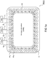
- the picture 1a illustrates a diagram of an exemplary electronic circuit comprising a plurality of cores with supply voltage management.
- the example includes three sources of supply voltages by way of illustration and not limitation.
- the electronic circuit illustrated is a multi-core processor PROC comprising a plurality of supply voltage sources VDD H VDD M and VDD L such that VDD H ⁇ VDD M ⁇ VDD L ; N CORE calculation cores ⁇ and M supply voltage selector circuits VSi, with N a natural integer greater than 1 and i a natural integer from 1 to N and with M a natural integer greater than 1 and j a natural integer from 1 to M.
- Each voltage selector circuit VS j is configured to supply to at least one calculation core CORE i , a supply voltage chosen from among VDD H VDD M VDD L . . CORE i cores operate at different frequencies. The workloads at the output of each CORE ⁇ core change dynamically as the calculations are performed.
- the supply voltage determines the computing power and energy cost of logical operations. Indeed, a calculation core operating in full calculation mode must be supplied by the maximum voltage VDD H ; a calculation core operating during an average calculation activity can be powered by the average voltage VDD M ; and a sleeping computing core requires only the minimum voltage VDD L .
- the quantity of calculation operations to be carried out and the algorithmic process used by each CORE ⁇ core determine the means of calculation required and thus the supply voltage required for said core in real time.
- the supply voltage of said core must be adjusted to minimize the product of calculation time by energy consumption, this technique is called dynamic voltage adjustment. scaling). It is particularly interesting not to interrupt the activity of the heart during the transitions between two power levels.
- the voltage selector circuits VS j make it possible to implement dynamic management of the supply voltage for a large number N of cores CORE i (N>10).
- the N calculation cores CORE ⁇ and M supply voltage selector circuits VS j are implemented on the same IC chip and the sources of supply voltages VDD H VDD M and VDD L are external to the IC chip.
- the supply voltages VDD H VDD M and VDD L are respectively propagated to the IC chip via the common supply rails R H , R M and R L .
- the common supply rails being made via conductive materials always exhibit parasitic inductive (or self-induction) effects presented here by the parasitic inductances L H , L M and L L .
- the power disturbance experienced by a compute core generates computation errors.
- the working frequency of a core has been designed to be compatible with a supply voltage value which is a priori fixed. Disturbances due to the self-induction phenomenon will thus create an incompatibility between the supply voltage and the working frequency of the computing core.
- Timing diagram 1c.1 illustrates the time variation of voltage VCORE 1 which supplies calculation core CORE 1 chosen by voltage selection circuit VS 1 .
- the timing diagram 1c.2 illustrates the temporal variation of the voltage VCORE 2 which supplies the calculation core CORE 2 chosen by the voltage selection circuit VS 2 .
- the timing diagram 1c.3 illustrates, more generally, the temporal variation of the voltage VCORE n which supplies any computing core CORE n chosen by the associated voltage selection circuit VS n .
- the voltage VCORE 1 is configured to remain constant at the medium voltage level VDD M
- the voltage VCORE 2 is configured to make a downward transition from the high voltage level VDD H to the medium voltage level VDD M
- the voltage VCORE N is configured to make a rising transition from the low voltage level VDD L to the medium voltage level VDD M . Sudden and simultaneous switchings cause high current inrushes in the parasitic inductances L M , L L and L H in a reduced time interval. Thus, the transitions carried out to change the supply of the core CORE 2 and of the core CORE N disturb the common rail R M of the average supply voltage level VDD M .
- This disturbance is observable on all power nodes VCORE 1 VCORE 2 up to VCORE N .
- a disturbance in the form of a power drop is observed on the power supply node VCORE 1 which is normally configured to remain constant at the average voltage level VDD M .
- VDD M the average voltage level
- the technical problem to be solved is then to develop supply voltage selection circuits allowing the dynamic adjustment of the voltage while limiting the switching noise due to the parasitic inductive effect of the common supply rails and avoiding the phenomenon of reverse currents in said common rails.
- the European patent EP3267583B1 proposes a supply voltage selection circuit architecture for controlling the voltage shape on the supply rail of a computing core circuit during the transition from one supply voltage level to another level.
- the drawback of the solution proposed by the aforementioned patent is that it is limited to voltage control and does not take into account the high current surges on each common rail. Current variations are not controlled and the problem of switching noise resulting from parasitic inductances is not solved.
- the US patent US10439602B2 proposes a supply voltage selection circuit architecture making it possible to switch between two supply rails, one main and one auxiliary, depending on the voltage available. If the main voltage becomes lower than a defined threshold, the auxiliary voltage is used to regulate the output voltage and restore it to the desired level.
- the drawback of the solution proposed by the aforementioned patent consists in that the operation of the solution requires maintaining the main and auxiliary source power switches in the on state simultaneously. This generates reverse currents in the circuit reducing the computational and energy performance of the circuit.
- the solution proposed by the aforementioned patent requires the implementation of four comparators in order to detect the states of the two rails and the permanent operation of at least two comparators. This considerably increases the energy consumption of the supply voltage selection circuit.
- the US patent US10432184B1 proposes a power supply voltage selection circuit architecture comprising a current multiplexer making it possible to produce smooth transitions in order to limit current draws.
- the drawback of the solution proposed by the aforementioned patent consists in that it requires the implementation of a capacitive element having a large capacity. This induces a considerable increase in the area occupied by the device as a whole and then poses hardware integration constraints.
- the solution proposed by the patent shows very long transition times making it incompatible with applications operating at high frequency.
- European patent application EP3734398A1 proposes a supply voltage selection circuit architecture using a single input supply rail to provide a main voltage and a configurable voltage simultaneously.
- the drawback of the solution proposed by the aforementioned patent consists in that it requires permanent operation of a comparator, which considerably increases the energy consumption of the supply voltage selection circuit.
- the solution of the patent application does not take into account the high current surges on each common rail. Current variations are not controlled and the problem of switching noise due to parasitic inductances is not solved.
- the invention proposes different embodiments of a selection circuit architecture making it possible to perform rising and/or falling transitions according to slow and fast phase sequencing sets so as to solve at the same time the problems of inductive switching noise and the problems of currents in the power rails.
- This solution has several advantages related to the ease of implementation and the flexibility of possible configurations to adapt to specific constraints when designing the circuit.
- the absolute value of the first slope is between one tenth of the absolute value of the second slope and one fifth of the absolute value of the second slope.
- the first linear regulation circuit is configured to control the first transistor in linear mode via the slaving of the output supply voltage on the voltage ramp applied to the second input node when the first switch is on.
- the first transition management circuit further comprises a first gradual transition circuit having an output node connected to the gate of the first transistor through a second switch, the first gradual transition circuit being capable of applying a control signal having a gradual variation to the gate of the second transistor when the second switch is on.
- the second transition management circuit comprises a second gradual transition circuit having an output node connected to the gate of the second transistor through a fourth switch, said gradual transition circuit being capable of applying a control signal on the gate of the second transistor when the third switch is on; said control signal exhibiting a gradual increasing or decreasing variation.
- the configuration circuit further comprises a circuit for comparing the output supply voltage with a predetermined threshold.
- the configuration circuit further comprises a circuit for generating a predetermined duration.
- the picture 1a illustrates a diagram of an exemplary electronic circuit comprising a plurality of cores with supply voltage management.
- FIG. 1b the figure 1b illustrates switching noise due to intrinsic inductances in the electronic circuit example of the picture 1a .
- FIG. 2a the figure 2a illustrates an electronic circuit for selecting a supply voltage according to a first embodiment of the invention.
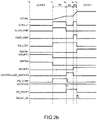
- FIG. 2b the figure 2b illustrates a timing diagram showing an example of an operating mode during a rising transition of the circuit according to the first embodiment.
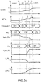
- FIG. 2c the figure 2c illustrates a block diagram showing an example of an operation mode during a rising transition of the circuit according to the first embodiment.
- FIG. 2d the 2d figure illustrates a block diagram showing an example of an operation mode during a downward transition of the circuit according to the first embodiment.
- the picture 3a illustrates an electronic circuit for selecting a supply voltage according to a second embodiment of the invention.
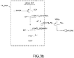
- FIG. 3b the figure 4b illustrates an exemplary embodiment of a first gradual transition circuit used in a supply voltage selection circuit according to the second embodiment of the invention.
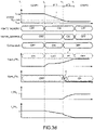
- FIG. 3c the figure 3b illustrates a timing diagram showing an example of an operating mode during a downward transition of the circuit according to the second embodiment.
- FIG. 3d the figure 3c illustrates a block diagram showing an example of an operation mode during a downward transition of the circuit according to the second embodiment.
- FIG. 3rd the 3d figure illustrates a block diagram showing an example of an operation mode during a rising transition of the circuit according to the second embodiment.
- FIG. 4a the figure 4a illustrates an embodiment of a linear voltage regulation circuit of the circuit for selecting a supply voltage according to the invention.
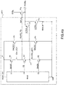
- FIG. 4b the figure 4b illustrates an embodiment of a second gradual transition circuit of the supply voltage selection circuit according to the invention.
- the figure 2a illustrates an electronic circuit for selecting a supply voltage VSj according to a first embodiment of the invention.
- the circuit for selecting a supply voltage VSj of rank j provides the calculation core COREj of the same rank j (not shown) with the supply voltage chosen according to the resource requirements of the core as explained above.
- VDDH for the high supply voltage
- VDDL for the low supply voltage.
- the characteristics of the invention remain generalizable for a plurality of supply voltage levels.
- the circuit for selecting a supply voltage VSj comprises a first node 101 adapted to receive a first input supply voltage VDDH; a second node 102 adapted to receive a second input supply voltage VDDL lower than the first input supply voltage VDDH; a third node 103 adapted to provide an output supply voltage VCORE to the associated calculation core.
- the circuit for selecting a supply voltage VSj comprises a first power transistor PSH connecting the first node 101 to the third node 103; a second power transistor PSL connecting the second node 102 to the third node 103.
- the power transistors are PMOS type transistors. It is also possible to use NMOS type transistors while adapting the control signals to this type of transistor.
- the circuit for selecting a supply voltage VSj comprises a configuration circuit CONF adapted in a first configuration, to maintain the first and second transistors PSH and PSL, respectively in an on and blocking (or blocked) state of so as to apply the first input supply voltage VDD H to the third node 103.
- the configuration circuit CONF is adapted to maintain the first and second transistors PS H and PS L respectively in the blocking and on state so as to apply the second input supply voltage VDD L to the third node 103.
- the circuit for selecting a supply voltage VS j further comprises a fourth node 104 adapted to receive a third supply voltage VMAX equal to the maximum supply voltage VDD H and used to supply the operation of a part or of the entire configuration circuit CONF.
- the source of the PMOS type transistor PS L is not connected directly to the node 102 but through an NMOS type transistor denoted SWPG2 having a resistivity, in the off state, greater than that of PS L and thus making it possible to reduce the leakage currents via the node 102.
- SWPG2 NMOS type transistor
- the source of the PMOS type transistor PS H is not connected directly to the node 101 but through an NMOS type transistor denoted SWPG1 having a higher resistivity than that of PSH and thus making it possible to reduce the leakage currents via the node 101 when VDD H is not selected.
- the configuration circuit CONF is not connected directly to the node 104 but through an NMOS type transistor denoted SWPGVMAX having a higher resistivity than the transistors of the sub-blocks of the configuration circuit CONF and thus making it possible to reduce the currents of leakage via the node 104.
- the configuration circuit CONF is thus supplied with the voltage VMAX_INT at the drain of the intermediate transistor SWPGVMAX.
- the limitation of the leakage currents in this case is obtained by placing the transistor SWPGVMAX in a blocking state via the signal EN_SWPGVMAX when the configuration circuit is deactivated.
- the current leakage limiting transistors SWPG1, SWPG2 and SWPGVMAX are transistors having a gate made with a thicker oxide layer than that of the transistors PS H and PS L so as to obtain a higher resistivity for the current leakage limiting transistors.
- the circuit for selecting a supply voltage VS j further comprises a fifth node 105 adapted to receive a fourth supply voltage VANA higher than the maximum supply voltage VDD H and used to supply the operation of part or all of the configuration circuit CONF and control the transistors for the current leakage limiting transistors.
- the configuration circuit CONF comprises the following sub-blocks: a first transition management circuit CGT H , a second transition management circuit CGT L , a comparator COMP, a circuit for generating rising or falling voltage ramps RMP, an LED delay generation circuit and an FSM asynchronous sequencing circuit implementing a previously programmed state machine.
- the first transition management circuit CGT H comprises a first linear regulation circuit LDO1 for controlling the first transistor PS H in linear mode, and having a first input node ldo1_e1 connected to the third node 103, a second input node ldo1_e5 connected to the output node s_rmp of the ramp generator RMP, and an output node ldo1_s connected to the gate of the first PS transistor H_ through a first switch i1.
- the first linear regulation circuit LDO1 forms an analog feedback loop suitable for controlling the transistor PS H in linear mode to control the output supply voltage VCORE supplied to the node 103.
- the regulation circuit LDO1 comprises an input node ldo1_e5 to receive a voltage ramp VCTRL to be transferred to the node 103.
- the circuit LDO1 is capable of adjusting the control signal applied, via its node ldo1_s, to the gate of the transistor PS H (corresponding to VGATE_PS H when switch i1 is on). This makes it possible to slave the output supply voltage VCORE to the voltage ramp VCTRL.
- the regulation circuit LDO1 further comprises an input node ldo1_e4 to receive an activation signal EN_LDO1 from the circuit LDO1. It further comprises an input node ldo1_e3 to receive a hold signal SWON1 in the closed state (on) of the transistor PS H following a rising transition, and an input node ldo1_e2 to receive a hold signal SWOFF1 to the open (blocked) state of transistor PS H following a falling transition.
- the regulation circuit LDO1 further comprises a supply node ldo1_p connected to the node for supplying the internal supply voltage VMAX INT.
- the second transition management circuit CGT L is configured to control the gate of the second transistor PS L during the rising or falling transition when the switch i3 is on so as to apply a control signal VGATE_PS L exhibiting a gradual variation.
- a gradual voltage variation is a variation over time that can be modeled according to a logarithmic law ln(x), a linear law with a slow slope ( ⁇ 1V/ ⁇ s in absolute value), or a law exp(-x) with x>0.
- the second transition management circuit CGT L comprises a gradual transition circuit noted TR_GR2 capable of carrying out the gradual control function of the transistor PS L via a switch i4.
- Switch i4 is closed when at least one of the CONTROLLED_SWOFF2 or CONTROLLED_SWON2 signals is activated.
- a logic cell carrying out the "OR" function is used.
- a resistor or a capacitive element it is possible to use a resistor or a capacitive element.
- the second transition management circuit CGT L comprises a second linear regulation circuit LDO2 for controlling the second transistor PS L in linear mode during the rising and falling transitions between VDD L and the electrical ground during standby of the core CORE j associated with the selection circuit VS j .
- the second linear regulation circuit LDO2 has a first input node ldo2_e1 connected to the third node 103, a second input node ldo2_e5 connected to the output node s_rmp of the ramp generator RMP, and an output node ldo2_s connected to the gate of the second transistor PS L_ through a controlled switch i3.
- the second linear regulation circuit LDO2 forms an analog feedback loop suitable for controlling the transistor PS L in linear mode to control the output supply voltage VCORE supplied to the node 103.
- the regulation circuit LDO2 includes an ldo2_e5 input node to receive a VCTRL voltage ramp to be reported to node 103 when activated by the EN_LDO2 signal.
- Circuit LDO2 is able to adjust the control signal applied, via its node ldo2_s, to the gate of transistor PS H (corresponding to VGATE_PS L when switch i3 is on). This makes it possible to slave the output supply voltage VCORE to the voltage ramp VCTRL.
- the regulation circuit LDO2 further comprises an input node ldo2_e4 to receive the activation signal EN_LDO2 from the circuit LDO2. It further comprises an input node ldo2_e3 to receive a hold signal SWON2 in the closed (on) state of transistor PS L following a falling transition, and an input node ldo2_e2 to receive a hold signal SWOFF2 to the open (blocked) state of transistor PS L following a rising transition.
- the regulation circuit LDO2 further comprises a supply node ldo2_p connected to the node supplying the internal supply voltage VMAX INT.
- the ramp generation circuit RMP comprises an output node s_rmp connected to the input nodes ldo1_e5 and ldo2_e5 of the linear regulation circuits LDO1 and LDO2 and supplying the voltage ramp VCTRL applied to the circuits LDO1 and LDO2.
- the circuit RMP comprises an input node e1_rmp intended to receive a control signal CTRLUP and an input node e2_rmp intended to receive a control signal CTRLDW.
- the control signal CTRLUP When the control signal CTRLUP is activated, the circuit RMP is configured to generate on its output node s_rmp a predetermined increasing voltage ramp.
- the RMP circuit When the control signal CTRLDW is activated, the RMP circuit is configured to generate on its node s_rmp a decreasing voltage ramp predetermined.
- the circuit RMP further comprises an input node e3_rmp intended to receive a command signal FAST_RMP and an input node e4_rmp intended to receive a command signal SLOW_RMP.
- the control signal SLOW_RMP When the control signal SLOW_RMP is activated, the circuit RMP is configured to generate on its output node s_rmp a voltage ramp having a first predetermined slope to obtain a slow ramp.
- the circuit RMP When the control signal FAST_RMP is activated, the circuit RMP is configured to generate on its output node s_rmp a voltage ramp having a second slope much lower in absolute value than the first slope to obtain a fast ramp.
- a slow ramp has an increasing or decreasing slope less in absolute value than 1V/ ⁇ s.
- the absolute value of the second slope is between 5 and 10 times the absolute value of the slow slope.
- the circuit RMP comprises a supply node p_rmp connected to the node for supplying the internal supply voltage VMAX_INT.
- the production of the voltage ramp generation circuit RMP has not been detailed, the embodiments described being compatible with all or most of the known voltage ramp generation circuits.
- the delay generation circuit DEL comprises an input node e1_del intended to receive an activation signal EN_DELAY, and an output node s_del.
- the circuit DEL is intended to provide, on its output node s_del, a signal DELAY_OK presenting a pulse after a predetermined delay. More particularly, the circuit DEL is intended to reproduce on its output s_del, with a predetermined delay, a change of state of the signal DELAY_OK applied to its input node e1_del.
- the LED circuit further comprises a supply node p at the node for supplying the internal supply voltage VMAX_INT.
- the voltage comparator VCMP has a first input terminal e- and a second input terminal e+.
- the first input terminal e- is connected on the one hand to the node 103 of application of the output supply voltage VCORE via a switch K4, and on the other hand to the node 102 of application of the low input supply voltage VDD L via a switch K3.
- the second input terminal e+ is connected on the one hand to the application node 103 of the output supply voltage VCORE via a switch K2, and on the other hand to the node 101 of application of the low input supply voltage VDD H via a switch K1.
- the voltage comparator VCMP comprises an output node s_cmp and it is intended to provide, on this node s_cmp, a voltage VCOVVDD changing level when the voltage applied to its input node e+ reaches a predetermined threshold depending on that of the voltage applied to its entry node e-.
- the comparator VCMP compares the output supply voltage VCORE with a first threshold V threshold1 equal to VDD L + ⁇ V with ⁇ V>0.
- the comparator VCMP compares the output supply voltage VCORE with a second threshold V threshold2 equal to VDD H - ⁇ V with ⁇ V>0.
- the voltage comparator VCMP further comprises a supply node p connected to the node for supplying the internal supply voltage VMAX_INT.
- the construction of the voltage comparison circuit VCMP has not been detailed, the embodiments described being compatible with all or most of the known voltage comparison circuits.
- the sequencing circuit FSM further comprises a control input 310 on one or more bits (DIGBUS[1:x]) making it possible to control the voltage selection circuit in the first configuration (transistor PS H and PS L respectively closed and open) or in the second configuration (transistor PS H and PS L respectively open and closed), and, if necessary, to configure certain parameters of the configuration circuit CONF.
- the sequencing circuit FSM further comprises a supply node p1_fsm connected to the node for supplying the internal supply voltage VMAX_INT.
- the sequencing circuit FSM further comprises a supply node p2_fsm connected to the supply voltage supply node VANA.
- the figure 2b illustrates a timing diagram showing an example of a mode of operation during a rising transition of the circuit according to the first embodiment of the figure 2a .
- the figure 2c illustrates a block diagram showing the mode of operation of the selection circuit VS j of the first embodiment during a rising transition.
- the references t0, t1, t2, t3 and t4 are common to the figure 2b and 2c .
- the figure 2b illustrates the sequence of some control signals of the selection circuit making it possible to obtain the operation of said circuit as illustrated in the figure 2c . We recall that this is an upward transition and therefore the system evolves from the second configuration CONF2 to the first configuration CONF1.
- selection circuit VSj is in a state corresponding to second configuration CONF2 where configuration circuit CONF maintains first and second transistors PS H and PS L respectively in blocking and on state so as to apply second input supply voltage VDD L on the third node 103.
- the CTRLUP, SLOW_RMP, FAST_RMP, EN_LDO1, CONTROLLED_SWOFF2, EN_VCMP, VCOVVDD, EN_DELAY, and DELAY_OK signals are at a low state (disabled) since the system is in a stationary at this time.
- the signals SWON1, SWOFF1 are respectively in a low (deactivated) and high (activated) state to maintain the transistor PS H in the blocking state.
- the gate voltage of the transistor PS H VGATE_PS H at a high level, the transistor PS H in the blocking state and the current I_ PS H through PS H is zero or almost zero.
- the signals SWOFF2, SWON2 are respectively in a low (deactivated) and high (activated) state to maintain the transistor PS L in the on state.
- the gate voltage of the transistor PS L VGATE_PS L at a low level, the transistor PS L in the on state and the current I_PS L through PS L is equal to I L >0.
- the first phase ⁇ 1 of the rising transition is triggered.
- the passage of the ramp generator control signals CTRUP and SLOW_RMP to a high state activates the generation of an increasing voltage ramp having a predetermined slow slope.
- the shape of the ramp on the VCTRL signal is observed.
- the hold signals SWOFF1, SWON1, SWOFF2 and SWON2 all go low.
- the activation signal of the comparator circuit EN_CMP also goes to a high state, thus turning on the comparator for ⁇ 1.
- the activation signal EN_LDO1 activates the first linear regulation circuit LDO1 so as to control the first transistor PS H in linear mode for apply the slow voltage ramp VCTRL_ on the third node 103 during the slow phase ⁇ 1 as indicated on the evolution of the output supply voltage VCORE on the figure 2c .
- This evolution of VCORE according to a slow slope ( ⁇ 1V/ ⁇ s) makes it possible to minimize the variation of the current l_PS H through PS H in the short time thus making it possible to solve the problem of switching noise generated by the proportional voltage variations d ( l_PS H )/dt at the terminals of the parasitic inductances of the supply rails.
- comparator VCMP detects the passage of the output supply voltage beyond threshold voltage V threshold2 equal to VDD H - ⁇ V with ⁇ V>0. The comparator VCMP thus generates a falling pulse via the output signal VCOVVDD. Following this detection, the next phase ⁇ 2 is triggered with the passage of the SLOW_RMP signal and of the CTRUP signal to a low state (deactivated) thus stopping the generation of the slow slope ramp on the VCTRL signal and thus the supply voltage of VCORE output via the enslavement carried out by the LDO1 circuit always activated. Thus, the VCTRL signal (and therefore VCORE) are maintained at a constant voltage as shown in the figure 2c for the predetermined time between t2 and t3.
- This predetermined duration then defines a constant intermediate phase ⁇ 2 where the transition of transistor PS H from an off state to an on state is paused.
- the signal CONTROLLED_SWOFF2 goes to a high state thus activating the gradual transition circuit TR_GR2.
- the gradual transition circuit TR_GR2 applies, during the intermediate phase ⁇ 2, a control signal VGATE_PS L having a gradual variation on the gate of the second transistor PS L to gradually switch the second transistor PS L to a blocking state as represented in the diagrams, VGATE_PS L (voltage on the gate PS L ) of l_PS L (current through PS L ) of the figure 2c .
- Switch i4 is closed throughout the intermediate phase ⁇ 2.
- the gradual and controlled closing in voltage and current of the transistor PS L thus makes it possible to solve the problem of switching noise generated by the proportional voltage variations d (l_PS L )/dt at the terminals of the parasitic inductances of the power supply rails.
- pausing the closing of transistor PS H during intermediate phase ⁇ 2 makes it possible to eliminate the possibility of having a moment during the transition where the two transistors PS L and PS H are on at the same time. This eliminates any risk of reverse current problems.
- the comparator circuit VCMP is stopped via the signal EN_VCMP to limit the overall consumption of the circuit. Additionally, the delay generation circuit is activated via the EN_DELAY signal to start counting the preset delay for the rest of the rising transition.
- transistor PS L switches completely into a blocking state as illustrated in figure figure 2c where the current l_PS L is zero or almost zero.
- the closing of transistor PS H is resumed and phase ⁇ 3 is triggered.
- the passage of the ramp generator control signals CTRUP and FAST_RMP to a high state activates the generation of an increasing voltage ramp having a predetermined rapid slope. The shape of the ramp on the VCTRL signal is observed.
- the activation signal EN_LDO1 always keeps the first linear regulation circuit LDO1 in operation so as to control the first transistor PS H in linear mode to apply the fast voltage ramp VCTRL_on the third node 103 during the fast phase ⁇ 3 as is indicated on the evolution of the output supply voltage VCORE on the figure 2c which reaches the high supply voltage value VDD H .
- the fast phase ⁇ 3 makes it possible to finalize the rising transition in a reduced time so as to always maintain a transition speed from one supply voltage to another while reducing inductive switching noise disturbances. Indeed, the starting point of the VCORE voltage at t3 is close to the target supply voltage VDD H , thus the current draw through l_PS H is reduced as illustrated in the figure 2c hence the noise reduction even with a steep slope at the end of the transition.
- the previously activated delay generation circuit generates via the DELAY_OK signal a pulse indicating that the predetermined duration provided for all of the phases ⁇ 2 and ⁇ 3 has elapsed. This corresponds to the end of the rising transition and the passage to the first configuration CONF1.
- the CTRLUP, SLOW_RMP, FAST_RMP, EN_LDO1, CONTROLLED_SWOFF2, EN_VCMP, VCOVVDD, EN_DELAY, and DELAY_OK signals are low (off) since the system is in a stationary state at this time.
- the signals SWOFF1, SWON1 are respectively at a low (deactivated) and high (activated) state to maintain the transistor PS H in the on state via the switch i1 closed.
- the gate voltage of the transistor PS H VGATE_PS H at a low level, the transistor PS H in the on state and the current l_PS H through PS H is equal to l M >0.
- the signals SWON2, SWOFF2 are respectively in a low (deactivated) and high (activated) state to maintain the transistor PS L in the blocking state through the switch i3 closed.
- the gate voltage of the transistor PS L VGATE_PS L at a high level, the transistor PS L in the blocking state and the current I_ PS L through PS L is zero or almost zero.
- the 2d figure illustrates a block diagram showing the mode of operation of the selection circuit VS j of the first embodiment during a downward transition of the voltage VCORE from the high supply voltage VDD H to the low supply voltage VDD L During the entire transition falling, switch i1 is kept closed, switches K3 and K2 are kept closed and switches K1 and K4 open so as to compare VCORE with the second threshold V threshold1 equal to VDD L + ⁇ V with ⁇ V>0.
- the selection circuit VS j is in a state corresponding to the first configuration CONF1 where the configuration circuit CONF maintains the first and second transistors PS H and PS L respectively in the on and off state so as to apply the high input supply voltage VDD H on third node 103.
- the CTRLDW, SLOW_RMP, FAST_RMP, EN_LDO1, CONTROLLED_SWOFF2, EN_VCMP, VCOVVDD, EN_DELAY, and DELAY_OK signals are low (disabled) since the system is in a stationary state at this time.
- the signals SWOFF1, SWON1 are respectively at a low (deactivated) and high (activated) state to maintain the transistor PS H in the on state via the switch i1 closed.
- the gate voltage of the transistor PS H VGATE_PS H at a low level, the transistor PS H in the on state and the current l_PS H through PS H is equal to l M >0.
- the signals SWON2, SWOFF2 are respectively at a low (deactivated) and high (activated) state to maintain the transistor PS L in the blocking state via the switch i3 closed.
- the gate voltage of the transistor PS L VGATE_PS L is at a high level, the transistor PS L is in the blocking state and the current I_PS L through PS L is zero or almost zero.
- the first phase ⁇ '1 of the falling transition is triggered.
- the transition of the ramp generator control signals CTRDW and FAST_RMP to a high state activates the generation of a voltage ramp descending with a pre-determined steep slope.
- the shape of the ramp on the VCTRL signal is observed.
- the hold signals SWOFF1, SWON1, SWOFF2 and SWON2 all go low.
- the activation signal of the comparator circuit EN_CMP also goes to a high state, thus putting the comparator in operation for ⁇ ′1.
- the activation signal EN_LDO1 activates the first linear regulation circuit LDO1 so as to control the first transistor PS H in linear mode to apply the fast voltage ramp VCTRL_on the third node 103 during the fast phase ⁇ '1 as c' is indicated on the evolution of the output supply voltage VCORE on the 2d figure .
- comparator VCMP detects the passage of the output supply voltage to a value lower than threshold voltage V threshold1 equal to VDD L + ⁇ V with ⁇ V>0. The comparator VCMP thus generates a pulse via the output signal VCOVVDD. Following this detection, the next phase ⁇ '2 is triggered with the passage of the FAST_RMP signal to a low state (deactivated) and the passage of the SLOW_RMP signal to a high state, thus allowing the generation of the slow slope ramp on the VCTRL signal and thus on the output supply voltage VCORE via the enslavement performed by the circuit LDO1 which is always activated.
- the VCTRL signal (and therefore VCORE) follows a slow decreasing ramp as shown in the 2d figure for the predetermined time between t2 and t3.
- the signal CONTROLLED_SWON2 goes to a high state thus activating the gradual transition circuit TR_GR2.
- the gradual transition circuit TR_GR2 applies, during the intermediate phase ⁇ '2, a control signal VGATE_PS L having a gradual decreasing variation on the gate of the second transistor PS L to gradually switch the second transistor PS L to an on state such as represented in the diagrams, VGATE_PS L (voltage on the gate PS L ) of l_PS L (current through PS L ) of the 2d figure .
- the switch i4 is closed throughout the slow phase ⁇ '2.
- the gradual and controlled closing in voltage and current of the transistor PS L thus makes it possible to solve the problem of switching noise generated by the proportional voltage variations d (l_PS L )/dt at the terminals of the parasitic inductances of the power supply rails.
- the delayed triggering of the closing of the transistor PS L during the intermediate phase ⁇ '2 makes it possible to eliminate the possibility of having a moment during the transition where the two transistors PS L and PS H are fully on at the same time. This eliminates any risk of reverse current problems.
- the comparator circuit VCMP is stopped via the signal EN_VCMP to limit the overall consumption of the circuit.
- the delay generation circuit is activated via the EN_DELAY signal to start counting the predefined delay for the slow phase ⁇ '2.
- the previously activated delay generation circuit generates via the DELAY_OK signal a pulse indicating that the predetermined duration provided for the phase ⁇ ′2 has elapsed. This corresponds to the end of the downward transition and the passage to the second configuration CONF2.
- the CTRLUP, SLOW_RMP, FAST_RMP, EN_LDO1, CONTROLLED_SWOFF2, EN_VCMP, VCOVVDD, EN_DELAY, and DELAY_OK signals are low (off) since the system is in a stationary state at this time.
- the signals SWON1, SWOFF1 are respectively in a low (deactivated) and high (activated) state to maintain the transistor PS H in the blocking state via the switch i1 closed.
- the gate voltage of the transistor PS H VGATE_PS H at a high level, the transistor PS H in the blocking state and the current I_PS H through PS H is zero or almost zero.
- the signals SWON2, SWOFF2 are respectively in a high (activated) and low (deactivated) state to maintain the transistor PS L in the on state with the switch i3 closed.
- the gate voltage of the transistor PS L VGATE_PS L at a low level, the transistor PS L in the on state and the current l_ PS L through PS L is equal to l L >0.
- the picture 3a illustrates an electronic circuit for selecting a supply voltage according to a second embodiment of the invention.
- the selection circuit VS j uses the same elements previously described for the first embodiment with a difference consisting of the following.
- the first transition management circuit CGT H further comprises a gradual transition circuit TR_GR1 having an output node gr1_s connected to the gate of the first transistor PS H through a switch i2.
- the first gradual transition circuit TR_GR1 is capable of applying a control signal VGATE_PS H exhibiting a gradual variation on the gate of the second transistor PS L when the second switch i2 is on.
- the switch i2 is closed when the VGATE_MEMORY signal is activated.
- the gradual transition circuit TR_GR1 receives two activation signals VGATE_MEMORY and VGATE_CONTROL.
- a gradual voltage variation is a variation over time that can be modeled according to a logarithmic law ln(x), a linear law with a slow slope ( ⁇ 1V/ ⁇ s in absolute value), or a law exp(-x) with x>0.
- the gradual transition is obtained for example via the charging and discharging of a capacitive element having a terminal connected to the gate VGATE_PS H .
- the figure 3b illustrates an example of implementation of the gradual transition circuit TR_GR1 according to the invention.
- the gradual transition circuit TR_GR1 comprises a PMOS-type transistor SC1 controlled by a bias signal BIASP, a switch ic1 controlled by the signal VGATE_CONTROL, a switch ic2 controlled by the signal VGATE_MEMORY, and a capacitive element C1.
- the source of the transistor SC1 is connected to the internal supply voltage, the drain is connected, when the switch ic1 is on, to the output node gr1_s corresponding to the control signal VGATE_PS H and the gate is biased so as to produce a Power source.
- the switch ic1 is conducting when VGATE_CONTROL is activated and blocking in the opposite case.
- the ic2 switch is on when VGATE_MEMORY is activated and off in the opposite case.
- the capacitive element C1 is connected on the one hand to the electrical ground and on the other hand to the output node gr1_s corresponding to the control signal VGATE_PS H when the switch i2 is on.
- the capacitive element acts as a memory point local of the VGATE_PS H signal collected on the output node gr1_s.
- FIG. 3c illustrates a timing diagram showing an example of a mode of operation during a downward transition of the circuit according to the second embodiment of the picture 3a .
- the 3d figure illustrates a block diagram showing the mode of operation of the selection circuit VS j of the second embodiment during a downward transition.
- the references t0, t1, t2 and t3 are common to the figure 3c and 3d .
- the figure 3c illustrates the sequence of some control signals of the selection circuit making it possible to obtain the operation of said circuit as illustrated in the 3d figure .
- This is a downward transition and therefore the system evolves from the first configuration CONF1 to the second configuration CONF2.
- the selection circuit VSj is in a state corresponding to the first configuration CONF1 where the configuration circuit CONF maintains the first and second transistors PSH and PSL respectively in the on and off state so as to apply the voltage of high input supply VDDH on the third node 103.
- the signals CTRLDW, SLOW_RMP, FAST_RMP, EN_LDO1, CONTROLLED_SWOFF2, EN_VCMP, VCOVVDD,VGATE_MEMORY and VGATE_CONTROL are low (disabled) since the system is in a stationary state at this time.
- the signals SWOFF1, SWON1 are respectively at a low (deactivated) and high (activated) state to maintain the transistor PSH in the on state via the switch i1 closed.
- the gate voltage of the PSH transistor VGATE_PSH at a low level, the PSH transistor in the on state and the current l_PSH through PSH is equal to lM >0.
- the signals SWON2, SWOFF2 are respectively at a low (deactivated) and high (activated) state to maintain the transistor PSL in the blocking state via the switch i3 closed.
- the gate voltage of the PSL transistor VGATE_PSL is at a high level, the PSL transistor is in the blocking state and the current I_PSL through PSL is zero or almost zero.
- the first phase ⁇ ′′′1 of the falling transition is triggered.
- the passage of the ramp generator control signals CTRDW and FAST_RMP to a high state activates the generation of a decreasing voltage ramp having a predetermined rapid slope.
- the shape of the ramp on the VCTRL signal is observed.
- the hold signals SWOFF1, SWON1, SWOFF2 and SWON2 all go low.
- the activation signal of the comparator circuit EN_CMP also goes to a high state, thus putting the comparator on for ⁇ ′′′1.
- the activation signal EN_LDO1 activates the first linear regulation circuit LDO1 so as to control the first transistor PS H in linear mode to apply the fast voltage ramp VCTRL_on the third node 103 during the fast phase ⁇ ′′′1 as is indicated on the evolution of the output supply voltage VCORE on the figure 3c .
- the VGATE_MEMORY signal is activated to record an image of the evolution of the VGATE_PS H signal in the memory point to be produced by the capacitor C1 of the gradual transition circuit TR_GR1.
- comparator VCMP detects the passage of the output supply voltage to a value lower than threshold voltage V threshold1 equal to VDD L + ⁇ V with ⁇ V>0. The comparator VCMP thus generates a pulse via the output signal VCOVVDD. Following this detection, the next phase ⁇ '"2 is triggered with the transition of the EN_LDO1 and FAST_RMP signals to a low state (disabled) and the VGATE_CONTROLLED signal going high. As explained previously, the simultaneous activation of VGATE_CONTROLLED and VGATE_MEMORY thus makes it possible to apply a control signal VGATE_PS H exhibiting a gradual increasing variation on the gate of the first transistor PS H .
- the signal CONTROLLED_SWON2 goes to a high state thus activating the gradual transition circuit TR_GR2.
- the gradual transition circuit TR_GR2 applies, during the intermediate phase ⁇ ′′′2, a control signal VGATE_PS L having a gradual decreasing variation on the gate of the second transistor PS L to gradually switch the second transistor PS L to an on state as represented in the diagrams, VGATE_PS L (voltage on the gate PS L ) of l_PS L (current through PS L ) of the 3d figure .
- the switch i4 is closed throughout the slow phase ⁇ '"2.
- the gradual and controlled closing in voltage and current of the transistors PS L and PS H thus makes it possible to solve the problem of switching noise generated by the proportional voltage variations d (l_PS L )/dt and d ( l_PS H )/dt at the terminals of the parasitic inductances of the supply rails. the possibility of having a moment during the transition where the two transistors PS L and PS H are fully on at the same time. This eliminates any risk of reverse current problems.
- the comparator circuit VCMP is stopped via the signal EN_VCMP to limit the overall consumption of the circuit.
- the delay generation circuit is activated via the EN_DELAY signal to start counting the preset delay for the slow phase ⁇ ′′′2.
- the previously activated delay generation circuit generates via the DELAY_OK signal (not shown) a pulse indicating that the predetermined duration provided for the phase ⁇ '"2 has elapsed. This corresponds to the end of the downward transition and the passage to the second configuration CONF2
- the CTRLDW, SLOW_RMP, FAST_RMP, EN_LDO1, CONTROLLED_SWOFF2, EN_VCMP, VCOVVDD,VGATE_MEMORY and VGATE_CONTROL signals are in a low state (deactivated) since the system is in a stationary state at this instant. , SWOFF1 are low (disabled) and high respectively (activated) to keep transistor PS H in the blocking state via switch i1 closed.
- the gate voltage of the transistor PS H VGATE_PS H at a high level, the transistor PS H in the blocking state and the current I_ PS H through PS H is zero or almost zero.
- the signals SWON2, SWOFF2 are respectively in a high (activated) and low (deactivated) state to maintain the transistor PS L in the on state with the switch i3 closed.
- the gate voltage of the transistor PS L VGATE_PS L at a low level, the transistor PS L in the on state and the current l_PS L through PS L is equal to l L >0.
- the figure 3e illustrates a timing diagram showing an example of a mode of operation during a rising transition of the circuit according to the second embodiment of the picture 3a .
- the operation of the first transistor PS H is presented, which changes with respect to the rising transition of the first embodiment.
- the control of the signal VGATE_PS H is not carried out via the activation of the first linear regulation circuit LDO1 which receives a ramp but by directly applying a control signal VGATE_PS H exhibiting a gradual decreasing variation on the gate of the first transistor PS H using the gradual transition circuit TR_GR1.
- the figure 4a illustrates an embodiment of the first linear voltage regulation circuit LDO1 implemented as a supply voltage selection circuit according to the invention.
- the LDO1 linear voltage regulation circuit of the figure 4a includes a BIAS bias circuit powered by the voltage VMAX_INT.
- the bias circuit BIAS comprises a node s1 for supplying a bias voltage BIASP, a node s2 for supplying a bias voltage VB, and a node s3 for supplying a bias voltage BIASN.
- Circuit LDO1 further comprises a PMOS-type transistor P1 connecting, via its conduction nodes, the voltage supply node VMAX_INT to the output node of LDO1 denoted ldo1_s, and therefore the gate of transistor PS H .
- the gate of transistor P1 is connected to output node s1 of the BIAS circuit to receive the bias signal BIASP.
- Circuit LDO1 further comprises a transistor N1 of NMOS type connecting, via its conduction nodes, the output node ldo1_s of the circuit LDO1 to an intermediate node n1, and an N-type transistor N2 connecting, via its conduction nodes, the node n1 to ground VSS.
- the gate of transistor N1 is connected to output node s2 of the BIAS circuit to receive the bias signal VB, and the gate of transistor N2 is connected to output node s3 of the BIAS circuit to receive the bias signal BIASN.
- the LDO1 circuit of the figure 4a further comprises a PMOS-type transistor P3 connecting, via its conduction nodes, the supply node of the voltage VCORE, to the internal node n1.
- the gate of transistor P3 is connected to the ramp voltage supply node VCTRL.
- the circuit LDO1 further comprises a PMOS-type transistor P4 connected in series, via its conduction nodes, with a resistor RDISLIM, between the ramp voltage supply node VCTRL and the electrical ground VSS.
- the gate of transistor P4 is connected to the node for applying the setpoint voltage VCTRL.
- the LDO1 circuit of the figure 4a further comprises a PMOS type transistor P2 connecting, via its conduction nodes, the supply node p of the circuit LDO1 to its output node ldo1_s, and an NMOS type transistor N3 connecting, via its conduction nodes, the output node ldo1_s to electrical ground VSS.
- the gate of transistor N3 is connected to the application node of control signal SWON1, and the gate of transistor P2 is by the logical inverse of control signal SWOFF1.
- the logical inverse is obtained by means of an inverter, not shown, to simplify the presentation.
- the figure 4b illustrates an embodiment of the gradual transition circuit TR_GR2 of the circuit for selecting a supply voltage according to the invention.
- resistors can be used to generate step-change control signals.
- the gradual transition circuit TR_GR2 comprises a controlled PMOS type transistor P5 by a BIASP bias signal, a PMOS-type transistor N4 controlled by a BIASN bias signal, a switch ic3 controlled by the logical inverse of the signal CONTROLLED_SWOFF2, a switch ic4 controlled by the signal SWON2, a switch ic5 controlled by the signal CONTROLLED_SWON2 and a capacitive element C2.
- the BIASP and BIASN bias signals are generated by a common BIAS bias circuit with other blocks and not shown for the sake of simplification.
- the source of transistor P5 is connected to the internal supply voltage VMAX_INT when switch ic3 is on and its drain is connected to the output node corresponding to the gate of PS L
- the gate of P5 is biased so as to produce a source current.
- the source of transistor N4 is connected to ground VSS when switch ic5 is on and its drain is connected to the output node connected to the gate of PS L.
- the gate of N4 is biased so as to produce a current source.
- Switch ic3 is on when CONTROLLED_SWOFF2 is activated and off in the opposite case.
- Switch ic4 is on when SWON2 is activated and off in the opposite case.
- the capacitive element C2 is connected on the one hand to the electrical ground and on the other hand to the output node gr2_s corresponding to the control signal VGATE_PS L when the switch i4 is on.
- the signal CONTROLLED_SWOFF2 is activated and the other signals SWON2, CONTROLEED_SWON2 are deactivated so as to progressively charge the capacitive element C2 thus obtaining the desired gradual variation on VGATE_PS L .
- the signal CONTROLLED_SWOFF2 is deactivated and the signal CONTROLEED_SWON2 is activated so as to progressively discharge the capacitive element C2 through the branch of N4 thus obtaining the desired gradual variation on VGATE_PS L .
Landscapes
- Engineering & Computer Science (AREA)
- Physics & Mathematics (AREA)
- General Physics & Mathematics (AREA)
- Automation & Control Theory (AREA)
- Radar, Positioning & Navigation (AREA)
- Electromagnetism (AREA)
- Theoretical Computer Science (AREA)
- General Engineering & Computer Science (AREA)
- Computing Systems (AREA)
- Power Engineering (AREA)
- Mathematical Physics (AREA)
- Computer Hardware Design (AREA)
- Electronic Switches (AREA)
- Power Conversion In General (AREA)
- Logic Circuits (AREA)
Abstract
Description
- La présente invention concerne le domaine des circuits électroniques à plusieurs tensions d'alimentation et plus particulièrement un circuit de sélection de tension d'alimentation pour un circuit intégré multi-cœur.
- Dans certains dispositifs électroniques, on souhaite pouvoir modifier le niveau de la tension d'alimentation d'un circuit intégré, par exemple pour optimiser la gestion de l'énergie électrique dans le dispositif. De préférence, cette modification du niveau de la tension d'alimentation doit pouvoir se faire de façon dynamique, sans interrompre le fonctionnement du circuit intégré.
- Plus particulièrement, la gestion dynamique du niveau de la tension d'alimentation est indispensable dans le cas des circuits de calcul à haute performance HPC (acronyme de l'expression High Performance Computing). Les nouvelles architectures de processeurs de calcul haute performance sont généralement divisées en plusieurs noyaux. On parle dans cas de processeurs multi-cœurs.
- La
figure 1a illustre un schéma d'un exemple de circuit électronique comprenant une pluralité de noyaux avec une gestion de tension d'alimentation. L'exemple comprend trois sources de tensions d'alimentation à titre illustratif et non limitatif. - Le circuit électronique illustré est un processeur multicoeur PROC comprenant une pluralité de sources de tensions d'alimentation VDDH VDDM et VDDL tel que VDDH<VDDM<VDDL ; N noyaux de calcul CORE¡ et M circuits sélecteurs de tension d'alimentation VSi, avec N un entier naturel supérieur à 1 et i un entier naturel de 1 à N et avec M un entier naturel supérieur à 1 et j un entier naturel de 1 à M. Chaque circuit sélecteur de tension VSj est configuré pour fournir à au moins un noyau de calcul COREi, une tension d'alimentation choisie parmi VDDH VDDM VDDL. .
Les noyaux COREi fonctionnent à des fréquences différentes. Les charges de travail à la sortie de chaque noyau CORE¡ changent de manière dynamique lors de la réalisation des calculs. Pour chaque noyau CORE¡ la tension d'alimentation détermine la puissance de calcul et le coût énergétique des opérations logiques. En effet, un noyau de calcul fonctionnant en plein régime de calcul doit être alimenté par la tension maximale VDDH ; un noyau de calcul fonctionnant lors d'une activité de calcul moyenne peut être alimenté par la tension moyenne VDDM ; et un noyau de calcul mis en veille requiert seulement la tension minimale VDDL . Ainsi, la quantité d'opérations de calcul à réaliser et le processus algorithmique utilisé par chaque noyau CORE¡ déterminent les moyens de calcul requis et ainsi la tension d'alimentation requise pour ledit noyau en temps réel. Lors d'un changement d'activité d'un noyau COREi, la tension d'alimentation dudit noyau doit être ajustée pour minimiser le produit temps de calcul par consommation énergétique, cette technique est appelée ajustement dynamique de la tension (en anglais dynamic voltage scaling). Il est particulièrement intéressant de ne pas interrompre l'activité du cœur pendant les transitions entre deux niveaux d'alimentation. Les circuits sélecteurs de tension VSj permettent d'implémenter une gestion dynamique de la tension d'alimentation pour un grand nombre N de noyaux COREi (N>10). - Dans l'architecture présentée, les N noyaux de calcul CORE¡ et M circuits sélecteurs de tension d'alimentation VSj sont implémentés sur la même puce IC et les sources de tensions d'alimentation VDDH VDDM et VDDL sont externes à la puce IC. Les tensions d'alimentation VDDH VDDM et VDDL sont respectivement propagées vers la puce IC via les rails d'alimentations communs RH, RM et RL . Les rails d'alimentation communs étant réalisés via des matériaux conducteurs présentent toujours des effets inductifs parasites (ou d'auto-induction) présentés ici par les inductances parasites LH, LM et LL. Lors d'une transition d'une tension d'alimentation à une autre, les inductances parasites liées aux sources des tensions d'alimentation voient une forte variation de courant dans une brève période de temps ce qui génère une variation de tension aux bornes de l'inductance et donc sur les rails d'alimentation. On parle ici de « bruit de commutation » en L.di/dt. Ce type de bruit perturbe pendant les transitions les niveaux de tension d'alimentation des différents noyaux de calcul CORE¡ et donc perturber le fonctionnement de l'ensemble du circuit électronique PROC. II y a donc un effet inductif non négligeable couplant électriquement les cœurs qui sont connectés sur le même rail commun. Pendant les transitions, la variation quasi-instantanée du courant sur les rails communs, se traduit par une variation de tension sur les rails communs. Cette perturbation va se répercuter sur l'ensemble des cœurs alimentés par ceux-ci et donc modifier le fonctionnement de ces cœurs.
- La perturbation de l'alimentation subie par un noyau de calcul génère des erreurs de calcul. En effet, la fréquence de travail d'un noyau a été conçue pour être compatible avec une valeur de tension d'alimentation à priori fixe. Les perturbations à cause du phénomène d'auto-induction vont ainsi créer un incompatibilité entre la tension d'alimentation et la fréquence de travail du noyau de calcul.
- La
figure 1b illustre le problème de bruit de commutation à cause des inductances intrinsèques parasites lors d'un ou plusieurs changements de tension d'alimentation dans un circuit multicoeur avec ajustement dynamique de la tension. Le chronogramme 1c.1 illustre la variation temporelle de la tension VCORE1 qui alimente le noyau de calcul CORE1 choisie par le circuit de sélection de tension VS1. Le chronogramme 1c.2 illustre la variation temporelle de la tension VCORE2 qui alimente le noyau de calcul CORE2 choisie par le circuit de sélection de tension VS2., Le chronogramme 1c.3 illustre, plus généralement, la variation temporelle de la tension VCOREn qui alimente un noyau de calcul quelconque COREn choisi par le circuit de sélection de tension associé VSn. - A t1, la tension VCORE1 est configurée pour rester constante au niveau de tension moyen VDDM , la tension VCORE2 est configurée pour faire une transition descendante du niveau de tension haut VDDH vers le niveau de tension moyen VDDM , la tension VCOREN est configurée pour faire une transition montante du niveau de tension bas VDDL vers le niveau de tension moyen VDDM. Les commutations brusques et simultanées provoquent des appels de courant forts dans les inductances parasites LM, LL et LH dans un intervalle de temps réduit. Ainsi, les transitions réalisées pour changer l'alimentation du noyau CORE2 et du noyau COREN perturbent le rail commun RM du niveau de tension d'alimentation moyen VDDM. Cette perturbation est observable sur tous les nœuds d'alimentation VCORE1 VCORE2 jusqu'à VCOREN. A titre d'exemple, on observe une perturbation sous forme chute de tension (power drop en Anglais) sur le nœud d'alimentation VCORE1 qui est normalement configuré pour rester constante au niveau de tension moyen VDDM. Ainsi, l'élimination de la perturbation de la transition du niveau d'alimentation d'un noyau sur ceux des autres noyaux par couplage inductif des rails communs, nécessite que les transitions entre deux niveaux d'alimentation soient contrôlées en tension, mais aussi en courant. On considère qu'une tension d'alimentation est « non perturbée » lorsque les variations de cette tension sont inférieures à 5% du niveau de tension visé.
- D'autre part, il n'est pas envisageable de se contenter de ralentir la pente de transition lors de la commutation d'un niveau d'alimentation à un autre niveau pour limiter le bruit de commutation. En effet, cette approche présente un autre risque pour le circuit consistant en l'apparition de courants inverses dans les rails communs d'alimentation, ce qui perturbe le bon fonctionnement du circuit électronique PROC.
- Pour résumer, nous avons démontré que: d'une part, les variations brusques de courant dans les rails d'alimentation lors d'une transition d'un niveau de tension d'alimentation à un autre génèrent des bruits de commutation dû à l'effet inductif parasite. D'autre part, le phénomène de courant inverse présente une contrainte technique qui limite le recours au ralentissement de la pente de transition.
- Le problème technique à résoudre est alors de développer des circuits de sélection de tension d'alimentation permettant l'ajustement dynamique de la tension tout en limitant le bruit de commutation dû à l'effet inductif parasite des rails communs d'alimentation et en évitant le phénomène de courants inverses dans lesdits rails communs.
- Le brevet européen
EP3267583B1 propose une architecture de circuit de sélection de tension d'alimentation permettant de contrôler la forme de la tension sur le rail d'alimentation d'un circuit cœur de calcul pendant la transition d'un niveau de tension d'alimentation à un autre niveau . L'inconvénient de la solution proposée par le brevet précité consiste en ce qu'elle se limite à un contrôle en tension et ne tient pas en compte des forts appels de courants sur chaque rail commun. Les variations de courant ne sont pas contrôlées et le problème de bruit de commutation résultant des inductances parasites n'est pas résolu. - Le brevet américain
US10439602B2 - Le brevet américain
US10432184B1 - La demande de brevet européen
EP3734398A1 propose une architecture de circuit de sélection de tension d'alimentation utilisant un seul rail d'alimentation en entrée permettant d'assurer simultanément une tension principale et une tension configurable. L'inconvénient de la solution proposée par le brevet précité consiste en ce qu'elle nécessite un fonctionnement permanent d'un comparateur ce qui fait augmenter considérablement la consommation énergétique du circuit de sélection tension d'alimentation. De plus, la solution de la demande de brevet ne tient pas en compte des forts appels de courants sur chaque rail commun. Les variations de courant ne sont pas contrôlées et le problème de bruit de commutation à cause des inductances parasites n'est pas résolu. - Pour pallier les limitations des solutions existantes en ce qui concerne permettant l'ajustement dynamique de la tension tout en limitant le bruit de commutation inductif d'alimentation et en évitant le phénomène de courants inverses, l'invention propose différents modes de réalisation d'une architecture de circuit de sélection permettant de réaliser des transitions montante et/ou descendante selon des jeux de séquencement de phases lentes et rapides de manière à résoudre en même temps les problèmes de bruits inductifs de commutation et les problèmes de courants dans les rails d'alimentations. Cette solution présente plusieurs avantages liés à la facilité d'implémentation et la flexibilité de configurations possibles pour d'adapter aux contraintes spécifiques lors de la conception du circuit.
- L'invention a pour objet un circuit de sélection d'une tension d'alimentation, comprenant :
- un premier nœud adapté à recevoir une première tension d'alimentation d'entrée;
- un deuxième nœud adapté à recevoir une seconde tension d'alimentation d'entrée inférieure à la première tension d'alimentation d'entrée ;
- un troisième nœud adapté à fournir une tension d'alimentation de sortie;
- un premier transistor de puissance reliant le premier nœud au troisième nœud ;
- un second transistor de puissance reliant le deuxième nœud au troisième nœud ;
- et un circuit de configuration adapté dans une première configuration, à maintenir les premier et deuxième transistors respectivement passant et bloquant de façon à appliquer la première tension d'alimentation d'entrée sur le troisième nœud, et, dans une seconde configuration, à maintenir les premier et deuxième transistors respectivement en état bloquant et passant de façon à appliquer la seconde tension d'alimentation d'entrée sur le troisième nœud;
- une phase de transition de la première configuration à la seconde configuration étant dénommée transition descendante ;
- une phase de transition de la seconde configuration à la première configuration étant dénommée transition montante ;
- le circuit de configuration comprenant :
- un premier circuit de gestion de transition configuré pour commander la grille du premier transistor lors de la transition montante ou descendante de manière à appliquer sur le troisième nœud :
- ∘ au moins une première rampe de tension ayant une première pente pendant une première durée définissant une phase lente;
- ∘ et une seconde rampe de tension ayant une seconde pente étant supérieure à la première pente pendant une deuxième durée définissant une phase rapide,
- un second circuit de gestion de transition configuré pour commander la grille du second transistor lors de la transition montante ou descendante de manière à appliquer un signal de commande présentant une variation graduelle.
- un premier circuit de gestion de transition configuré pour commander la grille du premier transistor lors de la transition montante ou descendante de manière à appliquer sur le troisième nœud :
- Selon un aspect particulier de l'invention, la valeur absolue de la première pente est comprise entre un dixième de la valeur absolue de la deuxième pente et un cinquième de la valeur absolu deuxième pente.
- Selon un aspect particulier de l'invention, le circuit de configuration, pour réaliser une transition montante, est configuré pour exécuter successivement les étapes suivantes :
- i- commander le premier transistor en régime linéaire pour appliquer la première rampe de tension_sur le troisième nœud durant la phase lente;
- ii- détecter le passage de la tension d'alimentation de sortie à un niveau supérieur à un seuil prédéterminé inférieur à la première tension d'alimentation d'entrée, ledit passage indiquant l'achèvement de la phase lente ;
- iii- commander le premier transistor en régime linéaire pour appliquer une tension constante sur le troisième nœud pendant une phase intermédiaire entre la phase lente et la phase rapide;
- iv- et appliquer, pendant la phase intermédiaire, un signal de commande présentant une variation graduelle sur la grille du second transistor pour basculer graduellement le second transistor à un état bloquant ;
- v- commander le premier transistor en régime linéaire pour appliquer la seconde rampe de tension_sur le troisième nœud durant la phase rapide jusqu'au passage du premier transistor à un état passant.
- Selon un aspect particulier de l'invention, le circuit de configuration, pour réaliser une transition descendante, est configuré pour exécuter successivement les étapes suivantes :
- i- commander le premier transistor en régime linéaire pour appliquer la seconde rampe de tension_sur le troisième nœud durant la phase rapide;
- ii- détecter le passage de la tension d'alimentation de sortie à un niveau supérieur à un niveau inférieur à un seuil prédéterminé supérieur la seconde tension d'alimentation d'entrée, ledit passage indiquant l'achèvement de la phase rapide;
- iii- appliquer, pendant la phase lente, un signal de commande présentant une variation graduelle sur la grille du second transistor pour basculer graduellement le second transistor à un état passant;
- iv- et commander le premier transistor en régime linéaire pour appliquer la première rampe de tension_sur le troisième nœud durant la phase lente jusqu'au passage du premier transistor à un état bloquant.
- Selon un aspect particulier de l'invention, le circuit de configuration, pour réaliser une transition montante, est configuré pour exécuter successivement les étapes suivantes:
- i- appliquer un second signal de commande présentant une variation graduelle sur la grille du premier transistor durant la phase lente;
- ii- détecter le passage de la tension d'alimentation de sortie à un niveau supérieur à un seuil prédéterminé inférieur à la première tension d'alimentation d'entrée, ledit passage indiquant l'achèvement de la phase lente ;
- iii- commander le premier transistor en régime linéaire pour appliquer une tension constante_sur le troisième nœud pendant une phase intermédiaire_entre la phase lente et la phase rapide;
- iv- et appliquer, pendant la phase intermédiaire, un signal de commande présentant une variation graduelle sur la grille du second transistor pour basculer graduellement le second transistor à un état bloquant ;
- v- commander le premier transistor en régime linéaire pour appliquer la seconde rampe de tension_sur le troisième nœud durant la phase rapide jusqu'au passage du premier transistor à un état passant.
- Selon un aspect particulier de l'invention, le circuit de configuration, pour réaliser une transition descendante, est configuré pour exécuter successivement les étapes suivantes:
- i- commander le premier transistor en régime linéaire pour appliquer la seconde rampe de tension_sur le troisième nœud durant la phase rapide;
- ii- détecter le passage de la tension d'alimentation de sortie à un niveau supérieur à un niveau inférieur à un seuil prédéterminé supérieur la seconde tension d'alimentation d'entrée, ledit passage indiquant l'achèvement de la phase rapide;
- iii- appliquer, pendant la phase lente, un premier signal de commande présentant une variation graduelle sur la grille du second transistor pour basculer graduellement le second transistor à un état passant ;
- iv- et appliquer un second signal de commande présentant une variation graduelle sur la grille du premier transistor de manière à appliquer la première rampe de tension_sur le troisième nœud durant la phase lente; pour basculer graduellement le premier transistor à un état bloquant.
- Selon un aspect particulier de l'invention, le circuit de contrôle comprend :
- un générateur de rampes de tension pour générer :
- ∘ la première rampe de tension montante ou descendante,
- ∘ et/ou la deuxième rampe de tension montante ou descendante sur un nœud de sortie.
- et dans lequel le premier circuit de gestion de transition comprend un premier circuit de régulation linéaire pour commander le premier transistor en régime linéaire, et ayant :
- ∘ un premier nœud d'entrée connecté au troisième nœud,
- ∘ un deuxième nœud d'entrée connecté au nœud de sortie du générateur de rampes,
- ∘ et un nœud de sortie connecté à la grille du premier transistor à travers un premier interrupteur.
- Selon un aspect particulier de l'invention, le premier circuit de régulation linéaire est configuré pour commander le premier transistor en régime linéaire via l'asservissement de la tension d'alimentation de sortie sur la rampe de tension appliquée au deuxième nœud d'entrée lorsque le premier interrupteur est passant.
- Selon un aspect particulier de l'invention, le premier circuit de gestion de transition comprend en outre un premier circuit de transition graduelle ayant un nœud de sortie connecté à la grille du premier transistor à travers un deuxième interrupteur, le premier circuit de transition graduelle étant apte appliquer un signal de commande présentant une variation graduelle sur la grille du second transistor lorsque le deuxième interrupteur est passant.
- Selon un aspect particulier de l'invention, le circuit de configuration comprend en outre un second circuit de gestion de transition comprenant :
- un second circuit de régulation linéaire ayant :
- ∘ un premier nœud d'entrée connecté au troisième nœud,
- ∘ un deuxième nœud d'entrée connecté au nœud de sortie du générateur de rampes,
- ∘ et un nœud de sortie connecté à la grille du second transistor à travers un troisième interrupteur.
- Selon un aspect particulier de l'invention, le second circuit de gestion de transition comprend un second circuit de transition graduelle ayant un nœud de sortie connecté à la grille du second transistor à travers un quatrième interrupteur, ledit circuit de transition graduelle étant apte appliquer un signal de commande sur la grille du second transistor lorsque le troisième interrupteur est passant ; ledit signal de commande présentant une variation croissante ou décroissante graduelle.
- Selon un aspect particulier de l'invention, le circuit de configuration comprend en outre un circuit de comparaison de la tension d'alimentation de sortie à un seuil prédéterminé.
- Selon un aspect particulier de l'invention, le circuit de configuration comprend en outre un circuit de génération d'une durée prédéterminé.
- D'autres caractéristiques et avantages de la présente invention apparaîtront mieux à la lecture de la description qui suit en relation aux dessins annexés suivants.
- [
Fig. 1a ] lafigure 1a illustre un schéma d'un exemple de circuit électronique comprenant une pluralité de noyaux avec une gestion de tension d'alimentation. - [
Fig. 1b ] lafigure 1b illustre le bruit de commutation à cause des inductances intrinsèques dans l'exemple de circuit électronique de lafigure 1a . - [
Fig. 2a ] lafigure 2a illustre un circuit électronique de sélection d'une tension d'alimentation selon un premier mode de réalisation de l'invention. - [
Fig. 2b ] lafigure 2b illustre un chronogramme présentant un exemple d'un mode de fonctionnement pendant une transition montante du circuit selon le premier mode de réalisation. - [
Fig. 2c ] lafigure 2c illustre un schéma fonctionnel présentant un exemple d'un mode de fonctionnement pendant une transition montante du circuit selon le premier mode de réalisation. - [
Fig. 2d ] lafigure 2d illustre un schéma fonctionnel présentant un exemple d'un mode de fonctionnement pendant une transition descendante du circuit selon le premier mode de réalisation. - [
Fig. 3a ] lafigure 3a illustre un circuit électronique de sélection d'une tension d'alimentation selon un second mode de réalisation de l'invention. - [
Fig. 3b ] lafigure 4b illustre un exemple de réalisation d'un premier circuit de transition graduelle utilisé dans circuit de sélection d'une tension d'alimentation selon le second mode de réalisation de l'invention. - [
Fig. 3c ] lafigure 3b illustre un chronogramme présentant un exemple d'un mode de fonctionnement pendant une transition descendante du circuit selon le second mode de réalisation. - [
Fig. 3d ] lafigure 3c illustre un schéma fonctionnel présentant un exemple d'un mode de fonctionnement pendant une transition descendante du circuit selon le second mode de réalisation. - [
Fig. 3e ] lafigure 3d illustre un schéma fonctionnel présentant un exemple d'un mode de fonctionnement pendant une transition montante du circuit selon le second mode de réalisation. - [
Fig. 4a ] lafigure 4a illustre un exemple de réalisation d'un circuit de régulation linéaire de tension du circuit de sélection d'une tension d'alimentation selon l'invention. - [
Fig. 4b ] lafigure 4b illustre un exemple de réalisation d'un second circuit de transition graduelle du circuit de sélection d'une tension d'alimentation selon l'invention. - La
figure 2a illustre un circuit électronique de sélection d'une tension d'alimentation VSj selon un premier mode de réalisation de l'invention. Le circuit de sélection d'une tension d'alimentation VSj de rang j fournit au noyau de calcul COREj de même rang j (non représenté) , la tension d'alimentation choisie selon les besoins de ressources du noyau tel que expliqué précédemment. Sans perte de généralité et par souci de simplification, nous allons nous limiter à l'illustration de l'invention avec deux niveaux de tension d'alimentation possibles : VDDH pour la tension d'alimentation haute et VDDL pour la tension d'alimentation basse. Les caractéristiques de l'invention restent généralisables pour une pluralité de niveaux de tension d'alimentation. - Le circuit de sélection d'une tension d'alimentation VSj comprend un premier nœud 101 adapté à recevoir une première tension d'alimentation d'entrée VDDH ; un deuxième nœud 102 adapté à recevoir une seconde tension d'alimentation d'entrée VDDL inférieure à la première tension d'alimentation d'entrée VDDH ; un troisième nœud 103 adapté à fournir une tension d'alimentation de sortie VCORE vers le noyau de calcul associé.
- De plus, le circuit de sélection d'une tension d'alimentation VSj comprend un premier transistor de puissance PSH reliant le premier nœud 101 au troisième nœud 103 ; un second transistor de puissance PSL reliant le deuxième nœud 102 au troisième nœud 103. Dans l'exemple illustré, les transistors de puissance sont des transistors de type PMOS. Il est possible d'utiliser aussi des transistors de type NMOS tout en adaptant les signaux de commande à ce type de transistor.
- De plus, le circuit de sélection d'une tension d'alimentation VSj comprend un circuit de configuration CONF adapté dans une première configuration, à maintenir les premier et deuxième transistors PSH et PSL, respectivement à un état passant et bloquant (ou bloqué) de façon à appliquer la première tension d'alimentation d'entrée VDDH sur le troisième nœud 103. Dans une seconde configuration, le circuit de configuration CONF est adapté à maintenir les premier et deuxième transistors PSH et PSL respectivement en état bloquant et passant de façon à appliquer la seconde tension d'alimentation d'entrée VDDL sur le troisième nœud 103.
- Le circuit de sélection d'une tension d'alimentation VSj comprend en outre un quatrième nœud 104 adapté à recevoir une troisième tension d'alimentation VMAX égale à la tension d'alimentation maximale VDDH et utilisée pour alimenter le fonctionnement d'une partie ou de la totalité du circuit de configuration CONF.
- Avantageusement, la source du transistor PSL de type PMOS n'est pas connectée directement au nœud 102 mais à travers un transistor de type NMOS noté SWPG2 présentant une résistivité, à l'état bloquant, supérieure à celle de PSL et permettant ainsi de réduire les courants de fuite via le nœud 102. Cela est obtenu en mettant le transistor SWPG2 à un état bloquant via le signal EN_SWPG2 lorsque le transistor PSL est dans un état bloquant. De même, la source du transistor PSH de type PMOS n'est pas connectée directement au nœud 101 mais à travers un transistor de type NMOS noté SWPG1 présentant une résistivité supérieure à celle de PSH et permettant ainsi de réduire les courants de fuite via le nœud 101 quand VDDH n'est pas selectionné. Cela est obtenu en mettant le transistor SWPG1 à un état bloquant via le signal EN_SWPG1 lorsque le transistor PSH est dans un état bloquant. De même, le circuit de configuration CONF n'est pas connecté directement au nœud 104 mais à travers un transistor de type NMOS noté SWPGVMAX présentant une résistivité supérieure aux transistors des sous-blocs du circuit de configuration CONF et permettant ainsi de réduire les courants de fuite via le nœud 104. Le circuit de configuration CONF est ainsi alimenté avec la tension VMAX_INT au drain du transistor intermédiaire SWPGVMAX. La limitation des courants de fuite dans ce cas est obtenue en mettant le transistor SWPGVMAX à un état bloquant via le signal EN_SWPGVMAX lorsque le circuit de configuration est désactivé. A titre d'exemple, les transistors de limitation de fuite de courant SWPG1, SWPG2 et SWPGVMAX sont des transistors ayant une grille réalisée avec une couche d'oxyde plus épaisse que celle des transistors PSH et PSL de manière à obtenir une résistivité supérieure pour les transistors de limitation de fuite de courant.
- De plus, Le circuit de sélection d'une tension d'alimentation VSj comprend en outre un cinquième nœud 105 adapté à recevoir une quatrième tension d'alimentation VANA supérieure à la tension d'alimentation maximale VDDH et utilisé pour alimenter le fonctionnement d'une partie ou de la totalité du circuit de configuration CONF et commander les transistors pour les transistors de limitation de fuite de courant.
- Plus particulièrement, le circuit de configuration CONF comprend les sous-blocs suivants : un premier circuit de gestion de transition CGTH, un second circuit de gestion de transition CGTL, un comparateur COMP, un circuit de génération de rampes de tension montante ou descendante RMP, un circuit de génération de délai DEL et un circuit de séquencement asynchrone FSM mettant en œuvre une machine d'état préalablement programmée.
- Le premier circuit de gestion de transition CGTH est configuré pour commander la grille du premier transistor PSH lors de la transition montante ou descendante de manière à appliquer sur le troisième nœud 103 :
- au moins une première rampe de tension ayant une première pente pendant une première durée définissant une phase lente;
- et une seconde rampe de tension ayant une seconde pente étant supérieure à la première pente pendant une deuxième durée définissant une phase rapide.
- Le premier circuit de gestion de transition CGTH comprend un premier circuit de régulation linéaire LDO1 pour commander le premier transistor PSH en régime linéaire, et ayant un premier nœud d'entrée ldo1_e1 connecté au troisième nœud 103, un deuxième nœud d'entrée ldo1_e5 connecté au nœud de sortie s_rmp du générateur de rampes RMP, et un nœud de sortie ldo1_s connecté à la grille du premier transistor PSH_à travers un premier interrupteur i1. Le premier circuit de régulation linéaire LDO1 forme une boucle de rétroaction analogique adaptée à commander le transistor PSH en régime linéaire pour contrôler la tension d'alimentation de sortie VCORE fournie sur le nœud 103. Dans l'exemple représenté, le circuit de régulation LDO1 comprend un nœud d'entrée ldo1_e5 pour recevoir une rampe de tension VCTRL à reporter sur le nœud 103. Le circuit LDO1 est apte à ajuster le signal de commande appliqué, via son nœud ldo1_s, sur la grille du transistor PSH (correspondant à VGATE_PSH lorsque l'interrupteur i1 est passant). Cela permet d'asservir la tension d'alimentation de sortie VCORE sur la rampe de tension VCTRL.
- Dans cet exemple, le circuit de régulation LDO1 comprend en outre un nœud d'entrée ldo1_e4 pour recevoir un signal d'activation EN_LDO1 du circuit LDO1. Il comprend en outre un nœud d'entrée ldo1_e3 pour recevoir un signal SWON1 de maintien à l'état fermé (passant) du transistor PSH suite à une transition montante , et un nœud d'entrée ldo1_e2 pour recevoir un signal SWOFF1 de maintien à l'état ouvert (bloqué) du transistor PSH suite à une transition descendante. Le circuit de régulation LDO1 comprend en outre un nœud d'alimentation ldo1_p relié au nœud de fourniture de la tension d'alimentation interne VMAX INT.
- Le second circuit de gestion de transition CGTL est configuré pour commander la grille du second transistor PSL lors de la transition montante ou descendante lorsque l'interrupteur i3 est passant de manière à appliquer un signal de commande VGATE_PSL présentant une variation graduelle. A titre d'exemple, une variation de tension graduelle est une variation au cours de temps pouvant être modélisée selon une loi logarithmique ln(x), une loi linéaire avec une pente lente (<1V/µs en valeur absolue), ou une loi exponentielle exp(-x) avec x>0.
- Dans l'exemple illustré, le second circuit de gestion de transition CGTL comprend un circuit de transition graduelle note TR_GR2 apte à réaliser la fonction de commande graduelle du transistor PSL via un interrupteur i4. L'interrupteur i4 est fermé lorsque au moins l'un des signaux CONTROLLED_SWOFF2 ou CONTROLLED_SWON2 est activé. Pour réaliser le contrôle de l'interrupteur i4, une cellule logique réalisant la fonction "OU" est utilisée. Pour obtenir la variation graduelle sur le nœud VGATE_PSL il est possible d'utiliser une résistance ou un élément capacitif.
- Avantageusement, le second circuit de gestion de transition CGTL comprend un second circuit de régulation linéaire LDO2 pour commander le second transistor PSL en régime linéaire pendant les transitions montante et descendante entre VDDL et la masse électrique lors d'une mise en veille du noyau COREj associé au circuit de sélection VSj. Le second circuit de régulation linéaire LDO2 a un premier nœud d'entrée ldo2_e1 connecté au troisième nœud 103, un deuxième nœud d'entrée ldo2_e5 connecté au nœud de sortie s_rmp du générateur de rampes RMP, et un nœud de sortie ldo2_s connecté à la grille du second transistor PSL_à travers un interrupteur commandé i3. Le second circuit de régulation linéaire LDO2 forme une boucle de rétroaction analogique adaptée à commander le transistor PSL en régime linéaire pour contrôler la tension d'alimentation de sortie VCORE fournie sur le nœud 103. Dans l'exemple représenté, le circuit de régulation LDO2 comprend un nœud d'entrée ldo2_e5 pour recevoir une rampe de tension VCTRL à reporter sur le nœud 103 lorsqu'il est activé par le signal EN_LDO2. Le circuit LDO2 est apte à ajuster le signal de commande appliqué, via son nœud ldo2_s, sur la grille du transistor PSH (correspondant à VGATE_PSL lorsque l'interrupteur i3 est passant). Cela permet d'asservir la tension d'alimentation de sortie VCORE sur la rampe de tension VCTRL.
- Dans cet exemple, le circuit de régulation LDO2 comprend en outre un nœud d'entrée ldo2_e4 pour recevoir le signal d'activation EN_LDO2 du circuit LDO2. Il comprend en outre un nœud d'entrée ldo2_e3 pour recevoir un signal SWON2 de maintien à l'état fermé (passant) du transistor PSL suite à une transition descendante, et un nœud d'entrée ldo2_e2 pour recevoir un signal SWOFF2 de maintien à l'état ouvert (bloqué) du transistor PSL suite à une transition montante. Le circuit de régulation LDO2 comprend en outre un nœud d'alimentation ldo2_p relié au nœud de fourniture de la tension d'alimentation interne VMAX INT.
- Le circuit de génération de rampe RMP comprend un nœud de sortie s_rmp connecté aux nœuds d'entrée ldo1_e5 et ldo2_e5 des circuits de régulation linéaire LDO1 et LDO2 et fournissant la rampe de tension VCTRL appliquée aux circuits LDO1 et LDO2. Dans l'exemple représenté, le circuit RMP comprend un nœud d'entrée e1_rmp destiné à recevoir un signal de commande CTRLUP et un nœud d'entrée e2_rmp destiné à recevoir un signal de commande CTRLDW. Lorsque le signal de commande CTRLUP est activé, le circuit RMP est configuré pour générer sur son nœud de sortie s_rmp une rampe de tension croissante prédéterminée. Lorsque le signal de commande CTRLDW est activé, le circuit RMP est configuré pour générer sur son nœud s_rmp une rampe de tension décroissante prédéterminée. Le circuit RMP comprend en outre un nœud d'entrée e3_rmp destiné à recevoir un signal de commande FAST_RMP et un nœud d'entrée e4_rmp destiné à recevoir un signal de commande SLOW_RMP. Lorsque le signal de commande SLOW_RMP est activé, le circuit RMP est configuré pour générer sur son nœud de sortie s_rmp une rampe de tension ayant une première pente prédéterminée pour obtenir une rampe lente. Lorsque le signal de commande FAST_RMP est activé, le circuit RMP est configuré pour générer sur son nœud de sortie s_rmp une rampe de tension ayant une seconde pente largement inférieure en valeur absolue à la première pente pour obtenir une rampe rapide. A titre illustratif, une rampe lente a une pente croissante ou décroissante inférieure en valeur absolue à 1V/µs. Pour la rampe rapide, la valeur absolue de la seconde pente est comprise entre 5 à 10 fois la valeur absolue de la pente lente. De plus, le circuit RMP comprend un nœud d'alimentation p_rmp connecté au nœud de fourniture de la tension d'alimentation interne VMAX_INT. La réalisation du circuit de génération de rampes de tension RMP n'a pas été détaillée, les modes de réalisation décrits étant compatibles avec tous ou la plupart des circuits de génération de rampes de tension connues.
- Le circuit de génération de délai DEL comprend un nœud d'entrée e1_del destiné à recevoir un signal d'activation EN_DELAY, et un nœud de sortie s_del. Le circuit DEL est destiné à fournir, sur son nœud de sortie s_del, un signal DELAY_OK présentant une impulsion après un délai prédéterminé. Plus particulièrement, le circuit DEL est destiné à reproduire sur sa sortie s_del, avec un retard prédéterminé, un changement d'état du signal DELAY_OK appliqué sur son nœud d'entrée e1_del. De plus, le circuit DEL comprend en outre un nœud d'alimentation p au nœud de fourniture de la tension d'alimentation interne VMAX_INT. La réalisation du circuit de génération de retard DEL n'a pas été détaillée, les modes de réalisation décrits étant compatibles avec tous ou la plupart des circuits de génération de retard connus.
Le comparateur de tension VCMP présente une première borne d'entrée e- et une seconde borne d'entrée e+. La première borne d'entrée e- est connectée d'une part au nœud 103 d'application de la tension d'alimentation de sortie VCORE par l'intermédiaire d'un interrupteur K4, et d'autre part au nœud 102 d'application de la tension d'alimentation d'entrée basse VDDL par l'intermédiaire d'un interrupteur K3. +. La seconde borne d'entrée e+ est connectée d'une part au nœud 103 d'application de la tension d'alimentation de sortie VCORE par l'intermédiaire d'un interrupteur K2, et d'autre part au nœud 101 d'application de la tension d'alimentation d'entrée basse VDDH par l'intermédiaire d'un interrupteur K1. Le comparateur de tension VCMP comprend un nœud de sortie s_cmp et il est destiné à fournir, sur ce nœud s_cmp, une tension VCOVVDD changeant de niveau lorsque la tension appliquée sur son nœud d'entrée e+ atteint un seuil prédéterminé dépendant de celui de la tension appliquée sur son nœud d'entrée e-. Lorsque les interrupteurs K4 et K1 sont fermés (état passant), et les interrupteurs K3 et K2 sont ouverts (état bloquant) , le comparateur VCMP compare la tension d'alimentation de sortie VCORE à un premier seuil Vseuil1 égal à VDDL+ΔV avec ΔV>0. Lorsque les interrupteurs K4 et K1 sont ouverts (état bloquant), et les interrupteurs K3 et K2 sont fermés (état passant) , le comparateur VCMP compare la tension d'alimentation de sortie VCORE à un second seuil Vseuil2 égal à VDDH-ΔV avec ΔV>0. Ainsi, le comparateur VCMP permet de détecter le passage de la tension d'alimentation de sortie VCORE à une valeur inférieure au premier seuil Vseuil1 = VDDL+ΔV, mais aussi de détecter le passage de la tension d'alimentation de sortie VCORE à une valeur supérieure au second seuil Vseuil2 = VDDH-ΔV selon la configuration des interrupteurs K1, K2, K3 et K4. Le comparateur de tension VCMP comprend en outre un nœud d'alimentation p connecté au nœud de fourniture de la tension d'alimentation interne VMAX_INT. La réalisation du circuit de comparaison de tension VCMP n'a pas été détaillée, les modes de réalisation décrits étant compatibles avec tous ou la plupart des circuits de comparaison de tension connus. - Dans cet exemple, le circuit de séquencement asynchrone (sans horloge) FSM, met en œuvre une machine à états finis. Le circuit de séquencement FSM comporte :
- un nœud de sortie s1_fsm connecté au nœud d'entrée e2_rmp du générateur de rampe RMP pour fournir le signal de commande CTRLDW ;
- un nœud de sortie s2_fsm connecté au nœud d'entrée e1_rmp du générateur de rampe RMP pour fournir le signal de commande CTRLUP ;
- un nœud de sortie s3_fsm connecté au nœud d'entrée e4_rmp de générateur de rampe RMP pour fournir le signal de commande SLOW_RMP ;
- un nœud de sortie s4_fsm connecté au nœud d'entrée e3_rmp de générateur de rampe RMP pour fournir le signal de commande FAST_RMP ;
- un nœud de sortie s5_fsm connecté au nœud d'entrée ldo1_e3 du circuit de régulation linéaire LDO1 pour fournir le signal de commande SWON1 ;
- un nœud de sortie s6_fsm connecté au nœud d'entrée ldo1_e2 du circuit de régulation linéaire LDO1 pour fournir le signal de commande SWOFF1 ;
- un nœud de sortie s7_fsm connecté au nœud d'entrée ldo2_e3 du circuit de régulation linéaire LDO2 pour fournir le signal de commande SWON2 ;
- un nœud de sortie s8_fsm connecté au nœud d'entrée ldo2_e2 du circuit de régulation linéaire LDO2 pour fournir le signal de commande SWOFF2 ;
- un nœud de sortie s9_fsm connecté au nœud d'entrée ldo2_e4 du circuit de régulation linéaire LDO2 pour fournir le signal de commande EN_LDO2 et à l'interrupteur i3 ;
- un nœud de sortie s10_fsm connecté au nœud d'entrée ldo1_e4 du circuit de régulation linéaire LDO1 pour fournir le signal de commande EN_LDO1 ;
- un nœud de sortie s11_fsm connecté au nœud d'entrée tr2_e1 du circuit de transition graduelle TR_GR2 pour fournir le signal de commande CONTROLLED_SWOFF2 ;
- un nœud de sortie s12_fsm connecté au nœud d'entrée tr2_e2 du circuit de transition graduelle TR_GR2 pour fournir le signal de commande CONTROLLED_SWON2 ;
- un nœud de sortie s13_fsm connecté au nœud d'entrée e1_del du circuit générateur de délai DEL pour fournir le signal de commande EN_DELAY ;
- un nœud de sortie s14_fsm au nœud d'entrée e1_cmp du circuit comparateur VCMP pour fournir le signal de commande EN_VCMP ;
- un nœud de sortie s15_fsm connecté à la grille du transistor SWPG1 pour fournir le signal de commande EN_SWPG1 ;
- un nœud de sortie s16_fsm connecté à la grille du transistor SWPG2 pour fournir le signal de commande EN_SWPG2 ;
- un nœud de sortie s17_fsm connecté à la grille du transistor SWPGVMAX pour fournir le signal de commande EN_SWPGVMAX ;
- un nœud d'entrée e1_fsm connecté au nœud de sortie s_cmp du comparateur de tension VCMP pour recevoir la tension de sortie VCOVVDD du comparateur VCMP ;
- et un nœud d'entrée e2_fsm connecté au nœud de sortie s_del du circuit générateur de délai DEL pour recevoir la tension de sortie DELAY_OK du circuit DEL.
- Dans l'exemple représenté, le circuit de séquencement FSM comprend en outre une entrée de commande 310 sur un ou plusieurs bits (DIGBUS[1:x]) permettant de commander le circuit de sélection de tension dans la première configuration (transistor PSH et PSL respectivement fermé et ouvert) ou dans la seconde configuration (transistor PSH et PSL respectivement ouvert et fermé), et, le cas échéant, de configurer certains paramètres du circuit de configuration CONF. Le circuit de séquencement FSM comprend en outre un nœud d'alimentation p1_fsm connecté au nœud de fourniture de la tension d'alimentation interne VMAX_INT. Dans cet exemple, le circuit de séquencement FSM comprend en outre un nœud d'alimentation p2_fsm connecté au nœud de fourniture de la tension d'alimentation VANA. La réalisation du circuit de séquencement FSM n'a pas été détaillée, la réalisation d'un tel circuit étant à la portée de l'homme du métier à partir des indications fonctionnelles décrites dans la présente demande.
- La
figure 2b illustre un chronogramme présentant un exemple d'un mode de fonctionnement pendant une transition montante du circuit selon le premier mode de réalisation de lafigure 2a . Lafigure 2c illustre un schéma fonctionnel présentant le mode de fonctionnement du circuit de sélection VSj du premier mode de réalisation pendant une transition montante. - Les références t0, t1, t2, t3 et t4 sont communs aux
figures 2b et2c . Lafigure 2b illustre la séquence de quelques signaux de contrôle du circuit de sélection permettant d'obtenir le fonctionnement dudit circuit tel qu'illustré sur lafigure 2c . Nous rappelons qu'il s'agit d'une transition montante et donc le système évolue de la seconde configuration CONF2 vers la première configuration CONF1. Par souci de simplification, on se contente sur lafigure 2b par représenter les signaux suivants qui présentent des variations pendant la transition montante selon l'invention : le signal de rampe de tension VCTRL en analogique, et les signaux de contrôle en binaire à savoir CTRLUP, SLOW_RMP, FAST_RMP, EN_LDO1, SWON1, SWOFF1, SWON2, SWOFF2, CONTROLLED_SWOFF2, EN_VCMP, VCOVVDD, EN_DELAY, et DELAY_OK . Pendant toute la transition montante, l'interrupteur i1 est maintenu fermé, les interrupteurs K1 et K4 sont maintenus fermés et les interrupteurs K2 et K3 ouverts de manière à comparer VCORE avec le second seuil Vseuil2 égal à VDDH-ΔV avec ΔV>0. - A l'instant t0, le circuit de sélection VSj est dans un état correspondant à la seconde configuration CONF2 où le circuit de configuration CONF maintient les premier et deuxième transistors PSH et PSL respectivement en état bloquant et passant de façon à appliquer la seconde tension d'alimentation d'entrée VDDL sur le troisième nœud 103. Les signaux CTRLUP, SLOW_RMP, FAST_RMP, EN_LDO1, CONTROLLED_SWOFF2, EN_VCMP, VCOVVDD, EN_DELAY, et DELAY_OK sont à un état bas (désactivé) puisque le système est dans un état stationnaire à cet instant. Les signaux SWON1, SWOFF1 sont respectivement à un état bas (désactivé) et haut (activé) pour maintenir le transistor PSH à l'état bloquant. Comme on peut observer sur la
figure 2c , la tension de grille du transistor PSH VGATE_PSH à un niveau haut, le transistor PSH à l'état bloquant et le courant l_ PSH à travers PSH est nul ou quasi nul. Les signaux SWOFF2, SWON2 sont respectivement à un état bas (désactivé) et haut (activé) pour maintenir le transistor PSL à l'état passant. Comme on peut observer sur lafigure 2c , la tension de grille du transistor PSL VGATE_PSL à un niveau bas, le transistor PSL à l'état passant et le courant l_ PSL à travers PSL est égal à IL>0. - A l'instant t1, la première phase φ1 de la transition montante est déclenchée. Le passage des signaux de commande du générateur de rampe CTRUP et SLOW_RMP à un état haut, active la génération d'une rampe de tension croissante ayant une pente lente prédéterminée. On observe l'allure de la rampe sur le signal VCTRL. Simultanément, puisqu'il s'agit d'un état transitoire de l'ensemble du système, les signaux de maintien SWOFF1, SWON1, SWOFF2 et SWON2 passent tous à un état bas. Le signal d'activation du circuit comparateur EN_CMP passe aussi à un état haut mettant ainsi le comparateur en marche pendant φ1. Le signal d'activation EN_LDO1 met en marche le premier circuit de régulation linéaire LDO1 de manière à commander le premier transistor PSH en régime linéaire pour appliquer la rampe de tension lente VCTRL_sur le troisième nœud 103 durant la phase lente φ1 comme c'est indiqué sur l'évolution de la tension d'alimentation de sortie VCORE sur la
figure 2c . Cette évolution de VCORE selon une pente lente (< 1V/µs) permet de minimiser la variation du courant l_PSH à travers PSH au court du temps permettant ainsi de résoudre le problème de bruit de commutation générés par les variations de tension proportionnelles d (l_PSH)/dt aux bornes des inductances parasites des rails d'alimentations. - A l'instant t2, le comparateur VCMP détecte le passage de la tension d'alimentation de sortie au-delà de la tension seuil Vseuil2 égal à VDDH-ΔV avec ΔV>0. Le comparateur VCMP génère ainsi une impulsion descendante via le signal de sortie VCOVVDD. Suite à cette détection, la phase suivante φ2 est déclenchée avec le passage du signal SLOW_RMP et du signal CTRUP à un état bas (désactivé) arrêtant ainsi la génération de la rampe à pente lente sur le signal VCTRL et ainsi la tension d'alimentation de sortie VCORE via l'asservissement réalisé par le circuit LDO1 toujours activé. Ainsi, le signal VCTRL (et donc VCORE) sont maintenus à une tension constante comme indiqué dans la
figure 2c pendant la durée prédéterminée entre t2 et t3. Cette durée prédéterminée définit alors une phase intermédiaire constante φ2 où la transition du transistor PSH d'un état bloquant à un état passant est mise en pause. D'un autre côté, pendant la phase constante φ2, le signal CONTROLLED_SWOFF2 passe à un état haut activant ainsi le circuit de transition graduelle TR_GR2. Ainsi, le circuit de transition graduelle TR_GR2 applique, pendant la phase intermédiaire φ2, un signal de commande VGATE_PSL présentant une variation graduelle sur la grille du second transistor PSL pour basculer graduellement le second transistor PSL à un état bloquant tel que représenté dans les diagrammes, VGATE_PSL (tension sur la grille PSL) de l_PSL (courant à travers PSL) de lafigure 2c . L'interrupteur i4 est fermé pendant toute la phase intermédiaire φ2. La fermeture graduelle et contrôlée en tension et en courant du transistor PSL permet ainsi de résoudre le problème de bruit de commutation générés par les variations de tension proportionnelles d (l_PSL)/dt aux bornes des inductances parasites des rails d'alimentations. De plus, la mise en pause de la fermeture du transistor PSH pendant phase intermédiaire φ2 permet d'éliminer la possibilité d'avoir un moment lors de la transition où les deux transistors PSL et PSH sont passants en même temps. On élimine ainsi, tout risque de problème de courants inverses. - Suite à la détection du passage de la tension d'alimentation de sortie au-delà de la tension seuil Vseuil2 le circuit comparateur VCMP est mis à l'arrêt via le signal EN_VCMP pour limiter la consommation globale du circuit. De plus, le circuit de génération de délai est activé via le signal EN_DELAY pour commencer à compter le délai prédéfini pour le reste de la transition montante.
- A l'instant t3, le transistor PSL basculé totalement dans un état bloquant comme illustré sur la
figure 2c où le courant l_PSL est nul ou quasi-nul. Ainsi, la fermeture du transistor PSH est reprise et la phase φ3 est déclenchée. Ainsi à t3, le passage des signaux de commande du générateur de rampe CTRUP et FAST_RMP à un état haut active la génération d'une rampe de tension croissante ayant une pente rapide prédéterminée. On observe l'allure de la rampe sur le signal VCTRL. Le signal d'activation EN_LDO1 maintient toujours en marche le premier circuit de régulation linéaire LDO1 de manière à commander le premier transistor PSH en régime linéaire pour appliquer la rampe de tension rapide VCTRL_sur le troisième nœud 103 durant la phase rapide φ3 comme c'est indiqué sur l'évolution de la tension d'alimentation de sortie VCORE sur lafigure 2c qui atteint la valeur de tension d'alimentation haute VDDH. La phase rapide φ3 permet de finaliser la transition montante dans un délai réduit de manière à garder toujours une vitesse de transition d'une tension d'alimentation à une autre tout en réduisant les perturbations de bruit de commutation inductive. En effet, le point de départ de la tension VCORE à t3 est proche de la tension d'alimentation cible VDDH, ainsi l'appel de courant à travers l_PSH est réduit comme illustré dans lafigure 2c d'où la réduction du bruit même avec une pente rapide à la fin de la transition. - A t4, le circuit de génération de délai préalablement activé génère via le signal DELAY_OK une impulsion indiquant que la durée prédéterminée prévue pour l'ensemble des phases φ2 et φ3 s'est écoulé. Cela correspond à la fin de la transition montante et le passage à la première configuration CONF1. Les signaux CTRLUP, SLOW_RMP, FAST_RMP, EN_LDO1, CONTROLLED_SWOFF2, EN_VCMP, VCOVVDD, EN_DELAY, et DELAY_OK sont à un état bas (désactivé) puisque le système est dans un état stationnaire à cet instant. Les signaux SWOFF1, SWON1 sont respectivement à un état bas (désactivé) et haut (activé) pour maintenir le transistor PSH à l'état passant via l'interrupteur i1 fermé. Comme on peut observer sur la
figure 2c , la tension de grille du transistor PSH VGATE_PSH à un niveau bas, le transistor PSH à l'état passant et le courant l_PSH à travers PSH est égal à lM>0. Les signaux SWON2, SWOFF2 sont respectivement à un état bas (désactivé) et haut (activé) pour maintenir le transistor PSL à l'état bloquant à travers l'interrupteur i3 fermé. Comme on peut observer sur lafigure 2c , la tension de grille du transistor PSL VGATE_PSL à un niveau haut, le transistor PSL à l'état bloquant et le courant l_ PSL à travers PSL est nul ou quasi nul. - La
figure 2d illustre un schéma fonctionnel présentant le mode de fonctionnement du circuit de sélection VSj du premier mode de réalisation pendant une transition descendante de la tension VCORE de la tension d'alimentation haute VDDH à la tension d'alimentation basse VDDL Pendant toute la transition descendante, l'interrupteur i1 est maintenu fermé, les interrupteurs K3 et K2 sont maintenus fermés et les interrupteurs K1 et K4 ouverts de manière à comparer VCORE avec le second seuil Vseuil1 égal à VDDL+ΔV avec ΔV>0. - A l'instant t0, le circuit de sélection VSj est dans un état correspondant à la première configuration CONF1 où le circuit de configuration CONF maintient les premier et deuxième transistors PSH et PSL respectivement en état passant et bloquant de façon à appliquer la tension d'alimentation d'entrée haute VDDH sur le troisième nœud 103. Les signaux CTRLDW, SLOW_RMP, FAST_RMP, EN_LDO1, CONTROLLED_SWOFF2, EN_VCMP, VCOVVDD, EN_DELAY, et DELAY_OK sont à un état bas (désactivé) puisque le système est dans un état stationnaire à cet instant. Les signaux SWOFF1, SWON1 sont respectivement à un état bas (désactivé) et haut (activé) pour maintenir le transistor PSH à l'état passant via l'interrupteur i1 fermé. Comme on peut observer sur la
figure 2d , la tension de grille du transistor PSH VGATE_PSH à un niveau bas, le transistor PSH à l'état passant et le courant l_PSH à travers PSH est égal à lM>0.Les signaux SWON2, SWOFF2 sont respectivement à un état bas (désactivé) et haut (activé) pour maintenir le transistor PSL à l'état bloquant via l'interrupteur i3 fermé. Comme on peut observer sur lafigure 2d , la tension de grille du transistor PSL VGATE_PSL est à un niveau haut, le transistor PSL est à l'état bloquant et le courant l_PSL à travers PSL est nul ou quasi nul. - A l'instant t1, la première phase φ'1 de la transition descendante est déclenchée. Le passage des signaux de commande du générateur de rampe CTRDW et FAST_RMP à un état haut active la génération d'une rampe de tension décroissante ayant une pente rapide prédéterminée. On observe l'allure de la rampe sur le signal VCTRL. Simultanément, puisqu'il s'agit d'un état transitoire de l'ensemble du système, les signaux de maintien SWOFF1, SWON1, SWOFF2 et SWON2 passent tous à un état bas. Le signal d'activation du circuit comparateur EN_CMP passe aussi à un état haut mettant ainsi le comparateur est en marche pendant φ'1. Le signal d'activation EN_LDO1 met en marche le premier circuit de régulation linéaire LDO1 de manière à commander le premier transistor PSH en régime linéaire pour appliquer la rampe de tension rapide VCTRL_sur le troisième nœud 103 durant la phase rapide φ'1 comme c'est indiqué sur l'évolution de la tension d'alimentation de sortie VCORE sur la
figure 2d . - A l'instant t2, le comparateur VCMP détecte le passage de la tension d'alimentation de sortie à une valeur inférieure à la tension seuil Vseuil1 égale à VDDL+ΔV avec ΔV>0. Le comparateur VCMP génère ainsi une impulsion via le signal de sortie VCOVVDD. Suite à cette détection, la phase suivante φ'2 est déclenchée avec le passage du signal FAST_RMP un état bas (désactivé) et le passage du signal SLOW_RMP à un état haut permettant ainsi la génération de la rampe à pente lente sur le signal VCTRL et ainsi sur la tension d'alimentation de sortie VCORE via l'asservissement réalisé par le circuit LDO1 toujours activé. Ainsi, le signal VCTRL (et donc VCORE) suivent une rampe décroissante lente comme indiqué dans la
figure 2d pendant la durée prédéterminée entre t2 et t3. D'un autre côté, pendant la phase lente φ'2, le signal CONTROLLED_SWON2 passe à un état haut activant ainsi le circuit de transition graduelle TR_GR2. Ainsi, le circuit de transition graduelle TR_GR2 applique, pendant la phase intermédiaire φ'2, un signal de commande VGATE_PSL présentant une variation décroissante graduelle sur la grille du second transistor PSL pour basculer graduellement le second transistor PSL à un état passant tel que représenté dans les digrammes, VGATE_PSL (tension sur la grille PSL) de l_PSL (courant à travers PSL) de lafigure 2d . L'interrupteur i4 est fermé pendant toute la phase lente φ'2. La fermeture graduelle et contrôlée en tension et en courant du transistor PSL permet ainsi de résoudre le problème de bruit de commutation générés par les variations de tension proportionnelles d (l_PSL)/dt aux bornes des inductances parasites des rails d'alimentations. De plus, le déclenchement retardé de la fermeture du transistor PSL pendant phase intermédiaire φ'2 permet d'éliminer la possibilité d'avoir un moment lors de la transition où les deux transistors PSL et PSH sont intégralement passants en même temps. On élimine ainsi, tout risque de problème de courants inverses. - Suite à la détection du passage de la tension d'alimentation de sortie au-delà de la tension seuil Vseuil1 le circuit comparateur VCMP est mis à l'arrêt via le signal EN_VCMP pour limiter la consommation globale du circuit. De plus, le circuit de génération de délai est activé via le signal EN_DELAY pour commencer à compter le délai prédéfini pour la phase lente φ'2.
- A t3, le circuit de génération de délai préalablement activé génère via le signal DELAY_OK une impulsion indiquant que la durée prédéterminée prévue pour la phase φ'2 s'est écoulé. Cela correspond à la fin de la transition descendante et le passage à la seconde configuration CONF2. Les signaux CTRLUP, SLOW_RMP, FAST_RMP, EN_LDO1, CONTROLLED_SWOFF2, EN_VCMP, VCOVVDD, EN_DELAY, et DELAY_OK sont à un état bas (désactivé) puisque le système est dans un état stationnaire à cet instant. Les signaux SWON1, SWOFF1 sont respectivement à un état bas (désactivé) et haut (activé) pour maintenir le transistor PSH à l'état bloquant via l'interrupteur i1 fermé. Comme on peut observer sur la
figure 2c , la tension de grille du transistor PSH VGATE_PSH à un niveau haut, le transistor PSH à l'état bloquant et le courant l_PSH à travers PSH est nul ou quasi nul. Les signaux SWON2, SWOFF2 sont respectivement à un état haut (activé) et bas (désactivé) pour maintenir le transistor PSL à l'état passant avec l'interrupteur i3 fermé. Comme on peut observer sur lafigure 2d , la tension de grille du transistor PSL VGATE_PSL à un niveau bas, le transistor PSL à l'état passant et le courant l_ PSL à travers PSL est égal à lL>0. - Le séquencement des étapes décrit précédemment mis en œuvre par le circuit de sélection de la tension d'alimentation VSj selon un premier mode de l'invention permet ainsi de réaliser un ajustement dynamique de la tension tout en limitant le bruit de commutation inductif d'alimentation et en évitant le phénomène de courants inverses pour des transitions montantes et descendantes. Sans perte de généralité, et à titre illustratif, nous allons dans la section suivante décrire un second mode de réalisation de l'invention et la configuration associée permettant de résoudre le problème de bruit de commutation inductif.
- La
figure 3a illustre un circuit électronique de sélection d'une tension d'alimentation selon un second mode de réalisation de l'invention. - Le circuit de sélection VSj selon le second mode de réalisation reprend les mêmes éléments préalablement décrits pour le premier mode de réalisation avec une différence consistant en ce qui suit. Le premier circuit de gestion de transition CGTH comprend en outre un circuit de transition graduelle TR_GR1 ayant un nœud de sortie gr1_s connecté à la grille du premier transistor PSH à travers un interrupteur i2. Le premier circuit de transition graduelle TR_GR1 est apte à appliquer un signal de commande VGATE_PSH présentant une variation graduelle sur la grille du second transistor PSL lorsque le deuxième interrupteur i2 est passant. L'interrupteur i2 est fermé lorsque le signal VGATE_MEMORY est activé. Le circuit de transition graduelle TR_GR1 reçoit deux signaux d'activation VGATE_MEMORY et VGATE_CONTROL. A titre d'exemple, une variation de tension graduelle est une variation au cours de temps pouvant être modélisée selon une loi logarithmique ln(x), une loi linéaire avec une pente lente (<1V/µs en valeur absolue), ou une loi exponentielle exp(-x) avec x>0. La transition graduelle est obtenue par exemple via la charge et la décharge d'un élément capacitif ayant une borne connectée à la grille VGATE_PSH .
- La
figure 3b illustre un exemple d'implémentation du circuit de transition graduelle TR_GR1 selon l'invention. Le circuit de transition graduelle TR_GR1 comprend un transistor SC1 de type PMOS commandé par un signal de polarisation BIASP, un interrupteur ic1 commandé par le signal VGATE_CONTROL, un interrupteur ic2 commandé par le signal VGATE_MEMORY, et un élément capacitif C1. La source du transistor SC1 est connectée à la tension d'alimentation interne, le drain est connecté, lorsque l'interrupteur ic1 est passant, au nœud de sortie gr1_s correspondant au signal de commande VGATE_PSH et la grille est polarisé de manière à réaliser une source de courant. L'interrupteur ic1 est passant lorsque VGATE_CONTROL est activé et bloquant dans le cas inverse. L'interrupteur ic2 est passant lorsque VGATE_MEMORY est activé et bloquant dans le cas inverse. L'élément capacitif C1 est connecté d'une part la masse électrique et d'autre part au nœud de sortie gr1_s correspondant au signal de commande VGATE_PSH lorsque l'interrupteur i2 est passant. Lorsque VGATE_MEMORY est activé et VGATE_CONTROL est désactivé, l'élément capacitif joue le rôle de point mémoire local du signal VGATE_PSH collecté sur le nœud de sortie gr1_s. Lorsque les deux signaux VGATE_MEMORY et VGATE_CONTROL sont simultanément activés, l'élément capacitif C1 se charge via la source de courant SC1 de manière à appliquer un signal de commande VGATE_PSH présentant une variation graduelle sur la grille du premier transistor PSH . Nous rappelons que la courbe de charge d'un condensateur de capacité C au cours du temps t avec un courant l constant est sous la forme
figure 3c illustre un chronogramme présentant un exemple d'un mode de fonctionnement pendant une transition descendante du circuit selon le second mode de réalisation de lafigure 3a . Lafigure 3d illustre un schéma fonctionnel présentant le mode de fonctionnement du circuit de sélection VSj du second mode de réalisation pendant une transition descendante. - Les références t0, t1, t2 et t3 sont communs aux
figures 3c et3d . Lafigure 3c illustre la séquence de quelques signaux de contrôle du circuit de sélection permettant d'obtenir le fonctionnement dudit circuit tel qu'illustré sur lafigure 3d . Nous rappelons qu'il s'agit d'une transition descendante et donc le système évolue de la première configuration CONF1 vers la seconde configuration CONF2. Par souci de simplification, on se contente sur lafigure 3c par représenter les signaux suivants qui présentent des variations pendant la transition descendante selon l'invention : le signal de rampe de tension VCTRL en analogique, et les signaux de contrôle en binaire à savoir CTRLDW, SLOW_RMP, FAST_RMP, EN_LDO1, SWON1, SWOFF1, SWON2, SWOFF2, VGATE_MEMORY, VGATE_CONTROL, CONTROLLED_SWON2, EN_VCMP, VCOVVDD. Pendant toute la transition descendante, l'interrupteur i1 est maintenu fermé, les interrupteurs K3 et K2 sont maintenus fermés et les interrupteurs K1 et K4 ouverts de manière à comparer VCORE avec le second seuil Vseuil1 égal à VDDL+ΔV avec ΔV>0. - A l'instant t0, le circuit de sélection VSj est dans un état correspondant à la première configuration CONF1 où le circuit de configuration CONF maintient les premier et deuxième transistors PSH et PSL respectivement en état passant et bloquant de façon à appliquer la tension d'alimentation d'entrée haute VDDH sur le troisième nœud 103. Les signaux CTRLDW, SLOW_RMP, FAST_RMP, EN_LDO1, CONTROLLED_SWOFF2, EN_VCMP, VCOVVDD,VGATE_MEMORY et VGATE_CONTROL sont à un état bas (désactivé) puisque le système est dans un état stationnaire à cet instant. Les signaux SWOFF1, SWON1 sont respectivement à un état bas (désactivé) et haut (activé) pour maintenir le transistor PSH à l'état passant via l'interrupteur i1 fermé. Comme on peut observer sur la
figure 2d , la tension de grille du transistor PSH VGATE_PSH à un niveau bas, le transistor PSH à l'état passant et le courant l_PSH à travers PSH est égal à lM >0. Les signaux SWON2, SWOFF2 sont respectivement à un état bas (désactivé) et haut (activé) pour maintenir le transistor PSL à l'état bloquant via l'interrupteur i3 fermé. Comme on peut observer sur lafigure 2d , la tension de grille du transistor PSL VGATE_PSL est à un niveau haut, le transistor PSL est à l'état bloquant et le courant l_PSL à travers PSL est nul ou quasi nul. - A l'instant t1, la première phase φ‴1 de la transition descendante est déclenchée. Le passage des signaux de commande du générateur de rampe CTRDW et FAST_RMP à un état haut active la génération d'une rampe de tension décroissante ayant une pente rapide prédéterminée. On observe l'allure de la rampe sur le signal VCTRL. Simultanément, puisqu'il s'agit d'un état transitoire de l'ensemble du système, les signaux de maintien SWOFF1, SWON1, SWOFF2 et SWON2 passent tous à un état bas. Le signal d'activation du circuit comparateur EN_CMP passe aussi à un état haut mettant ainsi le comparateur est en marche pendant φ‴1. Le signal d'activation EN_LDO1 met en marche le premier circuit de régulation linéaire LDO1 de manière à commander le premier transistor PSH en régime linéaire pour appliquer la rampe de tension rapide VCTRL_sur le troisième nœud 103 durant la phase rapide φ‴1 comme c'est indiqué sur l'évolution de la tension d'alimentation de sortie VCORE sur la
figure 3c . Simultanément, le signal VGATE_MEMORY est activé pour enregistrer une image de l'évolution du signal VGATE_PSH dans le point mémoire pour réaliser par le condensateur C1 du circuit de transition graduelle TR_GR1. - A l'instant t2, le comparateur VCMP détecte le passage de la tension d'alimentation de sortie à une valeur inférieure à la tension seuil Vseuil1 égale à VDDL+ΔV avec ΔV>0. Le comparateur VCMP génère ainsi une impulsion via le signal de sortie VCOVVDD. Suite à cette détection, la phase suivante φ'"2 est déclenchée avec le passage des signaux EN_LDO1 et FAST_RMP à un état bas (désactivé) et le passage du signal VGATE_CONTROLLED à un état haut. Comme expliquer précédemment, l'activation simultanée de VGATE_CONTROLLED et VGATE_MEMORY permet ainsi à appliquer un signal de commande VGATE_PSH présentant une variation croissante graduelle sur la grille du premier transistor PSH. D'un autre côté, pendant la phase lente φ'"2, le signal CONTROLLED_SWON2 passe à un état haut activant ainsi le circuit de transition graduelle TR_GR2. Ainsi, le circuit de transition graduelle TR_GR2 applique, pendant la phase intermédiaire φ‴2, un signal de commande VGATE_PSL présentant une variation décroissante graduelle sur la grille du second transistor PSL pour basculer graduellement le second transistor PSL à un état passant tel que représenté dans les digrammes, VGATE_PSL (tension sur la grille PSL) de l_PSL (courant à travers PSL) de la
figure 3d . L'interrupteur i4 est fermé pendant toute la phase lente φ'"2. La fermeture graduelle et contrôlée en tension et en courant des transistors PSL et PSH permet ainsi de résoudre le problème de bruit de commutation générés par les variations de tension proportionnelles d (l_PSL)/dt et d (l_PSH)/dt aux bornes des inductances parasites des rails d'alimentations. De plus, le déclenchement retardé de la fermeture du transistor PSL pendant phase intermédiaire φ'"2 permet d'éliminer la possibilité d'avoir un moment lors de la transition où les deux transistors PSL et PSH sont intégralement passants en même temps. On élimine ainsi, tout risque de problème de courants inverses. - Suite à la détection du passage de la tension d'alimentation de sortie au-delà de la tension seuil Vseuil1 le circuit comparateur VCMP est mis à l'arrêt via le signal EN_VCMP pour limiter la consommation globale du circuit. De plus, le circuit de génération de délai est activé via le signal EN_DELAY pour commencer à compter le délai prédéfini pour la phase lente φ‴2.
- A t3, le circuit de génération de délai préalablement activé génère via le signal DELAY_OK (non représenté) une impulsion indiquant que la durée prédéterminée prévue pour la phase φ'"2 s'est écoulé. Cela correspond à la fin de la transition descendante et le passage à la seconde configuration CONF2. Les signaux CTRLDW, SLOW_RMP, FAST_RMP, EN_LDO1, CONTROLLED_SWOFF2, EN_VCMP, VCOVVDD,VGATE_MEMORY et VGATE_CONTROL sont à un état bas (désactivé) puisque le système est dans un état stationnaire à cet instant. Les signaux SWON1, SWOFF1 sont respectivement à un état bas (désactivé) et haut (activé) pour maintenir le transistor PSH à l'état bloquant via l'interrupteur i1 fermé. Comme on peut observer sur la
figure 3d , la tension de grille du transistor PSH VGATE_PSH à un niveau haut, le transistor PSH à l'état bloquant et le courant l_ PSH à travers PSH est nul ou quasi nul. Les signaux SWON2, SWOFF2 sont respectivement à un état haut (activé) et bas (désactivé) pour maintenir le transistor PSL à l'état passant avec l'interrupteur i3 fermé. Comme on peut observer sur lafigure 3d , la tension de grille du transistor PSL VGATE_PSL à un niveau bas, le transistor PSL à l'état passant et le courant l_PSL à travers PSL est égal à lL>0. - La
figure 3e illustre un chronogramme présentant un exemple d'un mode de fonctionnement pendant une transition montante du circuit selon le second mode de réalisation de lafigure 3a . Par souci de simplification, on présente uniquement le fonctionnement du premier transistor PSH qui change par rapport à la transition montante du premier mode de réalisation. - Pendant la phase lente φ"1 (équivalent de la phase lente φ1 du premier mode de réalisation) de la transition montante, le contrôle du signal VGATE_PSH n'est pas réalisé via l'activation premier circuit de régulation linéaire LDO1 qui reçoit une rampe mais en appliquant directement un signal de commande VGATE_PSH présentant une variation décroissante graduelle sur la grille du premier transistor PSH à l'aide du circuit de transition graduelle TR_GR1.
- A titre d'exemple, la
figure 4a illustre un exemple de réalisation du premier circuit de régulation linéaire de tension LDO1 implémenté circuit de sélection d'une tension d'alimentation selon l'invention. - Le circuit de régulation linéaire de tension LDO1 de la
figure 4a comprend un circuit de polarisation BIAS alimenté par la tension VMAX_INT. Le circuit de polarisation BIAS comprend un nœud s1 de fourniture d'une tension de polarisation BIASP, un nœud s2 de fourniture d'une tension de polarisation VB, et un nœud s3 de fourniture d'une tension de polarisation BIASN. - Le circuit LDO1 comprend en outre un transistor P1 de type PMOS reliant, via ses nœuds de conduction, le nœud d'alimentation de la tension VMAX_INT au nœud de sortie de LDO1 noté ldo1_s, et donc la grille du transistor PSH. La grille du transistor P1 est connectée au nœud de sortie s1 du circuit BIAS pour recevoir le signal de polarisation BIASP. Le circuit LDO1 comprend en outre un transistor N1 de type NMOS reliant, via ses nœud s de conduction, le nœud de sortie ldo1_s du circuit LDO1 à un nœud intermédiaire n1, et un transistor N2 de type N reliant, via ses nœud s de conduction, le nœud n1 à la masse VSS. La grille du transistor N1 est connectée au nœud de sortie s2 du circuit BIAS pour recevoir le signal de polarisation VB, et la grille du transistor N2 est connectée au nœud de sortie s3 du circuit BIAS pour recevoir le signal de polarisation BIASN.
- Le circuit LDO1 de la
figure 4a comprend de plus un transistor P3 de type PMOS reliant, via ses nœuds de conduction, le nœud de fourniture de la tension VCORE, au nœud interne n1. La grille du transistor P3 est connectée au nœud de fourniture de la tension de rampe VCTRL. Dans cet exemple, le circuit LDO1 comprend en outre un transistor P4 de type PMOS relié en série, via ses nœud s de conduction, avec une résistance RDISLIM, entre le nœud de fourniture de la tension de rampe VCTRL et la masse électrique VSS. La grille du transistor P4 est connectée au nœud d'application de la tension de consigne VCTRL. Le circuit LDO1 de lafigure 4a comprend de plus un transistor P2 de type PMOS reliant, via ses nœud s de conduction, le nœud d'alimentation p du circuit LDO1 à son nœud de sortie ldo1_s, et un transistor N3 de type NMOS reliant, via ses nœud s de conduction, le nœud de sortie ldo1_s à la masse électrique VSS. La grille du transistor N3 est connectée au nœud d'application du signal de commande SWON1, et la grille du transistor P2 est par l'inverse logique du signal de commande SWOFF1. L'inverse logique est obtenu par l'intermédiaire d'un inverseur non représenté pour alléger la présentation. - A titre d'exemple, la
figure 4b illustre un exemple de réalisation du circuit de transition graduelle TR_GR2 du circuit de sélection d'une tension d'alimentation selon l'invention. - Il s'agit d'un mode de réalisation illustratif et non limitatif, basé sur la charge et la décharge d'un élément capacitif C2 ayant un pôle connecté à la grille du second transistor PSL qui reçoit le signal VGATE_PSL.
- Alternativement, il est possible d'utiliser des résistances pour générer des signaux de contrôle à variation graduelle.
- Dans cet exemple de réalisation à base d'élément capacitif, le circuit de transition graduelle TR_GR2 comprend un transistor P5 de type PMOS commandé par un signal de polarisation BIASP, un transistor N4 de type PMOS commandé par un signal de polarisation BIASN, un interrupteur ic3 commandé par l'inverse logique du signal CONTROLLED_SWOFF2, un interrupteur ic4 commandé par le signal SWON2, un interrupteur ic5 commandé par le signal CONTROLLED_SWON2 et un élément capacitif C2. Pour simplifier le circuit on note que les signaux de polarisation BIASP et BIASN sont généré par un circuit de polarisation BIAS commun avec d'autres blocs et non représenté par souci de simplification.
- La source du transistor P5 est connectée à la tension d'alimentation interne VMAX_INT lorsque l'interrupteur ic3 est passant et son drain est connecté au nœud de sortie correspondant à la grille de PSL La grille de P5 est polarisée de manière à réaliser une source de courant. La source du transistor N4 est connectée à la masse VSS lorsque l'interrupteur ic5 est passant et son drain est connecté au nœud de sortie relié à la grille de PSL La grille de N4 est polarisée de manière à réaliser une source de courant. L'interrupteur ic3 est passant lorsque CONTROLLED_SWOFF2 est activé et bloquant dans le cas inverse. L'interrupteur ic4 est passant lorsque SWON2 est activé et bloquant dans le cas inverse. L'élément capacitif C2 est connecté d'une part la masse électrique et d'autre part au nœud de sortie gr2_s correspondant au signal de commande VGATE_PSL lorsque l'interrupteur i4 est passant.
- Ainsi, pour appliquer un signal présentant une variation croissante graduelle du signal VGATE_PSL, le signal CONTROLLED_SWOFF2 est activé et les autres signaux SWON2, CONTROLEED_SWON2 sont désactivés de manière à charger progressivement l'élément capacitif C2 obtenant ainsi la variation graduelle voulue sur VGATE_PSL.
- Pour appliquer un signal présentant une variation croissante graduelle VGATE_PSL, le signal CONTROLLED_SWOFF2 est désactivé et le signal CONTROLEED_SWON2 est activé de manière à décharger progressivement l'élément capacitif C2 à travers la branche de N4 obtenant ainsi la variation graduelle voulue sur VGATE_PSL.
- Suite à la fin d'une transition, pour maintenir le signal VGATE_PSL à un niveau bas (connecté à la masse), il suffit d'activer le signal SWON2 pour fermer l'interrupteur ic4 reliant ainsi VGATE_PSL à la masse.
Claims (13)
- Circuit de sélection d'une tension d'alimentation (VSj), comprenant :- un premier nœud (101) adapté à recevoir une première tension d'alimentation d'entrée (VDDH) ;- un deuxième nœud (102) adapté à recevoir une seconde tension d'alimentation d'entrée (VDDL) inférieure à la première tension d'alimentation d'entrée (VDDH) ;- un troisième nœud (103) adapté à fournir une tension d'alimentation de sortie (VCORE) ;- un premier transistor de puissance (PSH) reliant le premier nœud (101) au troisième nœud (103) ;- un second transistor de puissance (PSL) reliant le deuxième nœud (102) au troisième nœud (103) ;- et un circuit de configuration (CONF) adapté dans une première configuration, à maintenir les premier (PSH) et deuxième (PSL) transistors respectivement passant et bloquant de façon à appliquer la première tension d'alimentation d'entrée (VDDH) sur le troisième nœud (103), et, dans une seconde configuration, à maintenir les premier (PSH) et deuxième (PSL) transistors respectivement en état bloquant et passant de façon à appliquer la seconde tension d'alimentation d'entrée (VDDL) sur le troisième nœud (103) ;une phase de transition de la première configuration à la seconde configuration étant dénommée transition descendante ;une phase de transition de la seconde configuration à la première configuration étant dénommée transition montante ;le circuit de configuration (CONF) comprenant :- un premier circuit de gestion de transition (CGTH) configuré pour commander la grille du premier transistor (PSH) lors de la transition montante ou descendante de manière à appliquer sur le troisième nœud (103) :∘ au moins une première rampe de tension ayant une première pente pendant une première durée définissant une phase lente (φ1, φ'2, φ"1, φ‴2) ;∘ et une seconde rampe de tension ayant une seconde pente étant supérieure à la première pente pendant une deuxième durée définissant une phase rapide (φ3, φ'1, φ"3, φ‴1).- un second circuit de gestion de transition (CGTL) configuré pour commander la grille du second transistor (PSL) lors de la transition montante ou descendante de manière à appliquer un signal de commande (VGATE_PSL) présentant une variation graduelle ;lors d'une transition montante, la première rampe de tension étant appliquée avant la seconde rampe de tension ; lors d'une transition descendante, la seconde rampe de tension étant appliquée avant la première rampe de tension.
- Circuit de sélection d'une tension d'alimentation (VSj) selon la revendication 1 dans lequel la valeur absolue de la première pente est comprise entre un dixième de la valeur absolue de la deuxième pente et un cinquième de la valeur absolu deuxième pente.
- Circuit de sélection d'une tension d'alimentation (VSj) selon l'une quelconque des revendications 1 ou 2 dans lequel le circuit de configuration (CONF), pour réaliser une transition montante, est configuré pour exécuter successivement les étapes suivantes :vi- commander le premier transistor (PSH) en régime linéaire pour appliquer la première rampe de tension_sur le troisième nœud (103) durant la phase lente (φ1) ;vii- détecter le passage de la tension d'alimentation de sortie (VCORE) à un niveau supérieur à un seuil prédéterminé inférieur à la première tension d'alimentation d'entrée (VDDH), ledit passage indiquant l'achèvement de la phase lente ;viii- commander le premier transistor (PSH) en régime linéaire pour appliquer une tension constante sur le troisième nœud (103) pendant une phase intermédiaire (φ2) entre la phase lente et la phase rapide ;ix- et appliquer, pendant la phase intermédiaire (φ2), un signal de commande (VGATE_PSL) présentant une variation graduelle sur la grille du second transistor (PSL) pour basculer graduellement le second transistor (PSL) à un état bloquant ;x- commander le premier transistor (PSH) en régime linéaire pour appliquer la seconde rampe de tension_sur le troisième nœud (103) durant la phase rapide (φ3) jusqu'au passage du premier transistor (PSH) à un état passant.
- Circuit de sélection d'une tension d'alimentation (VSj) selon l'une quelconque des revendications 1 ou 2 dans lequel le circuit de configuration (CONF), pour réaliser une transition descendante, est configuré pour exécuter successivement les étapes suivantes :v- commander le premier transistor (PSH) en régime linéaire pour appliquer la seconde rampe de tension_sur le troisième nœud (103) durant la phase rapide (φ'1);vi- détecter le passage de la tension d'alimentation de sortie (VCORE) à un niveau supérieur à un niveau inférieur à un seuil prédéterminé supérieur la seconde tension d'alimentation d'entrée (VDDL), ledit passage indiquant l'achèvement de la phase rapide (φ'1) ;vii- appliquer, pendant la phase lente (φ'2), un signal de commande (VGATE_PSL) présentant une variation graduelle sur la grille du second transistor (PSL) pour basculer graduellement le second transistor (PSL) à un état passant;viii- et commander le premier transistor (PSH) en régime linéaire pour appliquer la première rampe de tension_sur le troisième nœud (103) durant la phase lente (φ'2) jusqu'au passage du premier transistor (PSH) à un état bloquant.
- Circuit de sélection d'une tension d'alimentation (VSj) selon l'une quelconque des revendications 1 ou 2 dans lequel le circuit de configuration (CONF), pour réaliser une transition montante, est configuré pour exécuter successivement les étapes suivantes :vi- appliquer un second signal de commande (VGATE_PSH) présentant une variation graduelle sur la grille du premier transistor (PSH) durant la phase lente (φ"1) ;vii- détecter le passage de la tension d'alimentation de sortie (VCORE) à un niveau supérieur à un seuil prédéterminé inférieur à la première tension d'alimentation d'entrée (VDDH), ledit passage indiquant l'achèvement de la phase lente ;viii- commander le premier transistor (PSH) en régime linéaire pour appliquer une tension constante_sur le troisième nœud (103) pendant une phase intermédiaire (φ"2) entre la phase lente et la phase rapide ;ix- et appliquer, pendant la phase intermédiaire (φ"2), un signal de commande (VGATE_PSL) présentant une variation graduelle sur la grille du second transistor (PSL) pour basculer graduellement le second transistor (PSL) à un état bloquant ;x- commander le premier transistor (PSH) en régime linéaire pour appliquer la seconde rampe de tension_sur le troisième nœud (103) durant la phase rapide (φ"3) jusqu'au passage du premier transistor (PSH) à un état passant.
- Circuit de sélection d'une tension d'alimentation (VSj) selon l'une quelconque des revendications 1 ou 2 dans lequel le circuit de configuration (CONF), pour réaliser une transition descendante, est configuré pour exécuter successivement les étapes suivantes :v- commander le premier transistor (PSH) en régime linéaire pour appliquer la seconde rampe de tension_sur le troisième nœud (103) durant la phase rapide (φ‴1) ;vi- détecter le passage de la tension d'alimentation de sortie (VCORE) à un niveau supérieur à un niveau inférieur à un seuil prédéterminé supérieur la seconde tension d'alimentation d'entrée (VDDL), ledit passage indiquant l'achèvement de la phase rapide (φ‴1) ;vii- appliquer, pendant la phase lente (φ‴2), un premier signal de commande (VGATE_PSL) présentant une variation graduelle sur la grille du second transistor (PSL) pour basculer graduellement le second transistor (PSL) à un état passant ;viii- et appliquer un second signal de commande (VGATE_PSH) présentant une variation graduelle sur la grille du premier transistor (PSH) de manière à appliquer la première rampe de tension_sur le troisième nœud (103) durant la phase lente (φ‴2); pour basculer graduellement le premier transistor (PSH) à un état bloquant.
- Circuit de sélection d'une tension d'alimentation (VSj) selon l'une quelconque des revendications de 3 à 6 précédentes dans lequel le circuit de contrôle (CONF) comprend :- un générateur de rampes de tension (RMP) pour générer:∘ la première rampe de tension montante ou descendante (VCTRL) ;∘ et/ou la deuxième rampe de tension montante ou descendante (VCTRL) sur un nœud de sortie (s_rmp) ;- et dans lequel le premier circuit de gestion de transition (CGTH) comprend un premier circuit de régulation linéaire (LDO1) pour commander le premier transistor (PSH) en régime linéaire, et ayant :∘ un premier nœud d'entrée (ldo1_e1) connecté au troisième nœud (103) ;o un deuxième nœud d'entrée (ldo1_e2) connecté au nœud de sortie (s_rmp) du générateur de rampes (RMP) ;o et un nœud de sortie (ldo1_s) connecté à la grille du premier transistor (PSH) à travers un premier interrupteur (i1).
- Circuit de sélection d'une tension d'alimentation (VSj) selon la revendication 7 dans lequel le premier circuit de régulation linéaire (LDO1) est configuré pour commander le premier transistor (PSH) en régime linéaire via l'asservissement de la tension d'alimentation de sortie (VCORE) sur la rampe de tension (VCTRL) appliquée au deuxième nœud d'entrée (ldo1_e2) lorsque le premier interrupteur (i1) est passant.
- Circuit de sélection d'une tension d'alimentation (VSj) selon l'une quelconque des revendications de 7 ou 8 dans lequel le premier circuit de gestion de transition (CGTH) comprend en outre un premier circuit de transition graduelle (TR_GR1) ayant un nœud de sortie (gr1_s) connecté à la grille du premier transistor (PSH)_à travers un deuxième interrupteur (i2), le premier circuit de transition graduelle (TR_GR1) étant apte appliquer un signal de commande (VGATE_PSH) présentant une variation graduelle sur la grille du second transistor (PSL) lorsque le deuxième interrupteur (i2) est passant.
- Circuit de sélection d'une tension d'alimentation (VSj) selon l'une quelconque des des revendications de 3 à 9 dans lequel le circuit de configuration (CONF) comprend en outre un second circuit de gestion de transition (CGTL) comprenant :- un second circuit de régulation linéaire (LDO2) ayant :∘ un premier nœud d'entrée (ldo2_e1) connecté au troisième nœud (103) ;o un deuxième nœud d'entrée (ldo2_e2) connecté au nœud de sortie (s_rmp) du générateur de rampes (RMP) ;∘ et un nœud de sortie (ldo2_s) connecté à la grille du second transistor (PSL)_à travers un troisième interrupteur (i3).
- Circuit de sélection d'une tension d'alimentation (VSj) selon la revendication précédente dans lequel le second circuit de gestion de transition (CGTL) comprend un second circuit de transition graduelle (TR_GR2) ayant un nœud de sortie (gr2_s) connecté à la grille du second transistor (PSL)_à travers un quatrième interrupteur (i4), ledit circuit de transition graduelle (TR_GR) étant apte appliquer un signal de commande (VGATE_PSL) sur la grille du second transistor (PSL) lorsque le troisième interrupteur (i3) est passant ; ledit signal de commande (VGATE_PSL) présentant une variation croissante ou décroissante graduelle.
- Circuit de sélection d'une tension d'alimentation (VSj) selon l'une quelconque des revendications précédentes dans lequel le circuit de configuration (CONF) comprend en outre un circuit (VCMP) de comparaison de la tension d'alimentation de sortie (VCORE) à un seuil prédéterminé.
- Circuit de sélection d'une tension d'alimentation (VSj) selon l'une quelconque des revendications précédentes dans lequel le circuit de configuration (CONF) comprend en outre un circuit (DEL) de génération d'une durée prédéterminé.
Applications Claiming Priority (1)
| Application Number | Priority Date | Filing Date | Title |
|---|---|---|---|
| FR2106236A FR3124044B1 (fr) | 2021-06-14 | 2021-06-14 | Dispositif de sélection de tension d’alimentation avec commutations contrôlées en tension et en courant |
Publications (2)
| Publication Number | Publication Date |
|---|---|
| EP4106199A1 true EP4106199A1 (fr) | 2022-12-21 |
| EP4106199B1 EP4106199B1 (fr) | 2024-08-28 |
Family
ID=78212158
Family Applications (1)
| Application Number | Title | Priority Date | Filing Date |
|---|---|---|---|
| EP22178474.7A Active EP4106199B1 (fr) | 2021-06-14 | 2022-06-10 | Dispositif de sélection de tension d'alimentation avec commutations contrôlées en tension et en courant |
Country Status (3)
| Country | Link |
|---|---|
| US (1) | US11817855B2 (fr) |
| EP (1) | EP4106199B1 (fr) |
| FR (1) | FR3124044B1 (fr) |
Citations (7)
| Publication number | Priority date | Publication date | Assignee | Title |
|---|---|---|---|---|
| US20050057952A1 (en) * | 2003-09-15 | 2005-03-17 | Valerian Mayega | Method for preventing regulated supply undershoot in state retained latches of a leakage controlled system using a low drop out regulator |
| EP1993019A1 (fr) * | 2007-05-18 | 2008-11-19 | Commissariat à l'Energie Atomique | Dispositif d'alimentation d'un circuit électronique et circuit électronique |
| CN106873696A (zh) * | 2017-03-20 | 2017-06-20 | 东南大学 | 一种自适应快速电源电压调节系统 |
| US10432184B1 (en) | 2018-08-09 | 2019-10-01 | Texas Instruments Incorporated | Channel switchover power multiplexer circuits, and methods of operating the same |
| US10439602B2 (en) | 2016-07-07 | 2019-10-08 | ProGrAnalog Corporation | Electronic power switch |
| EP3734398A1 (fr) | 2019-04-29 | 2020-11-04 | NXP USA, Inc. | Circuit à puissance de mise à l'échelle de tension multiple |
| EP3267583B1 (fr) | 2016-07-07 | 2021-03-24 | Commissariat à l'Energie Atomique et aux Energies Alternatives | Circuit de sélection d'une tension d'alimentation à transition contrôlée |
Family Cites Families (2)
| Publication number | Priority date | Publication date | Assignee | Title |
|---|---|---|---|---|
| US7254002B2 (en) * | 2003-11-12 | 2007-08-07 | Agere Systems Inc. | Reverse conduction protection method and apparatus for a dual power supply driver |
| US20150108842A1 (en) * | 2013-10-17 | 2015-04-23 | Qualcomm Incorporated | Systems and methods for reducing cross-supply current |
-
2021
- 2021-06-14 FR FR2106236A patent/FR3124044B1/fr active Active
-
2022
- 2022-06-10 EP EP22178474.7A patent/EP4106199B1/fr active Active
- 2022-06-11 US US17/838,196 patent/US11817855B2/en active Active
Patent Citations (7)
| Publication number | Priority date | Publication date | Assignee | Title |
|---|---|---|---|---|
| US20050057952A1 (en) * | 2003-09-15 | 2005-03-17 | Valerian Mayega | Method for preventing regulated supply undershoot in state retained latches of a leakage controlled system using a low drop out regulator |
| EP1993019A1 (fr) * | 2007-05-18 | 2008-11-19 | Commissariat à l'Energie Atomique | Dispositif d'alimentation d'un circuit électronique et circuit électronique |
| US10439602B2 (en) | 2016-07-07 | 2019-10-08 | ProGrAnalog Corporation | Electronic power switch |
| EP3267583B1 (fr) | 2016-07-07 | 2021-03-24 | Commissariat à l'Energie Atomique et aux Energies Alternatives | Circuit de sélection d'une tension d'alimentation à transition contrôlée |
| CN106873696A (zh) * | 2017-03-20 | 2017-06-20 | 东南大学 | 一种自适应快速电源电压调节系统 |
| US10432184B1 (en) | 2018-08-09 | 2019-10-01 | Texas Instruments Incorporated | Channel switchover power multiplexer circuits, and methods of operating the same |
| EP3734398A1 (fr) | 2019-04-29 | 2020-11-04 | NXP USA, Inc. | Circuit à puissance de mise à l'échelle de tension multiple |
Also Published As
| Publication number | Publication date |
|---|---|
| FR3124044B1 (fr) | 2024-10-04 |
| US11817855B2 (en) | 2023-11-14 |
| EP4106199B1 (fr) | 2024-08-28 |
| FR3124044A1 (fr) | 2022-12-16 |
| US20220399889A1 (en) | 2022-12-15 |
Similar Documents
| Publication | Publication Date | Title |
|---|---|---|
| FR2988535A1 (fr) | Circuit de pompage de charge a transistors munis de portes doubles en phase, et procédé de fonctionnement dudit circuit. | |
| FR3066033B1 (fr) | Dispositif d'etage tampon, en particulier apte a etre connecte sur un bus du type interface de peripherique serie | |
| FR2689294A1 (fr) | Circuit de pompage de tension à utiliser dans des dispositifs de mémoire à semi-conducteur. | |
| EP0803067B1 (fr) | Convertisseurs de tension bidirectionnels de type continu-continu et capteur de courant | |
| EP2278696A1 (fr) | Convertisseur élévateur-inverseur et son procédé de commande | |
| EP3267583B1 (fr) | Circuit de sélection d'une tension d'alimentation à transition contrôlée | |
| CN106471701A (zh) | 自适应阶段和充电电流电池充电 | |
| FR3045982A1 (fr) | Cellule logique a faible consommation | |
| FR2800214A1 (fr) | Circuit elevateur de tension de type pompe de charge | |
| FR2863758A1 (fr) | Cellule de commande electronique pour diode electroluminescente organique d'afficheur a matrice active, procedes de fonctionnement et afficheur | |
| FR3143238A1 (fr) | Polarisation adaptative de substrat utilisant des détecteurs de marge | |
| EP2184855B1 (fr) | Circuit intégré avec polarisation de grille de transistor de puissance contrôlée par le courant de fuite | |
| EP4106199B1 (fr) | Dispositif de sélection de tension d'alimentation avec commutations contrôlées en tension et en courant | |
| EP4068606A1 (fr) | Convertisseur de tension | |
| EP1942577B1 (fr) | Circuit integre avec mode de veille minimisant la consommation de courant | |
| FR2875950A1 (fr) | Structure tolerante a la tension pour des cellules d'entree/ sortie | |
| EP2838199B1 (fr) | Circuit logique à interrupteurs mécaniques à faible consommation | |
| FR3119499A1 (fr) | Synchronisation d'un dispositif électronique | |
| FR2879321A1 (fr) | Circuit de pilotage de bus | |
| EP0678868A1 (fr) | Circuit multiplicateur de tension | |
| FR3036222A1 (fr) | Procede de commande d'un changement d'etat de fonctionnement d'un organe electromecanique, par exemple un relais, et dispositif correspondant | |
| EP3483773A1 (fr) | Procédé de modification aléatoire du profil de consommation d'un circuit logique, et dispositif associé | |
| EP0186533B1 (fr) | Elément de mémoire dynamique et son utilisation dans une bascule maître-esclave et dans des circuits séquentiels programmables | |
| EP1825454A1 (fr) | Circuit de decharge d'une charge electrique, et etage de sortie de puissance comprenant un tel circuit de decharge pour la commande de cellules d'ecran plasma | |
| EP3972111A1 (fr) | Commande de deux interrupteurs en série |
Legal Events
| Date | Code | Title | Description |
|---|---|---|---|
| PUAI | Public reference made under article 153(3) epc to a published international application that has entered the european phase |
Free format text: ORIGINAL CODE: 0009012 |
|
| STAA | Information on the status of an ep patent application or granted ep patent |
Free format text: STATUS: REQUEST FOR EXAMINATION WAS MADE |
|
| 17P | Request for examination filed |
Effective date: 20220610 |
|
| AK | Designated contracting states |
Kind code of ref document: A1 Designated state(s): AL AT BE BG CH CY CZ DE DK EE ES FI FR GB GR HR HU IE IS IT LI LT LU LV MC MK MT NL NO PL PT RO RS SE SI SK SM TR |
|
| GRAP | Despatch of communication of intention to grant a patent |
Free format text: ORIGINAL CODE: EPIDOSNIGR1 |
|
| STAA | Information on the status of an ep patent application or granted ep patent |
Free format text: STATUS: GRANT OF PATENT IS INTENDED |
|
| RIC1 | Information provided on ipc code assigned before grant |
Ipc: H03K 19/00 20060101ALI20240308BHEP Ipc: G05F 1/59 20060101ALI20240308BHEP Ipc: G06F 1/26 20060101ALI20240308BHEP Ipc: G05F 1/56 20060101ALI20240308BHEP Ipc: H03K 17/30 20060101ALI20240308BHEP Ipc: H02J 1/10 20060101ALI20240308BHEP Ipc: H03K 19/0944 20060101ALI20240308BHEP Ipc: H03K 17/00 20060101ALI20240308BHEP Ipc: H03K 17/693 20060101ALI20240308BHEP Ipc: H03K 17/16 20060101AFI20240308BHEP |
|
| INTG | Intention to grant announced |
Effective date: 20240410 |
|
| RIN1 | Information on inventor provided before grant (corrected) |
Inventor name: PILLONNET, GAEL Inventor name: AWAD, MOHAMAD |
|
| GRAS | Grant fee paid |
Free format text: ORIGINAL CODE: EPIDOSNIGR3 |
|
| GRAA | (expected) grant |
Free format text: ORIGINAL CODE: 0009210 |
|
| STAA | Information on the status of an ep patent application or granted ep patent |
Free format text: STATUS: THE PATENT HAS BEEN GRANTED |
|
| AK | Designated contracting states |
Kind code of ref document: B1 Designated state(s): AL AT BE BG CH CY CZ DE DK EE ES FI FR GB GR HR HU IE IS IT LI LT LU LV MC MK MT NL NO PL PT RO RS SE SI SK SM TR |
|
| REG | Reference to a national code |
Ref country code: CH Ref legal event code: EP |
|
| REG | Reference to a national code |
Ref country code: DE Ref legal event code: R096 Ref document number: 602022005609 Country of ref document: DE |
|
| REG | Reference to a national code |
Ref country code: IE Ref legal event code: FG4D Free format text: LANGUAGE OF EP DOCUMENT: FRENCH |
|
| RAP4 | Party data changed (patent owner data changed or rights of a patent transferred) |
Owner name: COMMISSARIAT A L'ENERGIE ATOMIQUE ET AUX ENERGIESALTERNATIVES |
|
| REG | Reference to a national code |
Ref country code: LT Ref legal event code: MG9D |
|
| PG25 | Lapsed in a contracting state [announced via postgrant information from national office to epo] |
Ref country code: NO Free format text: LAPSE BECAUSE OF FAILURE TO SUBMIT A TRANSLATION OF THE DESCRIPTION OR TO PAY THE FEE WITHIN THE PRESCRIBED TIME-LIMIT Effective date: 20241128 |
|
| REG | Reference to a national code |
Ref country code: AT Ref legal event code: MK05 Ref document number: 1719087 Country of ref document: AT Kind code of ref document: T Effective date: 20240828 |
|
| PG25 | Lapsed in a contracting state [announced via postgrant information from national office to epo] |
Ref country code: PT Free format text: LAPSE BECAUSE OF FAILURE TO SUBMIT A TRANSLATION OF THE DESCRIPTION OR TO PAY THE FEE WITHIN THE PRESCRIBED TIME-LIMIT Effective date: 20241230 Ref country code: FI Free format text: LAPSE BECAUSE OF FAILURE TO SUBMIT A TRANSLATION OF THE DESCRIPTION OR TO PAY THE FEE WITHIN THE PRESCRIBED TIME-LIMIT Effective date: 20240828 Ref country code: NL Free format text: LAPSE BECAUSE OF FAILURE TO SUBMIT A TRANSLATION OF THE DESCRIPTION OR TO PAY THE FEE WITHIN THE PRESCRIBED TIME-LIMIT Effective date: 20240828 Ref country code: PL Free format text: LAPSE BECAUSE OF FAILURE TO SUBMIT A TRANSLATION OF THE DESCRIPTION OR TO PAY THE FEE WITHIN THE PRESCRIBED TIME-LIMIT Effective date: 20240828 Ref country code: GR Free format text: LAPSE BECAUSE OF FAILURE TO SUBMIT A TRANSLATION OF THE DESCRIPTION OR TO PAY THE FEE WITHIN THE PRESCRIBED TIME-LIMIT Effective date: 20241129 |
|
| PG25 | Lapsed in a contracting state [announced via postgrant information from national office to epo] |
Ref country code: BG Free format text: LAPSE BECAUSE OF FAILURE TO SUBMIT A TRANSLATION OF THE DESCRIPTION OR TO PAY THE FEE WITHIN THE PRESCRIBED TIME-LIMIT Effective date: 20240828 |
|
| PG25 | Lapsed in a contracting state [announced via postgrant information from national office to epo] |
Ref country code: LV Free format text: LAPSE BECAUSE OF FAILURE TO SUBMIT A TRANSLATION OF THE DESCRIPTION OR TO PAY THE FEE WITHIN THE PRESCRIBED TIME-LIMIT Effective date: 20240828 |
|
| REG | Reference to a national code |
Ref country code: NL Ref legal event code: MP Effective date: 20240828 |
|
| PG25 | Lapsed in a contracting state [announced via postgrant information from national office to epo] |
Ref country code: AT Free format text: LAPSE BECAUSE OF FAILURE TO SUBMIT A TRANSLATION OF THE DESCRIPTION OR TO PAY THE FEE WITHIN THE PRESCRIBED TIME-LIMIT Effective date: 20240828 Ref country code: IS Free format text: LAPSE BECAUSE OF FAILURE TO SUBMIT A TRANSLATION OF THE DESCRIPTION OR TO PAY THE FEE WITHIN THE PRESCRIBED TIME-LIMIT Effective date: 20241228 |
|
| PG25 | Lapsed in a contracting state [announced via postgrant information from national office to epo] |
Ref country code: HR Free format text: LAPSE BECAUSE OF FAILURE TO SUBMIT A TRANSLATION OF THE DESCRIPTION OR TO PAY THE FEE WITHIN THE PRESCRIBED TIME-LIMIT Effective date: 20240828 |
|
| PG25 | Lapsed in a contracting state [announced via postgrant information from national office to epo] |
Ref country code: ES Free format text: LAPSE BECAUSE OF FAILURE TO SUBMIT A TRANSLATION OF THE DESCRIPTION OR TO PAY THE FEE WITHIN THE PRESCRIBED TIME-LIMIT Effective date: 20240828 Ref country code: RS Free format text: LAPSE BECAUSE OF FAILURE TO SUBMIT A TRANSLATION OF THE DESCRIPTION OR TO PAY THE FEE WITHIN THE PRESCRIBED TIME-LIMIT Effective date: 20241128 |
|
| PG25 | Lapsed in a contracting state [announced via postgrant information from national office to epo] |
Ref country code: RS Free format text: LAPSE BECAUSE OF FAILURE TO SUBMIT A TRANSLATION OF THE DESCRIPTION OR TO PAY THE FEE WITHIN THE PRESCRIBED TIME-LIMIT Effective date: 20241128 Ref country code: PT Free format text: LAPSE BECAUSE OF FAILURE TO SUBMIT A TRANSLATION OF THE DESCRIPTION OR TO PAY THE FEE WITHIN THE PRESCRIBED TIME-LIMIT Effective date: 20241230 Ref country code: PL Free format text: LAPSE BECAUSE OF FAILURE TO SUBMIT A TRANSLATION OF THE DESCRIPTION OR TO PAY THE FEE WITHIN THE PRESCRIBED TIME-LIMIT Effective date: 20240828 Ref country code: NO Free format text: LAPSE BECAUSE OF FAILURE TO SUBMIT A TRANSLATION OF THE DESCRIPTION OR TO PAY THE FEE WITHIN THE PRESCRIBED TIME-LIMIT Effective date: 20241128 Ref country code: NL Free format text: LAPSE BECAUSE OF FAILURE TO SUBMIT A TRANSLATION OF THE DESCRIPTION OR TO PAY THE FEE WITHIN THE PRESCRIBED TIME-LIMIT Effective date: 20240828 Ref country code: LV Free format text: LAPSE BECAUSE OF FAILURE TO SUBMIT A TRANSLATION OF THE DESCRIPTION OR TO PAY THE FEE WITHIN THE PRESCRIBED TIME-LIMIT Effective date: 20240828 Ref country code: IS Free format text: LAPSE BECAUSE OF FAILURE TO SUBMIT A TRANSLATION OF THE DESCRIPTION OR TO PAY THE FEE WITHIN THE PRESCRIBED TIME-LIMIT Effective date: 20241228 Ref country code: HR Free format text: LAPSE BECAUSE OF FAILURE TO SUBMIT A TRANSLATION OF THE DESCRIPTION OR TO PAY THE FEE WITHIN THE PRESCRIBED TIME-LIMIT Effective date: 20240828 Ref country code: GR Free format text: LAPSE BECAUSE OF FAILURE TO SUBMIT A TRANSLATION OF THE DESCRIPTION OR TO PAY THE FEE WITHIN THE PRESCRIBED TIME-LIMIT Effective date: 20241129 Ref country code: FI Free format text: LAPSE BECAUSE OF FAILURE TO SUBMIT A TRANSLATION OF THE DESCRIPTION OR TO PAY THE FEE WITHIN THE PRESCRIBED TIME-LIMIT Effective date: 20240828 Ref country code: ES Free format text: LAPSE BECAUSE OF FAILURE TO SUBMIT A TRANSLATION OF THE DESCRIPTION OR TO PAY THE FEE WITHIN THE PRESCRIBED TIME-LIMIT Effective date: 20240828 Ref country code: BG Free format text: LAPSE BECAUSE OF FAILURE TO SUBMIT A TRANSLATION OF THE DESCRIPTION OR TO PAY THE FEE WITHIN THE PRESCRIBED TIME-LIMIT Effective date: 20240828 Ref country code: AT Free format text: LAPSE BECAUSE OF FAILURE TO SUBMIT A TRANSLATION OF THE DESCRIPTION OR TO PAY THE FEE WITHIN THE PRESCRIBED TIME-LIMIT Effective date: 20240828 |
|
| PG25 | Lapsed in a contracting state [announced via postgrant information from national office to epo] |
Ref country code: DK Free format text: LAPSE BECAUSE OF FAILURE TO SUBMIT A TRANSLATION OF THE DESCRIPTION OR TO PAY THE FEE WITHIN THE PRESCRIBED TIME-LIMIT Effective date: 20240828 Ref country code: RO Free format text: LAPSE BECAUSE OF FAILURE TO SUBMIT A TRANSLATION OF THE DESCRIPTION OR TO PAY THE FEE WITHIN THE PRESCRIBED TIME-LIMIT Effective date: 20240828 Ref country code: SM Free format text: LAPSE BECAUSE OF FAILURE TO SUBMIT A TRANSLATION OF THE DESCRIPTION OR TO PAY THE FEE WITHIN THE PRESCRIBED TIME-LIMIT Effective date: 20240828 |
|
| PG25 | Lapsed in a contracting state [announced via postgrant information from national office to epo] |
Ref country code: EE Free format text: LAPSE BECAUSE OF FAILURE TO SUBMIT A TRANSLATION OF THE DESCRIPTION OR TO PAY THE FEE WITHIN THE PRESCRIBED TIME-LIMIT Effective date: 20240828 |
|
| PG25 | Lapsed in a contracting state [announced via postgrant information from national office to epo] |
Ref country code: CZ Free format text: LAPSE BECAUSE OF FAILURE TO SUBMIT A TRANSLATION OF THE DESCRIPTION OR TO PAY THE FEE WITHIN THE PRESCRIBED TIME-LIMIT Effective date: 20240828 |
|
| PG25 | Lapsed in a contracting state [announced via postgrant information from national office to epo] |
Ref country code: SK Free format text: LAPSE BECAUSE OF FAILURE TO SUBMIT A TRANSLATION OF THE DESCRIPTION OR TO PAY THE FEE WITHIN THE PRESCRIBED TIME-LIMIT Effective date: 20240828 Ref country code: IT Free format text: LAPSE BECAUSE OF FAILURE TO SUBMIT A TRANSLATION OF THE DESCRIPTION OR TO PAY THE FEE WITHIN THE PRESCRIBED TIME-LIMIT Effective date: 20240828 |
|
| REG | Reference to a national code |
Ref country code: DE Ref legal event code: R097 Ref document number: 602022005609 Country of ref document: DE |
|
| PLBE | No opposition filed within time limit |
Free format text: ORIGINAL CODE: 0009261 |
|
| STAA | Information on the status of an ep patent application or granted ep patent |
Free format text: STATUS: NO OPPOSITION FILED WITHIN TIME LIMIT |
|
| PGFP | Annual fee paid to national office [announced via postgrant information from national office to epo] |
Ref country code: DE Payment date: 20250618 Year of fee payment: 4 |
|
| PGFP | Annual fee paid to national office [announced via postgrant information from national office to epo] |
Ref country code: FR Payment date: 20250620 Year of fee payment: 4 |
|
| 26N | No opposition filed |
Effective date: 20250530 |
|
| PG25 | Lapsed in a contracting state [announced via postgrant information from national office to epo] |
Ref country code: SE Free format text: LAPSE BECAUSE OF FAILURE TO SUBMIT A TRANSLATION OF THE DESCRIPTION OR TO PAY THE FEE WITHIN THE PRESCRIBED TIME-LIMIT Effective date: 20240828 |
|
| REG | Reference to a national code |
Ref country code: CH Ref legal event code: H13 Free format text: ST27 STATUS EVENT CODE: U-0-0-H10-H13 (AS PROVIDED BY THE NATIONAL OFFICE) Effective date: 20260127 |
|
| PG25 | Lapsed in a contracting state [announced via postgrant information from national office to epo] |
Ref country code: MC Free format text: LAPSE BECAUSE OF FAILURE TO SUBMIT A TRANSLATION OF THE DESCRIPTION OR TO PAY THE FEE WITHIN THE PRESCRIBED TIME-LIMIT Effective date: 20240828 |
|
| PG25 | Lapsed in a contracting state [announced via postgrant information from national office to epo] |
Ref country code: LU Free format text: LAPSE BECAUSE OF NON-PAYMENT OF DUE FEES Effective date: 20250610 |
|
| REG | Reference to a national code |
Ref country code: BE Ref legal event code: MM Effective date: 20250630 |
|
| PG25 | Lapsed in a contracting state [announced via postgrant information from national office to epo] |
Ref country code: IE Free format text: LAPSE BECAUSE OF NON-PAYMENT OF DUE FEES Effective date: 20250610 |
|
| PG25 | Lapsed in a contracting state [announced via postgrant information from national office to epo] |
Ref country code: BE Free format text: LAPSE BECAUSE OF NON-PAYMENT OF DUE FEES Effective date: 20250630 |
|
| PG25 | Lapsed in a contracting state [announced via postgrant information from national office to epo] |
Ref country code: CH Free format text: LAPSE BECAUSE OF NON-PAYMENT OF DUE FEES Effective date: 20250630 |