EP4106118A1 - Semiconductor laser device - Google Patents
Semiconductor laser device Download PDFInfo
- Publication number
- EP4106118A1 EP4106118A1 EP20919188.1A EP20919188A EP4106118A1 EP 4106118 A1 EP4106118 A1 EP 4106118A1 EP 20919188 A EP20919188 A EP 20919188A EP 4106118 A1 EP4106118 A1 EP 4106118A1
- Authority
- EP
- European Patent Office
- Prior art keywords
- layer
- conductivity type
- refractive index
- optical guide
- cladding layer
- Prior art date
- Legal status (The legal status is an assumption and is not a legal conclusion. Google has not performed a legal analysis and makes no representation as to the accuracy of the status listed.)
- Granted
Links
Images




Classifications
-
- H—ELECTRICITY
- H01—ELECTRIC ELEMENTS
- H01S—DEVICES USING THE PROCESS OF LIGHT AMPLIFICATION BY STIMULATED EMISSION OF RADIATION [LASER] TO AMPLIFY OR GENERATE LIGHT; DEVICES USING STIMULATED EMISSION OF ELECTROMAGNETIC RADIATION IN WAVE RANGES OTHER THAN OPTICAL
- H01S5/00—Semiconductor lasers
- H01S5/30—Structure or shape of the active region; Materials used for the active region
- H01S5/32—Structure or shape of the active region; Materials used for the active region comprising PN junctions, e.g. hetero- or double- heterostructures
- H01S5/3211—Structure or shape of the active region; Materials used for the active region comprising PN junctions, e.g. hetero- or double- heterostructures characterised by special cladding layers, e.g. details on band-discontinuities
- H01S5/3216—Structure or shape of the active region; Materials used for the active region comprising PN junctions, e.g. hetero- or double- heterostructures characterised by special cladding layers, e.g. details on band-discontinuities quantum well or superlattice cladding layers
-
- H—ELECTRICITY
- H01—ELECTRIC ELEMENTS
- H01S—DEVICES USING THE PROCESS OF LIGHT AMPLIFICATION BY STIMULATED EMISSION OF RADIATION [LASER] TO AMPLIFY OR GENERATE LIGHT; DEVICES USING STIMULATED EMISSION OF ELECTROMAGNETIC RADIATION IN WAVE RANGES OTHER THAN OPTICAL
- H01S5/00—Semiconductor lasers
- H01S5/20—Structure or shape of the semiconductor body to guide the optical wave ; Confining structures perpendicular to the optical axis, e.g. index or gain guiding, stripe geometry, broad area lasers, gain tailoring, transverse or lateral reflectors, special cladding structures, MQW barrier reflection layers
- H01S5/22—Structure or shape of the semiconductor body to guide the optical wave ; Confining structures perpendicular to the optical axis, e.g. index or gain guiding, stripe geometry, broad area lasers, gain tailoring, transverse or lateral reflectors, special cladding structures, MQW barrier reflection layers having a ridge or stripe structure
-
- H—ELECTRICITY
- H01—ELECTRIC ELEMENTS
- H01S—DEVICES USING THE PROCESS OF LIGHT AMPLIFICATION BY STIMULATED EMISSION OF RADIATION [LASER] TO AMPLIFY OR GENERATE LIGHT; DEVICES USING STIMULATED EMISSION OF ELECTROMAGNETIC RADIATION IN WAVE RANGES OTHER THAN OPTICAL
- H01S5/00—Semiconductor lasers
- H01S5/20—Structure or shape of the semiconductor body to guide the optical wave ; Confining structures perpendicular to the optical axis, e.g. index or gain guiding, stripe geometry, broad area lasers, gain tailoring, transverse or lateral reflectors, special cladding structures, MQW barrier reflection layers
- H01S5/2036—Broad area lasers
-
- H—ELECTRICITY
- H01—ELECTRIC ELEMENTS
- H01S—DEVICES USING THE PROCESS OF LIGHT AMPLIFICATION BY STIMULATED EMISSION OF RADIATION [LASER] TO AMPLIFY OR GENERATE LIGHT; DEVICES USING STIMULATED EMISSION OF ELECTROMAGNETIC RADIATION IN WAVE RANGES OTHER THAN OPTICAL
- H01S5/00—Semiconductor lasers
- H01S5/20—Structure or shape of the semiconductor body to guide the optical wave ; Confining structures perpendicular to the optical axis, e.g. index or gain guiding, stripe geometry, broad area lasers, gain tailoring, transverse or lateral reflectors, special cladding structures, MQW barrier reflection layers
- H01S5/22—Structure or shape of the semiconductor body to guide the optical wave ; Confining structures perpendicular to the optical axis, e.g. index or gain guiding, stripe geometry, broad area lasers, gain tailoring, transverse or lateral reflectors, special cladding structures, MQW barrier reflection layers having a ridge or stripe structure
- H01S5/2205—Structure or shape of the semiconductor body to guide the optical wave ; Confining structures perpendicular to the optical axis, e.g. index or gain guiding, stripe geometry, broad area lasers, gain tailoring, transverse or lateral reflectors, special cladding structures, MQW barrier reflection layers having a ridge or stripe structure comprising special burying or current confinement layers
- H01S5/2218—Structure or shape of the semiconductor body to guide the optical wave ; Confining structures perpendicular to the optical axis, e.g. index or gain guiding, stripe geometry, broad area lasers, gain tailoring, transverse or lateral reflectors, special cladding structures, MQW barrier reflection layers having a ridge or stripe structure comprising special burying or current confinement layers having special optical properties
- H01S5/222—Structure or shape of the semiconductor body to guide the optical wave ; Confining structures perpendicular to the optical axis, e.g. index or gain guiding, stripe geometry, broad area lasers, gain tailoring, transverse or lateral reflectors, special cladding structures, MQW barrier reflection layers having a ridge or stripe structure comprising special burying or current confinement layers having special optical properties having a refractive index lower than that of the cladding layers or outer guiding layers
-
- H—ELECTRICITY
- H01—ELECTRIC ELEMENTS
- H01S—DEVICES USING THE PROCESS OF LIGHT AMPLIFICATION BY STIMULATED EMISSION OF RADIATION [LASER] TO AMPLIFY OR GENERATE LIGHT; DEVICES USING STIMULATED EMISSION OF ELECTROMAGNETIC RADIATION IN WAVE RANGES OTHER THAN OPTICAL
- H01S5/00—Semiconductor lasers
- H01S5/30—Structure or shape of the active region; Materials used for the active region
- H01S5/32—Structure or shape of the active region; Materials used for the active region comprising PN junctions, e.g. hetero- or double- heterostructures
- H01S5/3211—Structure or shape of the active region; Materials used for the active region comprising PN junctions, e.g. hetero- or double- heterostructures characterised by special cladding layers, e.g. details on band-discontinuities
- H01S5/3213—Structure or shape of the active region; Materials used for the active region comprising PN junctions, e.g. hetero- or double- heterostructures characterised by special cladding layers, e.g. details on band-discontinuities asymmetric clading layers
-
- H—ELECTRICITY
- H01—ELECTRIC ELEMENTS
- H01S—DEVICES USING THE PROCESS OF LIGHT AMPLIFICATION BY STIMULATED EMISSION OF RADIATION [LASER] TO AMPLIFY OR GENERATE LIGHT; DEVICES USING STIMULATED EMISSION OF ELECTROMAGNETIC RADIATION IN WAVE RANGES OTHER THAN OPTICAL
- H01S2301/00—Functional characteristics
- H01S2301/16—Semiconductor lasers with special structural design to influence the modes, e.g. specific multimode
-
- H—ELECTRICITY
- H01—ELECTRIC ELEMENTS
- H01S—DEVICES USING THE PROCESS OF LIGHT AMPLIFICATION BY STIMULATED EMISSION OF RADIATION [LASER] TO AMPLIFY OR GENERATE LIGHT; DEVICES USING STIMULATED EMISSION OF ELECTROMAGNETIC RADIATION IN WAVE RANGES OTHER THAN OPTICAL
- H01S2301/00—Functional characteristics
- H01S2301/18—Semiconductor lasers with special structural design for influencing the near- or far-field
-
- H—ELECTRICITY
- H01—ELECTRIC ELEMENTS
- H01S—DEVICES USING THE PROCESS OF LIGHT AMPLIFICATION BY STIMULATED EMISSION OF RADIATION [LASER] TO AMPLIFY OR GENERATE LIGHT; DEVICES USING STIMULATED EMISSION OF ELECTROMAGNETIC RADIATION IN WAVE RANGES OTHER THAN OPTICAL
- H01S5/00—Semiconductor lasers
- H01S5/20—Structure or shape of the semiconductor body to guide the optical wave ; Confining structures perpendicular to the optical axis, e.g. index or gain guiding, stripe geometry, broad area lasers, gain tailoring, transverse or lateral reflectors, special cladding structures, MQW barrier reflection layers
- H01S5/2004—Confining in the direction perpendicular to the layer structure
- H01S5/2018—Optical confinement, e.g. absorbing-, reflecting- or waveguide-layers
- H01S5/2031—Optical confinement, e.g. absorbing-, reflecting- or waveguide-layers characterized by special waveguide layers, e.g. asymmetric waveguide layers or defined bandgap discontinuities
-
- H—ELECTRICITY
- H01—ELECTRIC ELEMENTS
- H01S—DEVICES USING THE PROCESS OF LIGHT AMPLIFICATION BY STIMULATED EMISSION OF RADIATION [LASER] TO AMPLIFY OR GENERATE LIGHT; DEVICES USING STIMULATED EMISSION OF ELECTROMAGNETIC RADIATION IN WAVE RANGES OTHER THAN OPTICAL
- H01S5/00—Semiconductor lasers
- H01S5/30—Structure or shape of the active region; Materials used for the active region
- H01S5/34—Structure or shape of the active region; Materials used for the active region comprising quantum well or superlattice structures, e.g. single quantum well [SQW] lasers, multiple quantum well [MQW] lasers or graded index separate confinement heterostructure [GRINSCH] lasers
- H01S5/343—Structure or shape of the active region; Materials used for the active region comprising quantum well or superlattice structures, e.g. single quantum well [SQW] lasers, multiple quantum well [MQW] lasers or graded index separate confinement heterostructure [GRINSCH] lasers in AIIIBV compounds, e.g. AlGaAs-laser, InP-based laser
- H01S5/34313—Structure or shape of the active region; Materials used for the active region comprising quantum well or superlattice structures, e.g. single quantum well [SQW] lasers, multiple quantum well [MQW] lasers or graded index separate confinement heterostructure [GRINSCH] lasers in AIIIBV compounds, e.g. AlGaAs-laser, InP-based laser with a well layer having only As as V-compound, e.g. AlGaAs, InGaAs
Definitions
- the present application relates to a semiconductor laser device.
- Patent Document 1 discloses a semiconductor laser device having a high slope efficiency and a high power conversion efficiency at a high output.
- Patent Document 1 shows a ridge type semiconductor laser device including an optical guide layer thick enough to allow a first-order or higher-order mode in the lamination direction of the crystal, an active layer disposed on a p-type cladding layer side to the center of optical guide layers, an n-type low refractive index layer having a refractive index n 11 lower than the refractive index of an n-type cladding layer and a layer thickness d 11 between the n-type cladding layer having a refractive index n c and an n-side optical guide layer, and a p-type low refractive index layer having a refractive index n 12 lower than the refractive index of the p-type cladding layer and a layer thickness d 12 between the p-type cladding layer having the refractive index n c and a p-side optical guide layer, and satisfying the following Equation (1).
- Patent Document 1 Japanese Unexamined Patent Application Publication No. 2017-84845
- Patent Document 1 It has been examined to apply the structure of the semiconductor laser device described in Patent Document 1 to a broad area type semiconductor laser device having a ridge shape in which a first-order or higher-order mode is allowed in the direction (horizontal direction) perpendicular to the lamination direction of the crystal and the direction of the resonator length, but it has been found that there are problems in that the beam divergence angle in the horizontal direction is widened, the luminance is lowered, and the coupling efficiency with an optical component is low.
- the present application discloses a technique for solving the above-mentioned problems, and an object thereof is to obtain a broad area type semiconductor laser device having a ridge shape in which the divergence angle in the horizontal direction is narrowed and the coupling efficiency with an optical component is increased.
- a semiconductor laser device disclosed in the present application includes a first conductivity type cladding layer having a refractive index n c1 , a first conductivity type side optical guide layer, an active layer, a second conductivity type side optical guide layer, a second conductivity type cladding layer having a refractive index n c2 , and a resonator in which laser light travels back and forth, the above layers being laminated in order on a semiconductor substrate of a first conductivity type, wherein a structure of the device is such that a first-order or higher-order mode is allowed in a lamination direction in a cross section perpendicular to an optical axis direction of the resonator and is a broad area structure in which a first-order or higher-order mode is allowed in a direction perpendicular to the optical axis direction of the resonator and the lamination direction, the broad area structure being with a ridge shape having a ridge region and cladding regions on both sides of the ridge region; and
- a semiconductor laser device can be obtained in which the number of modes allowed in the horizontal direction can be reduced, the horizontal divergence angle can be narrowed, and a high coupling efficiency with an optical component can be obtained.
- FIG. 7 is a schematic diagram showing a refractive index distribution of an optical waveguide, which will be used for explaining a normalized frequency v.
- a core region 101 has a refractive index n a and a width of t
- a cladding region 102 and a cladding region 102a have a refractive index n b
- a relationship n a > n b holds.
- the normalized frequency v is defined by Equation (2) using an oscillation wavelength ⁇ (refer to Non-Patent Document 1).
- FIG. 8 is a schematic perspective view showing a laminated structure of an example in which a technique disclosed in Patent Document 1 is applied to a broad area type semiconductor laser device having a ridge shape with an oscillation wavelength of 975 nm. Layers in FIG. 8 comprises, from the bottom of FIG.
- a region I is a ridge region having a width W, and regions II and IIa are cladding regions outside the ridge region.
- surfaces constituting a resonator for making laser light travel back and forth are provided at both ends by, for example, cleavage.
- the direction in which the laser light travels back and forth namely, the optical axis direction of the laser light is the z-direction
- the lamination direction of each layer is the y-direction
- the direction perpendicular to the z-direction and the y-direction, namely, the width direction of the ridge is the x-direction.
- the directions of x, y and z are the same.
- the refractive indices of AlGaAs layers having Al composition ratios of 0.14, 0.16, 0.20, 0.25 and 0.55 at the wavelength of 975 nm are 3.432173, 3.419578, 3.394762, 3.364330 and 3.191285, respectively.
- the refractive indices of InGaAs having an In composition ratio of 0.119 and SiN are empirically 3.542393 and 2.00, respectively.
- FIG. 9 shows a refractive index distribution of the ridge region in the y-direction
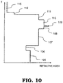
- FIG. 10 shows a refractive index distribution of the cladding region outside the ridge region in the y-direction.
- Equation (3) When a layer thickness d n of the n-type low refractive index layer is 200 nm, v 1 of Equation (3) is 0.292273 at the wavelength of 975 nm. At this time, when a layer thickness d p of the p-type low refractive index layer is 40 nm, v 2 of Equation (3) is 0.149202, the condition v 1 > v 2 holds, and Equation (1), which is the condition disclosed in Patent Document 1, is satisfied.
- the semiconductor laser device shown in FIG. 8 can be regarded as a three-layer slab waveguide having a width W in the x-direction if effective refractive indices of regions I, II, and IIa are known.
- v is obtained from Equation (2), and the number of modes allowed in the x-direction can be known from how many times the value of v is multiplied by ⁇ /2.
- the effective refractive index can be obtained by, for example, the equivalent refractive index method described in Non-Patent Document 3.
- the effective refractive indices of regions I, II, and IIa are obtained to be 3.41738, 3.41600, and 3.41600, respectively.
- the ridge width W is 100 ⁇ m
- the value v is 31.28979
- 20 modes from the zeroth order (fundamental mode) to the nineteenth order are to be allowed.
- the larger the order the wider the divergence angle, and thus the larger the number of allowed modes, the wider the divergence angle.
- the conventional broad area type semiconductor laser device having the ridge shape which satisfies the condition v 1 > v 2 corresponding to the condition disclosed in Patent Document 1, has a problem in that the number of modes allowed in the horizontal direction is large, and thus the divergence angle in the horizontal direction becomes large, and the coupling efficiency with an optical component is low.
- FIG. 1 is a schematic perspective view showing a laminated structure of a semiconductor laser device according to Embodiment 1, that is, a broad area type semiconductor laser device having a ridge shape.
- the semiconductor laser device according to the present embodiment is a semiconductor laser device in which an active layer position in guide layers is shifted from the center of the guide layers to a p-type cladding layer side, thereby reducing the number of carriers staying in the guide layers during operation and increasing a slope efficiency.
- layers comprises, from the bottom thereof, an n-type electrode 1, an n-type GaAs substrate 2 (also, simply referred to as semiconductor substrate), an n-type AlGaAs cladding layer 3 (also, simply referred to as n-type cladding layer or first conductivity type cladding layer, refractive index n c1 ) having an Al composition ratio of 0.20 and a layer thickness of 1.5 ⁇ m, an n-side AlGaAs low refractive index layer 4 (also, referred to as n-side low refractive index layer or first conductivity type low refractive index layer 4, refractive index n 1 ) having the Al composition ratio of 0.25 and the layer thickness d 1 , an n-side AlGaAs second optical guide layer 5 (also, referred to as n-side second optical guide layer or first conductivity type side second optical guide layer) having the Al composition ratio of 0.16 and a layer thickness of 1100 nm, an n-side AlGaA
- n-side second optical guide layer 5 and the n-side first optical guide layer 6 is also collectively referred to as n-side optical guide layer 56 or first conductivity type side optical guide layer 56
- the p-side first optical guide layer 8 and the p-side second optical guide layer 9 is also collectively referred to as p-side optical guide layer 89 or second conductivity type side optical guide layer 89. Since these optical guide layers are usually undoped layers, "side" is added to distinguish which side of the active layer 7 the optical guide layers are on. The reason why the In composition ratio of the InGaAs quantum well active layer 7 is 0.119 and the layer thickness is 8 nm is that the oscillation wavelength is made to be substantially 975 nm.
- a region I is a ridge region having a width W
- regions II and IIa are cladding regions outside the ridge region.
- the conductivity type of the semiconductor substrate 2 may be referred to as first conductivity type, and the conductivity type opposite to that of the semiconductor substrate 2 may be referred to as second conductivity type. That is, if the first conductivity type is n-type, the second conductivity type is p-type, and if the first conductivity type is p-type, the second conductivity type is n-type.
- first conductivity type is n-type and the second conductivity type is p-type
- second conductivity type is n-type
- first conductivity type is described as the n-type
- subscript 1 is attached for parameters relating to the first conductivity type
- the second conductivity type is described as the p-type
- subscript 2 is attached for parameters relating to the second conductivity type.
- the refractive indices of the first conductivity type side optical guide layer 56 and the active layer 7 are higher than those of the second conductivity type side optical guide layer 89, and the refractive index of each of the low refractive index layers is lower than the refractive index of the corresponding cladding layer in contact with. Accordingly, when the refractive indices of the first conductivity type side optical guide layer 56 and the active layer 7 are replaced by the refractive indices of the second conductivity type side optical guide layer 89 and the refractive index of each of the low refractive index layers is replaced by the refractive index of the corresponding cladding layer, v becomes smaller than that of the structure of the present application shown in FIG.
- v of the structure with the replacement allows the first-order or higher-order mode
- the structure of the present application shown in FIG. 1 also necessarily allows the first-order or higher-order mode.
- v of the structure with the replacement is 2.39564, and it can be seen that the structure is such that the zero order mode (fundamental mode) and the first order mode are allowed.
- an average refractive index of the optical guide layers may be calculated in the following manner to obtain the number of allowed modes. Assuming that the refractive index and the layer thickness for the n-side first optical guide layer 6 are n g11 and d g11 , the refractive index and the layer thickness for the n-side second optical guide layer 5 are n g12 and d g12 , the refractive index and the layer thickness for the p-side first optical guide layer 8 are n g21 and d g21 , and the refractive index and the layer thickness for the p-side second optical guide layer 9 are n g22 and d g22 , the average refractive index n gm of the optical guide layers is expressed by Equation (5).
- n gm n g 11 ⁇ d g 11 + n g 12 ⁇ d g 12 + n g 21 ⁇ d g 21 + n g 22 ⁇ d g 22 d g 11 + d g 12 + d g 21 + d g 22
- v is calculated to obtain the number of allowed modes.
- the number of the guide layers is even larger, the number of allowed modes can be obtained in the same manner. Note that, although the active layer 7 is omitted because it is thin, it can be considered into the average refractive index in the same manner.
- an optical confinement rate of the fundamental (zero order) mode is the highest, that is, the gain of the fundamental (zero order) mode is the highest, so that the oscillation in the y-direction is generally in the fundamental (zero order) mode.
- the condition is such that the first-order or higher-order mode is allowed also in the x-direction. That is, when the effective refractive index of the region I which is the ridge region having a width W shown in FIG. 1 is n r and the effective refractive index for cladding regions II and IIa outside the ridge region is n b , the condition is such that a relationship 2 ⁇ ⁇ n r 2 ⁇ n b 2 w 2 > ⁇ 2 is satisfied.
- a structure satisfying this condition is sometimes called a broad area structure.
- v 1 is 0.292273 at a wavelength of 975 nm.
- v 2 is 0.522208, and the condition v 2 > v 1 holds.
- the effective refractive indices of the regions I, II and IIa are determined to be 3.41665, 3.41637, and 3.41637, respectively, and when the ridge width W satisfying the above Equation (6) is 100 ⁇ m, v is 14.09388. As a result, only nine modes from the zeroth order (fundamental mode) to the eighth order are allowed, and no modes higher than the ninth order are allowed.
- the number of modes allowed in the x-direction is smaller and the divergence angle in the horizontal direction can be narrower than by setting the layer thicknesses of the respective layers so that the condition v 2 ⁇ v 1 holds.
- the first conductivity type side optical guide layer 56 is made thicker than the second conductivity type side optical guide layer 89, and the position of the active layer is shifted from the center of the optical guide layers to the second conductivity type cladding layer side, as in the structure of Patent Document 1.
- this structure it is possible to reduce the light absorption by the carriers staying in the optical guide layers during operation and to increase the slope efficiency.
- FIG. 2 is a schematic perspective view showing a laminated structure of a semiconductor laser device according to Embodiment 2.
- Embodiment 2 is an embodiment in which a structure is symmetrical such that the active layer is disposed at the center of the optical guide layers.
- FIG. 2 is a schematic perspective view showing a laminated structure of a semiconductor laser device according to Embodiment 2.
- Embodiment 2 is an embodiment in which a structure is symmetrical such that the active layer is disposed at the center of the optical guide layers.
- the first conductivity type side optical guide layer 56 is composed of an n-side AlGaAs second optical guide layer 5a having the Al composition ratio of 0.16 and a layer thickness of 700 nm and an n-side AlGaAs first optical guide layer 6a having the Al composition ratio of 0.14 and a layer thickness of 200 nm
- the second conductivity type side optical guide layer 89 is composed of a p-side AlGaAs first optical guide layer 8a having the Al composition ratio of 0.14 and a layer thickness of 200 nm and a p-side AlGaAs second optical guide layer 9a having the Al composition ratio of 0.16 and a layer thickness of 700 nm.
- the other layers are the same as in FIG. 1 .
- the parameters of each layer are set so that the condition v 2 > v 1 can hold.
- the condition v 2 > v 1 holds, the case where d 2 is 140 nm is examined. In the case where d 2 is 140 nm, then the condition v 2 > v 1 holds because v 2 is 0.522208.
- the effective refractive indices of the regions I, II, and IIa are determined to be 3.41840, 3.41828, and 3.41828, respectively, and when the ridge width W is 100 ⁇ m, v is 9.229082. As a result, only six modes from the zeroth order (fundamental mode) to the fifth order are allowed.
- v 2 > v 1 it is possible to reduce the number of modes allowed in the horizontal direction as compared with the case where v 2 ⁇ v 1 , and to narrow the divergence angle in the horizontal direction.
- FIG. 3 is a schematic perspective view showing a laminated structure of a semiconductor laser device according to Embodiment 3.
- Embodiment 3 is an embodiment in which a p-type AlGaAs cladding layer 11a having the Al composition ratio of 0.25 and a layer thickness of 1.5 ⁇ m is used as the p-type cladding layer 11 in FIG. 2 of Embodiment 2.
- the refractive index n c1 of the n-type cladding layer 3 first conductivity type cladding layer
- n c2 of the p-type cladding layer 11a second conductivity type cladding layer.
- the other layers are the same as those in FIG. 2 of Embodiment 2.
- v 1 When the layer thickness d 1 of the first conductivity type low refractive index layer 4 is 200 nm, v 1 is 0.292273, and when the layer thickness d 2 of the second conductivity type low refractive index layer 10 is 40 nm, v 2 is 0.137275, and the condition v 2 ⁇ v 1 , which is the condition disclosed in Patent Document 1, holds.
- the effective refractive indices of the regions I, II, and IIa at this time are determined to be 3.41858, 3.41810, and 3.41810, respectively, and if the ridge width W is 100 ⁇ m, v is 18.45816. As a result, 12 modes from the zeroth order (fundamental mode) to the eleventh order are allowed.
- the parameters of each layer are set so that the condition v 2 > v 1 can holds.
- the condition v 2 > v 1 holds, the case where d 2 is 140 nm is examined. When d 2 is 140 nm, then v 2 is 0.480463, and the condition v 2 > v 1 holds.
- the effective refractive indices of the regions I, II, and IIa at this time are determined to be 3.41837, 3.41828, and 3.41828, respectively, and when the ridge width W is 100 ⁇ m, v is 7.992602. As a result, only six modes from the zeroth order (fundamental mode) to the fifth order are allowed.
- the condition v 2 > v 1 it is possible to reduce the number of modes allowed in the horizontal direction as compared with the case where the condition v 2 ⁇ v 1 holds and to narrow the divergence angle in the horizontal direction.
- FIG. 4 is a schematic perspective view showing a laminated structure of a semiconductor laser device according to Embodiment 4.
- the p-type AlGaAs cladding layer 11a having the Al composition ratio of 0.25 and a layer thickness of 1.5 ⁇ m is used as the p-type cladding layer 11 in FIG. 1 of Embodiment 1.
- the other layers are the same as those in Embodiment 1.
- Embodiment 3 by adopting an asymmetric structure in which the refractive index n c1 of the first conductivity type cladding layer 3 is higher than the refractive index n c2 of the second conductivity type cladding layer 11a, light absorption by the carriers in the second conductivity type cladding layer 11a can be reduced.
- the first conductivity type side optical guide layer 56 thicker than the second conductivity type side optical guide layer 89 and the active layer position is shifted from the center of the optical guide layers to the second conductivity type cladding layer side, it is possible to reduce light absorption by the carriers staying in the optical guide layers during operation and to increase the slope efficiency.
- v 1 When the layer thickness d 1 of the first conductivity type low refractive index layer 4 is 200 nm, v 1 is 0.292273, and when the layer thickness d 2 of the second conductivity type low refractive index layer 10 is 40 nm, v 2 is 0.137275, and the condition v 2 ⁇ v 1 , which is the condition disclosed in Patent Document 1, holds.
- the effective refractive indices of the regions I, II, and IIa at this time are determined to be 3.41704, 3.41600, and 3.41600, respectively, and if the ridge width W is 100 ⁇ m, v is 27.16245. As a result, 18 modes from the zeroth order (fundamental mode) to the seventeenth order are allowed.
- the parameters of each layer are set so that the condition v 2 > v 1 can hold.
- the condition v 2 > v 1 holds, the case where d 2 is 140 nm is examined. When d 2 is 140 nm, then v 2 is 0.480463, and the condition v 2 > v 1 holds.
- the effective refractive indices of the regions I, II, and IIa at this time are determined to be 3.41659, 3.41637, and 3.41637, respectively, and when the ridge width W is 100 ⁇ m, v is 12.49284. As a result, only eight modes from zeroth order (fundamental mode) to seventh order are allowed.
- the condition v 2 > v 1 it is possible to reduce the number of modes allowed in the horizontal direction as compared with the case where the condition v 2 ⁇ v 1 holds and to narrow the divergence angle in the horizontal direction.
- FIG. 5 is a schematic perspective view showing a laminated structure of a semiconductor laser device according to Embodiment 5.
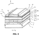
- Embodiment 5 is an example in which the second conductivity type low refractive index layer 10 and the first conductivity type low refractive index layer 4 are disposed inside the second conductivity type cladding layer 11 and the first conductivity type cladding layer 3, respectively.
- the n-type AlGaAs cladding layer 3 having the Al composition ratio of 0.20 is composed of an n-type AlGaAs second cladding layer 3b having a layer thickness of 1.4 ⁇ m and an n-type AlGaAs first cladding layer 3a having a layer thickness of 0.1 ⁇ m, and the n-type low refractive index layer 4 is disposed between the n-type AlGaAs second cladding layer 3b and the n-type AlGaAs first cladding layer 3a.
- the p-type AlGaAs cladding layer 11 having the Al composition ratio of 0.20 is composed of a p-type AlGaAs first cladding layer 11b having a layer thickness of 0.1 ⁇ m and a p-type AlGaAs second cladding layer 11c having a layer thickness of 1.4 ⁇ m, and the second conductivity type low refractive index layer 10 is disposed between the p-type AlGaAs first cladding layer 11b and the p-type AlGaAs second cladding layer 11c.
- the rest is the same as in Embodiment 2.
- v 1 When the layer thickness d 1 of the first conductivity type low refractive index layer 4 is 200 nm, v 1 is 0.292273, and when the layer thickness d 2 of the second conductivity type low refractive index layer 10 is 40 nm, v 2 is 0.149202, and the condition v 2 ⁇ v 1 , which is the condition disclosed in Patent Document 1, holds.
- the effective refractive indices of the regions I, II, and IIa at this time are determined to be 3.41906, 3.41867, and 3.41867, respectively, and when the ridge width W is 100 ⁇ m, v is 16.63924. As a result, 11 modes from the zeroth order (fundamental mode) to the tenth order are allowed.
- the parameters of each layer are set so that v 2 > v 1 can holds.
- the condition v 2 > v 1 holds, the case where d 2 is 140 nm is examined. When d 2 is 140 nm, then v 2 is 0.522208, and the condition v 2 > v 1 holds.
- the effective refractive indices of the regions I, II, and IIa at this time are determined to be 3.41886, 3.41878, and 3.41878, respectively, and when the ridge width W is 100 ⁇ m, v is 7.536043. As a result, only five modes from the zeroth order (fundamental mode) to the fourth order are allowed.
- v 2 > v 1 it is possible to reduce the number of modes allowed in the horizontal direction as compared with the case where the condition v 2 ⁇ v 1 and to narrow the divergence angle in the horizontal direction.
- FIG. 6 is a schematic perspective view showing a laminated structure of a semiconductor laser device according to Embodiment 6.
- Embodiment 6 is an embodiment in which, when forming the ridge, the p-type AlGaAs low refractive index layer 10 outside the ridge region I is removed, and etching is stopped in the p-type AlGaAs first cladding layer 11b. That is, the p-type low refractive index layer 10 (second conductivity type low refractive index layer) is formed only in the ridge region I. The rest is the same as in FIG. 5 of Embodiment 5.
- v 1 When the layer thickness d 1 of the first conductivity type low refractive index layer 4 is 200 nm, v 1 is 0.292273, and when the layer thickness d 2 of the second conductivity type low refractive index layer 10 is 40 nm, v 2 is 0.149202, and the condition v 2 ⁇ v 1 , which is the condition disclosed in Patent Document 1, holds.
- the effective refractive indices of the regions I, II, and IIa at this time are determined to be 3.41906, 3.41857, and 3.41857, respectively, and when the ridge width W is 100 ⁇ m, v is 18.65074. As a result, 12 modes from the zeroth order (fundamental mode) to the eleventh order are allowed.
- the parameters of each layer are set so that v 2 > v 1 can holds.
- the condition v 2 > v 1 holds, the case where d 2 is 140 nm is examined. When d 2 is 140 nm, then v 2 is 0.522208, and the condition v 2 > v 1 holds.
- the effective refractive indices of the regions I, II, and IIa at this time are determined to be 3.41886, 3.41857, and 3.41857, respectively, and when the ridge width W is 100 ⁇ m, v is 14.34798. As a result, only 10 modes from the zeroth order (fundamental mode) to the ninth order are allowed.
- v 2 > v 1 it is possible to reduce the number of modes allowed in the horizontal direction as compared with the case where the condition v 2 ⁇ v 1 holds and to narrow the divergence angle in the horizontal direction.
- condition v 2 > v 1 is held by changing the layer thickness of the p-type low refractive index layer, that is, the second conductivity type low refractive index layer, has been described, but it is possible to holds the condition v 2 > v 1 by changing not only the layer thickness but also the refractive index or by changing both the layer thickness and the refractive index, and thus the effects described in each of the embodiments can be achieved.
- the thickness and the refractive index for the n-type low refractive index layer and the p-type low refractive index layer namely, the first conductivity type low refractive index layer and the second conductivity type low refractive index layer, and the refractive indices for the first conductivity type cladding layer and the second conductivity type cladding layer should be set so as to satisfy Equation (4).
- the semiconductor laser having an oscillation wavelength of 975 nm has been described as an example, but it is needless to say that this wavelength is not a limitation.
- this wavelength is not a limitation.
- a GaN laser in the 400 nm band a GaInP laser in the 600 nm band, and an InGaAsP laser in the 1550 nm band, similar effects can be obtained.
Landscapes
- Physics & Mathematics (AREA)
- Condensed Matter Physics & Semiconductors (AREA)
- General Physics & Mathematics (AREA)
- Electromagnetism (AREA)
- Optics & Photonics (AREA)
- Geometry (AREA)
- Semiconductor Lasers (AREA)
Abstract
Description
- The present application relates to a semiconductor laser device.
- In a semiconductor laser device, particularly a high-power semiconductor laser device, it is required to make the oscillation efficiency as high as possible in order to reduce waste heat and simplify a cooling device. For example,
Patent Document 1 discloses a semiconductor laser device having a high slope efficiency and a high power conversion efficiency at a high output. FIG. 27 ofPatent Document 1 shows a ridge type semiconductor laser device including an optical guide layer thick enough to allow a first-order or higher-order mode in the lamination direction of the crystal, an active layer disposed on a p-type cladding layer side to the center of optical guide layers, an n-type low refractive index layer having a refractive index n11 lower than the refractive index of an n-type cladding layer and a layer thickness d11 between the n-type cladding layer having a refractive index nc and an n-side optical guide layer, and a p-type low refractive index layer having a refractive index n12 lower than the refractive index of the p-type cladding layer and a layer thickness d12 between the p-type cladding layer having the refractive index nc and a p-side optical guide layer, and satisfying the following Equation (1).

- Patent Document 1:
Japanese Unexamined Patent Application Publication No. 2017-84845 -
- Non-Patent Document 1: Written by Kawakami, "Optical Waveguide", Asakura Publishing Co., Ltd, Sep 20th, 1982, pp. 21
- Non-patent Document 2: Edited and written by Iga, "Semiconductor Laser", Ohmsha, Oct. 25th, 1994, pp. 35-38
- Non-Patent Document 3: G. B. Hocker and W. K. Burns, "Mode dispersion in diffused channel waveguides by the effective index method" Appl. Opt. Vol. 16, No. 1. pp. 113-118, 1977
- It has been examined to apply the structure of the semiconductor laser device described in
Patent Document 1 to a broad area type semiconductor laser device having a ridge shape in which a first-order or higher-order mode is allowed in the direction (horizontal direction) perpendicular to the lamination direction of the crystal and the direction of the resonator length, but it has been found that there are problems in that the beam divergence angle in the horizontal direction is widened, the luminance is lowered, and the coupling efficiency with an optical component is low. - The present application discloses a technique for solving the above-mentioned problems, and an object thereof is to obtain a broad area type semiconductor laser device having a ridge shape in which the divergence angle in the horizontal direction is narrowed and the coupling efficiency with an optical component is increased.
- A semiconductor laser device disclosed in the present application includes a first conductivity type cladding layer having a refractive index nc1, a first conductivity type side optical guide layer, an active layer, a second conductivity type side optical guide layer, a second conductivity type cladding layer having a refractive index nc2, and a resonator in which laser light travels back and forth, the above layers being laminated in order on a semiconductor substrate of a first conductivity type, wherein a structure of the device is such that a first-order or higher-order mode is allowed in a lamination direction in a cross section perpendicular to an optical axis direction of the resonator and is a broad area structure in which a first-order or higher-order mode is allowed in a direction perpendicular to the optical axis direction of the resonator and the lamination direction, the broad area structure being with a ridge shape having a ridge region and cladding regions on both sides of the ridge region; and a first conductivity type low refractive index layer having a thickness of d1 and a refractive index n1 lower than nc1 is provided between the first conductivity type side optical guide layer and the first conductivity type cladding layer or inside the first conductivity type cladding layer, a second conductivity type low refractive index layer having a thickness of d2 and a refractive index n2 lower than nc2 is provided between the second conductivity type side optical guide layer and the second conductivity type cladding layer or inside the second conductivity type cladding layer, and a
relationship 
- According to the semiconductor laser device disclosed in the present application, a semiconductor laser device can be obtained in which the number of modes allowed in the horizontal direction can be reduced, the horizontal divergence angle can be narrowed, and a high coupling efficiency with an optical component can be obtained.
-
-
FIG. 1 is a schematic perspective view showing a laminated structure of a semiconductor laser device according toEmbodiment 1. -
FIG. 2 is a schematic perspective view showing a laminated structure of a semiconductor laser device according toEmbodiment 2. -
FIG. 3 is a schematic perspective view showing a laminated structure of a semiconductor laser device according toEmbodiment 3. -
FIG. 4 is a schematic perspective view showing a laminated structure of a semiconductor laser device according toEmbodiment 4. -
FIG. 5 is a schematic perspective view showing a laminated structure of a semiconductor laser device according toEmbodiment 5. -
FIG. 6 is a schematic perspective view showing a laminated structure of a semiconductor laser device according toEmbodiment 6. -
FIG. 7 is a schematic diagram showing a refractive index distribution of an optical waveguide. -
FIG. 8 is a schematic perspective view showing a laminated structure of a semiconductor laser device according to a comparative example. -
FIG. 9 is a diagram for explaining a refractive index distribution in a lamination direction in a ridge region of the structure ofFIG. 8 . -
FIG. 10 is a diagram for explaining a refractive index distribution in the lamination direction in an outer region of the ridge region of the structure ofFIG. 8 . - The phenomenon in which the beam divergence angle in the horizontal direction is widened when the structure of
Patent Document 1 is applied to a broad area type semiconductor laser device was examined in detail, and it was found that the phenomenon is caused by a multimode oscillation in the horizontal direction. Hereinafter, it will be described referring to the drawings.FIG. 7 is a schematic diagram showing a refractive index distribution of an optical waveguide, which will be used for explaining a normalized frequency v. InFIG. 7 , acore region 101 has a refractive index na and a width of t, acladding region 102 and acladding region 102a have a refractive index nb, and a relationship na > nb holds. The normalized frequency v is defined by Equation (2) using an oscillation wavelength λ (refer to Non-Patent Document 1).

- When Equation (2) and Equation (1) is compared, it can be seen that Equation (1) is based on the normalized frequency v. Therefore, when a low refractive index layer having a refractive index ni and a layer thickness di is inserted between a cladding layer and a guide layer that have a refractive index nc, the magnitude relationship shown in Equation (1) is expressed using vi in Equation (3) instead of Equation (1). That is, using the definition of Equation (3), Equation (1), which is the condition disclosed in
Patent Document 1, indicates a condition v1 > v2.
-
FIG. 8 is a schematic perspective view showing a laminated structure of an example in which a technique disclosed inPatent Document 1 is applied to a broad area type semiconductor laser device having a ridge shape with an oscillation wavelength of 975 nm. Layers inFIG. 8 comprises, from the bottom ofFIG. 8 , an n-type electrode 103, an n-type GaAs substrate 104, an n-typeAlGaAs cladding layer 105 having an Al composition ratio of 0.20 and a layer thickness of 1.5 µm, an n-type AlGaAs lowrefractive index layer 106 having the Al composition ratio of 0.25 and the layer thickness d1 (also referred to as n-type low refractive index layer, the refractive index is n1), an n-side AlGaAs secondoptical guide layer 107 having the Al composition ratio of 0.16 and a layer thickness of 1100 nm, an n-side AlGaAs firstoptical guide layer 108 having the Al composition ratio of 0.14 and a layer thickness of 100 nm (the combination of 107 and 108 is also referred to as n-side optical guide layer), an InGaAs quantum wellactive layer 109 having an In composition ratio of 0.119 and a layer thickness of 8 nm, a p-side AlGaAs firstoptical guide layer 110 having the Al composition ratio of 0.14 and a layer thickness of 300 nm, a p-side AlGaAs secondoptical guide layer 111 having the Al composition ratio of 0.16 and a layer thickness of 300 nm (the combination of 110 and 111 is also referred to as p-side optical guide layer), a p-type AlGaAs lowrefractive index layer 112 having the Al composition ratio of 0.55 and a layer thickness d2 (also referred to as p-type low refractive index layer, the refractive index is n2), a p-typeAlGaAs cladding layer 113 having the Al composition ratio of 0.20 and a layer thickness of 1.5 µm, a p-typeGaAs contact layer 114, anSiN film 115 having a film thickness of 0.2 µm, and a p-type electrode 116. The reason why the In composition ratio of the InGaAs quantum well active layer is 0.119 and the layer thickness is 8 nm is that the oscillation wavelength is made to be substantially 975 nm. A region I is a ridge region having a width W, and regions II and IIa are cladding regions outside the ridge region. - Note that surfaces constituting a resonator for making laser light travel back and forth are provided at both ends by, for example, cleavage. As shown in
FIG. 8 , the direction in which the laser light travels back and forth, namely, the optical axis direction of the laser light is the z-direction, the lamination direction of each layer is the y-direction, and the direction perpendicular to the z-direction and the y-direction, namely, the width direction of the ridge is the x-direction. In other figures in the present application, the directions of x, y and z are the same. - Using the refractive index calculation described in
Non-Patent Document 2, the refractive indices of AlGaAs layers having Al composition ratios of 0.14, 0.16, 0.20, 0.25 and 0.55 at the wavelength of 975 nm, for example, are 3.432173, 3.419578, 3.394762, 3.364330 and 3.191285, respectively. Further, the refractive indices of InGaAs having an In composition ratio of 0.119 and SiN are empirically 3.542393 and 2.00, respectively.FIG. 9 shows a refractive index distribution of the ridge region in the y-direction, andFIG. 10 shows a refractive index distribution of the cladding region outside the ridge region in the y-direction. - When a layer thickness dn of the n-type low refractive index layer is 200 nm, v1 of Equation (3) is 0.292273 at the wavelength of 975 nm. At this time, when a layer thickness dp of the p-type low refractive index layer is 40 nm, v2 of Equation (3) is 0.149202, the condition v1 > v2 holds, and Equation (1), which is the condition disclosed in
Patent Document 1, is satisfied. - The semiconductor laser device shown in
FIG. 8 can be regarded as a three-layer slab waveguide having a width W in the x-direction if effective refractive indices of regions I, II, and IIa are known. In this case, v is obtained from Equation (2), and the number of modes allowed in the x-direction can be known from how many times the value of v is multiplied by π/2. The effective refractive index can be obtained by, for example, the equivalent refractive index method described in Non-PatentDocument 3. In the case of the semiconductor laser device shown inFIG. 8 , the effective refractive indices of regions I, II, and IIa are obtained to be 3.41738, 3.41600, and 3.41600, respectively. Assuming that the ridge width W is 100 µm, the value v is 31.28979, and 20 modes from the zeroth order (fundamental mode) to the nineteenth order are to be allowed. The larger the order, the wider the divergence angle, and thus the larger the number of allowed modes, the wider the divergence angle. - As described above, it has been clarified that the conventional broad area type semiconductor laser device having the ridge shape, which satisfies the condition v1 > v2 corresponding to the condition disclosed in
Patent Document 1, has a problem in that the number of modes allowed in the horizontal direction is large, and thus the divergence angle in the horizontal direction becomes large, and the coupling efficiency with an optical component is low. - On the basis of the above examination result, results obtained by examining structures in which the number of modes allowed in the horizontal direction is small will be described in each of embodiments.
-
FIG. 1 is a schematic perspective view showing a laminated structure of a semiconductor laser device according toEmbodiment 1, that is, a broad area type semiconductor laser device having a ridge shape. The semiconductor laser device according to the present embodiment is a semiconductor laser device in which an active layer position in guide layers is shifted from the center of the guide layers to a p-type cladding layer side, thereby reducing the number of carriers staying in the guide layers during operation and increasing a slope efficiency. - In
FIG. 1 , layers comprises, from the bottom thereof, an n-type electrode 1, an n-type GaAs substrate 2 (also, simply referred to as semiconductor substrate), an n-type AlGaAs cladding layer 3 (also, simply referred to as n-type cladding layer or first conductivity type cladding layer, refractive index nc1) having an Al composition ratio of 0.20 and a layer thickness of 1.5 µm, an n-side AlGaAs low refractive index layer 4 (also, referred to as n-side low refractive index layer or first conductivity type low refractive index layer 4, refractive index n1) having the Al composition ratio of 0.25 and the layer thickness d1, an n-side AlGaAs second optical guide layer 5 (also, referred to as n-side second optical guide layer or first conductivity type side second optical guide layer) having the Al composition ratio of 0.16 and a layer thickness of 1100 nm, an n-side AlGaAs first optical guide layer 6 (also, referred to as n-side first optical guide layer or first conductivity type side first optical guide layer) having the Al composition ratio of 0.14 and a layer thickness of 100 nm, an InGaAs quantum well active layer 7 having an In composition ratio of 0.119 and a layer thickness of 8 nm, a p-side AlGaAs first optical guide layer 8 (also, referred to as p-side first optical guide layer or second conductivity type side first optical guide layer) having the Al composition ratio of 0.14 and a layer thickness of 300 nm, a p-side AlGaAs second optical guide layer 9 (also, referred to as p-side second optical guide layer or second conductivity type side second optical guide layer) having the Al composition ratio of 0.16 and a layer thickness of 300 nm, a p-type AlGaAs low refractive index layer 10 (also, referred to as p-type low refractive index layer or second conductivity type low refractive index layer, refractive index n2) having the Al composition ratio of 0.55 and the layer thickness d2, a p-type AlGaAs cladding layer 11 (also, referred to as p-type cladding layer or second conductivity type cladding layer, refractive index nc2) having the Al composition ratio of 0.20 and a layer thickness of 1.5 µm, a p-type GaAs contact layer 12, a SiN film 13 having a film thickness of 0.2 µm, and a p-type electrode 14. Note that the n-side secondoptical guide layer 5 and the n-side firstoptical guide layer 6 is also collectively referred to as n-sideoptical guide layer 56 or first conductivity type sideoptical guide layer 56, and the p-side firstoptical guide layer 8 and the p-side secondoptical guide layer 9 is also collectively referred to as p-sideoptical guide layer 89 or second conductivity type sideoptical guide layer 89. Since these optical guide layers are usually undoped layers, "side" is added to distinguish which side of theactive layer 7 the optical guide layers are on. The reason why the In composition ratio of the InGaAs quantum wellactive layer 7 is 0.119 and the layer thickness is 8 nm is that the oscillation wavelength is made to be substantially 975 nm. A region I is a ridge region having a width W, and regions II and IIa are cladding regions outside the ridge region. - In the description of the present application, a structure in which a ridge structure is formed on the p-type contact layer side by using the
semiconductor substrate 2 of the n-type is described, but to the contrary, a similar effect can be obtained by forming the ridge on the n-type contact layer side by using thesemiconductor substrate 2 of the p-type. The conductivity type of thesemiconductor substrate 2 may be referred to as first conductivity type, and the conductivity type opposite to that of thesemiconductor substrate 2 may be referred to as second conductivity type. That is, if the first conductivity type is n-type, the second conductivity type is p-type, and if the first conductivity type is p-type, the second conductivity type is n-type. In each of the embodiments, a structure in which the first conductivity type is n-type and the second conductivity type is p-type is described as an example, but a structure in which the first conductivity type is p-type and the second conductivity type is n-type may be adopted. In the present application, the first conductivity type is described as the n-type, and thus thesubscript 1 is attached for parameters relating to the first conductivity type, and the second conductivity type is described as the p-type, and thus thesubscript 2 is attached for parameters relating to the second conductivity type. As described above, since these optical guide layers are usually undoped layers, "side" is added to distinguish which side of theactive layer 7 the optical guide layers are on. - Although the main structure of the layers of the semiconductor laser device shown in
FIG. 1 is the same as that shown inFIG. 8 , as described below, the layer thicknesses and the refractive indices for the first conductivity type lowrefractive index layer 4 and the second conductivity type lowrefractive index layer 10, and the refractive indices for the first conductivitytype cladding layer 3 and the second conductivitytype cladding layer 11 are set so as to hold a condition v2 > v1, that is,
- First, the number of modes in the y-direction is examined. The refractive indices of the first conductivity type side
optical guide layer 56 and theactive layer 7 are higher than those of the second conductivity type sideoptical guide layer 89, and the refractive index of each of the low refractive index layers is lower than the refractive index of the corresponding cladding layer in contact with. Accordingly, when the refractive indices of the first conductivity type sideoptical guide layer 56 and theactive layer 7 are replaced by the refractive indices of the second conductivity type sideoptical guide layer 89 and the refractive index of each of the low refractive index layers is replaced by the refractive index of the corresponding cladding layer, v becomes smaller than that of the structure of the present application shown inFIG. 1 . Therefore, if v of the structure with the replacement allows the first-order or higher-order mode, the structure of the present application shown inFIG. 1 also necessarily allows the first-order or higher-order mode. FromFIG. 7 and Equation (2), v of the structure with the replacement is 2.39564, and it can be seen that the structure is such that the zero order mode (fundamental mode) and the first order mode are allowed. - More precisely, an average refractive index of the optical guide layers may be calculated in the following manner to obtain the number of allowed modes. Assuming that the refractive index and the layer thickness for the n-side first
optical guide layer 6 are ng11 and dg11, the refractive index and the layer thickness for the n-side secondoptical guide layer 5 are ng12 and dg12, the refractive index and the layer thickness for the p-side firstoptical guide layer 8 are ng21 and dg21, and the refractive index and the layer thickness for the p-side secondoptical guide layer 9 are ng22 and dg22, the average refractive index ngm of the optical guide layers is expressed by Equation (5).

- By substituting ngm for na, the refractive index of the cladding layers for nb, and dg11 + dg12 + dg21 + dg22 for t in Equation (2), v is calculated to obtain the number of allowed modes. When the number of the guide layers is even larger, the number of allowed modes can be obtained in the same manner. Note that, although the
active layer 7 is omitted because it is thin, it can be considered into the average refractive index in the same manner. In the y-direction, even when a higher order mode is allowed, an optical confinement rate of the fundamental (zero order) mode is the highest, that is, the gain of the fundamental (zero order) mode is the highest, so that the oscillation in the y-direction is generally in the fundamental (zero order) mode. - Next, the number of modes in the x-direction is examined. In the semiconductor laser device disclosed in the present application, the condition is such that the first-order or higher-order mode is allowed also in the x-direction. That is, when the effective refractive index of the region I which is the ridge region having a width W shown in
FIG. 1 is nr and the effective refractive index for cladding regions II and IIa outside the ridge region is nb, the condition is such that arelationship 
- When the layer thickness d1 of the first conductivity type low
refractive index layer 4 is 200 nm, v1 is 0.292273 at a wavelength of 975 nm. At this time, when the layer thickness d2 of the second conductivity type lowrefractive index layer 10 is 140 nm, v2 is 0.522208, and the condition v2 > v1 holds. The effective refractive indices of the regions I, II and IIa are determined to be 3.41665, 3.41637, and 3.41637, respectively, and when the ridge width W satisfying the above Equation (6) is 100 µm, v is 14.09388. As a result, only nine modes from the zeroth order (fundamental mode) to the eighth order are allowed, and no modes higher than the ninth order are allowed. - As described above, when d2 is 40 nm, which satisfies the condition v2 < v1 disclosed in
Patent Document 1, 20 modes are allowed as the mode in the x-direction, whereas when d2 is 140 nm, which satisfies the condition v2 > v1 disclosed in the present application, nine modes are allowed as the mode in the x-direction and thus the number of modes allowed in the x-direction can be reduced to half or less. That is, by setting the layer thicknesses of d2 and d1 so that the condition v2 > v1 holds, the number of modes allowed in the x-direction is smaller and the divergence angle in the horizontal direction can be narrower than by setting the layer thicknesses of the respective layers so that the condition v2 < v1 holds. - Note that, in
Embodiment 1, the first conductivity type sideoptical guide layer 56 is made thicker than the second conductivity type sideoptical guide layer 89, and the position of the active layer is shifted from the center of the optical guide layers to the second conductivity type cladding layer side, as in the structure ofPatent Document 1. With this structure, it is possible to reduce the light absorption by the carriers staying in the optical guide layers during operation and to increase the slope efficiency. -
FIG. 2 is a schematic perspective view showing a laminated structure of a semiconductor laser device according toEmbodiment 2.Embodiment 2 is an embodiment in which a structure is symmetrical such that the active layer is disposed at the center of the optical guide layers. InFIG. 2 , the first conductivity type sideoptical guide layer 56 is composed of an n-side AlGaAs secondoptical guide layer 5a having the Al composition ratio of 0.16 and a layer thickness of 700 nm and an n-side AlGaAs firstoptical guide layer 6a having the Al composition ratio of 0.14 and a layer thickness of 200 nm, and the second conductivity type sideoptical guide layer 89 is composed of a p-side AlGaAs firstoptical guide layer 8a having the Al composition ratio of 0.14 and a layer thickness of 200 nm and a p-side AlGaAs secondoptical guide layer 9a having the Al composition ratio of 0.16 and a layer thickness of 700 nm. The other layers are the same as inFIG. 1 . - In the structure described above, when the layer thickness d1 of the first conductivity type low
refractive index layer 4 is 200 nm, v1 is 0.292273, and when the layer thickness d2 of the second conductivity type lowrefractive index layer 10 is 40 nm, v2 is 0.149202, and the condition v2 < v1, which is the condition disclosed inPatent Document 1, holds. The effective refractive indices of the regions I, II, and IIa at this time are determined to be 3.41873, 3.41810, and 3.41810, respectively, and when the ridge width W is 100 µm, v is 21.14672. As a result, 14 modes from the zeroth order (fundamental mode) to the thirteenth order are allowed. - On the other hand, in
Embodiment 2, the parameters of each layer are set so that the condition v2 > v1 can hold. As an example where the condition v2 > v1 holds, the case where d2 is 140 nm is examined. In the case where d2 is 140 nm, then the condition v2 > v1 holds because v2 is 0.522208. The effective refractive indices of the regions I, II, and IIa are determined to be 3.41840, 3.41828, and 3.41828, respectively, and when the ridge width W is 100 µm, v is 9.229082. As a result, only six modes from the zeroth order (fundamental mode) to the fifth order are allowed. By setting v2 > v1, it is possible to reduce the number of modes allowed in the horizontal direction as compared with the case where v2 < v1, and to narrow the divergence angle in the horizontal direction. -
FIG. 3 is a schematic perspective view showing a laminated structure of a semiconductor laser device according toEmbodiment 3.Embodiment 3 is an embodiment in which a p-typeAlGaAs cladding layer 11a having the Al composition ratio of 0.25 and a layer thickness of 1.5 µm is used as the p-type cladding layer 11 inFIG. 2 ofEmbodiment 2. With this structure, the refractive index nc1 of the n-type cladding layer 3 (first conductivity type cladding layer) can be made higher than the refractive index nc2 of the p-type cladding layer 11a (second conductivity type cladding layer). The other layers are the same as those inFIG. 2 ofEmbodiment 2. By adopting an asymmetric structure in which the refractive index nc1 of the first conductivitytype cladding layer 3 is made higher than the refractive index nc2 of the second conductivitytype cladding layer 11a, light absorption by the carriers in the second conductivitytype cladding layer 11a can be reduced and the slope efficiency can be increased. - When the layer thickness d1 of the first conductivity type low
refractive index layer 4 is 200 nm, v1 is 0.292273, and when the layer thickness d2 of the second conductivity type lowrefractive index layer 10 is 40 nm, v2 is 0.137275, and the condition v2 < v1, which is the condition disclosed inPatent Document 1, holds. The effective refractive indices of the regions I, II, and IIa at this time are determined to be 3.41858, 3.41810, and 3.41810, respectively, and if the ridge width W is 100 µm, v is 18.45816. As a result, 12 modes from the zeroth order (fundamental mode) to the eleventh order are allowed. - On the other hand, in
Embodiment 3, the parameters of each layer are set so that the condition v2 > v1 can holds. As an example where the condition v2 > v1 holds, the case where d2 is 140 nm is examined. When d2 is 140 nm, then v2 is 0.480463, and the condition v2 > v1 holds. The effective refractive indices of the regions I, II, and IIa at this time are determined to be 3.41837, 3.41828, and 3.41828, respectively, and when the ridge width W is 100 µm, v is 7.992602. As a result, only six modes from the zeroth order (fundamental mode) to the fifth order are allowed. By setting the condition v2 > v1, it is possible to reduce the number of modes allowed in the horizontal direction as compared with the case where the condition v2 < v1 holds and to narrow the divergence angle in the horizontal direction. -
FIG. 4 is a schematic perspective view showing a laminated structure of a semiconductor laser device according toEmbodiment 4. InEmbodiment 4, the p-typeAlGaAs cladding layer 11a having the Al composition ratio of 0.25 and a layer thickness of 1.5 µm is used as the p-type cladding layer 11 inFIG. 1 ofEmbodiment 1. The other layers are the same as those inEmbodiment 1. As inEmbodiment 3, by adopting an asymmetric structure in which the refractive index nc1 of the first conductivitytype cladding layer 3 is higher than the refractive index nc2 of the second conductivitytype cladding layer 11a, light absorption by the carriers in the second conductivitytype cladding layer 11a can be reduced. Further, by making the first conductivity type sideoptical guide layer 56 thicker than the second conductivity type sideoptical guide layer 89 and the active layer position is shifted from the center of the optical guide layers to the second conductivity type cladding layer side, it is possible to reduce light absorption by the carriers staying in the optical guide layers during operation and to increase the slope efficiency. - When the layer thickness d1 of the first conductivity type low
refractive index layer 4 is 200 nm, v1 is 0.292273, and when the layer thickness d2 of the second conductivity type lowrefractive index layer 10 is 40 nm, v2 is 0.137275, and the condition v2 < v1, which is the condition disclosed inPatent Document 1, holds. The effective refractive indices of the regions I, II, and IIa at this time are determined to be 3.41704, 3.41600, and 3.41600, respectively, and if the ridge width W is 100 µm, v is 27.16245. As a result, 18 modes from the zeroth order (fundamental mode) to the seventeenth order are allowed. - On the other hand, in
Embodiment 4, the parameters of each layer are set so that the condition v2 > v1 can hold. As an example where the condition v2 > v1 holds, the case where d2 is 140 nm is examined. When d2 is 140 nm, then v2 is 0.480463, and the condition v2 > v1 holds. The effective refractive indices of the regions I, II, and IIa at this time are determined to be 3.41659, 3.41637, and 3.41637, respectively, and when the ridge width W is 100 µm, v is 12.49284. As a result, only eight modes from zeroth order (fundamental mode) to seventh order are allowed. By setting the condition v2 > v1, it is possible to reduce the number of modes allowed in the horizontal direction as compared with the case where the condition v2 < v1 holds and to narrow the divergence angle in the horizontal direction. -
FIG. 5 is a schematic perspective view showing a laminated structure of a semiconductor laser device according toEmbodiment 5.Embodiment 5 is an example in which the second conductivity type lowrefractive index layer 10 and the first conductivity type lowrefractive index layer 4 are disposed inside the second conductivitytype cladding layer 11 and the first conductivitytype cladding layer 3, respectively. In the figure, the n-typeAlGaAs cladding layer 3 having the Al composition ratio of 0.20 is composed of an n-type AlGaAssecond cladding layer 3b having a layer thickness of 1.4 µm and an n-type AlGaAsfirst cladding layer 3a having a layer thickness of 0.1 µm, and the n-type lowrefractive index layer 4 is disposed between the n-type AlGaAssecond cladding layer 3b and the n-type AlGaAsfirst cladding layer 3a. Further, the p-typeAlGaAs cladding layer 11 having the Al composition ratio of 0.20 is composed of a p-type AlGaAsfirst cladding layer 11b having a layer thickness of 0.1 µm and a p-type AlGaAssecond cladding layer 11c having a layer thickness of 1.4 µm, and the second conductivity type lowrefractive index layer 10 is disposed between the p-type AlGaAsfirst cladding layer 11b and the p-type AlGaAssecond cladding layer 11c. The rest is the same as inEmbodiment 2. - When the layer thickness d1 of the first conductivity type low
refractive index layer 4 is 200 nm, v1 is 0.292273, and when the layer thickness d2 of the second conductivity type lowrefractive index layer 10 is 40 nm, v2 is 0.149202, and the condition v2 < v1, which is the condition disclosed inPatent Document 1, holds. The effective refractive indices of the regions I, II, and IIa at this time are determined to be 3.41906, 3.41867, and 3.41867, respectively, and when the ridge width W is 100 µm, v is 16.63924. As a result, 11 modes from the zeroth order (fundamental mode) to the tenth order are allowed. - On the other hand, in
Embodiment 5, the parameters of each layer are set so that v2 > v1 can holds. As an example where the condition v2 > v1 holds, the case where d2 is 140 nm is examined. When d2 is 140 nm, then v2 is 0.522208, and the condition v2 > v1 holds. The effective refractive indices of the regions I, II, and IIa at this time are determined to be 3.41886, 3.41878, and 3.41878, respectively, and when the ridge width W is 100 µm, v is 7.536043. As a result, only five modes from the zeroth order (fundamental mode) to the fourth order are allowed. By setting v2 > v1, it is possible to reduce the number of modes allowed in the horizontal direction as compared with the case where the condition v2 < v1 and to narrow the divergence angle in the horizontal direction. -
FIG. 6 is a schematic perspective view showing a laminated structure of a semiconductor laser device according toEmbodiment 6.Embodiment 6 is an embodiment in which, when forming the ridge, the p-type AlGaAs lowrefractive index layer 10 outside the ridge region I is removed, and etching is stopped in the p-type AlGaAsfirst cladding layer 11b. That is, the p-type low refractive index layer 10 (second conductivity type low refractive index layer) is formed only in the ridge region I. The rest is the same as inFIG. 5 ofEmbodiment 5. - When the layer thickness d1 of the first conductivity type low
refractive index layer 4 is 200 nm, v1 is 0.292273, and when the layer thickness d2 of the second conductivity type lowrefractive index layer 10 is 40 nm, v2 is 0.149202, and the condition v2 < v1, which is the condition disclosed inPatent Document 1, holds. The effective refractive indices of the regions I, II, and IIa at this time are determined to be 3.41906, 3.41857, and 3.41857, respectively, and when the ridge width W is 100 µm, v is 18.65074. As a result, 12 modes from the zeroth order (fundamental mode) to the eleventh order are allowed. - On the other hand, in
Embodiment 6, the parameters of each layer are set so that v2 > v1 can holds. As an example in which the condition v2 > v1 holds, the case where d2 is 140 nm is examined. When d2 is 140 nm, then v2 is 0.522208, and the condition v2 > v1 holds. The effective refractive indices of the regions I, II, and IIa at this time are determined to be 3.41886, 3.41857, and 3.41857, respectively, and when the ridge width W is 100 µm, v is 14.34798. As a result, only 10 modes from the zeroth order (fundamental mode) to the ninth order are allowed. By setting v2 > v1, it is possible to reduce the number of modes allowed in the horizontal direction as compared with the case where the condition v2 < v1 holds and to narrow the divergence angle in the horizontal direction. - In each of the above-described embodiments, the case where the condition v2 > v1 is held by changing the layer thickness of the p-type low refractive index layer, that is, the second conductivity type low refractive index layer, has been described, but it is possible to holds the condition v2 > v1 by changing not only the layer thickness but also the refractive index or by changing both the layer thickness and the refractive index, and thus the effects described in each of the embodiments can be achieved. That is, the thickness and the refractive index for the n-type low refractive index layer and the p-type low refractive index layer, namely, the first conductivity type low refractive index layer and the second conductivity type low refractive index layer, and the refractive indices for the first conductivity type cladding layer and the second conductivity type cladding layer should be set so as to satisfy Equation (4).
- In each of the above-described embodiments, the semiconductor laser having an oscillation wavelength of 975 nm has been described as an example, but it is needless to say that this wavelength is not a limitation. For example, in a GaN laser in the 400 nm band, a GaInP laser in the 600 nm band, and an InGaAsP laser in the 1550 nm band, similar effects can be obtained.
- Note that, although various exemplary embodiments and examples are described in the present application, various features, aspects, and functions described in one or more embodiments are not inherent in a particular embodiment and can be applicable alone or in their various combinations to each embodiment. Accordingly, countless variations that are not illustrated are envisaged within the scope of the art disclosed herein. For example, the case where at least one component is modified, added or omitted, and the case where at least one component is extracted and combined with a component in another embodiment are included.
- 2 semiconductor substrate, 3 first conductivity type cladding layer, 4 first conductivity type low refractive index layer, 56 first conductivity type side optical guide layer, 7 active layer, 89 second conductivity type side optical guide layer, 10 second conductivity type low refractive index layer, 11 second conductivity type cladding layer, I ridge region, II, IIa cladding region
Claims (4)
- A semiconductor laser device, comprising:a first conductivity type cladding layer having a refractive index nc1;a first conductivity type side optical guide layer;an active layer;a second conductivity type side optical guide layer;a second conductivity type cladding layer having a refractive index nc2; anda resonator in which laser light travels back and forth, the above layers being laminated in order on a semiconductor substrate of a first conductivity type, whereinan oscillation wavelength is λ;a structure of the device is such that a first-order or higher-order mode is allowed in a lamination direction in a cross section perpendicular to an optical axis direction of the resonator and is a broad area structure in which a first-order or higher-order mode is allowed in a direction perpendicular to the optical axis direction of the resonator and the lamination direction, the broad area structure being with a ridge shape having a ridge region and cladding regions on both sides of the ridge region; anda first conductivity type low refractive index layer having a thickness of d1 and a refractive index n1 lower than nc1 is provided between the first conductivity type side optical guide layer and the first conductivity type cladding layer or inside the first conductivity type cladding layer, a second conductivity type low refractive index layer having a thickness of d2 and a refractive index n2 lower than nc2 is provided between the second conductivity type side optical guide layer and the second conductivity type cladding layer or inside the second conductivity type cladding layer, and a relationship

- The semiconductor laser device according to claim 1, wherein a thickness of the first conductivity type side optical guide layer is larger than a thickness of the second conductivity type side optical guide layer.
- The semiconductor laser device according to claim 1 or 2, wherein nc1 is higher than nc2.
- The semiconductor laser device according to any one of claims 1 to 3, wherein the second conductivity type low refractive index layer is formed only in the ridge region.
Applications Claiming Priority (1)
| Application Number | Priority Date | Filing Date | Title |
|---|---|---|---|
| PCT/JP2020/005479 WO2021161438A1 (en) | 2020-02-13 | 2020-02-13 | Semiconductor laser device |
Publications (3)
| Publication Number | Publication Date |
|---|---|
| EP4106118A1 true EP4106118A1 (en) | 2022-12-21 |
| EP4106118A4 EP4106118A4 (en) | 2023-05-10 |
| EP4106118B1 EP4106118B1 (en) | 2024-03-27 |
Family
ID=77291480
Family Applications (1)
| Application Number | Title | Priority Date | Filing Date |
|---|---|---|---|
| EP20919188.1A Active EP4106118B1 (en) | 2020-02-13 | 2020-02-13 | Semiconductor laser device |
Country Status (5)
| Country | Link |
|---|---|
| US (1) | US12542426B2 (en) |
| EP (1) | EP4106118B1 (en) |
| JP (1) | JP7304978B2 (en) |
| CN (1) | CN115088149B (en) |
| WO (1) | WO2021161438A1 (en) |
Families Citing this family (1)
| Publication number | Priority date | Publication date | Assignee | Title |
|---|---|---|---|---|
| JPWO2023074228A1 (en) * | 2021-10-27 | 2023-05-04 |
Family Cites Families (22)
| Publication number | Priority date | Publication date | Assignee | Title |
|---|---|---|---|---|
| US6256330B1 (en) * | 1996-12-02 | 2001-07-03 | Lacomb Ronald Bruce | Gain and index tailored single mode semiconductor laser |
| JP2000332361A (en) * | 1999-05-21 | 2000-11-30 | Pioneer Electronic Corp | Gallium-nitride-based semiconductor luminous element |
| JP2001210910A (en) * | 1999-11-17 | 2001-08-03 | Mitsubishi Electric Corp | Semiconductor laser |
| AU4677501A (en) * | 2000-03-28 | 2001-10-08 | Provost, Fellows And Scholars Of The College Of The Holy And Undivided Trinity Of Queen Elizabeth Near Dublin, The | A laser diode |
| JP2004103679A (en) * | 2002-09-06 | 2004-04-02 | Mitsubishi Chemicals Corp | Semiconductor light emitting device and semiconductor light emitting device module |
| WO2004023614A1 (en) * | 2002-09-06 | 2004-03-18 | Mitsubishi Chemical Corporation | Semiconductor light-emitting device and semiconductor light-emitting device module |
| JP2006032437A (en) * | 2004-07-12 | 2006-02-02 | Sony Corp | Semiconductor laser and optical device using the same |
| KR20060038057A (en) * | 2004-10-29 | 2006-05-03 | 삼성전기주식회사 | Semiconductor laser device and its manufacturing method |
| JP4780999B2 (en) * | 2005-04-14 | 2011-09-28 | 三洋電機株式会社 | Manufacturing method of semiconductor laser device |
| JP2008219051A (en) * | 2008-06-13 | 2008-09-18 | Mitsubishi Electric Corp | Semiconductor laser |
| JP2008219050A (en) * | 2008-06-13 | 2008-09-18 | Mitsubishi Electric Corp | Semiconductor laser |
| US7830938B2 (en) * | 2008-12-15 | 2010-11-09 | Jds Uniphase Corporation | Laser diode |
| JP6123427B2 (en) * | 2013-03-29 | 2017-05-10 | 三菱電機株式会社 | Semiconductor laser device |
| JP6255763B2 (en) * | 2013-07-19 | 2018-01-10 | 三菱電機株式会社 | Semiconductor laser device |
| WO2015092992A1 (en) * | 2013-12-20 | 2015-06-25 | パナソニックIpマネジメント株式会社 | Semiconductor light-emitting element |
| EP3304659B1 (en) * | 2015-06-05 | 2023-03-22 | Iulian Basarab Petrescu-Prahova | Emitter semiconductor laser type of device |
| WO2016199363A1 (en) * | 2015-06-08 | 2016-12-15 | パナソニックIpマネジメント株式会社 | Light emitting element |
| JP6512953B2 (en) * | 2015-06-10 | 2019-05-15 | 三菱電機株式会社 | Semiconductor laser device |
| JP6447456B2 (en) * | 2015-10-22 | 2019-01-09 | 三菱電機株式会社 | Semiconductor laser device |
| JP6753236B2 (en) | 2016-09-13 | 2020-09-09 | 三菱電機株式会社 | Broad area semiconductor laser device |
| CN111095700B (en) * | 2017-09-14 | 2021-12-14 | 三菱电机株式会社 | Semiconductor laser device |
| JP2019079911A (en) * | 2017-10-24 | 2019-05-23 | シャープ株式会社 | Semiconductor laser element |
-
2020
- 2020-02-13 CN CN202080095815.6A patent/CN115088149B/en active Active
- 2020-02-13 EP EP20919188.1A patent/EP4106118B1/en active Active
- 2020-02-13 WO PCT/JP2020/005479 patent/WO2021161438A1/en not_active Ceased
- 2020-02-13 JP JP2021577779A patent/JP7304978B2/en active Active
- 2020-02-13 US US17/758,957 patent/US12542426B2/en active Active
Also Published As
| Publication number | Publication date |
|---|---|
| US20230075645A1 (en) | 2023-03-09 |
| US12542426B2 (en) | 2026-02-03 |
| EP4106118B1 (en) | 2024-03-27 |
| EP4106118A4 (en) | 2023-05-10 |
| CN115088149A (en) | 2022-09-20 |
| WO2021161438A1 (en) | 2021-08-19 |
| CN115088149B (en) | 2024-12-17 |
| JPWO2021161438A1 (en) | 2021-08-19 |
| JP7304978B2 (en) | 2023-07-07 |
Similar Documents
| Publication | Publication Date | Title |
|---|---|---|
| US20070133648A1 (en) | Optical device coupling light propagating in optical waveguide with diffraction grating | |
| US6445722B2 (en) | Single-transverse-mode laser diode with multi-mode waveguide region and manufacturing method of the same | |
| JP2007243019A (en) | Optical semiconductor device | |
| JP3576560B2 (en) | Semiconductor laser device | |
| EP2523279B1 (en) | Wide stripe diode laser with high efficiency and low far-field divergence | |
| JP6665279B2 (en) | Semiconductor laser device | |
| US9871348B2 (en) | Semiconductor laser device | |
| EP4106118B1 (en) | Semiconductor laser device | |
| US7466736B2 (en) | Semiconductor laser diode, semiconductor optical amplifier, and optical communication device | |
| JP2000200940A (en) | Semiconductor laser diode | |
| US6996149B2 (en) | Semiconductor laser device and semiconductor laser module | |
| EP1258062B1 (en) | Semiconductor diode lasers with improved beam divergence | |
| US20060120428A1 (en) | Distributed feedback (DFB) semiconductor laser and fabrication method thereof | |
| EP4220875A1 (en) | Semiconductor laser device | |
| JP2009094410A (en) | Semiconductor optical integrated device and manufacturing method thereof | |
| JP4842983B2 (en) | Semiconductor optical integrated device and manufacturing method thereof | |
| JPH10223966A (en) | Gain-coupled distributed feedback semiconductor laser device | |
| JP5163355B2 (en) | Semiconductor laser device | |
| JP4523131B2 (en) | Semiconductor laser device | |
| US20120195337A1 (en) | Semiconductor laser | |
| JP4971235B2 (en) | Semiconductor optical integrated device | |
| US20240154390A1 (en) | Semiconductor optical element | |
| WO2025212787A1 (en) | Edge-emitting semiconductor broad area laser | |
| JP2003060312A (en) | Semiconductor laser element | |
| JPH08129113A (en) | Spot conversion element |
Legal Events
| Date | Code | Title | Description |
|---|---|---|---|
| STAA | Information on the status of an ep patent application or granted ep patent |
Free format text: STATUS: THE INTERNATIONAL PUBLICATION HAS BEEN MADE |
|
| PUAI | Public reference made under article 153(3) epc to a published international application that has entered the european phase |
Free format text: ORIGINAL CODE: 0009012 |
|
| STAA | Information on the status of an ep patent application or granted ep patent |
Free format text: STATUS: REQUEST FOR EXAMINATION WAS MADE |
|
| 17P | Request for examination filed |
Effective date: 20220531 |
|
| AK | Designated contracting states |
Kind code of ref document: A1 Designated state(s): AL AT BE BG CH CY CZ DE DK EE ES FI FR GB GR HR HU IE IS IT LI LT LU LV MC MK MT NL NO PL PT RO RS SE SI SK SM TR |
|
| A4 | Supplementary search report drawn up and despatched |
Effective date: 20230411 |
|
| RIC1 | Information provided on ipc code assigned before grant |
Ipc: H01S 5/343 20060101ALN20230403BHEP Ipc: H01S 5/32 20060101ALI20230403BHEP Ipc: H01S 5/22 20060101ALI20230403BHEP Ipc: H01S 5/20 20060101AFI20230403BHEP |
|
| DAV | Request for validation of the european patent (deleted) | ||
| DAX | Request for extension of the european patent (deleted) | ||
| GRAP | Despatch of communication of intention to grant a patent |
Free format text: ORIGINAL CODE: EPIDOSNIGR1 |
|
| STAA | Information on the status of an ep patent application or granted ep patent |
Free format text: STATUS: GRANT OF PATENT IS INTENDED |
|
| RIC1 | Information provided on ipc code assigned before grant |
Ipc: H01S 5/343 20060101ALN20231130BHEP Ipc: H01S 5/32 20060101ALI20231130BHEP Ipc: H01S 5/22 20060101ALI20231130BHEP Ipc: H01S 5/20 20060101AFI20231130BHEP |
|
| RIC1 | Information provided on ipc code assigned before grant |
Ipc: H01S 5/343 20060101ALN20231201BHEP Ipc: H01S 5/32 20060101ALI20231201BHEP Ipc: H01S 5/22 20060101ALI20231201BHEP Ipc: H01S 5/20 20060101AFI20231201BHEP |
|
| INTG | Intention to grant announced |
Effective date: 20231218 |
|
| GRAS | Grant fee paid |
Free format text: ORIGINAL CODE: EPIDOSNIGR3 |
|
| GRAA | (expected) grant |
Free format text: ORIGINAL CODE: 0009210 |
|
| STAA | Information on the status of an ep patent application or granted ep patent |
Free format text: STATUS: THE PATENT HAS BEEN GRANTED |
|
| AK | Designated contracting states |
Kind code of ref document: B1 Designated state(s): AL AT BE BG CH CY CZ DE DK EE ES FI FR GB GR HR HU IE IS IT LI LT LU LV MC MK MT NL NO PL PT RO RS SE SI SK SM TR |
|
| REG | Reference to a national code |
Ref country code: GB Ref legal event code: FG4D |
|
| REG | Reference to a national code |
Ref country code: CH Ref legal event code: EP |
|
| REG | Reference to a national code |
Ref country code: DE Ref legal event code: R096 Ref document number: 602020028128 Country of ref document: DE |
|
| REG | Reference to a national code |
Ref country code: IE Ref legal event code: FG4D |
|
| PG25 | Lapsed in a contracting state [announced via postgrant information from national office to epo] |
Ref country code: LT Free format text: LAPSE BECAUSE OF FAILURE TO SUBMIT A TRANSLATION OF THE DESCRIPTION OR TO PAY THE FEE WITHIN THE PRESCRIBED TIME-LIMIT Effective date: 20240327 |
|
| REG | Reference to a national code |
Ref country code: LT Ref legal event code: MG9D |
|
| PG25 | Lapsed in a contracting state [announced via postgrant information from national office to epo] |
Ref country code: GR Free format text: LAPSE BECAUSE OF FAILURE TO SUBMIT A TRANSLATION OF THE DESCRIPTION OR TO PAY THE FEE WITHIN THE PRESCRIBED TIME-LIMIT Effective date: 20240628 |
|
| PG25 | Lapsed in a contracting state [announced via postgrant information from national office to epo] |
Ref country code: RS Free format text: LAPSE BECAUSE OF FAILURE TO SUBMIT A TRANSLATION OF THE DESCRIPTION OR TO PAY THE FEE WITHIN THE PRESCRIBED TIME-LIMIT Effective date: 20240627 Ref country code: HR Free format text: LAPSE BECAUSE OF FAILURE TO SUBMIT A TRANSLATION OF THE DESCRIPTION OR TO PAY THE FEE WITHIN THE PRESCRIBED TIME-LIMIT Effective date: 20240327 |
|
| PG25 | Lapsed in a contracting state [announced via postgrant information from national office to epo] |
Ref country code: RS Free format text: LAPSE BECAUSE OF FAILURE TO SUBMIT A TRANSLATION OF THE DESCRIPTION OR TO PAY THE FEE WITHIN THE PRESCRIBED TIME-LIMIT Effective date: 20240627 Ref country code: NO Free format text: LAPSE BECAUSE OF FAILURE TO SUBMIT A TRANSLATION OF THE DESCRIPTION OR TO PAY THE FEE WITHIN THE PRESCRIBED TIME-LIMIT Effective date: 20240627 Ref country code: LT Free format text: LAPSE BECAUSE OF FAILURE TO SUBMIT A TRANSLATION OF THE DESCRIPTION OR TO PAY THE FEE WITHIN THE PRESCRIBED TIME-LIMIT Effective date: 20240327 Ref country code: HR Free format text: LAPSE BECAUSE OF FAILURE TO SUBMIT A TRANSLATION OF THE DESCRIPTION OR TO PAY THE FEE WITHIN THE PRESCRIBED TIME-LIMIT Effective date: 20240327 Ref country code: GR Free format text: LAPSE BECAUSE OF FAILURE TO SUBMIT A TRANSLATION OF THE DESCRIPTION OR TO PAY THE FEE WITHIN THE PRESCRIBED TIME-LIMIT Effective date: 20240628 Ref country code: FI Free format text: LAPSE BECAUSE OF FAILURE TO SUBMIT A TRANSLATION OF THE DESCRIPTION OR TO PAY THE FEE WITHIN THE PRESCRIBED TIME-LIMIT Effective date: 20240327 Ref country code: BG Free format text: LAPSE BECAUSE OF FAILURE TO SUBMIT A TRANSLATION OF THE DESCRIPTION OR TO PAY THE FEE WITHIN THE PRESCRIBED TIME-LIMIT Effective date: 20240327 |
|
| REG | Reference to a national code |
Ref country code: NL Ref legal event code: MP Effective date: 20240327 |
|
| PG25 | Lapsed in a contracting state [announced via postgrant information from national office to epo] |
Ref country code: SE Free format text: LAPSE BECAUSE OF FAILURE TO SUBMIT A TRANSLATION OF THE DESCRIPTION OR TO PAY THE FEE WITHIN THE PRESCRIBED TIME-LIMIT Effective date: 20240327 Ref country code: LV Free format text: LAPSE BECAUSE OF FAILURE TO SUBMIT A TRANSLATION OF THE DESCRIPTION OR TO PAY THE FEE WITHIN THE PRESCRIBED TIME-LIMIT Effective date: 20240327 |
|
| PG25 | Lapsed in a contracting state [announced via postgrant information from national office to epo] |
Ref country code: NL Free format text: LAPSE BECAUSE OF FAILURE TO SUBMIT A TRANSLATION OF THE DESCRIPTION OR TO PAY THE FEE WITHIN THE PRESCRIBED TIME-LIMIT Effective date: 20240327 |
|
| REG | Reference to a national code |
Ref country code: AT Ref legal event code: MK05 Ref document number: 1670842 Country of ref document: AT Kind code of ref document: T Effective date: 20240327 |
|
| PG25 | Lapsed in a contracting state [announced via postgrant information from national office to epo] |
Ref country code: NL Free format text: LAPSE BECAUSE OF FAILURE TO SUBMIT A TRANSLATION OF THE DESCRIPTION OR TO PAY THE FEE WITHIN THE PRESCRIBED TIME-LIMIT Effective date: 20240327 |
|
| PG25 | Lapsed in a contracting state [announced via postgrant information from national office to epo] |
Ref country code: IS Free format text: LAPSE BECAUSE OF FAILURE TO SUBMIT A TRANSLATION OF THE DESCRIPTION OR TO PAY THE FEE WITHIN THE PRESCRIBED TIME-LIMIT Effective date: 20240727 |
|
| PG25 | Lapsed in a contracting state [announced via postgrant information from national office to epo] |
Ref country code: SM Free format text: LAPSE BECAUSE OF FAILURE TO SUBMIT A TRANSLATION OF THE DESCRIPTION OR TO PAY THE FEE WITHIN THE PRESCRIBED TIME-LIMIT Effective date: 20240327 Ref country code: PT Free format text: LAPSE BECAUSE OF FAILURE TO SUBMIT A TRANSLATION OF THE DESCRIPTION OR TO PAY THE FEE WITHIN THE PRESCRIBED TIME-LIMIT Effective date: 20240729 |
|
| PG25 | Lapsed in a contracting state [announced via postgrant information from national office to epo] |
Ref country code: ES Free format text: LAPSE BECAUSE OF FAILURE TO SUBMIT A TRANSLATION OF THE DESCRIPTION OR TO PAY THE FEE WITHIN THE PRESCRIBED TIME-LIMIT Effective date: 20240327 |
|
| PG25 | Lapsed in a contracting state [announced via postgrant information from national office to epo] |
Ref country code: EE Free format text: LAPSE BECAUSE OF FAILURE TO SUBMIT A TRANSLATION OF THE DESCRIPTION OR TO PAY THE FEE WITHIN THE PRESCRIBED TIME-LIMIT Effective date: 20240327 Ref country code: CZ Free format text: LAPSE BECAUSE OF FAILURE TO SUBMIT A TRANSLATION OF THE DESCRIPTION OR TO PAY THE FEE WITHIN THE PRESCRIBED TIME-LIMIT Effective date: 20240327 |
|
| PG25 | Lapsed in a contracting state [announced via postgrant information from national office to epo] |
Ref country code: AT Free format text: LAPSE BECAUSE OF FAILURE TO SUBMIT A TRANSLATION OF THE DESCRIPTION OR TO PAY THE FEE WITHIN THE PRESCRIBED TIME-LIMIT Effective date: 20240327 |
|
| PG25 | Lapsed in a contracting state [announced via postgrant information from national office to epo] |
Ref country code: PL Free format text: LAPSE BECAUSE OF FAILURE TO SUBMIT A TRANSLATION OF THE DESCRIPTION OR TO PAY THE FEE WITHIN THE PRESCRIBED TIME-LIMIT Effective date: 20240327 |
|
| PG25 | Lapsed in a contracting state [announced via postgrant information from national office to epo] |
Ref country code: SK Free format text: LAPSE BECAUSE OF FAILURE TO SUBMIT A TRANSLATION OF THE DESCRIPTION OR TO PAY THE FEE WITHIN THE PRESCRIBED TIME-LIMIT Effective date: 20240327 |
|
| PG25 | Lapsed in a contracting state [announced via postgrant information from national office to epo] |
Ref country code: SM Free format text: LAPSE BECAUSE OF FAILURE TO SUBMIT A TRANSLATION OF THE DESCRIPTION OR TO PAY THE FEE WITHIN THE PRESCRIBED TIME-LIMIT Effective date: 20240327 Ref country code: SK Free format text: LAPSE BECAUSE OF FAILURE TO SUBMIT A TRANSLATION OF THE DESCRIPTION OR TO PAY THE FEE WITHIN THE PRESCRIBED TIME-LIMIT Effective date: 20240327 Ref country code: RO Free format text: LAPSE BECAUSE OF FAILURE TO SUBMIT A TRANSLATION OF THE DESCRIPTION OR TO PAY THE FEE WITHIN THE PRESCRIBED TIME-LIMIT Effective date: 20240327 Ref country code: PT Free format text: LAPSE BECAUSE OF FAILURE TO SUBMIT A TRANSLATION OF THE DESCRIPTION OR TO PAY THE FEE WITHIN THE PRESCRIBED TIME-LIMIT Effective date: 20240729 Ref country code: PL Free format text: LAPSE BECAUSE OF FAILURE TO SUBMIT A TRANSLATION OF THE DESCRIPTION OR TO PAY THE FEE WITHIN THE PRESCRIBED TIME-LIMIT Effective date: 20240327 Ref country code: IS Free format text: LAPSE BECAUSE OF FAILURE TO SUBMIT A TRANSLATION OF THE DESCRIPTION OR TO PAY THE FEE WITHIN THE PRESCRIBED TIME-LIMIT Effective date: 20240727 Ref country code: ES Free format text: LAPSE BECAUSE OF FAILURE TO SUBMIT A TRANSLATION OF THE DESCRIPTION OR TO PAY THE FEE WITHIN THE PRESCRIBED TIME-LIMIT Effective date: 20240327 Ref country code: EE Free format text: LAPSE BECAUSE OF FAILURE TO SUBMIT A TRANSLATION OF THE DESCRIPTION OR TO PAY THE FEE WITHIN THE PRESCRIBED TIME-LIMIT Effective date: 20240327 Ref country code: CZ Free format text: LAPSE BECAUSE OF FAILURE TO SUBMIT A TRANSLATION OF THE DESCRIPTION OR TO PAY THE FEE WITHIN THE PRESCRIBED TIME-LIMIT Effective date: 20240327 Ref country code: AT Free format text: LAPSE BECAUSE OF FAILURE TO SUBMIT A TRANSLATION OF THE DESCRIPTION OR TO PAY THE FEE WITHIN THE PRESCRIBED TIME-LIMIT Effective date: 20240327 |
|
| P01 | Opt-out of the competence of the unified patent court (upc) registered |
Free format text: CASE NUMBER: APP_55724/2024 Effective date: 20241011 |
|
| PG25 | Lapsed in a contracting state [announced via postgrant information from national office to epo] |
Ref country code: IT Free format text: LAPSE BECAUSE OF FAILURE TO SUBMIT A TRANSLATION OF THE DESCRIPTION OR TO PAY THE FEE WITHIN THE PRESCRIBED TIME-LIMIT Effective date: 20240327 |
|
| PG25 | Lapsed in a contracting state [announced via postgrant information from national office to epo] |
Ref country code: IT Free format text: LAPSE BECAUSE OF FAILURE TO SUBMIT A TRANSLATION OF THE DESCRIPTION OR TO PAY THE FEE WITHIN THE PRESCRIBED TIME-LIMIT Effective date: 20240327 |
|
| REG | Reference to a national code |
Ref country code: DE Ref legal event code: R097 Ref document number: 602020028128 Country of ref document: DE |
|
| PG25 | Lapsed in a contracting state [announced via postgrant information from national office to epo] |
Ref country code: DK Free format text: LAPSE BECAUSE OF FAILURE TO SUBMIT A TRANSLATION OF THE DESCRIPTION OR TO PAY THE FEE WITHIN THE PRESCRIBED TIME-LIMIT Effective date: 20240327 |
|
| PGFP | Annual fee paid to national office [announced via postgrant information from national office to epo] |
Ref country code: FR Payment date: 20241231 Year of fee payment: 6 |
|
| PG25 | Lapsed in a contracting state [announced via postgrant information from national office to epo] |
Ref country code: DK Free format text: LAPSE BECAUSE OF FAILURE TO SUBMIT A TRANSLATION OF THE DESCRIPTION OR TO PAY THE FEE WITHIN THE PRESCRIBED TIME-LIMIT Effective date: 20240327 |
|
| PLBE | No opposition filed within time limit |
Free format text: ORIGINAL CODE: 0009261 |
|
| STAA | Information on the status of an ep patent application or granted ep patent |
Free format text: STATUS: NO OPPOSITION FILED WITHIN TIME LIMIT |
|
| 26N | No opposition filed |
Effective date: 20250103 |
|
| PG25 | Lapsed in a contracting state [announced via postgrant information from national office to epo] |
Ref country code: SI Free format text: LAPSE BECAUSE OF FAILURE TO SUBMIT A TRANSLATION OF THE DESCRIPTION OR TO PAY THE FEE WITHIN THE PRESCRIBED TIME-LIMIT Effective date: 20240327 |
|
| PGFP | Annual fee paid to national office [announced via postgrant information from national office to epo] |
Ref country code: CH Payment date: 20250301 Year of fee payment: 6 |
|
| PG25 | Lapsed in a contracting state [announced via postgrant information from national office to epo] |
Ref country code: MC Free format text: LAPSE BECAUSE OF FAILURE TO SUBMIT A TRANSLATION OF THE DESCRIPTION OR TO PAY THE FEE WITHIN THE PRESCRIBED TIME-LIMIT Effective date: 20240327 |
|
| PG25 | Lapsed in a contracting state [announced via postgrant information from national office to epo] |
Ref country code: LU Free format text: LAPSE BECAUSE OF NON-PAYMENT OF DUE FEES Effective date: 20250213 |
|
| GBPC | Gb: european patent ceased through non-payment of renewal fee |
Effective date: 20250213 |
|
| REG | Reference to a national code |
Ref country code: BE Ref legal event code: MM Effective date: 20250228 |
|
| PG25 | Lapsed in a contracting state [announced via postgrant information from national office to epo] |
Ref country code: GB Free format text: LAPSE BECAUSE OF NON-PAYMENT OF DUE FEES Effective date: 20250213 |
|
| PG25 | Lapsed in a contracting state [announced via postgrant information from national office to epo] |
Ref country code: BE Free format text: LAPSE BECAUSE OF NON-PAYMENT OF DUE FEES Effective date: 20250228 |
|
| PG25 | Lapsed in a contracting state [announced via postgrant information from national office to epo] |
Ref country code: IE Free format text: LAPSE BECAUSE OF NON-PAYMENT OF DUE FEES Effective date: 20250213 |
|
| PGFP | Annual fee paid to national office [announced via postgrant information from national office to epo] |
Ref country code: DE Payment date: 20251230 Year of fee payment: 7 |