EP4106029A1 - Mask group, method of manufacturing organic device and organic device - Google Patents
Mask group, method of manufacturing organic device and organic device Download PDFInfo
- Publication number
- EP4106029A1 EP4106029A1 EP22178943.1A EP22178943A EP4106029A1 EP 4106029 A1 EP4106029 A1 EP 4106029A1 EP 22178943 A EP22178943 A EP 22178943A EP 4106029 A1 EP4106029 A1 EP 4106029A1
- Authority
- EP
- European Patent Office
- Prior art keywords
- region
- mask
- electrode
- layer
- hole
- Prior art date
- Legal status (The legal status is an assumption and is not a legal conclusion. Google has not performed a legal analysis and makes no representation as to the accuracy of the status listed.)
- Granted
Links
Images










Classifications
-
- C—CHEMISTRY; METALLURGY
- C23—COATING METALLIC MATERIAL; COATING MATERIAL WITH METALLIC MATERIAL; CHEMICAL SURFACE TREATMENT; DIFFUSION TREATMENT OF METALLIC MATERIAL; COATING BY VACUUM EVAPORATION, BY SPUTTERING, BY ION IMPLANTATION OR BY CHEMICAL VAPOUR DEPOSITION, IN GENERAL; INHIBITING CORROSION OF METALLIC MATERIAL OR INCRUSTATION IN GENERAL
- C23C—COATING METALLIC MATERIAL; COATING MATERIAL WITH METALLIC MATERIAL; SURFACE TREATMENT OF METALLIC MATERIAL BY DIFFUSION INTO THE SURFACE, BY CHEMICAL CONVERSION OR SUBSTITUTION; COATING BY VACUUM EVAPORATION, BY SPUTTERING, BY ION IMPLANTATION OR BY CHEMICAL VAPOUR DEPOSITION, IN GENERAL
- C23C14/00—Coating by vacuum evaporation, by sputtering or by ion implantation of the coating forming material
- C23C14/04—Coating on selected surface areas, e.g. using masks
- C23C14/042—Coating on selected surface areas, e.g. using masks using masks
-
- H—ELECTRICITY
- H10—SEMICONDUCTOR DEVICES; ELECTRIC SOLID-STATE DEVICES NOT OTHERWISE PROVIDED FOR
- H10K—ORGANIC ELECTRIC SOLID-STATE DEVICES
- H10K71/00—Manufacture or treatment specially adapted for the organic devices covered by this subclass
- H10K71/10—Deposition of organic active material
- H10K71/16—Deposition of organic active material using physical vapour deposition [PVD], e.g. vacuum deposition or sputtering
- H10K71/166—Deposition of organic active material using physical vapour deposition [PVD], e.g. vacuum deposition or sputtering using selective deposition, e.g. using a mask
-
- C—CHEMISTRY; METALLURGY
- C23—COATING METALLIC MATERIAL; COATING MATERIAL WITH METALLIC MATERIAL; CHEMICAL SURFACE TREATMENT; DIFFUSION TREATMENT OF METALLIC MATERIAL; COATING BY VACUUM EVAPORATION, BY SPUTTERING, BY ION IMPLANTATION OR BY CHEMICAL VAPOUR DEPOSITION, IN GENERAL; INHIBITING CORROSION OF METALLIC MATERIAL OR INCRUSTATION IN GENERAL
- C23C—COATING METALLIC MATERIAL; COATING MATERIAL WITH METALLIC MATERIAL; SURFACE TREATMENT OF METALLIC MATERIAL BY DIFFUSION INTO THE SURFACE, BY CHEMICAL CONVERSION OR SUBSTITUTION; COATING BY VACUUM EVAPORATION, BY SPUTTERING, BY ION IMPLANTATION OR BY CHEMICAL VAPOUR DEPOSITION, IN GENERAL
- C23C14/00—Coating by vacuum evaporation, by sputtering or by ion implantation of the coating forming material
- C23C14/22—Coating by vacuum evaporation, by sputtering or by ion implantation of the coating forming material characterised by the process of coating
- C23C14/24—Vacuum evaporation
-
- H—ELECTRICITY
- H10—SEMICONDUCTOR DEVICES; ELECTRIC SOLID-STATE DEVICES NOT OTHERWISE PROVIDED FOR
- H10K—ORGANIC ELECTRIC SOLID-STATE DEVICES
- H10K50/00—Organic light-emitting devices
- H10K50/10—OLEDs or polymer light-emitting diodes [PLED]
- H10K50/11—OLEDs or polymer light-emitting diodes [PLED] characterised by the electroluminescent [EL] layers
-
- H—ELECTRICITY
- H10—SEMICONDUCTOR DEVICES; ELECTRIC SOLID-STATE DEVICES NOT OTHERWISE PROVIDED FOR
- H10K—ORGANIC ELECTRIC SOLID-STATE DEVICES
- H10K50/00—Organic light-emitting devices
- H10K50/80—Constructional details
- H10K50/805—Electrodes
- H10K50/81—Anodes
-
- H—ELECTRICITY
- H10—SEMICONDUCTOR DEVICES; ELECTRIC SOLID-STATE DEVICES NOT OTHERWISE PROVIDED FOR
- H10K—ORGANIC ELECTRIC SOLID-STATE DEVICES
- H10K50/00—Organic light-emitting devices
- H10K50/80—Constructional details
- H10K50/805—Electrodes
- H10K50/82—Cathodes
-
- H—ELECTRICITY
- H10—SEMICONDUCTOR DEVICES; ELECTRIC SOLID-STATE DEVICES NOT OTHERWISE PROVIDED FOR
- H10K—ORGANIC ELECTRIC SOLID-STATE DEVICES
- H10K50/00—Organic light-emitting devices
- H10K50/80—Constructional details
- H10K50/805—Electrodes
- H10K50/82—Cathodes
- H10K50/822—Cathodes characterised by their shape
-
- H—ELECTRICITY
- H10—SEMICONDUCTOR DEVICES; ELECTRIC SOLID-STATE DEVICES NOT OTHERWISE PROVIDED FOR
- H10K—ORGANIC ELECTRIC SOLID-STATE DEVICES
- H10K59/00—Integrated devices, or assemblies of multiple devices, comprising at least one organic light-emitting element covered by group H10K50/00
- H10K59/10—OLED displays
- H10K59/12—Active-matrix OLED [AMOLED] displays
- H10K59/121—Active-matrix OLED [AMOLED] displays characterised by the geometry or disposition of pixel elements
-
- H—ELECTRICITY
- H10—SEMICONDUCTOR DEVICES; ELECTRIC SOLID-STATE DEVICES NOT OTHERWISE PROVIDED FOR
- H10K—ORGANIC ELECTRIC SOLID-STATE DEVICES
- H10K59/00—Integrated devices, or assemblies of multiple devices, comprising at least one organic light-emitting element covered by group H10K50/00
- H10K59/30—Devices specially adapted for multicolour light emission
- H10K59/35—Devices specially adapted for multicolour light emission comprising red-green-blue [RGB] subpixels
- H10K59/352—Devices specially adapted for multicolour light emission comprising red-green-blue [RGB] subpixels the areas of the RGB subpixels being different
-
- H—ELECTRICITY
- H10—SEMICONDUCTOR DEVICES; ELECTRIC SOLID-STATE DEVICES NOT OTHERWISE PROVIDED FOR
- H10K—ORGANIC ELECTRIC SOLID-STATE DEVICES
- H10K59/00—Integrated devices, or assemblies of multiple devices, comprising at least one organic light-emitting element covered by group H10K50/00
- H10K59/30—Devices specially adapted for multicolour light emission
- H10K59/35—Devices specially adapted for multicolour light emission comprising red-green-blue [RGB] subpixels
- H10K59/353—Devices specially adapted for multicolour light emission comprising red-green-blue [RGB] subpixels characterised by the geometrical arrangement of the RGB subpixels
-
- H—ELECTRICITY
- H10—SEMICONDUCTOR DEVICES; ELECTRIC SOLID-STATE DEVICES NOT OTHERWISE PROVIDED FOR
- H10K—ORGANIC ELECTRIC SOLID-STATE DEVICES
- H10K59/00—Integrated devices, or assemblies of multiple devices, comprising at least one organic light-emitting element covered by group H10K50/00
- H10K59/60—OLEDs integrated with inorganic light-sensitive elements, e.g. with inorganic solar cells or inorganic photodiodes
- H10K59/65—OLEDs integrated with inorganic image sensors
-
- H—ELECTRICITY
- H10—SEMICONDUCTOR DEVICES; ELECTRIC SOLID-STATE DEVICES NOT OTHERWISE PROVIDED FOR
- H10K—ORGANIC ELECTRIC SOLID-STATE DEVICES
- H10K59/00—Integrated devices, or assemblies of multiple devices, comprising at least one organic light-emitting element covered by group H10K50/00
- H10K59/80—Constructional details
- H10K59/805—Electrodes
- H10K59/8052—Cathodes
- H10K59/80521—Cathodes characterised by their shape
-
- H—ELECTRICITY
- H10—SEMICONDUCTOR DEVICES; ELECTRIC SOLID-STATE DEVICES NOT OTHERWISE PROVIDED FOR
- H10K—ORGANIC ELECTRIC SOLID-STATE DEVICES
- H10K71/00—Manufacture or treatment specially adapted for the organic devices covered by this subclass
-
- H—ELECTRICITY
- H10—SEMICONDUCTOR DEVICES; ELECTRIC SOLID-STATE DEVICES NOT OTHERWISE PROVIDED FOR
- H10K—ORGANIC ELECTRIC SOLID-STATE DEVICES
- H10K71/00—Manufacture or treatment specially adapted for the organic devices covered by this subclass
- H10K71/621—Providing a shape to conductive layers, e.g. patterning or selective deposition
Definitions
- the second electrode 140X has a first occupancy ratio.
- the first occupancy ratio is calculated by dividing the sum of the areas of the second electrode 140 that is located in the first display region 101 by the area of the first display region 101.
- the second electrode 140Y has a second occupancy ratio.
- the second occupancy ratio is calculated by dividing the sum of the areas of the second electrode 140 that is located in the second display region 102 by the area of the second display region 102.
- the second occupancy ratio may be lower than the first occupancy ratio.
- the second display region 102 may include non-transparent regions 103 and transparent regions 104.
- the transparent region 104 do not overlap the second electrode 140Y in a plan view.
- the non-transparent region 103 overlap the second electrode 140Y in a plan view.
- the second layer 140B may be connected to the first layer 140A and the third layer 140C in the first element direction G1 and in the second element direction G2.
- the second layer 140B may overlap the organic layer 130 in a plan view.
- the second layer 140B may overlap second organic layer 130B described later.
- the second layer 140B may be located on the organic layer 130 that differ from those on which the first layer 140A and the third layer 140C are located.
- the thickness of the light-emitting layer are not particularly limited provided that a luminous function can be performed by enabling an electron and a hole to be recombined.
- the thickness of the light-emitting layer may be 1 nm or more and 500 nm or less.
- the deposition apparatus 10 may include a magnet 5 facing the second surface 112.
- the magnet 5 may be stacked on the cooling plate 4.
- the magnet 5 attracts the mask 50 toward the substrate 110 due to magnetic force. This enables a gap between the mask 50 and the substrate 110 to be reduced or eliminated. Consequently, shadow is inhibited from occurring in the deposition process. For this reason, precision of the dimensions of the second electrode 140 and the precision of the positions thereof can be improved.
- the mask 50 may be attracted toward the substrate 110 by using an electrostatic chuck that uses electrostatic force instead of the magnet 5.
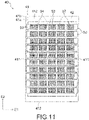
- the frame 41 has a pair of first sides 411 and a pair of second sides 412.
- the frame 41 may have a rectangular contour.
- the masks 50 to which a tensile force is applied may be fixed to the first sides 411.
- the first sides 411 may be longer than the second sides 412.
- the pair of the first sides 411 and the pair of the second sides 412 may surround the opening 42.
- a method of measuring the thickness T of the mask 50 may be a contact measurement method.
- a length gauge HEIDENHAIN-METRO "MT1271" including a ball bush guide plunger, which is manufactured by HEIDENHAIN, may be used.
- the alignment marks 50M of the masks 50A to 50C may overlap.
- the masks 50A to 50C may be stacked based on the arrangement of the cells 52 of the masks 50A to 50C.
- the masks 50A to 50C may be stacked based on the arrangement of the through-holes 53A to 53C and the shield regions 54A to 54C of the masks 50A to 50C.
- a tensile force may be applied to the masks 50A to 50C, or a tensile force may not be applied thereto.
Landscapes
- Chemical & Material Sciences (AREA)
- Engineering & Computer Science (AREA)
- Physics & Mathematics (AREA)
- Optics & Photonics (AREA)
- Manufacturing & Machinery (AREA)
- Mechanical Engineering (AREA)
- Chemical Kinetics & Catalysis (AREA)
- Materials Engineering (AREA)
- Metallurgy (AREA)
- Organic Chemistry (AREA)
- Inorganic Chemistry (AREA)
- Geometry (AREA)
- Microelectronics & Electronic Packaging (AREA)
- Life Sciences & Earth Sciences (AREA)
- Sustainable Development (AREA)
- Electroluminescent Light Sources (AREA)
- Physical Vapour Deposition (AREA)
Abstract
Description
- An embodiment of the present disclosure relates to a mask group, a method of manufacturing an organic device, and an organic device.
- For electronic devices such as smart phones and tablet PCs, there has been a need for high-definition display devices in markets. A display device has a pixel density of, for example, 400 ppi or more or 800 ppi or more.
- An organic electroluminescent display device attracts attention because of excellent responsiveness and/or low power consumption. A known method of forming pixels of the organic electroluminescent display device is to attach the material of the pixels to a substrate by deposition. For example, a substrate on which an anode is formed in a pattern suitable for an element is first prepared. Subsequently, an organic material is attached to the anode via a through-hole in a mask, and an organic layer is formed on the anode. Subsequently, a conductive material is attached to the organic layer via the through-hole of the mask, and a cathode is formed on the organic layer.
- In some cases, the cathode is formed by using a deposition method in which multiple masks are used. In these cases, layers that are included in the cathode are formed by the masks, and adjacent layers overlap in an electrode overlapping region. Consequently, the layers are electrically connected to each other.
- Patent Document 1:
JP 2019-060028 A - Patent Document 2:
JP 2005-183153 A - As the thickness of the electrode overlapping region of the cathode increases, optical transmittance decreases.
- A mask group according to an embodiment of the present disclosure may include two or more masks. The mask may include a shield region and a through-hole. A mask multilayer body in which the two or more masks are stacked may have a penetration region that overlaps the through-hole when viewed in a normal direction of the masks. The mask multilayer body may have a first mask region that contains the penetration region that has a first aperture ratio and a second mask region that contains the penetration region that has a second aperture ratio lower than the first aperture ratio when viewed in the normal direction of the masks. The masks may have a first surface and a second surface that is located opposite the first surface. The through-hole may include a first recessed portion that is located at the first surface, a second recessed portion that is located at the second surface, and a connection portion at which the first recessed portion and the second recessed portion are connected to each other. When a section in the normal direction is viewed, a region-defining straight line may be defined as a straight line that passes through the connection portion and that forms an angle θ together with the first surface, the region-defining straight line may intersect the first surface at a first intersection point, an effective region may be defined as a region inside the first intersection point in the through-hole, and a peripheral region may be defined as a region outside the first intersection point in the through-hole. The angle θ may be 35° or more and 70° or less. The penetration region in the second mask region may include a hole overlapping region in which the through-holes of the two masks overlap. The hole overlapping region may include a first hole overlapping region in which the peripheral regions of the through-holes of the two masks that are included in the mask multilayer body overlap.
- According to an embodiment of the present disclosure, optical transmittance can be increased.
-
-
Fig. 1 is a plan view of an example of an organic device according to an embodiment of the present disclosure. -
Fig. 2 is a plan view of a second display region of the organic device. -
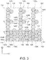
Fig. 3 is a plan view of second electrode of the organic device. -
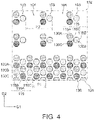
Fig. 4 is a plan view of the organic device illustrated inFig. 3 with the second electrode removed therefrom. -
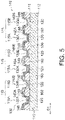
Fig. 5 is a sectional view of the organic device illustrated inFig. 3 substantially taken along line A-A. -
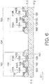
Fig. 6 is a sectional view of the organic device illustrated inFig. 3 substantially taken along line B-B. -
Fig. 7 is a plan view of electrode overlapping regions of the second electrode illustrated inFig. 3 . -
Fig. 8 is a sectional view of the electrode overlapping regions illustrated inFig. 7 . -
Fig. 9 is a sectional view of a comparative example of the electrode overlapping regions. -
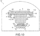
Fig. 10 illustrates an example of a deposition apparatus that includes a mask apparatus. -
Fig. 11 is a plan view of an example of the mask apparatus. -
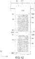
Fig. 12 is a plan view of a mask of the mask apparatus. -
Fig. 13A is a plan view of a first mask apparatus. -
Fig. 13B is a plan view of a second mask apparatus. -
Fig. 13C illustrates a third mask apparatus. -
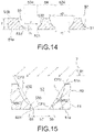
Fig. 14 is a sectional view of an example of a mask sectional structure. -
Fig. 15 is a sectional view of an effective region and a peripheral region of a through-hole. -
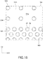
Fig. 16 is a plan view of an example of a first mask for forming the second electrode illustrated inFig. 3 . -
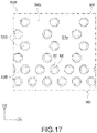
Fig. 17 is a plan view of an example of a second mask for forming the second electrode illustrated inFig. 3 . -
Fig. 18 is a plan view of an example of a third mask for forming the second electrode illustrated inFig. 3 . -
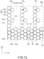
Fig. 19 is a plan view of an example of a mask multilayer body for forming the second electrode illustrated inFig. 3 . -
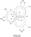
Fig. 20 is a plan view of hole overlapping regions of the mask multilayer body illustrated inFig. 19 . -
Fig. 21 is a sectional view of the hole overlapping regions illustrated inFig. 20 . -
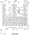
Fig. 22 is a plan view of a modification to the second electrode illustrated inFig. 3 . -
Fig. 23 is a plan view of the electrode overlapping regions of the second electrode illustrated inFig. 22 . -
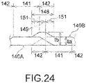
Fig. 24 is a sectional view of the electrode overlapping regions illustrated inFig. 23 . -
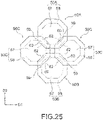
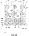
Fig. 25 is a plan view of the hole overlapping regions of the mask multilayer body for forming the second electrode illustrated inFig. 22 . -
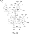
Fig. 26 is a sectional view of the hole overlapping regions illustrated inFig. 25 . -
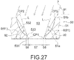
Fig. 27 is a sectional view of a modification to the effective region and the peripheral region of the through-hole illustrated inFig. 15 . -
Fig. 28 is a plan view of a modification to the second electrode illustrated inFig. 3 . -
Fig. 29 is a plan view of the electrode overlapping regions of the second electrode illustrated inFig. 28 . -
Fig. 30 is a plan view of an example of the first mask for forming the second electrode illustrated inFig. 28 . -
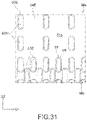
Fig. 31 is a plan view of an example of the second mask for forming the second electrode illustrated inFig. 28 . -
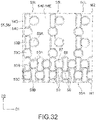
Fig. 32 is a plan view of the hole overlapping regions of the mask multilayer body for forming the second electrode illustrated inFig. 28 . -
Fig. 33 is a plan view of the hole overlapping regions of the mask multilayer body illustrated inFig. 32 . - In the present specification and the drawings, words that mean substances on which components such as a "substrate", a "base material", a "plate", a "sheet", and a "film" are based are not distinguished from each other only based on different names unless there is a particular description.
- In the present specification and the drawings, words such as "parallel" and "perpendicular" and the values of a length and an angle that specify shapes, geometrical conditions, and the degree of these, for example, are not limited by strict meaning but are interpreted to an extent that the same function can be expected unless there is a particular description.
- In some cases where a component such as a member or a region is "on" or "under", "on an upper side of" or "on a lower side of", or "above" or "below" another component such as another member or another region in the present specification and the drawings, the cases include a case where the component is in direct contact with the other component unless there is a particular description. The cases also include a case where another component is between the component and the other component, that is, a case where the component and the other component are indirectly connected to each other. As for the words "on", "upper side", and "above", or "under", "lower side", and "below", an up-down direction may be reversed unless there is a particular description.
- In the present specification and the drawings, like portions or portions that have the same function are designated by like reference characters or similar reference characters unless there is a particular description, and a duplicated description for these is omitted in some cases. For convenience of description, the ratio of dimensions in the drawings differs from an actual ratio, and an illustration of a part of a component is omitted in the drawings in some cases.
- In the present specification and the drawings, an embodiment of the present disclosure may be combined with another embodiment or a modification without contradiction unless there is a particular description. Other embodiments may be combined with each other, and another embodiment and a modification may be combined with each other without contradiction. Modifications may be combined with each other without contradiction.
- In the case where multiple processes related to a method such as a manufacturing method are disclosed in the present specification and the drawings, another process that is not disclosed may be performed between the disclosed processes unless there is a particular description. The order of the disclosed processes is freely selected without contradiction.
- In the present specification and the drawings, a range that is represented by the character "to" includes numerals or factors placed in front of and behind the character "to" unless there is a particular description. For example, the numerical range that is defined by the expression "34 to 38 mass%" is the same as the numerical range that is defined by the expression "34 mass% or more and 38 mass% or less". For example, the range that is defined by the expression "masks 50A to 50C" includes
masks - According to an embodiment of the present specification, an example of the use of a mask group that includes multiple masks to form an electrode on a substrate when an organic electroluminescent display device is manufactured will be described. However, the use of the mask group is not particularly limited. The present embodiment can be used for mask groups that are used in various ways. For example, the mask group according to the present embodiment may be used to form an electrode of a device that displays or projects an image or a picture for creating virtual reality, that is, VR or augmented reality, that is, AR. The mask group according to the present embodiment may be used to form an electrode of a display device other than an organic electroluminescent display device such as an electrode of a liquid-crystal display device. The mask group according to the present embodiment may be used to form an electrode of an organic device other than a display device such as an electrode of a pressure sensor.
- According to a first aspect of the present disclosure, a mask group includes two or more masks. The mask includes a shield region and a through-hole. A mask multilayer body in which the two or more masks are stacked has a penetration region that overlaps the through-hole when viewed in a normal direction of the mask. The mask multilayer body has a first mask region that contains the penetration region that has a first aperture ratio and a second mask region that contains the penetration region that has a second aperture ratio lower than the first aperture ratio when viewed in the normal direction of the mask. The mask has a first surface and a second surface that is located opposite the first surface. The through-hole includes a first recessed portion that is located at the first surface, a second recessed portion that is located at the second surface, and a connection portion at which the first recessed portion and the second recessed portion are connected to each other. When a section in the normal direction is viewed, a region-defining straight line is defined as a straight line that passes through the connection portion and that forms an angle θ together with the first surface, the region-defining straight line intersects the first surface at a first intersection point, an effective region is defined as a region inside the first intersection point in the through-hole, and a peripheral region is defined as a region outside the first intersection point in the through-hole. The angle θ is 35° or more and 70° or less. The penetration region in the second mask region includes a hole overlapping region in which the through-holes of the two masks overlap. The hole overlapping region includes a first hole overlapping region in which the peripheral regions of the through-holes of the two masks that are included in the mask multilayer body overlap.
- According to a second aspect of the present disclosure, in the mask group according to the first aspect described above, the first hole overlapping region may be separated from the effective region of the through-holes of the mask.
- According to a third aspect of the present disclosure, in the mask group according to the first aspect described above, the hole overlapping region may include a second hole overlapping region in which the effective region of the through-hole of one of the masks that are included in the mask multilayer body and the peripheral region of the through-hole of another of the masks overlap.
- According to a fourth aspect of the present disclosure, in the mask group according to any one of the first aspect described above to the third aspect described above, the region-defining straight line may be in contact with a freely selected point on a wall surface of the second recessed portion.
- According to a fifth aspect of the present disclosure, in the mask group according to any one of the first aspect described above to the fourth aspect described above, the two or more masks may include a plurality of the through-holes in the first mask region and the second mask region.
- According the sixth aspect of the present disclosure, a method of manufacturing an organic device may include a second electrode formation step of forming a second electrode on an organic layer on a first electrode on a substrate by using the mask group according to any one of the first aspect described above to the fifth aspect described above. The second electrode formation step may include forming a first layer of the second electrode by using a deposition method in which one of the masks is used and forming a second layer of the second electrode by using a deposition method in which another of the masks is used.
- According to a seventh aspect of the present disclosure, in the method according to the sixth aspect described above, an angle θ of the region-defining straight line may be equal to an angle θ1. θ1 may be an angle that is formed between the first surfaces of the mask and a coming direction in which a deposition material for forming the second electrode comes. θ2 may be an angle that is formed between the first surfaces and a straight line that passes through the connection portion and that is in contact with the second recessed portion. The angle θ1 is larger than the angle θ2.
- According to an eighth aspect of the present disclosure, an organic device includes a substrate, a first electrode that is located on the substrate, organic layers that are located on the first electrode, and a second electrode that is located on the organic layers. The organic device has a first display region that contains the second electrode that has a first occupancy ratio and a second display region that contains the second electrode that has a second occupancy ratio lower than the first occupancy ratio when viewed in a normal direction of the substrate. The second electrode includes two or more layers that are located on the organic layers that differ from each other. The layer has a main layer region and a peripheral layer region thinner than the main layer region. The second electrode in the second display region has an electrode overlapping region in which the two layers overlap. The electrode overlapping region includes a first electrode overlapping region in which the peripheral layer regions of the layers overlap and a second electrode overlapping region in which the main layer region of one of the layers and the peripheral layer region of another of the layers overlap.
- An embodiment of the present disclosure will be described in detail with reference to the drawings. The embodiment described below is an example of an embodiment of the present disclosure, and the present disclosure is not interpreted so as to be limited to only the embodiment.
- An
organic device 100 will be described. Theorganic device 100 includes an electrode that is formed by using a mask group according to the present embodiment.Fig. 1 is a plan view of an example of theorganic device 100 viewed in the normal direction of asubstrate 110 of theorganic device 100. In the following description, viewing a surface of a substance on which the substrate, for example, is based in the normal direction is also referred to as "in a plan view". - The
organic device 100 includes the substrate 110 (seeFig. 5 ) andmultiple elements 115 that are arranged on afirst surface 111 or asecond surface 112 of thesubstrate 110. For example, theelements 115 are pixels. As illustrated inFig. 1 , theorganic device 100 may have afirst display region 101 and asecond display region 102 in a plan view. Thesecond display region 102 may have an area smaller than that of thefirst display region 101. As illustrated inFig. 1 , thesecond display region 102 may be surrounded by thefirst display region 101. A part of an outer edge of thesecond display region 102 may be located on the same straight line as a part of an outer edge of thefirst display region 101 although this is not illustrated. -
Fig. 2 is an enlarged plan view of thesecond display region 102 and the vicinity thereof inFig. 1 . In thefirst display region 101, theelements 115 may be arranged in two different directions. In an example illustrated inFig. 1 andFig. 2 , two ormore elements 115 in thefirst display region 101 may be arranged in a first element direction G1. Two ormore elements 115 in thefirst display region 101 may be arranged in a second element direction G2 that intersects the first element direction G1. The second element direction G2 may be perpendicular to the first element direction G1. - The
organic device 100 includes asecond electrode 140. Thesecond electrode 140 is located onorganic layers 130 described later. Thesecond electrode 140 may be electrically connected to two or moreorganic layers 130. For example, thesecond electrode 140 may overlap the two or moreorganic layers 130 in a plan view. Thesecond electrode 140 that is located in thefirst display region 101 is also referred to assecond electrode 140X. Thesecond electrode 140 that is located in thesecond display region 102 is also referred to assecond electrode 140Y. - The
second electrode 140X has a first occupancy ratio. The first occupancy ratio is calculated by dividing the sum of the areas of thesecond electrode 140 that is located in thefirst display region 101 by the area of thefirst display region 101. Thesecond electrode 140Y has a second occupancy ratio. The second occupancy ratio is calculated by dividing the sum of the areas of thesecond electrode 140 that is located in thesecond display region 102 by the area of thesecond display region 102. The second occupancy ratio may be lower than the first occupancy ratio. For example, as illustrated inFig. 2 , thesecond display region 102 may includenon-transparent regions 103 andtransparent regions 104. Thetransparent region 104 do not overlap thesecond electrode 140Y in a plan view. Thenon-transparent region 103 overlap thesecond electrode 140Y in a plan view. - The first occupancy ratio may be higher than 0% and lower than 100%. In this case, the
first display region 101 includes a region that is occupied by any offirst layers 140A tothird layers 140C of thesecond electrode 140 described later and a region that is occupied by none of thefirst layers 140A to thethird layers 140C. However, the present disclosure is not limited thereto. The first occupancy ratio may be 100%. In this case, the entirefirst display region 101 is occupied by any of thefirst layers 140A to thethird layers 140C of thesecond electrode 140. The second occupancy ratio may be higher than 0% and lower than 100%. In this case, thesecond display region 102 includes a region that is occupied by any of thefirst layers 140A to thethird layers 140C of thesecond electrode 140 and a region that is occupied by none of thefirst layers 140A to thethird layers 140C. - For example, the ratio of the second occupancy ratio to the first occupancy ratio may be 0.2 or more, may be 0.3 or more, or may be 0.4 or more. For example, the ratio of the second occupancy ratio to the first occupancy ratio may be 0.6 or less, may be 0.7 or less, or may be 0.8 or less. The range of the ratio of the second occupancy ratio to the first occupancy ratio may be determined by using a first group consisting of 0.2, 0.3, and 0.4 and/or a second group consisting of 0.6, 0.7, and 0.8. The range of the ratio of the second occupancy ratio to the first occupancy ratio may be determined by using a combination of a value freely selected from the values in the first group described above and a value freely selected from the values in the second group described above. The range of the ratio of the second occupancy ratio to the first occupancy ratio may be determined by using a combination of two values freely selected from the values in the first group described above. The range of the ratio of the second occupancy ratio to the first occupancy ratio may be determined by using a combination of two values freely selected from the values in the second group described above. For example, the range may be 0.2 or more and 0.8 or less, may be 0.2 or more and 0.7 or less, may be 0.2 or more and 0.6 or less, may be 0.2 or more and 0.4 or less, may be 0.2 or more and 0.3 or less, may be 0.3 or more and 0.8 or less, may be 0.3 or more and 0.7 or less, may be 0.3 or more and 0.6 or less, may be 0.3 or more and 0.4 or less, may be 0.4 or more and 0.8 or less, may be 0.4 or more and 0.7 or less, may be 0.4 or more and 0.6 or less, may be 0.6 or more and 0.8 or less, may be 0.6 or more and 0.7 or less, or may be 0.7 or more and 0.8 or less.
- The transmittance of the
non-transparent region 103 is also referred to as a first transmittance. The transmittance of thetransparent region 104 is also referred to as a second transmittance. Thetransparent region 104 do not contain thesecond electrode 140Y, and accordingly, the second transmittance is higher than the first transmittance. For this reason, in thesecond display region 102 including thetransparent regions 104, light that reaches theorganic device 100 passes through thetransparent region 104 and can reach, for example, an optical component at the back of thesubstrate 110. An example of the optical component is a component that detects light to perform a function such as a camera. Thesecond display region 102 includes thenon-transparent regions 103, and accordingly, a picture can be displayed in thesecond display region 102 in the case where theelements 115 are pixels. Thesecond display region 102 can thus detect light and display a picture. Examples of the function of thesecond display region 102 that is performed by detecting light include those of a camera and a sensor such as a fingerprint sensor or a face recognition sensor. The amount of light that is received by the sensor can be increased by increasing the second transmittance of thetransparent region 104. The amount of light that is received by the sensor can be increased by decreasing the second occupancy ratio of thesecond display region 102. - In the case where any one of the dimensions of the
non-transparent regions 103 in the first element direction G1 and in the second element direction G2 and the dimensions of thetransparent regions 104 in the first element direction G1 and in the second element direction G2 is 1 mm or less, the first transmittance and the second transmittance may be measured by using a microspectrophotometer. OSP-SP200 manufactured by Olympus Corporation or any one of LCF series manufactured by Otsuka Electronics Co., Ltd., may be used as the microspectrophotometer. These microspectrophotometers can measure transmittance in a visible range of 380 nm or more and 780 nm or less. Quartz, borosilicate glass for TFT liquid crystal, or alkali glass for TFT liquid crystal may be used as reference. The result of measurement at 550 nm may be used as the first transmittance and the second transmittance. - In the case where any one of the dimensions of the
non-transparent regions 103 in the first element direction G1 and in the second element direction G2 and the dimensions of thetransparent regions 104 in the first element direction G1 and in the second element direction G2 is more than 1 mm, the first transmittance and the second transmittance may be measured by using a spectrophotometer. Ultraviolet visible light spectrophotometer UV-2600i or UV-3600i Plus manufactured by SHIMADZU CORPORATION may be used as the spectrophotometer. A fine luminous flux diaphragm unit is mounted on the spectrophotometer. This enables the transmittance of a region that has a dimension of 1 mm at the maximum to be measured. The atmosphere may be used as reference. The result of measurement at 550 nm may be used as the first transmittance and the second transmittance. - For example, a ratio TR2/TR1 of a second transmittance TR2 to a first transmittance TR1 may be 1.2 or more, may be 1.5 or more, or may be 1.8 or more. For example, the TR2/TR1 may be 2 or less, may be 3 or less, or may be 4 or less. The range of the TR2/TR1 may be determined by using a first group consisting of 1.2, 1.5, and 1.8 and/or a second group consisting of 2, 3, and 4. The range of the TR2/TR1 may be determined by using a combination of a value freely selected from the values in the first group described above and a value freely selected from the values in the second group described above. The range of the TR2/TR1 may be determined by using a combination of two values freely selected from the values in the first group described above. The range of the TR2/TR1 may be determined by using a combination of two values freely selected from the values in the second group described above. For example, the range may be 1.2 or more and 4 or less, may be 1.2 or more and 3 or less, may be 1.2 or more and 2 or less, may be 1.2 or more and 1.8 or less, may be 1.2 or more and 1.5 or less, may be 1.5 or more and 4 or less, may be 1.5 or more and 3 or less, may be 1.5 or more and 2 or less, may be 1.5 or more and 1.8 or less, may be 1.8 or more and 4 or less, may be 1.8 or more and 3 or less, may be 1.8 or more and 2 or less, may be 2 or more and 4 or less, may be 2 or more and 3 or less, or may be 3 or more and 4 or less.
- As illustrated in
Fig. 2 , thesecond electrode 140Y may include two ormore electrode lines 140L that are arranged in the first element direction G1. The electrode lines 140L may extend in the second element direction G2. For example, theelectrode line 140L may have first end 140L1 and second end 140L2 that are connected to thesecond electrode 140X in thefirst display region 101. The second end 140L2 is located opposite the first end 140L1 in the second element direction G2. In the case where a part of the outer edge of thesecond display region 102 is located on the same straight line as a part of the outer edge of thefirst display region 101 although this is not illustrated, only one of the ends of theelectrode line 140L may be connected to thesecond electrode 140X. -
Fig. 3 is an enlarged plan view of thesecond electrode 140X in thefirst display region 101 and thesecond electrode 140Y in thesecond display region 102. Thesecond electrode 140X and thesecond electrode 140Y may overlap theorganic layers 130 in a plan view. Theorganic layers 130 are components of theelements 115. - In the
first display region 101, theorganic layers 130 may be arranged at a first pitch P1 (seeFig. 4 ) in the first element direction G1. In thesecond display region 102, theorganic layers 130 may be arranged at a second pitch P2 in the first element direction G1. The second pitch P2 may be larger than the first pitch P1. Consequently, the second occupancy ratio of thesecond electrode 140Y decreases. This enables the areas of thetransparent region 104 to increase and enables the amount of light that is received by the sensor to increase. - For example, the ratio of the second pitch P2 to the first pitch P1 may be 1.1 or more, may be 1.3 or more, or may be 1.5 or more. For example, the ratio of the second pitch P2 to the first pitch P1 may be 2.0 or less, may be 3.0 or less, or may be 4.0 or less. The range of the ratio of the second pitch P2 to the first pitch P1 may be determined by using a first group consisting of 1.1, 1.3, and 1.5 and/or a second group consisting of 2.0, 3.0, and 4.0. The range of the ratio of the second pitch P2 to the first pitch P1 may be determined by using a combination of a value freely selected from the values in the first group described above and a value freely selected from the values in the second group described above. The range of the ratio of the second pitch P2 to the first pitch P1 may be determined by using a combination of two values freely selected from the values in the first group described above. The range of the ratio of the second pitch P2 to the first pitch P1 may be determined by using a combination of two values freely selected from the values in the second group described above. For example, the range may be 1.1 or more and 4.0 or less, may be 1.1 or more and 3.0 or less, may be 1.1 or more and 2.0 or less, may be 1.1 or more and 1.5 or less, may be 1.1 or more and 1.3 or less, may be 1.3 or more and 4.0 or less, may be 1.3 or more and 3.0 or less, may be 1.3 or more and 2.0 or less, may be 1.3 or more and 1.5 or less, may be 1.5 or more and 4.0 or less, may be 1.5 or more and 3.0 or less, may be 1.5 or more and 2.0 or less, may be 2.0 or more and 4.0 or less, may be 2.0 or more and 3.0 or less, or may be 3.0 or more and 4.0 or less. In the case where the ratio of the second pitch P2 to the first pitch P1 is small, a difference between the pixel density of the
first display region 101 and the pixel density of thesecond display region 102 is small. This inhibits a visual difference between thefirst display region 101 and thesecond display region 102 from being made. - The
electrode line 140L may overlap the two or moreorganic layers 130 that are arranged in the second element direction G2 in a plan view. - Layered structures of the
second electrode 140 will be described. - The
second electrode 140 may include multiple layers. For example, thesecond electrode 140 may include thefirst layers 140A, thesecond layers 140B, and thethird layers 140C. The first layers 140A, thesecond layers 140B, and thethird layers 140C are formed by using a deposition method. More specifically, thefirst layers 140A are formed by using the deposition method in which afirst mask 50A is used. The second layers 140B are formed by using the deposition method in which asecond mask 50B is used. The third layers 140C are formed by using the deposition method in which athird mask 50C is used. - As illustrated in
Fig. 7 and Fig. 8 , each of thelayers 140A to 140C of thesecond electrode 140 hasmain layer region 141 andperipheral layer region 142. - The
main layer region 141 is located at the centers of the layer in a plan view and are unlikely to be affected by shadow described later. Themain layer region 141 is thicker than theperipheral layer region 142. Themain layer region 141 may be relatively flat. Themain layer region 141 may be defined byeffective region 57 of through-hole 53 described later. - The
peripheral layer region 142 is located outside themain layer region 141 and around themain layer region 141. Theperipheral layer region 142 is likely to be affected by the shadow. Theperipheral layer region 142 is thinner than themain layer region 141. The thickness of theperipheral layer region 142 may vary. Theperipheral layer region 142 may be defined byperipheral region 58 of the through-hole 53 described later. - The
peripheral layer region 142 may have a thickness of 95% or less of the thickness ta of themain layer region 141. That is, the thickness of theperipheral layer region 142 may change within a range of 95% or less of the thickness ta of themain layer region 141. For example, the percentage of the thickness to the thickness ta may be 80% or less or 50% or less. - The
layers 140A to 140C of thesecond electrode 140 may have a contour that has a substantially polygonal shape in a plan view or a contour that has a substantially circular shape. For example, the layers may have a contour that has a substantially quadrilateral shape, a substantially hexagonal shape, or a substantially octagonal shape. In an example illustrated inFig. 3 , thelayers 140A to 140C have a contour that has a substantially regular octagonal shape. Thelayers 140A to 140C may have the same planar contour. Two sides that face each other extend in the first element direction G1. Other two sides that face each other extend in the second element direction G2. In the case where thelayers 140A to 140C have a contour that has a substantially polygonal shape, four corners of the contour may be curved. - The
first layer 140A may be connected to thesecond layer 140B and thethird layer 140C in the first element direction G1 and in the second element direction G2. Thefirst layer 140A may overlap theorganic layer 130 in a plan view. For example, thefirst layer 140A may overlap firstorganic layer 130A described later. Thefirst layer 140A may be located on theorganic layer 130 that differ from those on which thesecond layer 140B and thethird layer 140C are located. - The
second layer 140B may be connected to thefirst layer 140A and thethird layer 140C in the first element direction G1 and in the second element direction G2. Thesecond layer 140B may overlap theorganic layer 130 in a plan view. For example, thesecond layer 140B may overlap secondorganic layer 130B described later. Thesecond layer 140B may be located on theorganic layer 130 that differ from those on which thefirst layer 140A and thethird layer 140C are located. - The
third layer 140C may be connected to thefirst layer 140A and thesecond layer 140B in the first element direction G1 and in the second element direction G2. Thethird layer 140C may overlap theorganic layer 130 in a plan view. For example, thethird layer 140C may overlap thirdorganic layer 130C described later. Thethird layer 140C may be located on theorganic layer 130 that differ from those on which thefirst layer 140A and thesecond layer 140B are located. - In the
first display region 101, thefirst layers 140A, thesecond layers 140B, and thethird layers 140C may be continuously arranged in the first element direction G1 and in the second element direction G2. In the example illustrated inFig. 3 , thefirst layer 140A, thesecond layer 140B, and thethird layer 140C are located on vertices of an equilateral triangle. A single pixel is configured by threelayers first electrode 120 and theorganic layer 130. - In the
second display region 102, thefirst layers 140A, thesecond layers 140B, and thethird layers 140C may be continuously arranged in the first element direction G1 and in the second element direction G2. In the example illustrated inFig. 3 , a single pixel is configured by threelayers first display region 101. The pixels are arranged at an interval in the first element direction G1. Thetransparent region 104 are interposed between the adjacent pixels in the first element direction G1. The pixels are arranged at an interval in the second element direction G2. Thesecond layer 140B is interposed between two adjacent pixels in the second element direction G2. Thefirst electrode 120 and theorganic layer 130 are not associated with thesecond layer 140B, and insulatinglayers 160 are interposed between thesecond layer 140B that are not included in the pixels and thesubstrate 110. The second layers 140B that are not included in the pixels form theelectrode lines 140L and ensure the conductivity of thesecond electrode 140. -
Fig. 4 is a plan view of theorganic device 100 illustrated inFig. 3 with thesecond electrode 140 removed therefrom. Theorganic layer 130 may include the firstorganic layers 130A, the secondorganic layers 130B, and the thirdorganic layers 130C. For example, the firstorganic layer 130A, the secondorganic layer 130B, and the thirdorganic layer 130C are red light-emitting layer, blue light-emitting layer, and green light-emitting layer. In the following description, the words and reference characters of the "organic layer 130" are used in the case where an organic layer structure that is common to the firstorganic layer 130A, the secondorganic layer 130B, and the thirdorganic layer 130C is described. The firstorganic layer 130A, the secondorganic layer 130B, and the thirdorganic layer 130C are located on vertices of an equilateral triangle as in the threelayers 140A to 140C of thesecond electrode 140. - The arrangement of the
second electrode 140 and theorganic layer 130 in a plan view is detected by observing theorganic device 100 by using a digital microscope having high magnification. The occupancy ratios described above, an area, a dimension, a gap can be calculated based on the result of detection. In the case where theorganic device 100 includes a cover such as a glass cover, thesecond electrode 140 and theorganic layer 130 may be observed after the cover is removed. The cover may be removed by being peeled or broken. A scanning electron microscope may be used instead of the digital microscope. - An example of the layered structure of the
organic device 100 will now be described.Fig. 5 is a sectional view of the organic device illustrated inFig. 3 substantially taken along line A-A.Fig. 6 is a sectional view of the organic device illustrated inFig. 3 substantially taken along line B-B. - The
organic device 100 includes thesubstrate 110 and theelements 115 that are located on thesubstrate 110 as described above. Theelement 115 may include thefirst electrode 120, theorganic layer 130 that are located on thefirst electrode 120, and thesecond electrode 140 that are located on theorganic layer 130 as described above. - The
organic device 100 may include the insulatinglayers 160 each of which is located between twofirst electrodes 120 adjacent to each other in a plan view. The insulatinglayer 160 may contain, for example, polyimide. The insulatinglayer 160 may overlap end portions of thefirst electrode 120. - The insulating
layer 160 may overlapelectrode overlapping region 148 described later in a plan view. For example, theelectrode overlapping region 148 may be surrounded by the contours of the insulatinglayer 160 in a plan view. - The
electrode overlapping region 148 contain the multiple layers of thesecond electrode 140. For this reason, theelectrode overlapping region 148 have a transmittance lower than that of a single layer of thesecond electrode 140. In some cases where light that passes through theelectrode overlapping region 148 exits from theorganic device 100, the intensity of the light is non-uniform. The insulatinglayer 160 that overlap theelectrode overlapping region 148 inhibit the intensity of the light from being non-uniform. - In each
electrode overlapping region 148, two layers partly overlap in a plan view. In the example illustrated inFig. 3 , theelectrode overlapping region 148 includes a region in which thefirst layer 140A and thesecond layer 140B overlap, a region in which thefirst layer 140A and thethird layer 140C overlap, and a region in which thesecond layer 140B and thethird layer 140C overlap in a plan view. A region in which threelayers - As illustrated in
Fig. 7 and Fig. 8 , theelectrode overlapping region 148 may include firstelectrode overlapping region 149 in which theperipheral layer regions 142 of the layers overlap.Fig. 7 is a plan view of theelectrode overlapping regions 148.Fig. 8 is a sectional view of theelectrode overlapping regions 148. - For example, the first
electrode overlapping region 149 include a region in which theperipheral layer region 142 of thefirst layer 140A and theperipheral layer region 142 of thesecond layer 140B overlap, a region in which theperipheral layer region 142 of thefirst layer 140A and theperipheral layer region 142 of thethird layer 140C overlap, and a region in which theperipheral layer region 142 of thesecond layer 140B and theperipheral layer region 142 of thethird layer 140C overlap. According to the present embodiment, theelectrode overlapping region 148 include the firstelectrode overlapping region 149 in which theperipheral layer regions 142 of the layers overlap. In the electrode overlapping region, themain layer regions 141 of the layers may not overlap. Themain layer regions 141 of the layers may not overlap. - As illustrated in
Fig. 8 , theperipheral layer regions 142 overlap, and the thickness of thesecond electrode 140 in theelectrode overlapping region 148 can be consequently decreased. For example, in the case where themain layer regions 141 overlap as illustrated inFig. 9 , the maximum thickness tb of thesecond electrode 140 in theelectrode overlapping region 148 is twice the thickness ta of themain layer region 141. In the case where theperipheral layer regions 142 overlap, however, the thickness tb of thesecond electrode 140 in theelectrode overlapping region 148 is less than twice the thickness ta of themain layer region 141. For this reason, themain layer regions 141 do not overlap, and the thickness tb of thesecond electrode 140 in theelectrode overlapping region 148 can be decreased. - As illustrated in
Fig. 8 , the firstelectrode overlapping region 149 may be separated from themain layer region 141.Non-overlapping region 150 may be located between the firstelectrode overlapping region 149 and themain layer region 141. - For example, the first
electrode overlapping region 149 in which theperipheral layer region 142 of thefirst layer 140A and theperipheral layer region 142 of thesecond layer 140B overlap may be separated from themain layer region 141 of thefirst layer 140A. Thenon-overlapping region 150 may be located between the firstelectrode overlapping region 149 and themain layer region 141 of thefirst layer 140A. The firstelectrode overlapping region 149 in which theperipheral layer region 142 of thefirst layer 140A and theperipheral layer region 142 of thesecond layer 140B overlap may be separated from themain layer region 141 of thesecond layer 140B. Thenon-overlapping region 150 may be located between the firstelectrode overlapping region 149 and themain layer region 141 of thesecond layer 140B. - Similarly, the first
electrode overlapping region 149 in which theperipheral layer region 142 of thefirst layer 140A and theperipheral layer region 142 of thethird layer 140C overlap may be separated from themain layer regions 141 of thelayers - Similarly, the first
electrode overlapping region 149 in which theperipheral layer region 142 of thesecond layer 140B and theperipheral layer region 142 of thethird layer 140C overlap may be separated from themain layer regions 141 of thelayers - The
organic device 100 may be an active-matrix device. For example, theorganic device 100 may include switches although this is not illustrated. The switches are electrically connected to the respectivemultiple elements 115. Examples of the switches may include transistors. The switches can control on-off of a voltage or current to therespective elements 115. - The
substrate 110 has thefirst surface 111 and thesecond surface 112. Thesubstrate 110 may be an insulating plate member. Thesubstrate 110 preferably has transparency and allow light to pass therethrough. - In the case where the
substrate 110 has predetermined optical transparency, the degree of the transparency of thesubstrate 110 may be such that light from theorganic layers 130 can pass therethrough and can be displayed. For example, the transmittance of thesubstrate 110 in a visible-light region may be 70% or more or may be 80% or more. The transmittance of thesubstrate 110 may be measured by using a test method for Plastics-Determination of the total luminous transmittance of transparent materials based on JIS K7361-1. - The
substrate 110 may be flexible or may not be flexible. The material of thesubstrate 110 may be appropriately selected depending on the use of theorganic device 100. - Examples of the material of the
substrate 110 may include inflexible rigid materials such as quartz glass, Pyrex (registered trademark) glass, a synthetic quartz plate, and non-alkali glass and flexible materials such as resin film, an optical resin plate, and thin glass. The substrate may have a multilayer body that includes a barrier layer on a surface of the resin film or barrier layers on surfaces of the resin film. - The thickness of the
substrate 110 may be appropriately selected depending on, for example, the material used for thesubstrate 110 or the use of theorganic device 100. For example, the thickness of thesubstrate 110 may be 0.005 mm or more. The thickness of thesubstrate 110 may be 5 mm or less. - The
elements 115 may perform a function in a manner in which a voltage is applied between thefirst electrode 120 and thesecond electrode 140 or a current flows between thefirst electrode 120 and thesecond electrode 140. For example, in the case where theelements 115 are pixels of an organic electroluminescent display device, theelements 115 can emit light for forming a picture. - The
first electrode 120 contain a conductive material. For example, thefirst electrode 120 may contain metal, a conductive metal oxide or another conductive inorganic material. Thefirst electrode 120 may contain a conductive metal oxide that has transparency such as an indium tin oxide. - The material of the
first electrodes 120 may be metal such as Au, Cr, Mo, Ag, or Mg, an indium tin oxide abbreviated as ITO, an indium zinc oxide abbreviated as IZO, a zinc oxide, an inorganic oxide such as indium oxide, or a conductive polymer such as polythiophene doped with metal. These conductive materials may be used alone, or two or more kinds of the materials may be combined and used. In the case where two or more kinds of the materials are used, layers composed of the respective materials may be stacked. An alloy containing two or more kinds of the materials may be used. For example, a magnesium alloy such as MgAg may be used. - The
organic layer 130 contain an organic material. When theorganic layer 130 are energized, theorganic layer 130 can perform a function. The phrase "to be energized" means that a voltage is applied to theorganic layer 130, or a current flows through theorganic layer 130. Examples of theorganic layer 130 may include light-emitting layers that emit light when being energized and layers the refractive index or the optical transmittance of which changes when being energized. Theorganic layer 130 may contain an organic semiconductor material. - Multilayer structure that includes the
first electrode 120, the firstorganic layer 130A and thesecond electrode 140 are also referred to asfirst element 115A. Multilayer structure that includes thefirst electrode 120, the secondorganic layer 130B, and thesecond electrode 140 are also referred to assecond element 115B. A multilayer structure that includes thefirst electrode 120, the thirdorganic layer 130C, and thesecond electrode 140 is also referred to asthird element 115C. In the case where theorganic device 100 is an organic electroluminescent display device, thefirst element 115A, thesecond element 115B, and thethird element 115C are sub-pixels. A single pixel may correspond to a combination of thefirst element 115A, thesecond element 115B, and thethird element 115C. - In the following description, the words and reference characters of the "
elements 115" are used in the case where an element structure that is common to thefirst element 115A, thesecond element 115B, and thethird element 115C is described. - When a voltage is applied between the
first electrode 120 and thesecond electrode 140, theorganic layer 130 that are located therebetween are driven. In the case where theorganic layer 130 are light-emitting layer, light is emitted from theorganic layer 130, and the light exits from thesecond electrode 140 to the outside or thefirst electrode 120 to the outside. - In the case where the
organic layer 130 includes light-emitting layer that emit light when being energized, theorganic layer 130 may include a hole injection layer, a hole transport layer, an electron transport layer, an electron injection layer, and another layer. - For example, in the case where the
first electrode 120 are anodes, theorganic layer 130 may include hole injection transport layer between the light-emitting layer and thefirst electrode 120. The hole injection transport layer may be hole injection layer that have a hole injection function, may be hole transport layer that have a hole transport function, or may have both of the hole injection function and the hole transport function. The hole injection layer and the hole transport layer may be stacked on the hole injection transport layer. - In the case where the
second electrode 140 is cathodes, theorganic layer 130 may include electron injection transport layer between the light-emitting layer and thesecond electrode 140. The electron injection transport layer may be electron injection layer that have an electron injection function, may be electron transport layer that have an electron transport function, or may have both of the electron injection function and the electron transport function. The electron injection layer and the electron transport layer may be stacked on the electron injection transport layer. - The light-emitting layer contain a light-emitting material. The light-emitting layer may contain an additive that improves leveling properties.
- A known material may be used as the light-emitting material. Examples of the light-emitting material include a pigment material, a metal complex material, and a polymeric material.
- Examples of the pigment material may include a cyclopentadiene derivative, a tetraphenyl butadiene derivative, a triphenylamine derivative, an oxadiazole derivative, a pyrazoloquinoline derivative, a distyrylbenzene derivative, a distyrylarylene derivative, a silole derivative, a thiophene ring compound, a pyridine ring compound, a perinone derivative, a perylene derivative, an oligothiophene derivative, an oxadiazole dimer, and a pyrazoline dimer.
- Examples of the metal complex material may include a metal complex that includes central metal such as Al, Zn, or Be, or rare-earth metal such as Tb, Eu, or Dy and a ligand such as an oxadiazole, thiadiazole, phenylpyridine, phenylbenzimidazole, or quinoline structure, such as an aluminum quinolinol complex, a benzoquinolinol beryllium complex, a benzoxazole zinc complex, a benzothiazole zinc complex, an azomethyl zinc complex, a porphyrin zinc complex, and a europium complex.
- Examples of the polymeric material may include a poly(p-phenylene vinylene) derivative, a polythiophene derivative, a poly(p-phenylene) derivative, a polysilane derivative, a polyacetylene derivative, a polyvinylcarbazole derivative, a polyfluorene derivative, a polyquinoxaline derivative, and a copolymer thereof.
- The light-emitting layers may contain a dopant in order to improve luminous efficacy or change a luminous wavelength. Examples of the dopant may include a perylene derivative, a coumarin derivative, a rubrene derivative, a quinacridone derivative, a squarylium derivative, a porphyrin derivative, a styryl pigment, a tetracene derivative, a pyrazoline derivative, decacyclene, phenoxazone, a quinoxaline derivative, a carbazole derivative, and a fluorene derivative. Heavy metal ions such as platinum or iridium ions may be contained as the dopant. An organic metal complex that has phosphorescence may be used. A single kind of a dopant may be used, or two or more kinds of dopants may be used.
- For example, materials disclosed in [0125] to [0126] in
JP 2010-272891 A WO 2012/132126 A may be used as the light-emitting material and the dopant. - The thickness of the light-emitting layer are not particularly limited provided that a luminous function can be performed by enabling an electron and a hole to be recombined. For example, the thickness of the light-emitting layer may be 1 nm or more and 500 nm or less.
- A hole injection transport material that is used for the hole injection transport layer may be a known material. Examples of the hole injection transport material may include a triazole derivative, an oxadiazole derivative, an imidazole derivative, a polyaryl alkane derivative, a pyrazoline derivative, a pyrazolone derivative, a phenylenediamine derivative, an arylamine derivative, an amino-substituted chalcone derivative, an oxazole derivative, a styrylanthracene derivative, a fluorenone derivative, a hydrazone derivative, a stilbene derivative, a silazane derivative, a polythiophene derivative, a polyaniline derivative, a polypyrrole derivative, a phenylamine derivative, an anthracene derivative, a carbazole derivative, a fluorene derivative, a distyrylbenzene derivative, a polyphenylene vinylene derivative, a porphyrin derivative, and a styrylamine derivative. Other examples of the material can include a spiro compound, a phthalocyanine compound, or a metal oxide. Compounds disclosed in
Japanese Unexamined Patent Application Publication No. 2011-119681 2012/018082, Japanese 2012-069963 2012/132126 - In the case where the hole injection transport layer have a structure in which a hole injection layer and a hole transport layer are stacked, the hole injection layer may contain an additive A, the hole transport layer may contain the additive A, or the hole injection layer and the hole transport layer may contain the additive A. The additive A may be a small molecule compound or a polymer compound. Examples of the additive A may include a fluorine compound, an ester compound, or a hydrocarbon compound.
- An electron injection transport material that is used for the electron injection transport layer may be a known material. Examples of the electron injection transport material may include alkali metals, an alkali metal alloy, a halide of alkali metal, alkaline-earth metals, halides of alkaline-earth metals, an alkaline-earth metal oxide, an organic complex of alkali metal, a magnesium halide or oxide, and an aluminum oxide. Examples of the electron injection transport material may include bathocuproine, bathophenanthroline, a phenanthroline derivative, a triazole derivative, an oxadiazole derivative, a pyridine derivative, a nitro-substituted fluorene derivative, an anthraquinonedimethane derivative, a diphenylquinone derivative, a thiopyrandioxide derivative, aromacyclic tetracarboxylic anhydride such as naphthalene or perylene, carbodiimide, a fluorenylidenemethane derivative, an anthraquinonedimethane derivative, an anthrone derivative, a quinoxaline derivative, a metal complex such as a quinolinol complex, a phthalocyanine compound, and a distyrylpyrazine derivative.
- Metal doped layer may be formed by doping an electron transport organic material with alkali metal or alkaline-earth metal and may be used as the electron injection transport layer. Examples of the electron transport organic material include metal complexes such as bathocuproine, bathophenanthroline, a phenanthroline derivative, a triazole derivative, an oxadiazole derivative, a pyridine derivative, and tris(8-quinolinolato) aluminum (Alq3) and a polymer derivative thereof. Examples of the doped metal may include Li, Cs, Ba, and Sr.
- The
second electrode 140 contains a conductive material such as metal. Thesecond electrode 140 may be formed on theorganic layer 130 by using the deposition method in which the masks are used as described later. Examples of the material of thesecond electrode 140 may include platinum, gold, silver, copper, iron, tin, chromium, aluminum, indium, lithium, sodium, potassium, calcium, magnesium, chromium, or carbon. These materials may be used alone, or two or more kinds of the materials may be combined and used. In the case where two or more kinds of the materials are used, thesecond electrode 140 may have a structure in which layers composed of the respective materials are stacked. An alloy containing two or more kinds of the materials may be used for thesecond electrode 140. For example, a magnesium alloy such as MgAg, an aluminum alloy such as AILi, AICa, or AIMg, an alkali metal alloy, or an alkaline-earth metal alloy may be used for thesecond electrode 140. - For example, the thickness ta of the
main layer region 141 of thesecond electrode 140 may be 5 nm or more, may be 10 nm or more, may be 50 nm or more, or may be 100 nm or more. For example, the thickness ta of themain layer region 141 may be 200 nm or less, may be 500 nm or less, may be 1 µm or less, or may be 100 µm or less. The range of the thickness ta of themain layer region 141 may be determined by using a first group consisting of 5 nm, 10 nm, 50 nm, and 100 nm and/or a second group consisting of 200 nm, 500 nm, 1 µm, and 100 µm. The range of the thickness ta of themain layer region 141 may be determined by using a combination of a value freely selected from the values in the first group described above and a value freely selected from the values in the second group described above. The range of the thickness ta of themain layer region 141 may be determined by using a combination of two values freely selected from the values in the first group described above. The range of the thickness ta of themain layer region 141 may be determined by using a combination of two values freely selected from the values in the second group described above. For example, the range may be 5 nm or more and 100 µm or less, may be 5 nm or more and 1 µm or less, may be 5 nm or more and 500 nm or less, may be 5 nm or more and 200 nm or less, may be 5 nm or more and 100 nm or less, may be 5 nm or more and 50 nm or less, may be 5 nm or more and 10 nm or less, may be 10 nm or more and 100 µm or less, may be 10 nm or more and 1 µm or less, may be 10 nm or more and 500 nm or less, may be 10 nm or more and 200 nm or less, may be 10 nm or more and 100 nm or less, may be 10 nm or more and 50 nm or less, may be 50 nm or more and 100 µm or less, may be 50 nm or more and 1 µm or less, may be 50 nm or more and 500 nm or less, may be 50 nm or more and 200 nm or less, may be 50 nm or more and 100 nm or less, may be 100 nm or more and 100 µm or less, may be 100 nm or more and 1 µm or less, may be 100 nm or more and 500 nm or less, may be 100 nm or more and 200 nm or less, may be 200 nm or more and 100 µm or less, may be 200 nm or more and 1 µm or less, may be 200 nm or more and 500 nm or less, may be 500 nm or more and 100 µm or less, may be 500 nm or more and 1 µm or less, or may be 1 µm or more and 100 µm or less. - As the thickness ta of the
main layer region 141 decrease, the transmittance of thesecond electrode 140 increases, and the transmittance of thenon-transparent region 103 increases. Light that enters thenon-transparent region 103 can reach the sensor depending on the transmittance of thenon-transparent region 103. The amount of light that is received by the sensor can be increased by increasing the transmittance of thenon-transparent region 103. - The thickness of each component of the
organic device 100 may be measured by observing an image of a section of theorganic device 100 by using a scanning electron microscope or a white light interferometer. For example, the thickness of thesubstrate 110 and the thickness of thesecond electrode 140 may be measured by using a scanning electron microscope or a white light interferometer. For example, the thickness of themain layer region 141 of thesecond electrode 140 may be measured by using a white light interferometer "VertScan (registered trademark), R6500H-A300" manufactured by Mitsubishi Chemical Systems, Inc. - A method of forming the
second electrode 140 of theorganic device 100 described above by using the deposition method will be described.Fig. 10 illustrates adeposition apparatus 10. Thedeposition apparatus 10 performs a deposition process for depositing a deposition material on a subject. - The
deposition apparatus 10 may contain a deposition source 6, aheater 8, and amask apparatus 40. Thedeposition apparatus 10 may include an exhaust unit for obtaining a vacuum atmosphere in thedeposition apparatus 10. An example of the deposition source 6 is a crucible. The deposition source 6 contains adeposition material 7 such as a conductive material. Theheater 8 heats the deposition source 6 and vaporizes thedeposition material 7 under the vacuum atmosphere. Themask apparatus 40 faces the crucible 6. - As illustrated in
Fig. 10 , themask apparatus 40 may include at least asingle mask 50 and aframe 41 that supports themask 50. Theframe 41 may have afirst frame surface 41a and asecond frame surface 41b. Themask 50 may be fixed to thefirst frame surface 41a. Thesecond frame surface 41b is located opposite thefirst frame surface 41a. Theframe 41 may have anopening 42. Theopening 42 extends through theframe 41 from thefirst frame surface 41a to thesecond frame surface 41b. Themask 50 may be fixed to theframe 41 so as to be across theopening 42 in a plan view. Theframe 41 may support themask 50 with themask 50 pulled in the direction of a surface thereof. This inhibits themask 50 from being bent. - As for the
mask 50, thefirst mask 50A, thesecond mask 50B or thethird mask 50C described later may be used. In the following description, the words and reference characters of the "mask 50" are used in the case where a mask structure that is common to thefirst mask 50A, thesecond mask 50B, and thethird mask 50C is described. In this case, reference characters that contain no alphabet and that contain only numerals such as numerals "53" or "54" are used as in the parts of the mask such as the through-holes and a shield region described later. In some cases where contents that are peculiar to thefirst mask 50A, thesecond mask 50B, and thethird mask 50C are described, reference characters that contain a suitable alphabet such as "A", "B", or "C" behind a numeral are used. - The
mask 50 of themask apparatus 40 faces thefirst surface 111 of thesubstrate 110. Thedeposition material 7 is attached to thesubstrate 110 by using themask 50. Themask 50 has the multiple through-holes 53. The through-holes 53 allow thedeposition material 7 that comes from the deposition source 6 to pass therethrough. Thedeposition material 7 that passes through the through-holes 53 is attached to thefirst surface 111 of thesubstrate 110. Themask 50 have afirst surface 51a and asecond surface 51b. Thefirst surface 51a faces thefirst surface 111. Thesecond surface 51b is located opposite thefirst surface 51a. The through-holes 53 extend through themask 50 from thefirst surface 51a to thesecond surface 51b. - The
deposition apparatus 10 may include asubstrate holder 2 that holds thesubstrate 110. Thesubstrate holder 2 may be movable in the thickness direction of thesubstrate 110. Thesubstrate holder 2 may be movable in a direction in which thefirst surface 111 of thesubstrate 110 extends. Thesubstrate holder 2 may control the inclination of thesubstrate 110. For example, thesubstrate holder 2 may include multiple chucks that are mounted on outer edges of thesubstrate 110. The chucks may be separately movable in the thickness direction of thesubstrate 110 and in the direction in which thefirst surface 111 extends. - The
deposition apparatus 10 may include amask holder 3 that holds themask apparatus 40. Themask holder 3 may be movable in the thickness direction of themask 50. Themask holder 3 may be movable in a direction in which thefirst surface 51a of themask 50 extends. For example, themask holder 3 may include multiple chucks that are mounted on outer edges of theframe 41. The chucks may be separately movable in the thickness direction of themask 50 and in the direction in which thefirst surface 51a extends. - The position of the
mask 50 of themask apparatus 40 with respect to thesubstrate 110 can be adjusted by moving at least thesubstrate holder 2 or themask holder 3. - The
deposition apparatus 10 may include acooling plate 4. Thecooling plate 4 may face thesecond surface 112 of thesubstrate 110. Thecooling plate 4 may contain a flow path through which refrigerant circulates in thecooling plate 4. Thecooling plate 4 can inhibit the temperature of thesubstrate 110 from increasing in a deposition process. - The
deposition apparatus 10 may include amagnet 5 facing thesecond surface 112. Themagnet 5 may be stacked on thecooling plate 4. Themagnet 5 attracts themask 50 toward thesubstrate 110 due to magnetic force. This enables a gap between themask 50 and thesubstrate 110 to be reduced or eliminated. Consequently, shadow is inhibited from occurring in the deposition process. For this reason, precision of the dimensions of thesecond electrode 140 and the precision of the positions thereof can be improved. Alternatively, themask 50 may be attracted toward thesubstrate 110 by using an electrostatic chuck that uses electrostatic force instead of themagnet 5. - The
mask apparatus 40 will be described.Fig. 11 is a plan view of themask apparatus 40. Themask apparatus 40 may include two or more masks 50. Themasks 50 may be fixed to theframe 41 by, for example, welding. - The
frame 41 has a pair offirst sides 411 and a pair ofsecond sides 412. Theframe 41 may have a rectangular contour. Themasks 50 to which a tensile force is applied may be fixed to the first sides 411. Thefirst sides 411 may be longer than the second sides 412. The pair of thefirst sides 411 and the pair of thesecond sides 412 may surround theopening 42. - The material of the
frame 41 may be the same as the material of themasks 50 described later. An example of the material of theframe 41 may be an iron alloy containing nickel. - Each
mask 50 includes at least acell 52. Thecell 52 includes the through-holes 53 and has ashield region 54 that is located around the through-holes 53. Thecell 52 includes the multiple through-holes 53. Themask 50 may include two ormore cells 52. In the case where a display device such as an organic electroluminescent display device is manufactured by using themask 50, thesingle cell 52 may correspond to a single display region of the organic electroluminescent display device, that is, a single screen. Thesingle cell 52 may correspond to multiple display regions. Theshield region 54 may be located between twocells 52. Themask 50 may include the through-holes that are located between the twocells 52 although this is not illustrated. - For example, the
cell 52 may have a substantially quadrilateral shape in a plan view, more precisely, a substantially rectangular contour in a plan view. Thecell 52 may have a contour that has a different shape depending on the shape of the display region of the organic electroluminescent display device. For example, thecell 52 may have a circular contour. -
Fig. 12 is an enlarged plan view of an example of themask 50. Themask 50 has a first mask direction D1 and a second mask direction D2 that intersects the first mask direction D1. The first mask direction D1 may be perpendicular to the second mask direction D2. The first mask direction D1 may coincide with the first element direction G1. The second mask direction D2 may coincide with the second element direction G2. - The
mask 50 includes the through-holes 53 and theshield region 54 described above. The through-holes 53 are arranged in the first mask direction D1 and in the second mask direction D2. - In the case where the
mask 50 is viewed in the normal direction of thefirst surface 51a, themask 50 has a third mask region M3 and a fourth mask region M4. The third mask region M3 corresponds to thefirst display region 101 of theorganic device 100 and overlaps a first mask region M1 of amask multilayer body 55 described later. The fourth mask region M4 corresponds to thesecond display region 102 of theorganic device 100 and overlaps a second mask region M2 of themask multilayer body 55 described later. - In the third mask region M3, the multiple through-
holes 53 may be located. In other words, in the first mask region M1 that overlaps the third mask region M3, the multiple through-holes 53 of themask 50 may be located. The multiple through-holes 53 in the third mask region M3 may be patterned. For example, the multiple through-holes 53 may be associated with any one of thefirst layers 140A to thethird layers 140C of thesecond electrode 140 in thefirst display region 101. - The third mask region M3 has a third aperture ratio that represents the area ratio of the through-
holes 53. The third aperture ratio is calculated by dividing the sum of the areas of the through-holes 53 that are located in the third mask region M3 by the area of the third mask region M3. The areas of the through-holes 53 used to calculate the third aperture ratio may be the areas of the through-holes 53 on thefirst surface 51a or the planer area of through-portions 534 described later. The third aperture ratio may be higher than 0% and lower than 100%. In this case, the third mask region M3 includes a region that is occupied by the through-holes 53 and a region that is not occupied by the through-holes 53. - In the fourth mask region M4, the multiple through-
holes 53 may be located. In other words, in the second mask region M2 that overlaps the fourth mask region M4, the multiple through-holes 53 of themask 50 may be located. The multiple through-holes 53 in the fourth mask region M4 may be patterned. For example, the multiple through-holes 53 may be associated with any one of thefirst layers 140A to thethird layers 140C of thesecond electrode 140 in thesecond display region 102. - The fourth mask region M4 has a fourth aperture ratio that represents the area ratio of the through-
holes 53. The fourth aperture ratio is calculated by dividing the sum of the areas of the through-holes 53 that are located in the fourth mask region M4 by the area of the fourth mask region M4. The fourth aperture ratio may be lower than the third aperture ratio. The areas of the through-holes 53 used to calculate the fourth aperture ratio may be the areas of the through-holes 53 on thefirst surface 51a or the planer area of the through-portions 534 described later. The fourth aperture ratio may be higher than 0% and lower than 100%. In this case, the fourth mask region M4 includes a region that is occupied by the through-holes 53 and a region that is not occupied by the through-holes 53. - For example, the ratio of the fourth aperture ratio to the third aperture ratio may be 0.2 or more, may be 0.3 or more, or may be 0.4 or more. For example, the ratio of the fourth aperture ratio to the third aperture ratio may be 0.6 or less, may be 0.7 or less, or may be 0.8 or less. The range of the ratio of the fourth aperture ratio to the third aperture ratio may be determined by using the first group consisting of 0.2, 0.3, and 0.4 and/or the second group consisting of 0.6, 0.7, and 0.8. The range of the ratio of the fourth aperture ratio to the third aperture ratio may be determined by using a combination of a value freely selected from the values in the first group described above and a value freely selected from the values in the second group described above. The range of the ratio of the fourth aperture ratio to the third aperture ratio may be determined by using a combination of two values freely selected from the values in the first group described above. The range of the ratio of the fourth aperture ratio to the third aperture ratio may be determined by using a combination of two values freely selected from the values in the second group described above. For example, the range may be 0.2 or more and 0.8 or less, may be 0.2 or more and 0.7 or less, may be 0.2 or more and 0.6 or less, may be 0.2 or more and 0.4 or less, may be 0.2 or more and 0.3 or less, may be 0.3 or more and 0.8 or less, may be 0.3 or more and 0.7 or less, may be 0.3 or more and 0.6 or less, may be 0.3 or more and 0.4 or less, may be 0.4 or more and 0.8 or less, may be 0.4 or more and 0.7 or less, may be 0.4 or more and 0.6 or less, may be 0.6 or more and 0.8 or less, may be 0.6 or more and 0.7 or less, or may be 0.7 or more and 0.8 or less.
- The
mask 50 may have analignment mark 50M. For example, thealignment mark 50M is formed at a corner of thecell 52 of themask 50. Thealignment mark 50M may be used for adjusting the position of themask 50 with respect to thesubstrate 110 in a process of forming thesecond electrode 140 on thesubstrate 110 in the deposition method in which themask 50 is used. For example, thealignment mark 50M may be formed at a position at which thealignment mark 50M overlaps theopening 42 or may be formed at a position at which thealignment mark 50M overlaps theframe 41. When themask apparatus 40 is manufactured, thealignment mark 50M may be used for adjusting the positions of themask 50 and theframe 41. - In the process of forming the
second electrode 140,multiple masks 50 may be used. For example, as illustrated inFig. 13A to Fig. 13C , themultiple masks 50 may include thefirst mask 50A, thesecond mask 50B, and thethird mask 50C. Thefirst mask 50A, thesecond mask 50B, and thethird mask 50C may be included indifferent mask apparatuses 40. As illustrated inFig. 13A , themask apparatus 40 that includes thefirst mask 50A is also referred to as afirst mask apparatus 40A. As illustrated inFig. 13B , themask apparatus 40 that includes thesecond mask 50B is also referred to as asecond mask apparatus 40B. As illustrated inFig. 13C , themask apparatus 40 that includes thethird mask 50C is also referred to as athird mask apparatus 40C. - In the process of forming the
second electrode 140, for example, thefirst mask apparatus 40A illustrated inFig. 13A is mounted on thedeposition apparatus 10, and thefirst layers 140A of thesecond electrode 140 are formed on thesubstrate 110. Subsequently, thesecond mask apparatus 40B illustrated inFig. 13B is mounted on thedeposition apparatus 10, and thesecond layers 140B of thesecond electrode 140 are formed on thesubstrate 110. Subsequently, thethird mask apparatus 40C illustrated inFig. 13C is mounted on thedeposition apparatus 10, and thethird layers 140C of thesecond electrode 140 are formed on thesubstrate 110. In this way, in the process of forming thesecond electrode 140 of theorganic device 100, themultiple masks 50 such as thefirst mask 50A, thesecond mask 50B, and thethird mask 50C are used in turn. A group of themultiple masks 50 that are used to form thesecond electrode 140 of theorganic device 100 is also referred to as a "mask group". -
Fig. 14 illustrates an example of a sectional structure of themask 50. Themask 50 includes ametal plate 51 in which the multiple through-holes 53 are formed. The through-holes 53 extend through themetal plate 51 from thefirst surface 51a to thesecond surface 51b. - The through-
holes 53 may include first recessedportions 531 and second recessedportions 532. The first recessedportions 531 are located at thefirst surface 51a. The second recessedportions 532 are located at thesecond surface 51b. The first recessedportion 531 is connected to the second recessedportion 532 in the thickness direction of themetal plate 51. - Dimension r2 of the second recessed
portion 532 may be larger than dimension r1 of the first recessedportion 531 in a plan view. The first recessedportion 531 may be formed by, for example, etching themetal plate 51 from thefirst surface 51a. The second recessedportion 532 may be formed by, for example, etching themetal plate 51 from thesecond surface 51b. The first recessedportion 531 and the second recessedportion 532 are connected to each other atconnection portion 533. The heights h of theconnection portion 533 from thefirst surface 51a are also referred to as sectional heights. The sectional heights can affect the shadow described later. -
Reference characters 534 represent the through-portion. The areas of the openings of the through-hole 53 in a plan view are smallest at the through-portion 534. The through-portion 534 may be defined by theconnection portion 533. InFig. 14 , the through-portion 534 is illustrated by using a dimension r. The dimension r is smaller than the dimension r1 and smaller than the dimension r2. - In the deposition method in which the
mask 50 is used, thedeposition material 7 passes through the through-portions 534 in the through-holes 53 from thesecond surface 51b to thefirst surface 51a. Thedeposition material 7 that passes therethrough is attached to thesubstrate 110, and thesecond electrode 140 described above are consequently formed on thesubstrate 110. More specifically, the layers such as thefirst layers 140A, thesecond layers 140B, and thethird layers 140C described above are formed on thesubstrate 110. The planar contour of the layer that are formed on thesubstrate 110 are mainly defined by the planar contour of the through-portion 534. More specifically, themain layer region 141 of thesecond electrode 140 are mainly defined by the planar contour of the through-portion 534. Theperipheral layer region 142 of thesecond electrode 140 are mainly defined by the contours of through-holes 53A to 53C on thefirst surface 51a, - In the deposition process for depositing the
deposition material 7 on thesubstrate 110, a part of thedeposition material 7 comes in the normal direction of thesubstrate 110 from the deposition source 6 toward thesubstrate 110. However, a part of thedeposition material 7 can come in a direction that inclines with respect to the normal direction. In this case, the part of thedeposition material 7 that comes in the inclining direction does not reach thesubstrate 110 but reaches and attaches to the wall surface of the through-hole 53 and thesecond surface 51b of themask 50. As for the through-hole 53, the part is likely to be attached to the wall surface of the second recessedportion 532. For this reason, the thickness of a deposition layer that is formed on thesubstrate 110 is likely to decrease as the position thereof is nearer to the wall surface of the through-hole 53 although a desired thickness can be maintained at the centers of the through-holes 53. Such a phenomenon in which attachment of thedeposition material 7 to thesubstrate 110 is impeded by the wall surface of the through-hole 53 and thesecond surface 51b is referred to as the shadow. - The through-
hole 53 has theeffective region 57 and theperipheral region 58. Theeffective region 57 is located at the center of the through-hole 53 in a plan view and is unlikely to be affected by the shadow described above. Theperipheral region 58 are located outside theeffective region 57 and around theeffective region 57. Theperipheral region 58 is likely to be affected by the shadow. Theeffective region 57 and theperipheral region 58 are located on thefirst surface 51a. - The
effective region 57 and theperipheral region 58 may be defined by region-defining straight line L that pass through theconnection portion 533 described above. The region-defining straight line L may be defined as a straight line that pass through theconnection portion 533 and that form angle θ together with thefirst surface 51a of themask 50. Theeffective region 57 is defined as a region inside the first intersection point CP1 at which the region-defining straight line L intersects thefirst surface 51a in the through-holes 53. Theperipheral region 58 is defined as a region outside the first intersection point CP1 in the through-hole 53. - The region-defining straight line L may be defined by using a direction in which the
deposition material 7 comes or sectional shape of the through-hole 53. In an example illustrated inFig. 15 , the region-defining straight line L is defined by the sectional shape of the through-hole 53. - More specifically, as illustrated in
Fig. 15 , an angle that is formed between the direction in which thedeposition material 7 comes from the deposition source 6 and thefirst surface 51a of themask 50 is a coming angle θ1. Angle that is formed between a straight line that passes through theconnection portions 533 and that is in contact with freely selected point on the wall surface of the second recessedportion 532 and thefirst surface 51a of themask 50 are mask angle θ2.In the example illustrated inFig. 15 , the mask angle θ2 is larger than the coming angle θ1. In this case, theperipheral region 58 that is likely to be affected by the shadow depend on the mask angle θ2. For this reason, the angle θ of the region-defining straight line L may be equal to the mask angle θ2. In this case, the region-defining straight line L passes through theconnection portion 533 and is in contact with the freely selected point on the wall surface of the second recessedportion 532. In the example illustrated inFig. 15 , the region-defining straight line L passes through second intersection point CP2 between the second recessedportion 532 and the second surface 52b. In the example illustrated inFig. 15 , the width of theperipheral region 58 is expressed as a sectional height h/tan θ2. - For example, the angle θ2 that is formed between the region-defining straight line L illustrated in
Fig. 15 and thefirst surface 51a may be 35° or more, may be 40° or more, or may be 45° or more. For example, the angle θ2 may be 50° or less, may be 60° or less, or may be 70° or less. The range of the angle θ2 may be determined by using a first group consisting of 35°, 40°, and 45° and/or a second group consisting of 50°, 60°, and 70°. The range of the angle θ2 may be determined by using a combination of a value freely selected from the values in the first group described above and a value freely selected from the values in the second group described above. The range of theangle 02 may be determined by using a combination of two values freely selected from the values in the first group described above. The range of the angle θ2 may be determined by using a combination of two values freely selected from the values in the second group described above. For example, the range may be 35° or more and 70° or less, may be 35° or more and 60° or less, may be 35° or more and 50° or less, may be 35° or more and 45° or less, may be 35° or more and 40° or less, may be 40° or more and 70° or less, may be 40° or more and 60° or less, may be 40° or more and 50° or less, may be 40° or more and 45° or less, may be 45° or more and 70° or less, may be 45° or more and 60° or less, may be 45° or more and 50° or less, may be 50° or more and 70° or less, may be 50° or more and 60° or less, or may be 60° or more and 70° or less. - The through-
holes 53 may have a contour that has a substantially polygonal shape in a plan view or a contour that has a substantially circular shape. For example, the through-holes 53 may have a contour that has a substantially quadrilateral shape, a substantially hexagonal shape, or a substantially octagonal shape. The shapes of the through-holes 53 may be similar to each other in the thickness direction of themask 50. In examples illustrated inFig. 16 to Fig. 19 , the through-holes 53 have a contour that has a substantially regular octagonal shape. Two sides that face each other extend in the first mask direction D1. Other two sides that face each other extend in the second mask direction D2. In the case where the through-holes 53 have a contour that has a substantially polygonal shape, four corners of the contour may be curved. - A region of the
metal plate 51 other than the through-portions 534 corresponds to theshield region 54 that can shield thedeposition material 7 that moves toward thesubstrate 110 and that is described above. - The
shield region 54 in the fourth mask region M4 may contain a recessed portion that does not extend through themetal plate 51. The recessed portion that is contained in the fourth mask region M4 enables the rigidity of the fourth mask region M4 to be decreased. This enables a difference between the rigidity of the fourth mask region M4 and the rigidity of the third mask region M3 to be decreased. This inhibits themask 50 from having a wrinkle due to the difference in rigidity. For example, the wrinkle is likely to occur when a tensile force is applied to themask 50, - For example, the thickness T of the
mask 50 may be 5 µm or more, may be 10 µm or more, may be 15 µm or more, or may be 20 µm or more. For example, the thickness T of themask 50 may be 25 µm or less, may be 30 µm or less, may be 50 µm or less, or may be 100 µm or less. The range of the thickness T of themask 50 may be determined by using a first group consisting of 5 µm, 10 µm, 15 µm, and 20 µm and/or a second group consisting of 25 µm, 30 µm, 50 µm, and 100 µm. The range of the thickness T of themask 50 may be determined by using a combination of a value freely selected from the values in the first group described above and a value freely selected from the values in the second group described above. The range of the thickness T of themask 50 may be determined by using a combination of two values freely selected from the values in the first group described above. The range of the thickness T of themask 50 may be determined by using a combination of two values freely selected from the values in the second group described above. For example, the range may be 5 µm or more and 100 µm or less, may be 5 µm or more and 50 µm or less, may be 5 µm or more and 30 µm or less, may be 5 µm or more and 25 µm or less, may be 5 µm or more and 20 µm or less, may be 5 µm or more and 15 µm or less, may be 5 µm or more and 10 µm or less, may be 10 µm or more and 100 µm or less, may be 10 µm or more and 50 µm or less, may be 10 µm or more and 30 µm or less, may be 10 µm or more and 25 µm or less, may be 10 µm or more and 20 µm or less, may be 10 µm or more and 15 µm or less, may be 15 µm or more and 100 µm or less, may be 15 µm or more and 50 µm or less, may be 15 µm or more and 30 µm or less, may be 15 µm or more and 25 µm or less, may be 15 µm or more and 20 µm or less, may be 20 µm or more and 100 µm or less, may be 20 µm or more and 50 µm or less, may be 20 µm or more and 30 µm or less, may be 20 µm or more and 25 µm or less, may be 25 µm or more and 100 µm or less, may be 25 µm or more and 50 µm or less, may be 25 µm or more and 30 µm or less, may be 30 µm or more and 100 µm or less, may be 30 µm or more and 50 µm or less, or may be 50 µm or more and 100 µm or less. - A method of measuring the thickness T of the
mask 50 may be a contact measurement method. For the contact measurement method, a length gauge HEIDENHAIN-METRO "MT1271" including a ball bush guide plunger, which is manufactured by HEIDENHAIN, may be used. - The sectional shapes of the through-
hole 53 are not limited to the shape illustrated inFig. 14 . A method of forming the through-hole 53 is not limited to etching but may be a different method. For example, themask 50 may be formed by plating such that the through-hole 53 is formed. - Examples of the material of the
mask 50 can include an iron alloy containing nickel. The iron alloy may contain cobalt in addition to nickel. For example, the material of themask 50 may be an iron alloy containing 30 mass% or more and 54 mass% or less nickel and cobalt in total and 0 mass% or more and 6 mass% or less cobalt. The iron alloy containing nickel or the iron alloy containing nickel and cobalt may be an invar material containing 34 mass% or more and 38 mass% or less nickel, a super invar material containing cobalt in addition to 30 mass% or more and 34 mass% or less nickel, or a low thermal expansion Fe-Ni plating alloy containing 38 mass% or more and 54 mass% or less nickel. The use of these alloys enables the thermal expansion coefficient of themask 50 to be decreased. For example, in the case where a glass substrate is used as thesubstrate 110, the thermal expansion coefficient of themask 50 can be decreased to the level of that of the glass substrate. This inhibits the precision of the dimensions of the deposition layer that is formed on thesubstrate 110 and the precision of the position thereof from decreasing due to the difference in thermal expansion coefficient between themask 50 and thesubstrate 110 in the deposition process. - A
mask group 56 will be described. Themask group 56 includes two or more masks 50. According to the present embodiment, themask group 56 includes thefirst mask 50A, thesecond mask 50B, and thethird mask 50C described above. A multilayer body obtained by stacking thefirst mask 50A, thesecond mask 50B, and thethird mask 50C is also referred to as themask multilayer body 55. - The
first mask 50A will now be described in detail.Fig. 16 is an enlarged plan view of the third mask region M3 and the fourth mask region M4 on thefirst surface 51a of thefirst mask 50A. Thefirst mask 50A includes first through-holes 53A and afirst shield region 54A. The first through-holes 53A are arranged in the first mask direction D1 and in the second mask direction D2. In the third mask region M3 and the fourth mask region M4, the first through-holes 53A are located at suitable positions for thefirst layers 140A of thesecond electrode 140. The contours of the through-holes 53 illustrated in the plan views inFig. 16 to Fig. 20 correspond to the contours of the through-holes 53A to 53C on thefirst surfaces 51a of themasks 50A to 50C. The contours of the through-holes 53A to 53C on thefirst surfaces 51a correspond to the contours of the first recessedportions 531 on thefirst surface 51a. - Referring to
Fig. 17 , thesecond mask 50B will be described.Fig. 17 is an enlarged plan view of the third mask region M3 and the fourth mask region M4 on thefirst surface 51a of thesecond mask 50B. Thesecond mask 50B includes second through-holes 53B and has asecond shield region 54B. The second through-holes 53B are arranged in the first mask direction D1 and in the second mask direction D2 as in the first through-holes 53A. In the third mask region M3 and the fourth mask region M4, the second through-holes 53B are located at suitable positions for thesecond layers 140B of thesecond electrode 140. - Referring to
Fig. 18 , thethird mask 50C will be described.Fig. 18 is an enlarged plan view of the third mask region M3 and the fourth mask region M4 on thefirst surface 51a of thethird mask 50C. Thethird mask 50C includes third through-holes 53C and athird shield region 54C. The third through-holes 53C are arranged in the first mask direction D1 and in the second mask direction D2 as in the first through-holes 53A. In the third mask region M3 and the fourth mask region M4, the third through-holes 53C are located at suitable positions for thethird layers 140C of thesecond electrode 140. - In a method of measuring the shapes and arrangement of the through-
holes 53A to 53C of themasks 50A to 50C, parallel light may be incident on thefirst surfaces 51a or thesecond surfaces 51b in the normal direction of themasks 50A to 50C. In this case, the parallel light is emitted from the other of thefirst surfaces 51a or thesecond surfaces 51b. The shape of a region that is occupied by the emitted light may be measured as the shapes of the through-holes 53. The shape of the region that is occupied by the emitted light may correspond to the shapes of the through-portions 534 described above. - The shapes and arrangement of the through-
holes 53A to 53C on thefirst surfaces 51a of themasks 50A to 50C may be measured by processing images of thefirst surfaces 51a. For example, thefirst surfaces 51a of themasks 50A to 50C may be imaged by using a photographing apparatus, and image data about the contours of the through-holes 53A to 53C on thefirst surfaces 51a may be obtained. - The positional relationship among the
first mask 50A, thesecond mask 50B, and thethird mask 50C will be described. -
Fig. 19 is a plan view of themask multilayer body 55. Themask multilayer body 55 includes the two ormore masks 50 that are stacked. Themask multilayer body 55 illustrated inFig. 19 includes thefirst mask 50A, thesecond mask 50B, and thethird mask 50C that are stacked. - As for the
mask multilayer body 55, the alignment marks 50M of themasks 50A to 50C may overlap. Themasks 50A to 50C may be stacked based on the arrangement of thecells 52 of themasks 50A to 50C. Themasks 50A to 50C may be stacked based on the arrangement of the through-holes 53A to 53C and theshield regions 54A to 54C of themasks 50A to 50C. When themasks 50A to 50C are stacked, a tensile force may be applied to themasks 50A to 50C, or a tensile force may not be applied thereto. - The figure in a state in which the two or
more masks 50 are stacked may be obtained by superimposing the image data of themasks 50. For example, the image data of thefirst surfaces 51a of themasks 50A to 50C that is obtained in the above manner by using an image processing apparatus is superimposed. This enables a figure such asFig. 19 to be obtained. When the image data is obtained, a tensile force may be applied to themasks 50A to 50C, or a tensile force may not be applied thereto. The figure in the state in which the two ormore masks 50 are stacked may be obtained by superimposing design drawings for manufacturing themasks 50A to 50C. - As illustrated in
Fig. 19 , themask multilayer body 55 includes apenetration region 55A. Thepenetration region 55A contains at least one of the through-holes 53A to 53C of themasks 50A to 50C in a plan view. That is, thepenetration region 55A overlaps at least one of the through-holes 53A to 53C of themasks 50A to 50C in a plan view. Accordingly, thesecond electrode 140 that have at least a single layer are formed in a region of thesubstrate 110 corresponding to thepenetration region 55A in the deposition process. Thepenetration region 55A is defined by the contours of the through-holes 53A to 53C on thefirst surfaces 51a of themasks 50A to 50C. - The
mask multilayer body 55 has the first mask region M1 and the second mask region M2 in a plan view. The first mask region M1 corresponds to thefirst display region 101 of theorganic device 100 and overlaps the third mask region M3 of eachmask 50 described above. The second mask region M2 corresponds to thesecond display region 102 of theorganic device 100 and overlaps the fourth mask region M4 of eachmask 50 described above. - In the first mask region M1, the
penetration region 55A has a first aperture ratio. The first aperture ratio represents the area ratio of thepenetration region 55A in the first mask region M1. The first aperture ratio is calculated by dividing the total area of thepenetration region 55A that is located in the first mask region M1 by the area of the first mask region M1. The first mask region M1 may match the third mask region M3 in a plan view. - The first aperture ratio may be higher than 0% and lower than 100%. In this case, the first mask region M1 includes a region that is occupied by any of the through-
holes 53A to 53C and a region that is occupied by none of the through-holes 53A to 53C even with themasks 50A to 50C stacked. However, the present disclosure is not limited thereto, and the first aperture ratio may be 100%. In this case, the entire first mask region M1 is occupied by any of the through-holes 53A to 53C. - In the second mask region M2, the
penetration region 55A has a second aperture ratio. The second aperture ratio represents the area ratio of thepenetration region 55A in the second mask region M2. The second aperture ratio is calculated by dividing the total area of thepenetration region 55A that is located in the second mask region M2 by the area of the second mask region M2. The second mask region M2 may match the fourth mask region M4 in a plan view. The second aperture ratio may be lower than the first aperture ratio. - The second aperture ratio may be higher than 0% and lower than 100%. In this case, the second mask region M2 includes a region that is occupied by any of the through-
holes 53A to 53C and a region that is occupied by none of the through-holes 53A to 53C even with themasks 50A to 50C stacked. - For example, the ratio of the second aperture ratio to the first aperture ratio may be 0.2 or more, may be 0.3 or more, or may be 0.4 or more. For example, the ratio of the second aperture ratio to the first aperture ratio may be 0.6 or less, may be 0.7 or less, or may be 0.8 or less. The range of the ratio of the second aperture ratio to the first aperture ratio may be determined by using the first group consisting of 0.2, 0.3, and 0.4 and/or the second group consisting of 0.6, 0.7, and 0.8. The range of the ratio of the second aperture ratio to the first aperture ratio may be determined by using a combination of a value freely selected from the values in the first group described above and a value freely selected from the values in the second group described above. The range of the ratio of the second aperture ratio to the first aperture ratio may be determined by using a combination of two values freely selected from the values in the first group described above. The range of the ratio of the second aperture ratio to the first aperture ratio may be determined by using a combination of two values freely selected from the values in the second group described above. For example, the range may be 0.2 or more and 0.8 or less, may be 0.2 or more and 0.7 or less, may be 0.2 or more and 0.6 or less, may be 0.2 or more and 0.4 or less, may be 0.2 or more and 0.3 or less, may be 0.3 or more and 0.8 or less, may be 0.3 or more and 0.7 or less, may be 0.3 or more and 0.6 or less, may be 0.3 or more and 0.4 or less, may be 0.4 or more and 0.8 or less, may be 0.4 or more and 0.7 or less, may be 0.4 or more and 0.6 or less, may be 0.6 or more and 0.8 or less, may be 0.6 or more and 0.7 or less, or may be 0.7 or more and 0.8 or less.
- The
penetration region 55A may include hole overlappingregions 59. In thehole overlapping regions 59, the through-holes 53 of the two ormore masks 50 overlap in a plan view. That is, thehole overlapping region 59 contains at least two through-holes 53 of the two ormore masks 50 that are included in themask multilayer body 55 in a plan view. More specifically, in thehole overlapping region 59, the through-holes 53 on thefirst surfaces 51a of themasks 50 overlap. - In an example illustrated in
Fig. 19 , thehole overlapping region 59 includes a region in which the first through-hole 53A and the second through-hole 53B overlap, a region in which the first through-hole 53A and the third through-hole 53C overlap, and a region in which the second through-hole 53B and the third through-hole 53C overlap in a plan view. Accordingly, thesecond electrode 140 that has two layers are formed in region of thesubstrate 110 corresponding to thehole overlapping region 59 in the deposition process. Thepenetration region 55A may not include a region in which the first through-hole 53A, the second through-hole 53B, and the third through-hole 53C overlap. - As illustrated in
Fig. 20 andFig. 21 , thehole overlapping region 59 may include firsthole overlapping region 60 in which theperipheral region 58 of the through-holes 53 of twomasks 50 that are included in themask multilayer body 55 overlap.Fig. 20 is a plan view of thehole overlapping regions 59.Fig. 21 is a sectional view of thehole overlapping regions 59. In an example inFig. 21 , thehole overlapping regions 59 that are formed by thefirst mask 50A and thesecond mask 50B are illustrated. - For example, the first
hole overlapping region 60 include a region in which theperipheral region 58 of the first through-hole 53A and theperipheral region 58 of the second through-hole 53B overlap, a region in which theperipheral region 58 of the first through-hole 53A and theperipheral region 58 of the third through-hole 53C overlap, and a region in which theperipheral region 58 of the second through-hole 53B and theperipheral region 58 of the third through-hole 53C overlap. According to the present embodiment, thehole overlapping region 59 include the firsthole overlapping region 60 in which theperipheral region 58 of the through-holes 53 overlap. According to the present embodiment, theeffective region 57 of the through-hole 53 do not overlap thehole overlapping region 59. - The first
hole overlapping region 60 may be separated from theeffective region 57.Non-overlapping region 61 may be located between the firsthole overlapping region 60 and theeffective region 57. - For example, the first
hole overlapping region 60 in which theperipheral region 58 of the first through-hole 53A and theperipheral region 58 of the second through-hole 53B overlap may be separated from theeffective region 57 of the first through-hole 53A. Thenon-overlapping region 61 may be located between the firsthole overlapping region 60 and theeffective region 57 of the first through-hole 53A. The firsthole overlapping region 60 in which theperipheral region 58 of the first through-hole 53A and theperipheral region 58 of the second through-hole 53B overlap may be separated from theeffective region 57 of the second through-hole 53B. Thenon-overlapping region 61 may be located between the firsthole overlapping region 60 and theeffective region 57 of the second through-hole 53B. - Similarly, the first
hole overlapping region 60 in which theperipheral region 58 of the first through-hole 53A and theperipheral region 58 of the third through-hole 53C overlap may be separated from each of theeffective regions 57 of the through-holes non-overlapping region 61 may be located between the firsthole overlapping region 60 and each of theeffective regions 57 of the through-holes - Similarly, the first
hole overlapping region 60 in which theperipheral region 58 of the second through-hole 53B and theperipheral region 58 of the third through-hole 53C overlap may be separated from each of theeffective regions 57 of the through-holes non-overlapping region 61 may be located between the firsthole overlapping region 60 and each of theeffective regions 57 of the through-holes - When the
penetration region 55A includes the firsthole overlapping regions 60 described above, thesecond electrode 140 illustrated inFig. 7 and Fig. 8 can be formed. The firsthole overlapping region 60 correspond to the firstelectrode overlapping region 149 described above. - The area of the
hole overlapping region 59 may be smaller than the area of the first through-hole 53A. For example, the ratio of the area of thehole overlapping region 59 to the area of the first through-hole 53A may be 0.02 or more, may be 0.05 or more, or may be 0.10 or more. For example, the ratio of the area of thehole overlapping region 59 to the area of the first through-hole 53A may be 0.20 or less, may be 0.30 or less, or may be 0.40 or less. The range of the ratio of the area of thehole overlapping region 59 to the area of the first through-hole 53A may be determined by using a first group consisting of 0.02, 0.05, and 0.10 and/or a second group consisting of 0.20, 0.30, and 0.40. The range of the ratio of the area of thehole overlapping region 59 to the area of the first through-hole 53A may be determined by using a combination of a value freely selected from the values in the first group described above and a value freely selected from the values in the second group described above. The range of the ratio of the area of thehole overlapping region 59 to the area of the first through-hole 53A may be determined by using a combination of two values freely selected from the values in the first group described above. The range of the ratio of the area of thehole overlapping region 59 to the area of the first through-hole 53A may be determined by using a combination of two values freely selected from the values in the second group described above. For example, the range may be 0.02 or more and 0.40 or less, may be 0.02 or more and 0.30 or less, may be 0.02 or more and 0.20 or less, may be 0.02 or more and 0.10 or less, may be 0.02 or more and 0.05 or less, may be 0.05 or more and 0.40 or less, may be 0.05 or more and 0.30 or less, may be 0.05 or more and 0.20 or less, may be 0.05 or more and 0.10 or less, may be 0.10 or more and 0.40 or less, may be 0.10 or more and 0.30 or less, may be 0.10 or more and 0.20 or less, may be 0.20 or more and 0.40 or less, may be 0.20 or more and 0.30 or less, or may be 0.30 or more and 0.40 or less. - The area of the
hole overlapping region 59 may be smaller than the area of the second through-hole 53B. The range of the ratio of the area of thehole overlapping region 59 to the area of the second through-hole 53B may be the range of the "ratio of the area of thehole overlapping region 59 to the area of the first through-hole 53A" described above. - The area of the
hole overlapping region 59 may be smaller than the area of the third through-hole 53C. The range of the ratio of the area of thehole overlapping region 59 to the area of the third through-hole 53C may be the range of the "ratio of the area of thehole overlapping region 59 to the area of the first through-hole 53A" described above. - As illustrated in
Fig. 19 , thepenetration region 55A that is located in the second mask region M2 may include two or more through-lines 55L that are arranged in the first mask direction D1. The through-line 55L may extend in the second mask direction D2. For example, the through-line 55L may have a third end and a fourth end that are connected to thepenetration region 55A in the first mask region M1. The fourth end are located opposite the third end in the second mask direction D2. - An example a method of manufacturing the
organic device 100 will be described. - The
substrate 110 that has thefirst electrodes 120 are first prepared. For example, thefirst electrodes 120 are formed in a manner in which a conductive layer for forming thefirst electrodes 120 is formed on thesubstrate 110 by, for example, a spattering method, and the conductive layer is subsequently patterned by, for example, a photolithography method. The insulatinglayer 160 that is located between twofirst electrodes 120 adjacent to each other in a plan view may be formed on thesubstrate 110. - Subsequently, as illustrated in
Fig. 5 andFig. 6 , theorganic layers 130 that include the firstorganic layers 130A, the secondorganic layers 130B, and the thirdorganic layers 130C are formed on thefirst electrodes 120. For example, the firstorganic layers 130A may be formed by using the deposition method in which a mask that includes the through-holes suitable for the firstorganic layers 130A is used. For example, the firstorganic layers 130A can be formed by depositing an organic material on thefirst electrodes 120 that are associated with the firstorganic layers 130A by using the mask. The secondorganic layers 130B may be formed by using the deposition method in which a mask that includes the through-holes suitable for the secondorganic layers 130B is used. The thirdorganic layers 130C may be formed by using the deposition method in which a mask that includes the through-holes suitable for the thirdorganic layers 130C is used. - Subsequently, a process of forming the second electrode may be performed. In the process of forming the second electrode, the
second electrode 140 are formed on theorganic layers 130 by using themask group 56 described above. A process of forming thefirst layers 140A of thesecond electrode 140 by using the deposition method in which thefirst mask 50A is used may be performed. For example, a conductive material such as metal is deposited on, for example, theorganic layers 130 by using thefirst mask 50A. This enables thefirst layers 140A to be formed. Subsequently, a process of forming thesecond layers 140B of thesecond electrode 140 by using the deposition method in which thesecond mask 50B is used may be performed. For example, a conductive material such as metal is deposited on, for example, theorganic layers 130 by using thesecond mask 50B. This enables thesecond layers 140B to be formed. Subsequently, a process of forming thethird layers 140C of thesecond electrode 140 by using the deposition method in which thethird mask 50C is used may be performed. For example, a conductive material such as metal is deposited on, for example, theorganic layers 130 by using thethird mask 50C. This enables thethird layers 140C to be formed. In this way, as illustrated inFig. 5 andFig. 6 , thesecond electrode 140 that include thefirst layers 140A, thesecond layers 140B, and thethird layers 140C can be formed. - An order in which the
first layers 140A, thesecond layers 140B, and thethird layers 140C are formed is not particularly limited. For example, the deposition process may be performed in the order of thethird layers 140C, thesecond layers 140B, and thefirst layers 140A. - Effect according to the present disclosure will be summarized.
- The
second electrode 140 in thesecond display region 102 includes theelectrode overlapping region 148 in which thefirst layer 140A and thesecond layer 140B overlap, and theelectrode overlapping region 148 include the firstelectrode overlapping region 149 in which theperipheral layer region 142 of thefirst layer 140A and theperipheral layer region 142 of thesecond layer 140B overlap. Consequently, the thickness of thesecond electrode 140 in the firstelectrode overlapping region 149 can be decreased, and the transmittance in the firstelectrode overlapping region 149 can be increased. For this reason, the transmittance in thenon-transparent region 103 in thesecond display region 102 can be increased, and the optical transmittance of thesecond display region 102 can be increased. - The
penetration region 55A in the second mask region M2 of themask multilayer body 55 includes thehole overlapping region 59 in which the through-holes 53 of twomasks 50 overlap. Thehole overlapping region 59 include the firsthole overlapping region 60 in which theperipheral region 58 of the twomasks 50 overlap. Consequently, the firstelectrode overlapping region 149 can be formed such that the thickness of thesecond electrode 140 can be decreased. - The first
electrode overlapping region 149 is separated from themain layer region 141. Consequently, themain layer region 141 can be inhibited from overlapping the firstelectrode overlapping region 149, and the thickness of thesecond electrode 140 in the firstelectrode overlapping region 149 can be decreased. - The first
hole overlapping region 60 of themask multilayer body 55 is separated from theeffective region 57. Consequently, the firstelectrode overlapping region 149 that is separated from themain layer region 141 can be formed. - The
masks 50 include the multiple through-holes 53 that are located in the first mask region M1 and the second mask region M2. Consequently, the multiple through-holes 53 can be formed in the third mask regions M3 and the fourth mask regions M4 of themasks 50. For example, thesecond electrode 140 of theorganic device 100 can include thelayers 140A to 140C that are formed in patterns corresponding to the through-holes 53A to 53C of themasks 50A to 50C. In this case, the number of themasks 50 for forming thesecond electrode 140 can be decreased, and the number of times of deposition for forming thesecond electrode 140 can be decreased. For this reason, the amount of thedeposition material 7 used can be decreased, and an environmental load can be decreased. Theshield region 54 is formed around the through-holes 53A to 53C in the third mask region M3, and the material of themasks 50A to 50C can be left. For this reason, the mechanical strength of themasks 50A to 50C can be maintained. - The embodiment described above can be modified in various ways. Modifications will now be described with reference to the drawings as needed. In the following description and the drawings that are used for the description, a portion that has the same structure as a portion according to the embodiment described above is designated by reference characters like to the reference characters that are used for the portion according to the embodiment described above, and a duplicated description is omitted. In the case where the action and effect according to the embodiment described above are clearly achieved also according to the modifications, the description thereof is omitted in some cases.
- A first modification will be described with reference to
Fig. 22 to Fig. 26 .Fig. 22 is a plan view of a modification to the second electrode in the second display region.Fig. 23 is a plan view of theelectrode overlapping region 148 illustrated inFig. 22 .Fig. 24 is a sectional view of one of the electrode overlapping regions illustrated inFig. 23 .Fig. 25 is a plan view of thehole overlapping regions 59.Fig. 26 is a sectional view of thehole overlapping regions 59 illustrated inFig. 25 . - For example, as illustrated in
Fig. 22 to Fig. 24 , theelectrode overlapping region 148 may include the firstelectrode overlapping region 149 described above and secondelectrode overlapping regions 151. The secondelectrode overlapping region 151 include themain layer region 141 of one of the layers and theperipheral layer region 142 of another layer. - As illustrated in
Fig. 22 , thesecond electrode 140 may include thefirst layers 140A, thesecond layers 140B, and thethird layers 140C. In an example illustrated inFig. 22 , a singlefirst layer 140A, a singlesecond layer 140B, and twothird layers 140C are located on the vertices of a rhombus. The twothird layers 140C are located on a diagonal that extends in the first element direction G1. The fourlayers first electrode 120 and theorganic layers 130 described above correspond to a single pixel. In the example illustrated inFig. 22 , a pixel in thefirst display region 101 and a pixel in thesecond display region 102 have the same structure. - As illustrated in
Fig. 23 andFig. 24 , the secondelectrode overlapping region 151 includes a region in which themain layer region 141 of thefirst layer 140A and theperipheral layer region 142 of thesecond layer 140B overlap and a region in which theperipheral layer region 142 of thefirst layer 140A and themain layer region 141 of thesecond layer 140B overlap. For example, the secondelectrode overlapping region 151 include a region in which themain layer region 141 of thefirst layer 140A and theperipheral layer region 142 of thethird layer 140C overlap and a region in which theperipheral layer region 142 of thefirst layer 140A and themain layer region 141 of thethird layer 140C overlap. For example, the secondelectrode overlapping region 151 include a region in which themain layer region 141 of thesecond layer 140B and theperipheral layer region 142 of thethird layer 140C overlap and a region in which theperipheral layer region 142 of thesecond layer 140B and themain layer region 141 of thethird layers 140C overlap. Themain layer regions 141 of thelayers 140A to 140C do not overlap. - As illustrated in
Fig. 24 , themain layer region 141 and theperipheral layer region 142 overlap, and the thickness tb of thesecond electrode 140 in theelectrode overlapping region 148 can be consequently increased. Consequently, the sectional area of theelectrode overlapping region 148 can be increased, and the electric resistance of theelectrode overlapping region 148 can be decreased. However, in the case where themain layer regions 141 do not overlap, the thickness tb of thesecond electrode 140 in theelectrode overlapping region 148 can be less than twice the thickness ta of themain layer region 141. - The
mask group 56 for forming thesecond electrode 140 illustrated inFig. 22 to Fig. 24 will be described with reference toFig. 25 andFig. 26. Fig. 26 illustrates thehole overlapping regions 59 that are formed by thefirst mask 50A and thesecond mask 50B by way of example. - As illustrated in
Fig. 25 andFig. 26 , thehole overlapping region 59 of themask multilayer body 55 may include the firsthole overlapping region 60 described above and secondhole overlapping region 62. The secondhole overlapping region 62 include theeffective region 57 of the through-hole 53 of one of themask 50 that are included in themask multilayer body 55 and theperipheral region 58 of the through-hole 53 of anothermask 50. - For example, the second
hole overlapping region 62 includes a region in which theeffective region 57 of the first through-hole 53A and theperipheral region 58 of the second through-hole 53B overlap and a region in which theperipheral region 58 of the first through-hole 53A and theeffective region 57 of the second through-hole 53B overlap. For example, the secondhole overlapping region 62 includes a region in which the effective aregion 57 of the first through-hole 53A and theperipheral region 58 of the third through-hole 53C overlap and a region in which theperipheral region 58 of the first through-hole 53A and theeffective region 57 of the third through-hole 53C overlap. For example, the secondhole overlapping region 62 include a region in which theeffective region 57 of the second through-hole 53B and theperipheral region 58 of the third through-hole 53C overlap and a region in which theperipheral region 58 of the second through-hole 53B and theeffective region 57 of the third through-hole 53C overlap. Theeffective region 57 of themasks 50 do not overlap. - The
penetration region 55A include the firsthole overlapping regions 60 and the secondhole overlapping regions 62 described above, and theelectrode overlapping region 148 of thesecond electrode 140 illustrated inFig. 23 andFig. 24 can be consequently formed. The firsthole overlapping region 60 corresponds to the firstelectrode overlapping region 149 described above. The secondhole overlapping region 62 corresponds to the secondelectrode overlapping region 151 described above. - A second modification will be described with reference to
Fig. 27. Fig. 27 is a sectional view of a modification to theeffective region 57 and theperipheral region 58 of themask 50. - In an example illustrated in
Fig. 27 , the region-defining straight line L are defined by using the coming direction in which thedeposition material 7 comes. - More specifically, as illustrated in
Fig. 27 , the coming angle θ1 is larger than the mask angle θ2. In this case, theperipheral region 58 that is likely to be affected by the shadow depend on the coming angle θ1. For this reason, the angle θ of the region-defining straight line L may be equal to the coming angle θ1. In this case, the region-defining straight line L are straight line that passes through theconnection portion 533 and that form the angle θ1 together with thefirst surface 51a. In an example illustrated inFig. 27 , the width of theperipheral region 58 is expressed as the sectional height h/tan θ1. - As for the angle θ of the region-defining straight line L illustrated in
Fig. 27 , the same numeral example as the angle θ of the region-defining straight line L illustrated inFig. 15 may be used. - A third modification will be described with reference to
Fig. 28 to Fig. 33 .Fig. 28 is a plan view of a modification to the second electrode.Fig. 29 is a plan view of the electrode overlapping region.Fig. 30 is a plan view of a first mask.Fig. 31 is a plan view of a second mask.Fig. 32 is a plan view of the mask multilayer body.Fig. 33 is a plan view of the hole overlapping regions of the mask multilayer body. - In an example illustrated in
Fig. 28 , thesecond electrode 140 may include thefirst layers 140A, thesecond layers 140B, and thethird layers 140C. Thefirst layers 140A and thethird layers 140C are formed by using the deposition method in which afirst mask 50D is used. The second layers 140B are formed by using the deposition method in which asecond mask 50E is used. - The
first layers 140A and thethird layers 140C have a contour that has a substantially regular octagonal shape. Thefirst layers 140A and thethird layers 140C may have the same planar contour. The second layers 140B may have a planar contour that differs from those of thefirst layers 140A and thethird layers 140C. The second layers 140B may have a contour that has a substantially octagonal shape that has a longitudinal direction. The longitudinal direction of thesecond layers 140B illustrated inFig. 28 coincides with the second element direction G2. Alternatively, thesecond layers 140B may have a contour that has a substantially quadrilateral shape that has a longitudinal direction that coincides with the second element direction G2. In this case, four corners of the contour of eachsecond layer 140B may be chamfered. - In the
first display region 101, thefirst layers 140A, thesecond layers 140B, and thethird layers 140C may be continuously arranged in the first element direction G1 and in the second element direction G2. In the example illustrated inFig. 28 , afirst layer 140A, twosecond layers 140B, and athird layer 140C are located on the vertices of a quadrilateral shape. The twosecond layers 140B are located on a diagonal. The fourlayers first electrode 120, and theorganic layer 130 described above correspond to a single pixel. - In the
second display region 102, thefirst layers 140A, thesecond layers 140B, and thethird layers 140C may be continuously arranged in the first element direction G1 and in the second element direction G2. In the example illustrated inFig. 28 , each of pixels in thesecond display region 102 has a structure obtained by removing one of the twosecond layers 140B of a pixel in thefirst display region 101. The pixels in thesecond display region 102 are arranged at an interval in the first element direction G1, and thetransparent regions 104 are interposed between the adjacent pixels in the first element direction G1. The pixels in thesecond display region 102 are continuously arranged in the second element direction G2. - As illustrated in
Fig. 29 , theelectrode overlapping region 148 of thesecond electrode 140 may include the firstelectrode overlapping region 149 in which theperipheral layer region 142 of the layers overlap as in the examples illustrated inFig. 7 and Fig. 8 . Thenon-overlapping region 150 may be located between the firstelectrode overlapping region 149 and themain layer region 141. - The
mask group 56 for forming thesecond electrode 140 illustrated inFig. 28 will be described with reference toFig. 30 to Fig. 33 .Fig. 30 is an enlarged plan view of the third mask region M3 and the fourth mask region M4 on thefirst surface 51a of thefirst mask 50D.Fig. 31 is an enlarged plan view of the third mask region M3 and the fourth mask region M4 on thefirst surface 51a of thesecond mask 50E.Fig. 32 is a plan view of thehole overlapping region 59.Fig. 33 is a sectional view of thehole overlapping region 59. - The
mask group 56 according to the third modification includes thefirst mask 50D and thesecond mask 50E. According to the third modification, themask multilayer body 55 is obtained by stacking thefirst mask 50D and thesecond mask 50E. - As illustrated in
Fig. 30 , thefirst mask 50D includes the first through-holes 53A, the third through-holes 53C, and afirst shield region 54D. The first through-holes 53A and the third through-holes 53C are arranged in the first mask direction D1 and in the second mask direction D2. In the third mask region M3 and the fourth mask region M4, the first through-holes 53A are located at suitable positions for thefirst layers 140A of thesecond electrode 140, and the third through-holes 53C are located at suitable positions for thethird layers 140C of thesecond electrode 140. The contours of the through-holes 53A to 53C illustrated in the plan views inFig. 30 to Fig. 33 are the contours of the through-holes 53A to 53C on thefirst surfaces 51a of themasks holes 53A to 53C on thefirst surfaces 51a correspond to the contours of the first recessedportions 531 on thefirst surfaces 51a. - As illustrated in
Fig. 31 , thesecond mask 50E includes the second through-holes 53B and asecond shield region 54E. The second through-holes 53B are arranged in the first mask direction D1 and in the second mask direction D2. In the third mask region M3 and the fourth mask region M4, the second through-holes 53B are located at suitable positions for thesecond layers 140B of thesecond electrode 140. - The first through-
holes 53A and the third through-holes 53C have a contour that has a substantially regular octagonal shape. The first through-holes 53A and the third through-holes 53C may have the same planar contour. The second through-holes 53B may have a planar contour that differs from those of the first through-holes 53A and the third through-holes 53C. The second through-holes 53B may have a contour that has a substantially octagonal shape that has a longitudinal direction. The longitudinal direction of the second through-hole 53B illustrated inFig. 31 coincides with the second mask direction D2. Alternatively, the second through-holes 53B may have a contour that has a substantially quadrilateral shape that has a longitudinal direction that coincides with the second mask direction D2. In this case, four corners of the contour of each second through-hole 53B may be chamfered. - As illustrated in
Fig. 32 , themask multilayer body 55 has thepenetration region 55A. Thepenetration region 55A contains at least one of the through-holes 53A to 53C of themasks penetration region 55A overlap at least one of the through-holes 53A to 53C of themasks - As illustrated in
Fig. 32 , thepenetration region 55A may include thehole overlapping regions 59 as in the example illustrated inFig. 19 . As illustrated inFig. 33 , thehole overlapping region 59 may include the firsthole overlapping region 60 as in the examples illustrated inFig. 20 andFig. 21 . Thenon-overlapping region 61 may be located between the firsthole overlapping region 60 and theeffective region 57. - The modifications to the embodiment described above are described. Naturally, the multiple modifications can be appropriately combined and used.
Claims (8)
- A mask group comprising:two or more masks,wherein the mask includes a shield region and a through-hole,wherein a mask multilayer body in which the two or more masks are stacked has a penetration region that overlaps the through-hole when viewed in a normal direction of the mask,wherein the mask multilayer body has a first mask region that contains the penetration region that has a first aperture ratio and a second mask region that contains the penetration region that has a second aperture ratio lower than the first aperture ratio when viewed in the normal direction of the mask,wherein the mask has a first surface and a second surface that is located opposite the first surface,wherein the through-hole includes a first recessed portion that is located at the first surface, a second recessed portion that is located at the second surface, and a connection portion at which the first recessed portion and the second recessed portion are connected to each other,wherein when a section in the normal direction is viewed, a region-defining straight line is defined as a straight line that passes through the connection portion and that forms an angle θ together with the first surface, the region-defining straight line intersects the first surface at a first intersection point, an effective region is defined as a region inside the first intersection point in the through-hole, and a peripheral region is defined as a region outside the first intersection point in the through-hole,wherein the angle θ is 35° or more and 70° or less,wherein the penetration region in the second mask region includes a hole overlapping region in which the through-holes of the two masks overlap, andwherein the hole overlapping region includes a first hole overlapping region in which the peripheral regions of the through-holes of the two masks that are included in the mask multilayer body overlap.
- The mask group according to Claim 1,
wherein the first hole overlapping region is separated from the effective region of the through-holes of the mask. - The mask group according to Claim 1,
wherein the hole overlapping region includes a second hole overlapping region in which the effective region of the through-hole of one of the masks that are included in the mask multilayer body and the peripheral region of the through-hole of another of the masks overlap. - The mask group according to any one of Claim 1 to Claim 3,
wherein the region-defining straight line is in contact with a freely selected point on a wall surface of the second recessed portion. - The mask group according to any one of Claim 1 to Claim 4,
wherein the two or more masks include a plurality of the through-holes in the first mask region and the second mask region. - A method of manufacturing an organic device, the method comprising:a second electrode formation step of forming a second electrode on an organic layer on a first electrode on a substrate by using the mask group according to any one of Claim 1 to Claim 5,wherein the second electrode formation step includes forming a first layer of the second electrode by using a deposition method in which one of the masks is used and forming a second layer of the second electrode by using a deposition method in which another of the masks is used.
- The method according to Claim 6,
wherein an angle θ of the region-defining straight line is equal to an angle 01, where θ1 is an angle that is formed between the first surfaces of the mask and a coming direction in which a deposition material for forming the second electrode comes, θ2 is an angle that is formed between the first surfaces and a straight line that passes through the connection portion and that is in contact with the second recessed portion, and the angle θ1 is larger than the angle θ2. - An organic device comprising:a substrate;a first electrode that is located on the substrate;organic layers that are located on the first electrode; anda second electrode that is located on the organic layer,wherein the organic device has a first display region that contains the second electrode that has a first occupancy ratio and a second display region that contains the second electrode that has a second occupancy ratio lower than the first occupancy ratio when viewed in a normal direction of the substrate,wherein the second electrode includes two or more layers that are located on the organic layer that differ from each other,wherein the layer has a main layer region and a peripheral layer region thinner than the main layer region,wherein the second electrode in the second display region has an electrode overlapping region in which the two layers overlap, andwherein the electrode overlapping region includes a first electrode overlapping region in which the peripheral layer regions of the layers overlap and a second electrode overlapping region in which the main layer region of one of the layers and the peripheral layer region of another of the layers overlap.
Applications Claiming Priority (2)
| Application Number | Priority Date | Filing Date | Title |
|---|---|---|---|
| JP2021098994 | 2021-06-14 | ||
| JP2022037594A JP2022190660A (en) | 2021-06-14 | 2022-03-10 | Mask group, method for manufacturing organic device, and organic device |
Publications (2)
| Publication Number | Publication Date |
|---|---|
| EP4106029A1 true EP4106029A1 (en) | 2022-12-21 |
| EP4106029B1 EP4106029B1 (en) | 2025-09-17 |
Family
ID=83006124
Family Applications (1)
| Application Number | Title | Priority Date | Filing Date |
|---|---|---|---|
| EP22178943.1A Active EP4106029B1 (en) | 2021-06-14 | 2022-06-14 | Mask group, method of manufacturing organic device and organic device |
Country Status (5)
| Country | Link |
|---|---|
| US (1) | US12410507B2 (en) |
| EP (1) | EP4106029B1 (en) |
| KR (1) | KR102899986B1 (en) |
| CN (2) | CN115537719B (en) |
| TW (1) | TWI899479B (en) |
Families Citing this family (2)
| Publication number | Priority date | Publication date | Assignee | Title |
|---|---|---|---|---|
| JP7788083B2 (en) * | 2020-12-28 | 2025-12-18 | 大日本印刷株式会社 | Organic device, mask group, mask, and method for manufacturing organic device |
| US12410507B2 (en) * | 2021-06-14 | 2025-09-09 | Dai Nippon Printing Co., Ltd. | Mask group, method of manufacturing organic device and organic device |
Citations (12)
| Publication number | Priority date | Publication date | Assignee | Title |
|---|---|---|---|---|
| JP2005183153A (en) | 2003-12-18 | 2005-07-07 | Dainippon Screen Mfg Co Ltd | Manufacturing method of mask for vapor deposition |
| JP2010272891A (en) | 2008-04-28 | 2010-12-02 | Dainippon Printing Co Ltd | Device having hole injection transport layer, method for producing the same, and ink for forming hole injection transport layer |
| JP2011119681A (en) | 2009-10-27 | 2011-06-16 | Dainippon Printing Co Ltd | Nanoparticle containing transition metal compound, method for producing the same, ink for hole injection/transport layer, device having hole injection/transport layer, and method for producing the same |
| JP2012018082A (en) | 2010-07-08 | 2012-01-26 | Yazaki Corp | Board inspection device |
| JP2012069963A (en) | 2008-04-28 | 2012-04-05 | Dainippon Printing Co Ltd | Nanoparticle containing transition metal for forming hole injection transport layer and production method therefor |
| WO2012132126A1 (en) | 2011-03-31 | 2012-10-04 | 大日本印刷株式会社 | Organic electroluminescent element, method for manufacturing organic electroluminescent element, and coating liquid for electron injection/transport layer |
| JP2019060028A (en) | 2013-01-08 | 2019-04-18 | 大日本印刷株式会社 | Production method of vapor deposition mask, and vapor deposition mask |
| WO2020158566A1 (en) * | 2019-01-31 | 2020-08-06 | 大日本印刷株式会社 | Deposition mask group, method for manufacturing electronic device, and electronic device |
| US20200381489A1 (en) * | 2019-05-27 | 2020-12-03 | Samsung Display Co., Ltd. | Display device |
| US20210028248A1 (en) * | 2019-07-25 | 2021-01-28 | Samsung Display Co., Ltd. | Display apparatus, and apparatus and method of manufacturing the same |
| KR20210016161A (en) * | 2019-08-01 | 2021-02-15 | 삼성디스플레이 주식회사 | Display device |
| JP2021055165A (en) * | 2019-10-01 | 2021-04-08 | 大日本印刷株式会社 | Vapor deposition mask, vapor deposition mask group, electrode for organic electroluminescence display device, organic electroluminescence display device and method for manufacturing the same |
Family Cites Families (13)
| Publication number | Priority date | Publication date | Assignee | Title |
|---|---|---|---|---|
| JP2009007651A (en) * | 2007-06-29 | 2009-01-15 | Nisca Corp | Method of film-coating neutral-density filter, apparatus for forming neutral-density filter, neutral-density filter using the same, and image pick-up light quantity diaphragm device |
| WO2012018082A1 (en) | 2010-08-06 | 2012-02-09 | 大日本印刷株式会社 | Nanoparticle containing transition metal compound and process for production thereof, ink having nanoparticles each containing transition metal compound dispersed therein and process for production thereof, and device equipped with hole-injection/transport layer and process for production thereof |
| JP5780350B2 (en) * | 2013-11-14 | 2015-09-16 | 大日本印刷株式会社 | Vapor deposition mask, vapor deposition mask with frame, and method of manufacturing organic semiconductor element |
| KR102140303B1 (en) * | 2014-09-17 | 2020-08-03 | 삼성디스플레이 주식회사 | Mask frame assembly for thin layer deposition, manufacturing method of the same and manufacturing method of organic light emitting display device there used |
| TWI655304B (en) * | 2014-12-18 | 2019-04-01 | 美商沙克堤公司 | Manufacture of high capacity solid state batteries |
| JP6529329B2 (en) * | 2015-05-01 | 2019-06-12 | 株式会社ブイ・テクノロジー | Touch panel manufacturing method, glass substrate for touch panel, and mask for touch panel manufacturing |
| KR102751338B1 (en) | 2017-02-01 | 2025-01-09 | 엘지이노텍 주식회사 | Substrate for deposition mask, metal mask for deposition, and method for manufacturing of the same |
| EP4783806A2 (en) | 2016-09-13 | 2026-07-29 | Lg Innotek Co. Ltd | Metal plate for deposition mask, and deposition mask and manufacturing method therefor |
| WO2019130389A1 (en) | 2017-12-25 | 2019-07-04 | 堺ディスプレイプロダクト株式会社 | Vapor deposition mask, vapor deposition method, and production method for organic el display device |
| KR102514115B1 (en) * | 2018-06-12 | 2023-03-28 | 삼성디스플레이 주식회사 | Deposition mask and mask assembly icluding the same |
| CN109957754B (en) * | 2019-04-09 | 2021-04-23 | 京东方科技集团股份有限公司 | Mask assembly, OLED display panel and manufacturing method thereof, and display device |
| CN110777328A (en) * | 2019-11-21 | 2020-02-11 | 昆山国显光电有限公司 | A kind of mask plate, evaporation system and preparation method of mask plate |
| US12410507B2 (en) * | 2021-06-14 | 2025-09-09 | Dai Nippon Printing Co., Ltd. | Mask group, method of manufacturing organic device and organic device |
-
2022
- 2022-06-13 US US17/806,531 patent/US12410507B2/en active Active
- 2022-06-14 CN CN202210666033.4A patent/CN115537719B/en active Active
- 2022-06-14 CN CN202221474070.7U patent/CN217677746U/en active Active
- 2022-06-14 KR KR1020220071946A patent/KR102899986B1/en active Active
- 2022-06-14 TW TW111121937A patent/TWI899479B/en active
- 2022-06-14 EP EP22178943.1A patent/EP4106029B1/en active Active
Patent Citations (12)
| Publication number | Priority date | Publication date | Assignee | Title |
|---|---|---|---|---|
| JP2005183153A (en) | 2003-12-18 | 2005-07-07 | Dainippon Screen Mfg Co Ltd | Manufacturing method of mask for vapor deposition |
| JP2010272891A (en) | 2008-04-28 | 2010-12-02 | Dainippon Printing Co Ltd | Device having hole injection transport layer, method for producing the same, and ink for forming hole injection transport layer |
| JP2012069963A (en) | 2008-04-28 | 2012-04-05 | Dainippon Printing Co Ltd | Nanoparticle containing transition metal for forming hole injection transport layer and production method therefor |
| JP2011119681A (en) | 2009-10-27 | 2011-06-16 | Dainippon Printing Co Ltd | Nanoparticle containing transition metal compound, method for producing the same, ink for hole injection/transport layer, device having hole injection/transport layer, and method for producing the same |
| JP2012018082A (en) | 2010-07-08 | 2012-01-26 | Yazaki Corp | Board inspection device |
| WO2012132126A1 (en) | 2011-03-31 | 2012-10-04 | 大日本印刷株式会社 | Organic electroluminescent element, method for manufacturing organic electroluminescent element, and coating liquid for electron injection/transport layer |
| JP2019060028A (en) | 2013-01-08 | 2019-04-18 | 大日本印刷株式会社 | Production method of vapor deposition mask, and vapor deposition mask |
| WO2020158566A1 (en) * | 2019-01-31 | 2020-08-06 | 大日本印刷株式会社 | Deposition mask group, method for manufacturing electronic device, and electronic device |
| US20200381489A1 (en) * | 2019-05-27 | 2020-12-03 | Samsung Display Co., Ltd. | Display device |
| US20210028248A1 (en) * | 2019-07-25 | 2021-01-28 | Samsung Display Co., Ltd. | Display apparatus, and apparatus and method of manufacturing the same |
| KR20210016161A (en) * | 2019-08-01 | 2021-02-15 | 삼성디스플레이 주식회사 | Display device |
| JP2021055165A (en) * | 2019-10-01 | 2021-04-08 | 大日本印刷株式会社 | Vapor deposition mask, vapor deposition mask group, electrode for organic electroluminescence display device, organic electroluminescence display device and method for manufacturing the same |
Also Published As
| Publication number | Publication date |
|---|---|
| EP4106029B1 (en) | 2025-09-17 |
| US12410507B2 (en) | 2025-09-09 |
| KR102899986B1 (en) | 2025-12-15 |
| US20220399503A1 (en) | 2022-12-15 |
| KR20220167780A (en) | 2022-12-21 |
| CN115537719B (en) | 2026-02-17 |
| CN217677746U (en) | 2022-10-28 |
| TW202303700A (en) | 2023-01-16 |
| TWI899479B (en) | 2025-10-01 |
| CN115537719A (en) | 2022-12-30 |
Similar Documents
| Publication | Publication Date | Title |
|---|---|---|
| KR102877778B1 (en) | Organic devices, group of masks, masks, and methods for manufacturing organic devices | |
| JP7736101B2 (en) | Vapor deposition mask group, electronic device manufacturing method, and electronic device | |
| US12219790B2 (en) | Organic device, group of masks, mask, and manufacturing method for organic device | |
| EP4106029B1 (en) | Mask group, method of manufacturing organic device and organic device | |
| EP4113621B1 (en) | Organic device and manufacturing method for organic device | |
| CN217691218U (en) | Organic device, mask set and mask | |
| JP7465440B2 (en) | Mask group, organic device manufacturing method, and organic device | |
| JP2022190660A (en) | Mask group, method for manufacturing organic device, and organic device | |
| JP2023008799A (en) | Organic device and method for manufacturing organic device |
Legal Events
| Date | Code | Title | Description |
|---|---|---|---|
| PUAI | Public reference made under article 153(3) epc to a published international application that has entered the european phase |
Free format text: ORIGINAL CODE: 0009012 |
|
| STAA | Information on the status of an ep patent application or granted ep patent |
Free format text: STATUS: THE APPLICATION HAS BEEN PUBLISHED |
|
| AK | Designated contracting states |
Kind code of ref document: A1 Designated state(s): AL AT BE BG CH CY CZ DE DK EE ES FI FR GB GR HR HU IE IS IT LI LT LU LV MC MK MT NL NO PL PT RO RS SE SI SK SM TR |
|
| STAA | Information on the status of an ep patent application or granted ep patent |
Free format text: STATUS: REQUEST FOR EXAMINATION WAS MADE |
|
| 17P | Request for examination filed |
Effective date: 20230615 |
|
| RBV | Designated contracting states (corrected) |
Designated state(s): AL AT BE BG CH CY CZ DE DK EE ES FI FR GB GR HR HU IE IS IT LI LT LU LV MC MK MT NL NO PL PT RO RS SE SI SK SM TR |
|
| STAA | Information on the status of an ep patent application or granted ep patent |
Free format text: STATUS: EXAMINATION IS IN PROGRESS |
|
| 17Q | First examination report despatched |
Effective date: 20250221 |
|
| REG | Reference to a national code |
Ref country code: DE Ref legal event code: R079 Free format text: PREVIOUS MAIN CLASS: H01L0051000000 Ipc: H10K0059800000 Ref document number: 602022021466 Country of ref document: DE |
|
| GRAP | Despatch of communication of intention to grant a patent |
Free format text: ORIGINAL CODE: EPIDOSNIGR1 |
|
| STAA | Information on the status of an ep patent application or granted ep patent |
Free format text: STATUS: GRANT OF PATENT IS INTENDED |
|
| RIC1 | Information provided on ipc code assigned before grant |
Ipc: H10K 71/00 20230101ALI20250515BHEP Ipc: C23C 14/04 20060101ALI20250515BHEP Ipc: H10K 59/121 20230101ALI20250515BHEP Ipc: H10K 71/60 20230101ALI20250515BHEP Ipc: H10K 59/80 20230101AFI20250515BHEP |
|
| INTG | Intention to grant announced |
Effective date: 20250610 |
|
| GRAS | Grant fee paid |
Free format text: ORIGINAL CODE: EPIDOSNIGR3 |
|
| GRAA | (expected) grant |
Free format text: ORIGINAL CODE: 0009210 |
|
| STAA | Information on the status of an ep patent application or granted ep patent |
Free format text: STATUS: THE PATENT HAS BEEN GRANTED |
|
| P01 | Opt-out of the competence of the unified patent court (upc) registered |
Free format text: CASE NUMBER: UPC_APP_2332_4106029/2025 Effective date: 20250804 |
|
| AK | Designated contracting states |
Kind code of ref document: B1 Designated state(s): AL AT BE BG CH CY CZ DE DK EE ES FI FR GB GR HR HU IE IS IT LI LT LU LV MC MK MT NL NO PL PT RO RS SE SI SK SM TR |
|
| REG | Reference to a national code |
Ref country code: GB Ref legal event code: FG4D |
|
| REG | Reference to a national code |
Ref country code: CH Ref legal event code: EP |
|
| REG | Reference to a national code |
Ref country code: IE Ref legal event code: FG4D |
|
| REG | Reference to a national code |
Ref country code: DE Ref legal event code: R096 Ref document number: 602022021466 Country of ref document: DE |
|
| PG25 | Lapsed in a contracting state [announced via postgrant information from national office to epo] |
Ref country code: NO Free format text: LAPSE BECAUSE OF FAILURE TO SUBMIT A TRANSLATION OF THE DESCRIPTION OR TO PAY THE FEE WITHIN THE PRESCRIBED TIME-LIMIT Effective date: 20251217 |
|
| REG | Reference to a national code |
Ref country code: LT Ref legal event code: MG9D |
|
| PG25 | Lapsed in a contracting state [announced via postgrant information from national office to epo] |
Ref country code: FI Free format text: LAPSE BECAUSE OF FAILURE TO SUBMIT A TRANSLATION OF THE DESCRIPTION OR TO PAY THE FEE WITHIN THE PRESCRIBED TIME-LIMIT Effective date: 20250917 |
|
| PG25 | Lapsed in a contracting state [announced via postgrant information from national office to epo] |
Ref country code: HR Free format text: LAPSE BECAUSE OF FAILURE TO SUBMIT A TRANSLATION OF THE DESCRIPTION OR TO PAY THE FEE WITHIN THE PRESCRIBED TIME-LIMIT Effective date: 20250917 |
|
| PG25 | Lapsed in a contracting state [announced via postgrant information from national office to epo] |
Ref country code: GR Free format text: LAPSE BECAUSE OF FAILURE TO SUBMIT A TRANSLATION OF THE DESCRIPTION OR TO PAY THE FEE WITHIN THE PRESCRIBED TIME-LIMIT Effective date: 20251218 |
|
| PG25 | Lapsed in a contracting state [announced via postgrant information from national office to epo] |
Ref country code: SE Free format text: LAPSE BECAUSE OF FAILURE TO SUBMIT A TRANSLATION OF THE DESCRIPTION OR TO PAY THE FEE WITHIN THE PRESCRIBED TIME-LIMIT Effective date: 20250917 |
|
| REG | Reference to a national code |
Ref country code: NL Ref legal event code: MP Effective date: 20250917 |
|
| PG25 | Lapsed in a contracting state [announced via postgrant information from national office to epo] |
Ref country code: LV Free format text: LAPSE BECAUSE OF FAILURE TO SUBMIT A TRANSLATION OF THE DESCRIPTION OR TO PAY THE FEE WITHIN THE PRESCRIBED TIME-LIMIT Effective date: 20250917 |
|
| PG25 | Lapsed in a contracting state [announced via postgrant information from national office to epo] |
Ref country code: BG Free format text: LAPSE BECAUSE OF FAILURE TO SUBMIT A TRANSLATION OF THE DESCRIPTION OR TO PAY THE FEE WITHIN THE PRESCRIBED TIME-LIMIT Effective date: 20250917 |
|
| PG25 | Lapsed in a contracting state [announced via postgrant information from national office to epo] |
Ref country code: RS Free format text: LAPSE BECAUSE OF FAILURE TO SUBMIT A TRANSLATION OF THE DESCRIPTION OR TO PAY THE FEE WITHIN THE PRESCRIBED TIME-LIMIT Effective date: 20251217 |
|
| PG25 | Lapsed in a contracting state [announced via postgrant information from national office to epo] |
Ref country code: NL Free format text: LAPSE BECAUSE OF FAILURE TO SUBMIT A TRANSLATION OF THE DESCRIPTION OR TO PAY THE FEE WITHIN THE PRESCRIBED TIME-LIMIT Effective date: 20250917 |
|
| REG | Reference to a national code |
Ref country code: AT Ref legal event code: MK05 Ref document number: 1839598 Country of ref document: AT Kind code of ref document: T Effective date: 20250917 |
|
| PG25 | Lapsed in a contracting state [announced via postgrant information from national office to epo] |
Ref country code: SM Free format text: LAPSE BECAUSE OF FAILURE TO SUBMIT A TRANSLATION OF THE DESCRIPTION OR TO PAY THE FEE WITHIN THE PRESCRIBED TIME-LIMIT Effective date: 20250917 |
|
| PG25 | Lapsed in a contracting state [announced via postgrant information from national office to epo] |
Ref country code: ES Free format text: LAPSE BECAUSE OF FAILURE TO SUBMIT A TRANSLATION OF THE DESCRIPTION OR TO PAY THE FEE WITHIN THE PRESCRIBED TIME-LIMIT Effective date: 20250917 |
|
| PG25 | Lapsed in a contracting state [announced via postgrant information from national office to epo] |
Ref country code: AT Free format text: LAPSE BECAUSE OF FAILURE TO SUBMIT A TRANSLATION OF THE DESCRIPTION OR TO PAY THE FEE WITHIN THE PRESCRIBED TIME-LIMIT Effective date: 20250917 |
|
| PG25 | Lapsed in a contracting state [announced via postgrant information from national office to epo] |
Ref country code: IT Free format text: LAPSE BECAUSE OF FAILURE TO SUBMIT A TRANSLATION OF THE DESCRIPTION OR TO PAY THE FEE WITHIN THE PRESCRIBED TIME-LIMIT Effective date: 20250917 |
|
| PG25 | Lapsed in a contracting state [announced via postgrant information from national office to epo] |
Ref country code: IS Free format text: LAPSE BECAUSE OF FAILURE TO SUBMIT A TRANSLATION OF THE DESCRIPTION OR TO PAY THE FEE WITHIN THE PRESCRIBED TIME-LIMIT Effective date: 20260117 |
|
| PG25 | Lapsed in a contracting state [announced via postgrant information from national office to epo] |
Ref country code: PT Free format text: LAPSE BECAUSE OF FAILURE TO SUBMIT A TRANSLATION OF THE DESCRIPTION OR TO PAY THE FEE WITHIN THE PRESCRIBED TIME-LIMIT Effective date: 20260119 Ref country code: CZ Free format text: LAPSE BECAUSE OF FAILURE TO SUBMIT A TRANSLATION OF THE DESCRIPTION OR TO PAY THE FEE WITHIN THE PRESCRIBED TIME-LIMIT Effective date: 20250917 |
|
| PG25 | Lapsed in a contracting state [announced via postgrant information from national office to epo] |
Ref country code: PL Free format text: LAPSE BECAUSE OF FAILURE TO SUBMIT A TRANSLATION OF THE DESCRIPTION OR TO PAY THE FEE WITHIN THE PRESCRIBED TIME-LIMIT Effective date: 20250917 |
|
| PG25 | Lapsed in a contracting state [announced via postgrant information from national office to epo] |
Ref country code: SK Free format text: LAPSE BECAUSE OF FAILURE TO SUBMIT A TRANSLATION OF THE DESCRIPTION OR TO PAY THE FEE WITHIN THE PRESCRIBED TIME-LIMIT Effective date: 20250917 Ref country code: EE Free format text: LAPSE BECAUSE OF FAILURE TO SUBMIT A TRANSLATION OF THE DESCRIPTION OR TO PAY THE FEE WITHIN THE PRESCRIBED TIME-LIMIT Effective date: 20250917 |
|
| REG | Reference to a national code |
Ref country code: DE Ref legal event code: R097 Ref document number: 602022021466 Country of ref document: DE |
|
| PG25 | Lapsed in a contracting state [announced via postgrant information from national office to epo] |
Ref country code: LT Free format text: LAPSE BECAUSE OF FAILURE TO SUBMIT A TRANSLATION OF THE DESCRIPTION OR TO PAY THE FEE WITHIN THE PRESCRIBED TIME-LIMIT Effective date: 20250917 |
|
| PG25 | Lapsed in a contracting state [announced via postgrant information from national office to epo] |
Ref country code: DK Free format text: LAPSE BECAUSE OF FAILURE TO SUBMIT A TRANSLATION OF THE DESCRIPTION OR TO PAY THE FEE WITHIN THE PRESCRIBED TIME-LIMIT Effective date: 20250917 |
|
| PGFP | Annual fee paid to national office [announced via postgrant information from national office to epo] |
Ref country code: GB Payment date: 20260511 Year of fee payment: 5 |
|
| PGFP | Annual fee paid to national office [announced via postgrant information from national office to epo] |
Ref country code: DE Payment date: 20260625 Year of fee payment: 5 |
|
| PGFP | Annual fee paid to national office [announced via postgrant information from national office to epo] |
Ref country code: FR Payment date: 20260413 Year of fee payment: 5 |
|
| PLBE | No opposition filed within time limit |
Free format text: ORIGINAL CODE: 0009261 |
|
| STAA | Information on the status of an ep patent application or granted ep patent |
Free format text: STATUS: NO OPPOSITION FILED WITHIN TIME LIMIT |
|
| REG | Reference to a national code |
Ref country code: CH Ref legal event code: L10 Free format text: ST27 STATUS EVENT CODE: U-0-0-L10-L00 (AS PROVIDED BY THE NATIONAL OFFICE) Effective date: 20260729 |