EP4105684A1 - Single-chip optical transceiver - Google Patents
Single-chip optical transceiver Download PDFInfo
- Publication number
- EP4105684A1 EP4105684A1 EP22169910.1A EP22169910A EP4105684A1 EP 4105684 A1 EP4105684 A1 EP 4105684A1 EP 22169910 A EP22169910 A EP 22169910A EP 4105684 A1 EP4105684 A1 EP 4105684A1
- Authority
- EP
- European Patent Office
- Prior art keywords
- semiconductor die
- front surface
- photodetector
- die
- semiconductor
- Prior art date
- Legal status (The legal status is an assumption and is not a legal conclusion. Google has not performed a legal analysis and makes no representation as to the accuracy of the status listed.)
- Granted
Links
Images



Classifications
-
- G—PHYSICS
- G01—MEASURING; TESTING
- G01S—RADIO DIRECTION-FINDING; RADIO NAVIGATION; DETERMINING DISTANCE OR VELOCITY BY USE OF RADIO WAVES; LOCATING OR PRESENCE-DETECTING BY USE OF THE REFLECTION OR RERADIATION OF RADIO WAVES; ANALOGOUS ARRANGEMENTS USING OTHER WAVES
- G01S7/00—Details of systems according to groups G01S13/00, G01S15/00, G01S17/00
- G01S7/48—Details of systems according to groups G01S13/00, G01S15/00, G01S17/00 of systems according to group G01S17/00
- G01S7/483—Details of pulse systems
- G01S7/486—Receivers
- G01S7/4861—Circuits for detection, sampling, integration or read-out
- G01S7/4863—Detector arrays, e.g. charge-transfer gates
-
- G—PHYSICS
- G01—MEASURING; TESTING
- G01S—RADIO DIRECTION-FINDING; RADIO NAVIGATION; DETERMINING DISTANCE OR VELOCITY BY USE OF RADIO WAVES; LOCATING OR PRESENCE-DETECTING BY USE OF THE REFLECTION OR RERADIATION OF RADIO WAVES; ANALOGOUS ARRANGEMENTS USING OTHER WAVES
- G01S7/00—Details of systems according to groups G01S13/00, G01S15/00, G01S17/00
- G01S7/48—Details of systems according to groups G01S13/00, G01S15/00, G01S17/00 of systems according to group G01S17/00
- G01S7/4808—Evaluating distance, position or velocity data
-
- G—PHYSICS
- G02—OPTICS
- G02B—OPTICAL ELEMENTS, SYSTEMS OR APPARATUS
- G02B6/00—Light guides; Structural details of arrangements comprising light guides and other optical elements, e.g. couplings
- G02B6/10—Light guides; Structural details of arrangements comprising light guides and other optical elements, e.g. couplings of the optical waveguide type
- G02B6/12—Light guides; Structural details of arrangements comprising light guides and other optical elements, e.g. couplings of the optical waveguide type of the integrated circuit kind
-
- G—PHYSICS
- G01—MEASURING; TESTING
- G01S—RADIO DIRECTION-FINDING; RADIO NAVIGATION; DETERMINING DISTANCE OR VELOCITY BY USE OF RADIO WAVES; LOCATING OR PRESENCE-DETECTING BY USE OF THE REFLECTION OR RERADIATION OF RADIO WAVES; ANALOGOUS ARRANGEMENTS USING OTHER WAVES
- G01S17/00—Systems using the reflection or reradiation of electromagnetic waves other than radio waves, e.g. lidar systems
- G01S17/02—Systems using the reflection of electromagnetic waves other than radio waves
- G01S17/06—Systems determining position data of a target
- G01S17/08—Systems determining position data of a target for measuring distance only
- G01S17/10—Systems determining position data of a target for measuring distance only using transmission of interrupted, pulse-modulated waves
-
- G—PHYSICS
- G01—MEASURING; TESTING
- G01S—RADIO DIRECTION-FINDING; RADIO NAVIGATION; DETERMINING DISTANCE OR VELOCITY BY USE OF RADIO WAVES; LOCATING OR PRESENCE-DETECTING BY USE OF THE REFLECTION OR RERADIATION OF RADIO WAVES; ANALOGOUS ARRANGEMENTS USING OTHER WAVES
- G01S17/00—Systems using the reflection or reradiation of electromagnetic waves other than radio waves, e.g. lidar systems
- G01S17/88—Lidar systems specially adapted for specific applications
- G01S17/89—Lidar systems specially adapted for specific applications for mapping or imaging
- G01S17/894—Three-dimensional [3D] imaging with simultaneous measurement of time-of-flight at a two-dimensional [2D] array of receiver pixels, e.g. time-of-flight cameras or flash lidar
-
- G—PHYSICS
- G01—MEASURING; TESTING
- G01S—RADIO DIRECTION-FINDING; RADIO NAVIGATION; DETERMINING DISTANCE OR VELOCITY BY USE OF RADIO WAVES; LOCATING OR PRESENCE-DETECTING BY USE OF THE REFLECTION OR RERADIATION OF RADIO WAVES; ANALOGOUS ARRANGEMENTS USING OTHER WAVES
- G01S7/00—Details of systems according to groups G01S13/00, G01S15/00, G01S17/00
- G01S7/48—Details of systems according to groups G01S13/00, G01S15/00, G01S17/00 of systems according to group G01S17/00
- G01S7/481—Constructional features, e.g. arrangements of optical elements
- G01S7/4811—Constructional features, e.g. arrangements of optical elements common to transmitter and receiver
-
- G—PHYSICS
- G01—MEASURING; TESTING
- G01S—RADIO DIRECTION-FINDING; RADIO NAVIGATION; DETERMINING DISTANCE OR VELOCITY BY USE OF RADIO WAVES; LOCATING OR PRESENCE-DETECTING BY USE OF THE REFLECTION OR RERADIATION OF RADIO WAVES; ANALOGOUS ARRANGEMENTS USING OTHER WAVES
- G01S7/00—Details of systems according to groups G01S13/00, G01S15/00, G01S17/00
- G01S7/48—Details of systems according to groups G01S13/00, G01S15/00, G01S17/00 of systems according to group G01S17/00
- G01S7/483—Details of pulse systems
- G01S7/484—Transmitters
-
- G—PHYSICS
- G01—MEASURING; TESTING
- G01S—RADIO DIRECTION-FINDING; RADIO NAVIGATION; DETERMINING DISTANCE OR VELOCITY BY USE OF RADIO WAVES; LOCATING OR PRESENCE-DETECTING BY USE OF THE REFLECTION OR RERADIATION OF RADIO WAVES; ANALOGOUS ARRANGEMENTS USING OTHER WAVES
- G01S7/00—Details of systems according to groups G01S13/00, G01S15/00, G01S17/00
- G01S7/48—Details of systems according to groups G01S13/00, G01S15/00, G01S17/00 of systems according to group G01S17/00
- G01S7/483—Details of pulse systems
- G01S7/486—Receivers
-
- H—ELECTRICITY
- H01—ELECTRIC ELEMENTS
- H01S—DEVICES USING THE PROCESS OF LIGHT AMPLIFICATION BY STIMULATED EMISSION OF RADIATION [LASER] TO AMPLIFY OR GENERATE LIGHT; DEVICES USING STIMULATED EMISSION OF ELECTROMAGNETIC RADIATION IN WAVE RANGES OTHER THAN OPTICAL
- H01S5/00—Semiconductor lasers
- H01S5/02—Structural details or components not essential to laser action
- H01S5/026—Monolithically integrated components, e.g. waveguides, monitoring photo-detectors, drivers
- H01S5/0262—Photo-diodes, e.g. transceiver devices, bidirectional devices
-
- H—ELECTRICITY
- H04—ELECTRIC COMMUNICATION TECHNIQUE
- H04B—TRANSMISSION
- H04B10/00—Transmission systems employing electromagnetic waves other than radio-waves, e.g. infrared, visible or ultraviolet light, or employing corpuscular radiation, e.g. quantum communication
- H04B10/40—Transceivers
-
- H—ELECTRICITY
- H10—SEMICONDUCTOR DEVICES; ELECTRIC SOLID-STATE DEVICES NOT OTHERWISE PROVIDED FOR
- H10F—INORGANIC SEMICONDUCTOR DEVICES SENSITIVE TO INFRARED RADIATION, LIGHT, ELECTROMAGNETIC RADIATION OF SHORTER WAVELENGTH OR CORPUSCULAR RADIATION
- H10F30/00—Individual radiation-sensitive semiconductor devices in which radiation controls the flow of current through the devices, e.g. photodetectors
- H10F30/20—Individual radiation-sensitive semiconductor devices in which radiation controls the flow of current through the devices, e.g. photodetectors the devices having potential barriers, e.g. phototransistors
- H10F30/21—Individual radiation-sensitive semiconductor devices in which radiation controls the flow of current through the devices, e.g. photodetectors the devices having potential barriers, e.g. phototransistors the devices being sensitive to infrared, visible or ultraviolet radiation
- H10F30/22—Individual radiation-sensitive semiconductor devices in which radiation controls the flow of current through the devices, e.g. photodetectors the devices having potential barriers, e.g. phototransistors the devices being sensitive to infrared, visible or ultraviolet radiation the devices having only one potential barrier, e.g. photodiodes
- H10F30/225—Individual radiation-sensitive semiconductor devices in which radiation controls the flow of current through the devices, e.g. photodetectors the devices having potential barriers, e.g. phototransistors the devices being sensitive to infrared, visible or ultraviolet radiation the devices having only one potential barrier, e.g. photodiodes the potential barrier working in avalanche mode, e.g. avalanche photodiodes
-
- H—ELECTRICITY
- H10—SEMICONDUCTOR DEVICES; ELECTRIC SOLID-STATE DEVICES NOT OTHERWISE PROVIDED FOR
- H10F—INORGANIC SEMICONDUCTOR DEVICES SENSITIVE TO INFRARED RADIATION, LIGHT, ELECTROMAGNETIC RADIATION OF SHORTER WAVELENGTH OR CORPUSCULAR RADIATION
- H10F77/00—Constructional details of devices covered by this subclass
- H10F77/95—Circuit arrangements
- H10F77/953—Circuit arrangements for devices having potential barriers
- H10F77/959—Circuit arrangements for devices having potential barriers for devices working in avalanche mode
-
- G—PHYSICS
- G02—OPTICS
- G02B—OPTICAL ELEMENTS, SYSTEMS OR APPARATUS
- G02B6/00—Light guides; Structural details of arrangements comprising light guides and other optical elements, e.g. couplings
- G02B6/10—Light guides; Structural details of arrangements comprising light guides and other optical elements, e.g. couplings of the optical waveguide type
- G02B6/12—Light guides; Structural details of arrangements comprising light guides and other optical elements, e.g. couplings of the optical waveguide type of the integrated circuit kind
- G02B2006/12133—Functions
- G02B2006/12142—Modulator
-
- H—ELECTRICITY
- H10—SEMICONDUCTOR DEVICES; ELECTRIC SOLID-STATE DEVICES NOT OTHERWISE PROVIDED FOR
- H10W—GENERIC PACKAGES, INTERCONNECTIONS, CONNECTORS OR OTHER CONSTRUCTIONAL DETAILS OF DEVICES COVERED BY CLASS H10
- H10W80/00—Direct bonding of chips, wafers or substrates
- H10W80/301—Bonding techniques, e.g. hybrid bonding
- H10W80/312—Bonding techniques, e.g. hybrid bonding characterised by the direct bonding of electrically conductive pads
-
- H—ELECTRICITY
- H10—SEMICONDUCTOR DEVICES; ELECTRIC SOLID-STATE DEVICES NOT OTHERWISE PROVIDED FOR
- H10W—GENERIC PACKAGES, INTERCONNECTIONS, CONNECTORS OR OTHER CONSTRUCTIONAL DETAILS OF DEVICES COVERED BY CLASS H10
- H10W80/00—Direct bonding of chips, wafers or substrates
- H10W80/301—Bonding techniques, e.g. hybrid bonding
- H10W80/327—Bonding techniques, e.g. hybrid bonding characterised by the direct bonding of insulating parts, e.g. of silicon oxide layers
-
- H—ELECTRICITY
- H10—SEMICONDUCTOR DEVICES; ELECTRIC SOLID-STATE DEVICES NOT OTHERWISE PROVIDED FOR
- H10W—GENERIC PACKAGES, INTERCONNECTIONS, CONNECTORS OR OTHER CONSTRUCTIONAL DETAILS OF DEVICES COVERED BY CLASS H10
- H10W90/00—Package configurations
- H10W90/701—Package configurations characterised by the relative positions of pads or connectors relative to package parts
- H10W90/791—Package configurations characterised by the relative positions of pads or connectors relative to package parts of direct-bonded pads
- H10W90/792—Package configurations characterised by the relative positions of pads or connectors relative to package parts of direct-bonded pads between multiple chips
Definitions
- the present invention relates generally to optoelectronic devices and methods for their manufacture, and particularly to integrated optical transceivers.
- Sensors for direct time-of-flight (dToF) depth measurement typically include one or more laser emitters, such as vertical-cavity surface-emitting lasers (VCSELs), and an array of single-photon detectors, such as single-photon avalanche diodes (SPADs).
- VCSELs vertical-cavity surface-emitting lasers
- SPADs single-photon avalanche diodes
- the emitter or emitters direct light pulses toward a target scene, and the detectors output electrical pulses in response to incident photons that have been reflected from the scene.
- the timespans between an emitted light pulse and the resulting electrical pulses are indicative of the time of flight of the photons and thus of the distances to the points in the scene from which the photons were reflected.
- Embodiments of the present invention that are described hereinbelow provide integrated optical transceivers and methods for producing such transceivers.
- an optoelectronic device which includes a first semiconductor die, having first front and rear surfaces, and including at least one avalanche photodetector configured to output electrical pulses in response to photons incident on the first front surface.
- a second semiconductor die has a second front surface, which is bonded to the first rear surface, and a second rear surface, and includes a photodetector receiver analog circuit coupled to the at least one avalanche photodetector and an emitter driver circuit configured to drive a pulsed optical emitter.
- a third semiconductor die has a third front surface, which is bonded to the second rear surface, and a third rear surface, and includes logic circuits coupled to control the photodetector receiver analog circuit and the emitter driver circuit and to receive and process the electrical pulses output by the at least one avalanche photodetector.
- the first, second, and third semiconductor dies include silicon dies.
- the device includes a III-V semiconductor die, having fourth front and rear surfaces, and including the optical emitter, which is coupled to be driven by the emitter driver circuit and is configured to output optical pulses through the fourth front surface.
- the optical emitter includes a vertical-cavity surface-emitting laser (VCSEL).
- the first semiconductor die includes first electrical contacts on the first front surface, and the III-V semiconductor die is mounted on the first front surface and includes second electrical contacts, which are connected to the first electrical contacts.
- the device includes a carrier substrate, wherein the III-V semiconductor die and the third semiconductor die are both mounted on the carrier substrate.
- the at least one avalanche photodetector includes a single-photon avalanche detector (SPAD).
- the at least one avalanche photodetector includes an array of multiple photodetectors.
- the first rear surface is bonded to the second front surface by an oxide bond.
- the second rear surface and the third front surface include respective metal pads and are bonded together by hybrid bonding between the respective metal pads.
- the logic circuits in the third die include complementary metal-oxide-semiconductor (CMOS) logic, while the drive circuits in the second die include n-type metal-oxide-semiconductor (NMOS) transistors or p-type metal-oxide-semiconductor (PMOS) transistors.
- CMOS complementary metal-oxide-semiconductor
- NMOS n-type metal-oxide-semiconductor
- PMOS p-type metal-oxide-semiconductor
- the first semiconductor die includes a metal layer, which is disposed between the at least one avalanche photodetector and the first rear surface and shields the photodetector receiver analog circuit from the incident photons.
- a method for fabricating an optoelectronic device includes forming in a first semiconductor die at least one avalanche photodetector, which is configured to output electrical pulses in response to photons incident on a first front surface of the first semiconductor die.
- a second front surface of a second semiconductor die is bonded to a first rear surface of the first semiconductor die.
- a photodetector receiver analog circuit coupled to the at least one avalanche photodetector and an emitter driver circuit, which is configured to drive a pulsed optical emitter, are formed in the second semiconductor die.
- Logic circuits are formed in a third semiconductor die.
- a third front surface of the third semiconductor die is bonded to a second rear surface of the second semiconductor die so as to couple the logic circuits to control the photodetector receiver analog circuit and the emitter driver circuit and to receive and process the electrical pulses output by the at least one avalanche photodetector.
- the sensor be made as small and inexpensive as possible.
- all driving and control functions should be integrated on a single silicon chip together with an array of single-photon detectors, such as SPADs.
- the emitters such as VCSELs, are typically fabricated on a separate III-V semiconductor substrate, such as GaAs, but can be mounted either on top of the silicon chip, for example using VCSEL-on-silicon technologies, or alongside the silicon chip in close proximity.
- the emitter (Tx) and detector (Rx) circuits can then share circuit elements such as a phase-locked loop (PLL), temperature sensor, high-voltage bias circuitry, control and interface logic, and memory, thus reducing the overall chip area.
- PLL phase-locked loop
- Embodiments of the present invention that are described herein address this problem using three silicon wafers that are stacked and bonded together. After fabricating the device components and bonding the wafers together, the bonded wafers are diced to produce multiple integrated transceiver chips. Each such chip thus comprises three semiconductor dies:
- the logic circuits in the third die may comprise complementary metal-oxide-semiconductor (CMOS) logic, which operates at voltages in the range of 0.7-3 volts; while the drive circuits in the second die comprise n-type metal-oxide-semiconductor (NMOS) transistors or p-type metal-oxide-semiconductor (PMOS) transistors with thick oxide layers, operating in the range of 3-10 volts. Alternatively, higher or lower voltage ranges may be used. In any case, the application of different circuit technologies in the second and third dies enables the stacked chip to carry out both the high-voltage driving functions and the high-speed logic functions that are involved in operation of the optical transceiver.
- CMOS complementary metal-oxide-semiconductor
- the optical emitter is formed on a III-V semiconductor die, such as a GaAs die, which may be mounted either on a part of the front surface of the first (silicon) die or alongside the stacked chip on a carrier substrate.
- a III-V semiconductor die such as a GaAs die
- Tx emitter driving
- Fig. 1 is a schematic sectional view of an integrated optical transceiver 20, in accordance with an embodiment of the invention.
- Transceiver 20 comprises an integrated circuit (IC) chip made up of three semiconductor dies 22, 24 and 26, for example silicon dies, which are stacked and bonded together.
- IC integrated circuit
- the components of transceiver 20 are shown conceptually in Fig. 1 and are not drawn to scale.
- SPADs 28 in die 22 receive photons through respective microlenses 30 on a front surface 32 of die 22 and output electrical pulses in response to the incident photons.
- the term "front” is used in the context of the present description and in the claims, for the sake of convenience and clarity, to refer to the side of transceiver 20 through which photons are received, while “rear” refers to the opposite side.
- die 22 may comprise a smaller or larger number of SPADs, from a single SPAD up to a two-dimensional array 33 including tens, hundreds, or even thousands of SPADs.
- a rear surface 34 of die 22 is bonded to a front surface 36 of die 24, for example by an oxide (sequential) bond 38.
- a rear surface 40 of die 24 is bonded to a front surface 42 of die 26, for example by a hybrid bond 44.
- the surfaces of the dies (such as surfaces 32, 34, 36, 40 and 42) are taken to be oriented in X-Y planes, with the Z-axis running through the dies in the perpendicular direction.
- Die 24 comprises a photodetector receiver (Rx) analog circuit 48, which is coupled to SPADs 28, and an emitter (Tx) drive circuit 50, which drives a pulsed optical emitter, such as a VCSEL 52.
- Rx photodetector receiver
- Tx emitter
- die 22 also contains a reference SPAD 46, or an array of reference SPADs, which are also driven by Rx analog circuit 48. The purpose of reference SPAD 46 is explained further hereinbelow.
- Rx analog circuit 48 performs functions that include biasing, quenching, and recharging SPADs 28 and 46, as are known in the art.
- VCSEL 52 is fabricated on a III-V semiconductor die 54, such as a GaAs die, which is then mounted on front surface 32 of die 22 and is attached by electrical contacts 56 to Tx drive circuit 50.
- Contacts 56 comprise, for example, suitable metal bumps, which are connected by vias 58 to Tx drive circuit 50.
- the Tx drive circuit outputs short high-voltage electrical pulses, which cause VCSEL 52 to emit short, high-intensity optical pulses.
- Die 26 comprises Rx logic circuits 60, which control and receive signals from Rx analog circuit 48, and Tx logic circuits 62, which control Tx drive circuit 50.
- the locations and relative areas of Rx logic circuits 60 and Tx logic circuits 62 need not match those of the drive circuits in die 24.
- Tx logic circuits 62 control the timing of the sequence of optical pulses emitted by VCSEL 52.
- Rx logic circuits 60 receive and process the electrical pulses output by SPADs 28 in order to count the incident photons and measure their timing relative to the outgoing optical pulses.
- Shared circuits 64 in die 26 perform high-speed timing and digital logic functions that are shared by and coordinate between Rx logic circuits 60 and Tx logic circuits 62.
- Shared circuits 64 may include, for example, one or more oscillators, PLLs, and/or DLLs, as well as memory and input/output circuits.
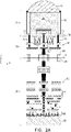
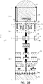
- Figs. 2A and 2B are schematic sectional views showing details of integrated optical transceivers, such as transceiver 20 ( Fig. 1 ), in accordance with embodiments of the invention. Both of these figures show a slice through dies 22, 24 and 26, including a single SPAD 28 and associated parts of Rx analog circuit 48 and Rx logic circuit 60. The two embodiments are very similar, and the description below applies to both embodiments unless noted otherwise.
- SPAD 28 comprises an anode contact 70 and cathode contacts 72, which are connected through metal vias 74 to Rx analog circuit 48.
- Each SPAD is isolated from its neighbors in the SPAD array by metal-filled backside deep trenches 76.
- Drive circuit 48 comprises high-voltage transistors 78, such as NMOS or PMOS thick-oxide transistors, with metal interconnects 80.
- a metal layer 82 for example a tungsten layer, extends across the back side of die 22. Metal layer 82 is useful in both enhancing the sensitivity of SPAD 28 and shielding Rx analog circuit 48 and other underlying circuits from incident photons, which could otherwise degrade the device performance.
- Hybrid bond 44 between dies 24 and 26 is formed by bonding together metal pads 84 and 86, for example copper pads, at the rear surface of die 24 and the front surface of die 26, respectively.
- Rx logic circuit 60 comprises CMOS logic 88, which is formed on a silicon substrate 90 of die 26. CMOS logic 88 is connected to Rx analog circuit 48 through metal layers 92 of die 26 and through pads 86 and 84.
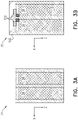
- Figs. 3A-3H are schematic sectional illustrations showing a sequence of manufacturing steps in fabrication of transceiver 20, in accordance with an example embodiment.
- the steps shown in these figures are typically carried out at the wafer level, and the resulting stack of three wafers is diced at the end of the process to create multiple transceiver chips.
- the figures show only a small part of the wafers, and the wafers are labeled in the figures as dies 22, 24 and 26, in correspondence with the description above.
- an array of SPADs 28 is fabricated in the upper silicon wafer (die 22) by appropriate doping of p and n regions, as is known in the art.
- Readout components 100 including gates and floating diffusion nodes, are deposited over SPADs 28, and are covered by an oxide layer 102, as shown in Fig. 3B .
- Die 22 is positioned upside-down in Figs. 3A through 3F , relative to its orientation in the preceding figures.
- an etch-stop layer 106 and a silicon layer 108 are deposited over a silicon substrate 104 of the middle wafer, as shown in Fig. 3C .
- Silicon layer 108 is covered by an oxide layer 110.
- the middle wafer is then flipped and oxide-bonded to oxide layer 102 at the top of the upper wafer, forming oxide bond 38, as shown in Fig. 3D .
- the back side of the middle wafer is thinned, for example by grinding and selective etching to remove silicon substrate 104 and etch-stop layer 106, as shown in Fig. 3E .
- the high-voltage circuits are then fabricated in the middle wafer, as shown in Fig. 3F .
- These circuits include transistors 78 (typically thick-oxide PMOS or NMOS) and other sensor driver components, as well as contacts and wiring, including vias 74 and interconnects 80. Copper pads 84 are deposited and etched at the upper side of the wafer (in this upside-down orientation) for purposes of hybrid bonding.
- transistors 78 typically thick-oxide PMOS or NMOS
- contacts and wiring including vias 74 and interconnects 80.
- Copper pads 84 are deposited and etched at the upper side of the wafer (in this upside-down orientation) for purposes of hybrid bonding.
- the circuits of logic 88 and metal layers 92 on substrate 90 of the bottom wafer (die 26) are fabricated separately, for example using a CMOS process. Copper pads 86 are similarly formed at the upper side of this wafer.
- the bonded upper and middle wafers (dies 22 and 24) are then flipped and overlaid on the bottom wafer (die 26), as shown in Fig. 3G .
- Pads 84 are aligned with pads 86, and the wafers are annealed to form hybrid bond 44 between the middle and bottom wafers.
- optical components such as wavelength filters 112 and microlenses 30, are fabricated over SPADs 28. The wafers are then diced to create multiple singulated transceivers 20.
- FIGs. 4A and 4B are schematic top and sectional views, respectively, of an optical transceiver device 120, in accordance with an embodiment of the invention.
- Device 120 comprises integrated optical transceiver 20, as described above, with VCSEL 52 on III-V semiconductor die 54 mounted on upper surface 32 of the transceiver chip.
- Transceiver 20 is mounted on a carrier substrate 122, such as a ceramic printed circuit board.
- transceiver 20 includes one or more reference SPADs 46, as noted above. These reference SPADs receive stray photons reflected from VCSEL 52 and thus provides a start signal for measurement of the time of flight of the photons received by SPADs 28 in array 33.
- a light block 128 within device 120 prevents optical crosstalk between VCSEL 52 and the SPADs in array 33.
- Figs. 5A and 5B are schematic top and sectional views, respectively, of an optical transceiver device 130, in accordance with another embodiment of the invention.
- III-V semiconductor die 54 with VCSEL 52 is mounted on carrier substrate 122 separately from a stacked SPAD chip 132.
- Chip 132 contains substantially the same components as transceiver 20, but Tx drive circuit 50 ( Fig. 1 ) outputs drive signals from SPAD chip 132 to III-V semiconductor die 54 via conductors 134 on carrier substrate 122, rather than via contacts on the SPAD chip itself.
- the operation of device 130 is similar to that of device 120 ( Figs. 4A/B ).
- the embodiments described above are directed specifically to dToF depth sensing, the principles of the present invention may similarly be applied, mutatis mutandis, in producing and operating other sorts of integrated optical transceivers, both for depth sensing and for other applications.
- the specific sorts of optical emitters and photodetectors that are used in the disclosed embodiments - i.e., a VCSEL emitter and an array of SPAD detectors - may be replaced, for example, by other types of avalanche diodes or single-photon detectors, as well as other types of pulsed optical emitters.
- the principles of the present invention may similarly be applied in producing stacked chips based on other sorts of semiconductors, such as III-V semiconductor dies.
- the present devices and methods may be adapted for use in the infrared, visible, or even ultraviolet range of optical radiation. All such alternative implementations and applications are considered to be within the scope of the present invention.
Landscapes
- Physics & Mathematics (AREA)
- Engineering & Computer Science (AREA)
- General Physics & Mathematics (AREA)
- Computer Networks & Wireless Communication (AREA)
- Remote Sensing (AREA)
- Radar, Positioning & Navigation (AREA)
- Electromagnetism (AREA)
- Optics & Photonics (AREA)
- Microelectronics & Electronic Packaging (AREA)
- Signal Processing (AREA)
- Condensed Matter Physics & Semiconductors (AREA)
- Solid State Image Pick-Up Elements (AREA)
- Light Receiving Elements (AREA)
Abstract
Description
- The present invention relates generally to optoelectronic devices and methods for their manufacture, and particularly to integrated optical transceivers.
- Sensors for direct time-of-flight (dToF) depth measurement typically include one or more laser emitters, such as vertical-cavity surface-emitting lasers (VCSELs), and an array of single-photon detectors, such as single-photon avalanche diodes (SPADs). The emitter or emitters direct light pulses toward a target scene, and the detectors output electrical pulses in response to incident photons that have been reflected from the scene. The timespans between an emitted light pulse and the resulting electrical pulses are indicative of the time of flight of the photons and thus of the distances to the points in the scene from which the photons were reflected.
- Embodiments of the present invention that are described hereinbelow provide integrated optical transceivers and methods for producing such transceivers.
- There is therefore provided, in accordance with an embodiment of the invention, an optoelectronic device, which includes a first semiconductor die, having first front and rear surfaces, and including at least one avalanche photodetector configured to output electrical pulses in response to photons incident on the first front surface. A second semiconductor die has a second front surface, which is bonded to the first rear surface, and a second rear surface, and includes a photodetector receiver analog circuit coupled to the at least one avalanche photodetector and an emitter driver circuit configured to drive a pulsed optical emitter. A third semiconductor die has a third front surface, which is bonded to the second rear surface, and a third rear surface, and includes logic circuits coupled to control the photodetector receiver analog circuit and the emitter driver circuit and to receive and process the electrical pulses output by the at least one avalanche photodetector.
- In some embodiments, the first, second, and third semiconductor dies include silicon dies. In some of these embodiments, the device includes a III-V semiconductor die, having fourth front and rear surfaces, and including the optical emitter, which is coupled to be driven by the emitter driver circuit and is configured to output optical pulses through the fourth front surface. In one embodiment, the optical emitter includes a vertical-cavity surface-emitting laser (VCSEL). Additionally or alternatively, the first semiconductor die includes first electrical contacts on the first front surface, and the III-V semiconductor die is mounted on the first front surface and includes second electrical contacts, which are connected to the first electrical contacts. In an alternative embodiment, the device includes a carrier substrate, wherein the III-V semiconductor die and the third semiconductor die are both mounted on the carrier substrate.
- In a disclosed embodiment, the at least one avalanche photodetector includes a single-photon avalanche detector (SPAD). Alternatively or additionally, the at least one avalanche photodetector includes an array of multiple photodetectors.
- In some embodiments, the first rear surface is bonded to the second front surface by an oxide bond. In a disclosed embodiment, the second rear surface and the third front surface include respective metal pads and are bonded together by hybrid bonding between the respective metal pads.
- Additionally or alternatively, the logic circuits in the third die include complementary metal-oxide-semiconductor (CMOS) logic, while the drive circuits in the second die include n-type metal-oxide-semiconductor (NMOS) transistors or p-type metal-oxide-semiconductor (PMOS) transistors.
- Further additionally or alternatively, the first semiconductor die includes a metal layer, which is disposed between the at least one avalanche photodetector and the first rear surface and shields the photodetector receiver analog circuit from the incident photons.
- There is also provided, in accordance with an embodiment of the invention, a method for fabricating an optoelectronic device. The method includes forming in a first semiconductor die at least one avalanche photodetector, which is configured to output electrical pulses in response to photons incident on a first front surface of the first semiconductor die. A second front surface of a second semiconductor die is bonded to a first rear surface of the first semiconductor die. A photodetector receiver analog circuit coupled to the at least one avalanche photodetector and an emitter driver circuit, which is configured to drive a pulsed optical emitter, are formed in the second semiconductor die. Logic circuits are formed in a third semiconductor die. A third front surface of the third semiconductor die is bonded to a second rear surface of the second semiconductor die so as to couple the logic circuits to control the photodetector receiver analog circuit and the emitter driver circuit and to receive and process the electrical pulses output by the at least one avalanche photodetector.
- The present invention will be more fully understood from the following detailed description of the embodiments thereof, taken together with the drawings in which:
-
-
Fig. 1 is a schematic sectional view of an integrated optical transceiver, in accordance with an embodiment of the invention; -
Figs. 2A and2B are schematic sectional views showing details of integrated optical transceivers, in accordance with embodiments of the invention; -
Figs. 3A, 3B ,3C, 3D ,3E ,3F, 3G and 3H are schematic sectional views showing a sequence of manufacturing steps in fabrication of a stacked optical transceiver chip, in accordance with an embodiment of the invention; and -
Figs. 4A and 4B are schematic top and sectional views, respectively, of an optical transceiver device, in accordance with an embodiment of the invention; and -
Figs. 5A and 5B are schematic top and sectional views, respectively, of an optical transceiver device, in accordance with another embodiment of the invention. - For mass-market applications of dToF depth sensing, it is desirable that the sensor be made as small and inexpensive as possible. For this purpose, for example, all driving and control functions should be integrated on a single silicon chip together with an array of single-photon detectors, such as SPADs. The emitters, such as VCSELs, are typically fabricated on a separate III-V semiconductor substrate, such as GaAs, but can be mounted either on top of the silicon chip, for example using VCSEL-on-silicon technologies, or alongside the silicon chip in close proximity. The emitter (Tx) and detector (Rx) circuits can then share circuit elements such as a phase-locked loop (PLL), temperature sensor, high-voltage bias circuitry, control and interface logic, and memory, thus reducing the overall chip area. Creating this sort of integrated chip is difficult, however, because of the need to integrate and accommodate the diverse requirements of optoelectronics, high-voltage drive components, and high-speed logic.
- Embodiments of the present invention that are described herein address this problem using three silicon wafers that are stacked and bonded together. After fabricating the device components and bonding the wafers together, the bonded wafers are diced to produce multiple integrated transceiver chips. Each such chip thus comprises three semiconductor dies:
- The first semiconductor die comprises at least one avalanche photodetector, which outputs electrical pulses in response to photons incident on the front surface of the die. In the embodiments described below, the first die comprises an array of photodetectors, such as SPADs, which enables the devices to sense incoming photons with finer spatial resolution and/or wider dynamic range.
- The front surface of the second semiconductor die is bonded to the rear surface of the first semiconductor die, for example by oxide bonding (also referred to as sequential bonding). This second die comprises high-voltage circuits, including a photodetector receiver analog circuit coupled to the photodetectors in the first die and an emitter driver circuit, for driving a pulsed optical emitter, such as a VCSEL.
- The front surface of the third semiconductor die is bonded to the rear surface of the second semiconductor die, for example by hybrid bonding between metal pads at the two surfaces. The third die comprises low-voltage logic circuits, which control the photodetector receiver analog circuit and the emitter driver circuit, and which receive and process the electrical pulses output by the photodetectors.
- The terms "high-voltage" and "low-voltage" are used in a relative sense, as the ranges of "high" and "low" voltages depend on the technologies that are used. For example, considering technologies that are currently available, the logic circuits in the third die may comprise complementary metal-oxide-semiconductor (CMOS) logic, which operates at voltages in the range of 0.7-3 volts; while the drive circuits in the second die comprise n-type metal-oxide-semiconductor (NMOS) transistors or p-type metal-oxide-semiconductor (PMOS) transistors with thick oxide layers, operating in the range of 3-10 volts. Alternatively, higher or lower voltage ranges may be used. In any case, the application of different circuit technologies in the second and third dies enables the stacked chip to carry out both the high-voltage driving functions and the high-speed logic functions that are involved in operation of the optical transceiver.
- In some embodiments, the optical emitter is formed on a III-V semiconductor die, such as a GaAs die, which may be mounted either on a part of the front surface of the first (silicon) die or alongside the stacked chip on a carrier substrate. In either case, combining the detector (Rx) and emitter driving (Tx) functions in a single stacked chip of this sort reduces the net die area in several ways:
- It eliminates the inter-die interface circuits that are needed when the Rx and Tx driving functions are implemented in separate chips, and it reduces the complexity of the logic.
- It reduces the total pad count of the device, since many pads (such as clock, power supply, and control lines) can be shared by the Rx and Tx circuits.
- It enables the Rx and Tx drivers to share high-speed analog and digital circuits, such as oscillators, phase-locked loops (PLLs), and/or delay-locked loops (DLLs).
-
Fig. 1 is a schematic sectional view of an integratedoptical transceiver 20, in accordance with an embodiment of the invention.Transceiver 20 comprises an integrated circuit (IC) chip made up of three semiconductor dies 22, 24 and 26, for example silicon dies, which are stacked and bonded together. The components oftransceiver 20 are shown conceptually inFig. 1 and are not drawn to scale. -
SPADs 28 indie 22 receive photons throughrespective microlenses 30 on afront surface 32 ofdie 22 and output electrical pulses in response to the incident photons. (The term "front" is used in the context of the present description and in the claims, for the sake of convenience and clarity, to refer to the side oftransceiver 20 through which photons are received, while "rear" refers to the opposite side.) Although a single row ofSPADs 28 is shown in this figure, die 22 may comprise a smaller or larger number of SPADs, from a single SPAD up to a two-dimensional array 33 including tens, hundreds, or even thousands of SPADs. Arear surface 34 ofdie 22 is bonded to afront surface 36 ofdie 24, for example by an oxide (sequential)bond 38. Arear surface 40 ofdie 24 is bonded to afront surface 42 ofdie 26, for example by ahybrid bond 44. For the sake of convenience and clarity in the description that follows, the surfaces of the dies (such assurfaces -
Die 24 comprises a photodetector receiver (Rx)analog circuit 48, which is coupled toSPADs 28, and an emitter (Tx) drivecircuit 50, which drives a pulsed optical emitter, such as aVCSEL 52. In the pictured embodiment, die 22 also contains areference SPAD 46, or an array of reference SPADs, which are also driven byRx analog circuit 48. The purpose ofreference SPAD 46 is explained further hereinbelow.Rx analog circuit 48 performs functions that include biasing, quenching, and rechargingSPADs VCSEL 52 is fabricated on a III-V semiconductor die 54, such as a GaAs die, which is then mounted onfront surface 32 ofdie 22 and is attached byelectrical contacts 56 to Tx drivecircuit 50.Contacts 56 comprise, for example, suitable metal bumps, which are connected by vias 58 to Tx drivecircuit 50. The Tx drive circuit outputs short high-voltage electrical pulses, which causeVCSEL 52 to emit short, high-intensity optical pulses. -
Die 26 comprisesRx logic circuits 60, which control and receive signals fromRx analog circuit 48, andTx logic circuits 62, which controlTx drive circuit 50. The locations and relative areas ofRx logic circuits 60 andTx logic circuits 62 need not match those of the drive circuits indie 24.Tx logic circuits 62 control the timing of the sequence of optical pulses emitted byVCSEL 52.Rx logic circuits 60 receive and process the electrical pulses output bySPADs 28 in order to count the incident photons and measure their timing relative to the outgoing optical pulses. Sharedcircuits 64 indie 26 perform high-speed timing and digital logic functions that are shared by and coordinate betweenRx logic circuits 60 andTx logic circuits 62. Sharedcircuits 64 may include, for example, one or more oscillators, PLLs, and/or DLLs, as well as memory and input/output circuits. -
Figs. 2A and2B are schematic sectional views showing details of integrated optical transceivers, such as transceiver 20 (Fig. 1 ), in accordance with embodiments of the invention. Both of these figures show a slice through dies 22, 24 and 26, including asingle SPAD 28 and associated parts ofRx analog circuit 48 andRx logic circuit 60. The two embodiments are very similar, and the description below applies to both embodiments unless noted otherwise. -
SPAD 28 comprises ananode contact 70 andcathode contacts 72, which are connected throughmetal vias 74 toRx analog circuit 48. Each SPAD is isolated from its neighbors in the SPAD array by metal-filled backsidedeep trenches 76. Drivecircuit 48 comprises high-voltage transistors 78, such as NMOS or PMOS thick-oxide transistors, with metal interconnects 80. In the embodiment ofFig. 2B , ametal layer 82, for example a tungsten layer, extends across the back side ofdie 22.Metal layer 82 is useful in both enhancing the sensitivity ofSPAD 28 and shieldingRx analog circuit 48 and other underlying circuits from incident photons, which could otherwise degrade the device performance. -
Hybrid bond 44 between dies 24 and 26 is formed by bonding togethermetal pads die 24 and the front surface ofdie 26, respectively.Rx logic circuit 60 comprisesCMOS logic 88, which is formed on asilicon substrate 90 ofdie 26.CMOS logic 88 is connected toRx analog circuit 48 throughmetal layers 92 ofdie 26 and throughpads -
Figs. 3A-3H are schematic sectional illustrations showing a sequence of manufacturing steps in fabrication oftransceiver 20, in accordance with an example embodiment. The steps shown in these figures are typically carried out at the wafer level, and the resulting stack of three wafers is diced at the end of the process to create multiple transceiver chips. For the sake of simplicity, however, the figures show only a small part of the wafers, and the wafers are labeled in the figures as dies 22, 24 and 26, in correspondence with the description above. - Beginning with
Fig. 3A , an array ofSPADs 28 is fabricated in the upper silicon wafer (die 22) by appropriate doping of p and n regions, as is known in the art.Readout components 100, including gates and floating diffusion nodes, are deposited overSPADs 28, and are covered by anoxide layer 102, as shown inFig. 3B . (Die 22 is positioned upside-down inFigs. 3A through 3F , relative to its orientation in the preceding figures.) - In preparation for processing of
die 24, an etch-stop layer 106 and asilicon layer 108 are deposited over asilicon substrate 104 of the middle wafer, as shown inFig. 3C .Silicon layer 108 is covered by anoxide layer 110. The middle wafer is then flipped and oxide-bonded tooxide layer 102 at the top of the upper wafer, formingoxide bond 38, as shown inFig. 3D . After bonding, the back side of the middle wafer is thinned, for example by grinding and selective etching to removesilicon substrate 104 and etch-stop layer 106, as shown inFig. 3E . The high-voltage circuits are then fabricated in the middle wafer, as shown inFig. 3F . These circuits include transistors 78 (typically thick-oxide PMOS or NMOS) and other sensor driver components, as well as contacts and wiring, includingvias 74 and interconnects 80.Copper pads 84 are deposited and etched at the upper side of the wafer (in this upside-down orientation) for purposes of hybrid bonding. - The circuits of
logic 88 andmetal layers 92 onsubstrate 90 of the bottom wafer (die 26) are fabricated separately, for example using a CMOS process.Copper pads 86 are similarly formed at the upper side of this wafer. The bonded upper and middle wafers (dies 22 and 24) are then flipped and overlaid on the bottom wafer (die 26), as shown inFig. 3G .Pads 84 are aligned withpads 86, and the wafers are annealed to formhybrid bond 44 between the middle and bottom wafers. Finally, optical components, such as wavelength filters 112 andmicrolenses 30, are fabricated overSPADs 28. The wafers are then diced to create multiplesingulated transceivers 20. -
Figs. 4A and 4B are schematic top and sectional views, respectively, of anoptical transceiver device 120, in accordance with an embodiment of the invention.Device 120 comprises integratedoptical transceiver 20, as described above, withVCSEL 52 on III-V semiconductor die 54 mounted onupper surface 32 of the transceiver chip.Transceiver 20 is mounted on acarrier substrate 122, such as a ceramic printed circuit board. -
VCSEL 52 emits photons through anexit window 124 toward a target scene. Photons reflected from the target scene are incident onarray 33 ofSPADs 28 via anentrance window 126. In addition toarray 33,transceiver 20 includes one ormore reference SPADs 46, as noted above. These reference SPADs receive stray photons reflected fromVCSEL 52 and thus provides a start signal for measurement of the time of flight of the photons received bySPADs 28 inarray 33. Alight block 128 withindevice 120 prevents optical crosstalk betweenVCSEL 52 and the SPADs inarray 33. -
Figs. 5A and 5B are schematic top and sectional views, respectively, of anoptical transceiver device 130, in accordance with another embodiment of the invention. In this embodiment, III-V semiconductor die 54 withVCSEL 52 is mounted oncarrier substrate 122 separately from astacked SPAD chip 132.Chip 132 contains substantially the same components astransceiver 20, but Tx drive circuit 50 (Fig. 1 ) outputs drive signals fromSPAD chip 132 to III-V semiconductor die 54 viaconductors 134 oncarrier substrate 122, rather than via contacts on the SPAD chip itself. In other respects, the operation ofdevice 130 is similar to that of device 120 (Figs. 4A/B ). - Although the embodiments described above are directed specifically to dToF depth sensing, the principles of the present invention may similarly be applied, mutatis mutandis, in producing and operating other sorts of integrated optical transceivers, both for depth sensing and for other applications. Thus, the specific sorts of optical emitters and photodetectors that are used in the disclosed embodiments - i.e., a VCSEL emitter and an array of SPAD detectors - may be replaced, for example, by other types of avalanche diodes or single-photon detectors, as well as other types of pulsed optical emitters. Furthermore, although silicon technologies are currently best suited for producing the stacked chips described above, the principles of the present invention may similarly be applied in producing stacked chips based on other sorts of semiconductors, such as III-V semiconductor dies. By appropriate choices of materials and technologies, the present devices and methods may be adapted for use in the infrared, visible, or even ultraviolet range of optical radiation. All such alternative implementations and applications are considered to be within the scope of the present invention.
- It will thus be appreciated that the embodiments described above are cited by way of example, and that the present invention is not limited to what has been particularly shown and described hereinabove. Rather, the scope of the present invention includes both combinations and subcombinations of the various features described hereinabove, as well as variations and modifications thereof which would occur to persons skilled in the art upon reading the foregoing description and which are not disclosed in the prior art.
Claims (15)
- An optoelectronic device (20), comprising:a first semiconductor die (22), having first front and rear surfaces (32, 34), and comprising at least one avalanche photodetector (28) configured to output electrical pulses in response to photons incident on the first front surface;a second semiconductor die (24), having a second front surface (36), which is bonded to the first rear surface, and a second rear surface (40) and comprising a photodetector receiver analog circuit (48) coupled to the at least one avalanche photodetector and an emitter driver circuit (50) configured to drive a pulsed optical emitter (52); anda third semiconductor die (26), having a third front surface (42), which is bonded to the second rear surface, and a third rear surface, and comprising logic circuits (60, 62, 64) coupled to control the photodetector receiver analog circuit and the emitter driver circuit and to receive and process the electrical pulses output by the at least one avalanche photodetector.
- The device according to claim 1, wherein the first, second, and third semiconductor dies comprise silicon dies.
- The device according to claim 2, and comprising a III-V semiconductor die, having fourth front and rear surfaces, and comprising the optical emitter, which is coupled to be driven by the emitter driver circuit and is configured to output optical pulses through the fourth front surface.
- The device according to claim 3, wherein the optical emitter comprises a vertical-cavity surface-emitting laser (VCSEL) .
- The device according to claim 3, wherein the first semiconductor die comprises first electrical contacts on the first front surface, and wherein the III-V semiconductor die is mounted on the first front surface and comprises second electrical contacts, which are connected to the first electrical contacts.
- The device according to claim 3, and comprising a carrier substrate, wherein the III-V semiconductor die and the third semiconductor die are both mounted on the carrier substrate.
- The device according to any of claims 1-6, wherein the at least one avalanche photodetector comprises a single-photon avalanche detector (SPAD).
- The device according to any of claims 1-6, wherein the at least one avalanche photodetector comprises an array of multiple photodetectors.
- The device according to any of claims 1-6, wherein the first rear surface is bonded to the second front surface by an oxide bond.
- The device according to claim 9, wherein the second rear surface and the third front surface comprise respective metal pads and are bonded together by hybrid bonding between the respective metal pads.
- The device according to any of claims 1-6, wherein the logic circuits in the third die comprise complementary metal-oxide-semiconductor (CMOS) logic, while the drive circuits in the second die comprise n-type metal-oxide-semiconductor (NMOS) transistors or p-type metal-oxide-semiconductor (PMOS) transistors.
- The device according to any of claims 1-6, wherein the first semiconductor die comprises a metal layer, which is disposed between the at least one avalanche photodetector and the first rear surface and shields the photodetector receiver analog circuit from the incident photons.
- A method for fabricating an optoelectronic device (20), the method comprising:forming in a first semiconductor die (22) at least one avalanche photodetector (28), which is configured to output electrical pulses in response to photons incident on a first front surface (32) of the first semiconductor die;bonding a second front surface (36) of a second semiconductor die (24) to a first rear surface (34) of the first semiconductor die;forming in the second semiconductor die a photodetector receiver analog circuit (48) coupled to the at least one avalanche photodetector and an emitter driver circuit (50), which is configured to drive a pulsed optical emitter (52);forming logic circuits (60, 62, 64) in a third semiconductor die (26); andbonding a third front surface (42) of the third semiconductor die to a second rear surface (40) of the second semiconductor die so as to couple the logic circuits to control the photodetector receiver analog circuit and the emitter driver circuit and to receive and process the electrical pulses output by the at least one avalanche photodetector.
- The method according to claim 13, wherein the first, second, and third semiconductor dies comprise silicon dies.
- The method according to claim 14, and comprising coupling a III-V semiconductor die, having fourth front and rear surfaces and comprising the optical emitter, to be driven by the emitter driver circuit so as to output optical pulses through the fourth front surface.
Applications Claiming Priority (2)
| Application Number | Priority Date | Filing Date | Title |
|---|---|---|---|
| US202163211020P | 2021-06-16 | 2021-06-16 | |
| US202163245878P | 2021-09-19 | 2021-09-19 |
Publications (2)
| Publication Number | Publication Date |
|---|---|
| EP4105684A1 true EP4105684A1 (en) | 2022-12-21 |
| EP4105684B1 EP4105684B1 (en) | 2025-12-10 |
Family
ID=81387281
Family Applications (1)
| Application Number | Title | Priority Date | Filing Date |
|---|---|---|---|
| EP22169910.1A Active EP4105684B1 (en) | 2021-06-16 | 2022-04-26 | Single-chip optical transceiver |
Country Status (4)
| Country | Link |
|---|---|
| US (1) | US12429565B2 (en) |
| EP (1) | EP4105684B1 (en) |
| KR (1) | KR102916906B1 (en) |
| CN (1) | CN115480231B (en) |
Cited By (1)
| Publication number | Priority date | Publication date | Assignee | Title |
|---|---|---|---|---|
| DE102025101795A1 (en) * | 2024-12-06 | 2026-06-11 | GM Global Technology Operations LLC | Sensor with high-resolution SPAD array for lidar using a micro-assembly process |
Families Citing this family (6)
| Publication number | Priority date | Publication date | Assignee | Title |
|---|---|---|---|---|
| US12386045B1 (en) | 2021-02-16 | 2025-08-12 | Apple Inc. | Enhanced LiDAR measurements using chirp nonlinearities |
| US11927814B2 (en) * | 2022-01-05 | 2024-03-12 | Scidatek Inc. | Semiconductor photodetector array sensor integrated with optical-waveguide-based devices |
| US12498462B2 (en) | 2022-05-12 | 2025-12-16 | Apple Inc. | LiDAR array with vertically-coupled transceivers |
| US12656496B2 (en) | 2022-06-12 | 2026-06-16 | Apple Inc. | Coherent sensing system using a DOE |
| US12699228B2 (en) | 2022-08-07 | 2026-08-04 | Apple Inc. | Grating coupler with high efficiency |
| US12653423B1 (en) | 2023-08-27 | 2026-06-16 | Apple Inc. | Multi-mode sensor for object identification |
Citations (3)
| Publication number | Priority date | Publication date | Assignee | Title |
|---|---|---|---|---|
| US20200309955A1 (en) * | 2017-12-18 | 2020-10-01 | Apple Inc. | Time-of-flight sensing using an addressable array of emitters |
| US20210159108A1 (en) * | 2010-11-18 | 2021-05-27 | Monolithic 3D Inc. | Method for processing a 3d integrated circuit and structure |
| US20210167572A1 (en) * | 2018-08-22 | 2021-06-03 | Sony Semiconductor Solutions Corporation | Light source apparatus, temperature detection method, and sensing module |
Family Cites Families (31)
| Publication number | Priority date | Publication date | Assignee | Title |
|---|---|---|---|---|
| US5753928A (en) | 1993-09-30 | 1998-05-19 | Siemens Components, Inc. | Monolithic optical emitter-detector |
| US5567955A (en) | 1995-05-04 | 1996-10-22 | National Research Council Of Canada | Method for infrared thermal imaging using integrated gasa quantum well mid-infrared detector and near-infrared light emitter and SI charge coupled device |
| US5780867A (en) | 1996-03-07 | 1998-07-14 | Sandia Corporation | Broadband light-emitting diode |
| US6028323A (en) | 1996-07-19 | 2000-02-22 | National Research Council Of Canada | Quantum well infared image conversion panel and associated methods |
| KR20050019484A (en) | 2003-08-19 | 2005-03-03 | 삼성전자주식회사 | Long wavelength Vertical Cavity Surface Emitting Laser with monolithically-growth photodetector |
| KR20050019485A (en) | 2003-08-19 | 2005-03-03 | 삼성전자주식회사 | Vertical cavity Surface Emitting Laser with integrated photodetector |
| CA2447828C (en) | 2003-10-15 | 2012-07-03 | National Research Council Of Canada | Wavelength conversion device with avalanche multiplier |
| WO2009138912A2 (en) | 2008-05-16 | 2009-11-19 | Philips Intellectual Property & Standards Gmbh | Security system comprising a self-mixing laser sensor and method of driving such a security system |
| US9331096B2 (en) | 2009-09-04 | 2016-05-03 | Luxtera, Inc. | Method and system for hybrid integration of optical communication systems |
| US10090349B2 (en) | 2012-08-09 | 2018-10-02 | Taiwan Semiconductor Manufacturing Company, Ltd. | CMOS image sensor chips with stacked scheme and methods for forming the same |
| US8629524B2 (en) | 2012-04-27 | 2014-01-14 | Taiwan Semiconductor Manufacturing Company, Ltd. | Apparatus for vertically integrated backside illuminated image sensors |
| JP2014035546A (en) | 2012-08-07 | 2014-02-24 | Luxtera Inc | Method and system for hybrid integration of optical communication system |
| CN104123179A (en) | 2013-04-29 | 2014-10-29 | 敦南科技股份有限公司 | Interrupt control method and electronic system thereof |
| US9331116B2 (en) | 2014-01-15 | 2016-05-03 | Omnivision Technologies, Inc. | Back side illuminated single photon avalanche diode imaging sensor with high short wavelength detection efficiency |
| EP3128743B1 (en) | 2014-03-31 | 2025-05-21 | Nikon Corporation | Detection element, lock-in detection device, substrate, and manufacturing method for detection element |
| KR20160058591A (en) * | 2014-11-17 | 2016-05-25 | 에스케이하이닉스 주식회사 | Semiconductor package having optical interconnect |
| EP3091271B1 (en) | 2015-05-05 | 2018-07-11 | Sick Ag | Light sensor |
| US9806067B2 (en) * | 2015-07-20 | 2017-10-31 | Globalfoundries Inc. | Die-die stacking |
| EP3497757A1 (en) | 2016-09-19 | 2019-06-19 | Apple Inc. | Vertical emitters integrated on silicon control backplane |
| EP3316497B1 (en) * | 2016-10-26 | 2019-10-16 | STMicroelectronics (Research & Development) Limited | A single photon avalanche diode module for communications |
| CN106531822B (en) | 2016-11-29 | 2017-12-19 | 电子科技大学 | A kind of photodetector |
| US10411146B1 (en) | 2017-01-06 | 2019-09-10 | United States Of America As Represented By The Secretary Of The Air Force | High absorption infrared superlattices |
| WO2018191495A1 (en) * | 2017-04-12 | 2018-10-18 | Sense Photonics, Inc. | Beam shaping for ultra-small vertical cavity surface emitting laser (vcsel) arrays |
| EP3622314A4 (en) | 2017-08-31 | 2021-04-14 | SZ DJI Technology Co., Ltd. | Systems and methods for an apd array solid-state laser radar |
| US10636930B2 (en) | 2017-09-29 | 2020-04-28 | Taiwan Semiconductor Manufacturing Company Ltd. | SPAD image sensor and associated fabricating method |
| EP3588700A1 (en) | 2018-06-26 | 2020-01-01 | Koninklijke Philips N.V. | Vcsel device for an smi sensor for recording three-dimensional pictures |
| CN109786413B (en) | 2019-02-14 | 2021-03-02 | 豪威半导体(上海)有限责任公司 | Image sensor with a plurality of pixels |
| US12007504B2 (en) | 2019-03-01 | 2024-06-11 | Vixar, Inc. | 3D and LiDAR sensing modules |
| CN110196106B (en) | 2019-05-20 | 2021-06-15 | 北京师范大学 | Single Photon Avalanche Photodiode Array Detectors |
| US11549799B2 (en) | 2019-07-01 | 2023-01-10 | Apple Inc. | Self-mixing interference device for sensing applications |
| US11322630B2 (en) | 2019-09-23 | 2022-05-03 | Apple Inc. | Monolithic infrared transceiver |
-
2022
- 2022-04-06 US US17/714,161 patent/US12429565B2/en active Active
- 2022-04-26 EP EP22169910.1A patent/EP4105684B1/en active Active
- 2022-05-25 KR KR1020220064043A patent/KR102916906B1/en active Active
- 2022-05-30 CN CN202210595722.0A patent/CN115480231B/en active Active
Patent Citations (3)
| Publication number | Priority date | Publication date | Assignee | Title |
|---|---|---|---|---|
| US20210159108A1 (en) * | 2010-11-18 | 2021-05-27 | Monolithic 3D Inc. | Method for processing a 3d integrated circuit and structure |
| US20200309955A1 (en) * | 2017-12-18 | 2020-10-01 | Apple Inc. | Time-of-flight sensing using an addressable array of emitters |
| US20210167572A1 (en) * | 2018-08-22 | 2021-06-03 | Sony Semiconductor Solutions Corporation | Light source apparatus, temperature detection method, and sensing module |
Cited By (1)
| Publication number | Priority date | Publication date | Assignee | Title |
|---|---|---|---|---|
| DE102025101795A1 (en) * | 2024-12-06 | 2026-06-11 | GM Global Technology Operations LLC | Sensor with high-resolution SPAD array for lidar using a micro-assembly process |
Also Published As
| Publication number | Publication date |
|---|---|
| KR102916906B1 (en) | 2026-01-26 |
| US20220404475A1 (en) | 2022-12-22 |
| EP4105684B1 (en) | 2025-12-10 |
| CN115480231A (en) | 2022-12-16 |
| US12429565B2 (en) | 2025-09-30 |
| CN115480231B (en) | 2026-06-19 |
| KR20220168553A (en) | 2022-12-23 |
Similar Documents
| Publication | Publication Date | Title |
|---|---|---|
| US12429565B2 (en) | Single-chip optical transceiver | |
| EP4111559B1 (en) | 3d and lidar sensing modules | |
| US8320423B2 (en) | Compact, all solid-state, avalanche photodiode emitter-detector pixel with electronically selectable, passive or active detection mode, for large-scale, high resolution, imaging focal plane arrays | |
| CN104779259B (en) | The single-photon avalanche diode imaging sensor applied for complementary metal oxide semiconductor stacked chips | |
| US12360219B2 (en) | MicroLED based time of flight system | |
| WO2001097294A2 (en) | Integrated electronic-optoelectronic devices and method of making the same | |
| CN109786413B (en) | Image sensor with a plurality of pixels | |
| CN110178044A (en) | Lidar | |
| US20230411926A1 (en) | Multi-wafer integrated vcsel-electronics module | |
| WO2019246134A2 (en) | Apparatus and method for optical sensing using an optoelectronic device and optoelectronic device arrays | |
| US20250359365A1 (en) | Method of manufacturing photodetector module comprising emitter and receiver | |
| US20250355091A1 (en) | Method of manufacturing lidar sensor for mobile device | |
| US6872983B2 (en) | High speed optical transceiver package using heterogeneous integration | |
| US8785897B2 (en) | Monolithic opto-isolators | |
| CN114551412A (en) | Crosstalk-free indium gallium arsenic Geiger mode focal plane detection chip structure and manufacturing method thereof | |
| US20250228017A1 (en) | High-sensitivity avalanche photodetectors with feedback structures | |
| EP3435428B1 (en) | Light emitting semiconductor device for generation of short light pulses | |
| CN113437173A (en) | Photodetector, photodetection system, laser radar device, and vehicle | |
| Carson et al. | Low-power modular parallel photonic data links | |
| US20250354863A1 (en) | Avalanche diode arrangement, electronic device and method for controlling an avalanche diode arrangement | |
| US20250112189A1 (en) | Die and Wafer Level Processing of Laser Diodes and Other Semiconductor Devices on Non-Native Semiconductor Wafers | |
| US11978814B2 (en) | Superlattice photo detector | |
| US20240094349A1 (en) | Light detector, light detection system, and lidar device | |
| Zuo et al. | Design and process optimization of a FSI SPAD for LiDAR applications in 55nm BCD technology | |
| JP2024041597A (en) | Optical detector, optical detection system, lidar device, and moving object |
Legal Events
| Date | Code | Title | Description |
|---|---|---|---|
| PUAI | Public reference made under article 153(3) epc to a published international application that has entered the european phase |
Free format text: ORIGINAL CODE: 0009012 |
|
| STAA | Information on the status of an ep patent application or granted ep patent |
Free format text: STATUS: REQUEST FOR EXAMINATION WAS MADE |
|
| 17P | Request for examination filed |
Effective date: 20220426 |
|
| AK | Designated contracting states |
Kind code of ref document: A1 Designated state(s): AL AT BE BG CH CY CZ DE DK EE ES FI FR GB GR HR HU IE IS IT LI LT LU LV MC MK MT NL NO PL PT RO RS SE SI SK SM TR |
|
| REG | Reference to a national code |
Ref country code: DE Ref legal event code: R079 Free format text: PREVIOUS MAIN CLASS: G01S0007483000 Ipc: G01S0017890000 Ref document number: 602022026423 Country of ref document: DE |
|
| GRAP | Despatch of communication of intention to grant a patent |
Free format text: ORIGINAL CODE: EPIDOSNIGR1 |
|
| STAA | Information on the status of an ep patent application or granted ep patent |
Free format text: STATUS: GRANT OF PATENT IS INTENDED |
|
| RIC1 | Information provided on ipc code assigned before grant |
Ipc: G01S 17/89 20200101AFI20250710BHEP Ipc: G01S 17/10 20200101ALI20250710BHEP Ipc: G01S 17/894 20200101ALI20250710BHEP Ipc: G01S 7/483 20060101ALI20250710BHEP Ipc: G01S 7/484 20060101ALI20250710BHEP Ipc: G01S 7/486 20200101ALI20250710BHEP |
|
| INTG | Intention to grant announced |
Effective date: 20250721 |
|
| RIN1 | Information on inventor provided before grant (corrected) |
Inventor name: LAFLAQUIERE, ARNAUD Inventor name: NICLASS, CRISTIANO L. Inventor name: DRADER, MARC |
|
| GRAS | Grant fee paid |
Free format text: ORIGINAL CODE: EPIDOSNIGR3 |
|
| GRAA | (expected) grant |
Free format text: ORIGINAL CODE: 0009210 |
|
| STAA | Information on the status of an ep patent application or granted ep patent |
Free format text: STATUS: THE PATENT HAS BEEN GRANTED |
|
| AK | Designated contracting states |
Kind code of ref document: B1 Designated state(s): AL AT BE BG CH CY CZ DE DK EE ES FI FR GB GR HR HU IE IS IT LI LT LU LV MC MK MT NL NO PL PT RO RS SE SI SK SM TR |
|
| REG | Reference to a national code |
Ref country code: CH Ref legal event code: F10 Free format text: ST27 STATUS EVENT CODE: U-0-0-F10-F00 (AS PROVIDED BY THE NATIONAL OFFICE) Effective date: 20251210 Ref country code: GB Ref legal event code: FG4D |
|
| REG | Reference to a national code |
Ref country code: DE Ref legal event code: R096 Ref document number: 602022026423 Country of ref document: DE |
|
| REG | Reference to a national code |
Ref country code: IE Ref legal event code: FG4D |
|
| P01 | Opt-out of the competence of the unified patent court (upc) registered |
Free format text: CASE NUMBER: UPC_APP_0017458_4105684/2025 Effective date: 20251212 |
|
| PG25 | Lapsed in a contracting state [announced via postgrant information from national office to epo] |
Ref country code: ES Free format text: LAPSE BECAUSE OF FAILURE TO SUBMIT A TRANSLATION OF THE DESCRIPTION OR TO PAY THE FEE WITHIN THE PRESCRIBED TIME-LIMIT Effective date: 20251210 |
|
| REG | Reference to a national code |
Ref country code: LT Ref legal event code: MG9D |
|
| PG25 | Lapsed in a contracting state [announced via postgrant information from national office to epo] |
Ref country code: NO Free format text: LAPSE BECAUSE OF FAILURE TO SUBMIT A TRANSLATION OF THE DESCRIPTION OR TO PAY THE FEE WITHIN THE PRESCRIBED TIME-LIMIT Effective date: 20260310 |
|
| PG25 | Lapsed in a contracting state [announced via postgrant information from national office to epo] |
Ref country code: HR Free format text: LAPSE BECAUSE OF FAILURE TO SUBMIT A TRANSLATION OF THE DESCRIPTION OR TO PAY THE FEE WITHIN THE PRESCRIBED TIME-LIMIT Effective date: 20251210 Ref country code: FI Free format text: LAPSE BECAUSE OF FAILURE TO SUBMIT A TRANSLATION OF THE DESCRIPTION OR TO PAY THE FEE WITHIN THE PRESCRIBED TIME-LIMIT Effective date: 20251210 |
|
| REG | Reference to a national code |
Ref country code: NL Ref legal event code: MP Effective date: 20251210 |
|
| PG25 | Lapsed in a contracting state [announced via postgrant information from national office to epo] |
Ref country code: RS Free format text: LAPSE BECAUSE OF FAILURE TO SUBMIT A TRANSLATION OF THE DESCRIPTION OR TO PAY THE FEE WITHIN THE PRESCRIBED TIME-LIMIT Effective date: 20260310 |
|
| PG25 | Lapsed in a contracting state [announced via postgrant information from national office to epo] |
Ref country code: LV Free format text: LAPSE BECAUSE OF FAILURE TO SUBMIT A TRANSLATION OF THE DESCRIPTION OR TO PAY THE FEE WITHIN THE PRESCRIBED TIME-LIMIT Effective date: 20251210 |
|
| PG25 | Lapsed in a contracting state [announced via postgrant information from national office to epo] |
Ref country code: BG Free format text: LAPSE BECAUSE OF FAILURE TO SUBMIT A TRANSLATION OF THE DESCRIPTION OR TO PAY THE FEE WITHIN THE PRESCRIBED TIME-LIMIT Effective date: 20251210 |
|
| REG | Reference to a national code |
Ref country code: AT Ref legal event code: MK05 Ref document number: 1866697 Country of ref document: AT Kind code of ref document: T Effective date: 20251210 |
|
| PG25 | Lapsed in a contracting state [announced via postgrant information from national office to epo] |
Ref country code: NL Free format text: LAPSE BECAUSE OF FAILURE TO SUBMIT A TRANSLATION OF THE DESCRIPTION OR TO PAY THE FEE WITHIN THE PRESCRIBED TIME-LIMIT Effective date: 20251210 |
|
| PG25 | Lapsed in a contracting state [announced via postgrant information from national office to epo] |
Ref country code: LT Free format text: LAPSE BECAUSE OF FAILURE TO SUBMIT A TRANSLATION OF THE DESCRIPTION OR TO PAY THE FEE WITHIN THE PRESCRIBED TIME-LIMIT Effective date: 20251210 |
|
| PG25 | Lapsed in a contracting state [announced via postgrant information from national office to epo] |
Ref country code: SM Free format text: LAPSE BECAUSE OF FAILURE TO SUBMIT A TRANSLATION OF THE DESCRIPTION OR TO PAY THE FEE WITHIN THE PRESCRIBED TIME-LIMIT Effective date: 20251210 |
|
| PG25 | Lapsed in a contracting state [announced via postgrant information from national office to epo] |
Ref country code: PL Free format text: LAPSE BECAUSE OF FAILURE TO SUBMIT A TRANSLATION OF THE DESCRIPTION OR TO PAY THE FEE WITHIN THE PRESCRIBED TIME-LIMIT Effective date: 20251210 |
|
| PG25 | Lapsed in a contracting state [announced via postgrant information from national office to epo] |
Ref country code: IT Free format text: LAPSE BECAUSE OF FAILURE TO SUBMIT A TRANSLATION OF THE DESCRIPTION OR TO PAY THE FEE WITHIN THE PRESCRIBED TIME-LIMIT Effective date: 20251210 |
|
| PGFP | Annual fee paid to national office [announced via postgrant information from national office to epo] |
Ref country code: DE Payment date: 20260226 Year of fee payment: 5 |
|
| PG25 | Lapsed in a contracting state [announced via postgrant information from national office to epo] |
Ref country code: AT Free format text: LAPSE BECAUSE OF FAILURE TO SUBMIT A TRANSLATION OF THE DESCRIPTION OR TO PAY THE FEE WITHIN THE PRESCRIBED TIME-LIMIT Effective date: 20251210 |
|
| PG25 | Lapsed in a contracting state [announced via postgrant information from national office to epo] |
Ref country code: EE Free format text: LAPSE BECAUSE OF FAILURE TO SUBMIT A TRANSLATION OF THE DESCRIPTION OR TO PAY THE FEE WITHIN THE PRESCRIBED TIME-LIMIT Effective date: 20251210 |
|
| PG25 | Lapsed in a contracting state [announced via postgrant information from national office to epo] |
Ref country code: IS Free format text: LAPSE BECAUSE OF FAILURE TO SUBMIT A TRANSLATION OF THE DESCRIPTION OR TO PAY THE FEE WITHIN THE PRESCRIBED TIME-LIMIT Effective date: 20260410 Ref country code: PT Free format text: LAPSE BECAUSE OF FAILURE TO SUBMIT A TRANSLATION OF THE DESCRIPTION OR TO PAY THE FEE WITHIN THE PRESCRIBED TIME-LIMIT Effective date: 20260410 |
|
| PG25 | Lapsed in a contracting state [announced via postgrant information from national office to epo] |
Ref country code: CZ Free format text: LAPSE BECAUSE OF FAILURE TO SUBMIT A TRANSLATION OF THE DESCRIPTION OR TO PAY THE FEE WITHIN THE PRESCRIBED TIME-LIMIT Effective date: 20251210 |
|
| PG25 | Lapsed in a contracting state [announced via postgrant information from national office to epo] |
Ref country code: SK Free format text: LAPSE BECAUSE OF FAILURE TO SUBMIT A TRANSLATION OF THE DESCRIPTION OR TO PAY THE FEE WITHIN THE PRESCRIBED TIME-LIMIT Effective date: 20251210 |
|
| PG25 | Lapsed in a contracting state [announced via postgrant information from national office to epo] |
Ref country code: SE Free format text: LAPSE BECAUSE OF FAILURE TO SUBMIT A TRANSLATION OF THE DESCRIPTION OR TO PAY THE FEE WITHIN THE PRESCRIBED TIME-LIMIT Effective date: 20251210 |