EP4102641A1 - Antenna device - Google Patents
Antenna device Download PDFInfo
- Publication number
- EP4102641A1 EP4102641A1 EP21751408.2A EP21751408A EP4102641A1 EP 4102641 A1 EP4102641 A1 EP 4102641A1 EP 21751408 A EP21751408 A EP 21751408A EP 4102641 A1 EP4102641 A1 EP 4102641A1
- Authority
- EP
- European Patent Office
- Prior art keywords
- antenna device
- antenna
- flexible substrate
- feeding line
- dielectric
- Prior art date
- Legal status (The legal status is an assumption and is not a legal conclusion. Google has not performed a legal analysis and makes no representation as to the accuracy of the status listed.)
- Withdrawn
Links
Images










Classifications
-
- H—ELECTRICITY
- H01—ELECTRIC ELEMENTS
- H01Q—ANTENNAS, i.e. RADIO AERIALS
- H01Q21/00—Antenna arrays or systems
- H01Q21/06—Arrays of individually energised antenna units similarly polarised and spaced apart
- H01Q21/061—Two dimensional planar arrays
- H01Q21/064—Two dimensional planar arrays using horn or slot aerials
-
- H—ELECTRICITY
- H01—ELECTRIC ELEMENTS
- H01Q—ANTENNAS, i.e. RADIO AERIALS
- H01Q21/00—Antenna arrays or systems
- H01Q21/06—Arrays of individually energised antenna units similarly polarised and spaced apart
- H01Q21/061—Two dimensional planar arrays
- H01Q21/065—Patch antenna array
-
- H—ELECTRICITY
- H01—ELECTRIC ELEMENTS
- H01Q—ANTENNAS, i.e. RADIO AERIALS
- H01Q13/00—Waveguide horns or mouths; Slot antennas; Leaky-waveguide antennas; Equivalent structures causing radiation along the transmission path of a guided wave
- H01Q13/10—Resonant slot antennas
-
- H—ELECTRICITY
- H01—ELECTRIC ELEMENTS
- H01Q—ANTENNAS, i.e. RADIO AERIALS
- H01Q13/00—Waveguide horns or mouths; Slot antennas; Leaky-waveguide antennas; Equivalent structures causing radiation along the transmission path of a guided wave
- H01Q13/10—Resonant slot antennas
- H01Q13/106—Microstrip slot antennas
-
- H—ELECTRICITY
- H01—ELECTRIC ELEMENTS
- H01Q—ANTENNAS, i.e. RADIO AERIALS
- H01Q19/00—Combinations of primary active antenna elements and units with secondary devices, e.g. with quasi-optical devices, for giving the antenna a desired directional characteristic
- H01Q19/10—Combinations of primary active antenna elements and units with secondary devices, e.g. with quasi-optical devices, for giving the antenna a desired directional characteristic using reflecting surfaces
-
- H—ELECTRICITY
- H01—ELECTRIC ELEMENTS
- H01Q—ANTENNAS, i.e. RADIO AERIALS
- H01Q21/00—Antenna arrays or systems
- H01Q21/24—Combinations of antenna units polarised in different directions for transmitting or receiving circularly and elliptically polarised waves or waves linearly polarised in any direction
-
- H—ELECTRICITY
- H01—ELECTRIC ELEMENTS
- H01Q—ANTENNAS, i.e. RADIO AERIALS
- H01Q9/00—Electrically-short antennas having dimensions not more than twice the operating wavelength and consisting of conductive active radiating elements
- H01Q9/04—Resonant antennas
- H01Q9/0407—Substantially flat resonant element parallel to ground plane, e.g. patch antenna
- H01Q9/0471—Non-planar, stepped or wedge-shaped patch
-
- H—ELECTRICITY
- H01—ELECTRIC ELEMENTS
- H01Q—ANTENNAS, i.e. RADIO AERIALS
- H01Q9/00—Electrically-short antennas having dimensions not more than twice the operating wavelength and consisting of conductive active radiating elements
- H01Q9/04—Resonant antennas
- H01Q9/16—Resonant antennas with feed intermediate between the extremities of the antenna, e.g. centre-fed dipole
- H01Q9/28—Conical, cylindrical, cage, strip, gauze, or like elements having an extended radiating surface; Elements comprising two conical surfaces having collinear axes and adjacent apices and fed by two-conductor transmission lines
- H01Q9/285—Planar dipole
Definitions
- the present disclosure relates to an antenna device.
- the antenna device of Patent Literature 1 can emit beams in multiple directions with a simpler structure as compared with the case where a flexible substrate having different thicknesses depending on the areas is used and a rigid substrate such as an LTCC substrate is connected to the flexible substrate.
- the substrate constituting the patch antenna has a sufficient thickness, for example, in the case of a glass substrate, the thickness is preferably 6 mm or more.
- the present disclosure has been made in view of the above, and it is an object of the present disclosure to provide an antenna device that is installablealong a curved surface, can achieve a wide bandwidth in a predetermined frequency band, and can emit strong electromagnetic waves in a single direction by reflecting the radiation of electromagnetic waves in the rear surface direction.
- an antenna device includes a flexible substrate, an antenna element provided on a front surface or a rear surface of the flexible substrate, a feeding line provided on the front surface or the rear surface of the flexible substrate to feed power to the antenna element, a dielectric in a plate shape stacked on a rear side of the flexible substrate, the dielectric having flexibility and being bendable, and a reflector plate provided on a rear side of the dielectric.
- an antenna device that is installablealong a curved surface, can achieve a wide bandwidth in a predetermined frequency band, and can emit strong electromagnetic waves in a single direction by reflecting the radiation of electromagnetic waves in the rear surface direction can be provided.
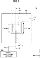
- FIG. 1 is a plan view illustrating an antenna device 10 according to the embodiment.
- the antenna device 10 has a square shape in a plan view as seen from a front surface side (the positive side of the Y axis).
- a conductor layer 11 in a thin film shape made of a conductive material is formed over the entire surface of the antenna device 10.
- the antenna device 10 is provided on a vertical surface (for example, an outer circumferential surface of a vertically installed pillar). Therefore, in the present embodiment, the direction of a vertical edge of the antenna device 10 (Z axis direction) is defined as a vertical direction and an up-and-down direction, and the direction of a horizontal edge of the antenna device 10 (X axis direction) is defined as a horizontal direction and a left-and-right direction. Furthermore, in the present embodiment, a direction normal to the surface of the antenna device 10 (i.e., a direction orthogonal to the XZ plane) is defined as a Y axis direction. In the present embodiment, the positive side of the Y axis of the antenna device 10 is referred to as a front side, and the negative side of the Y axis of the antenna device 10 is referred to as a rear side.
- an antenna element 5 in a slit shape that has a belt shape and a square shape is provided in a central portion of the conductor layer 11 of the antenna device 10.
- the antenna element 5 is what is termed as a slot loop antenna.
- the antenna element 5 is formed by cutting out a portion of the conductor layer 11.
- the antenna element 5 is used for transmitting and receiving electromagnetic waves in a predetermined frequency band.
- the antenna element 5 is used for transmitting and receiving electromagnetic waves in a frequency band lower than 6 GHz (for example, 3.7 GHz band or 4.5 GHz band) referred to as "Sub 6 " used in 5G (fifth generation mobile communication system), but applicable frequencies are not limited thereto.
- the antenna element 5 has a square shape with its vertical edge being in the vertical direction and its horizontal edge being in the horizontal direction in a plan view as seen from the front side (the positive side of the Y axis).
- a portion on the inner side of the antenna element 5 functions as a ground plate 9A, and a portion on the outer side of the antenna element 5 functions as a ground plate 9B.
- a feeding line 3 in a thin film shape and in a belt shape, that is made of a conductive material is provided on the rear side (the negative side of the Y axis) of the conductor layer 11.
- the feeding line 3 linearly extends upward (i.e., in the Z axis positive direction) from the central portion, in the horizontal direction (X axis direction), of the lower edge portion of the antenna device 10.
- the upper end portion of the feeding line 3 is connected to the vicinity of the lower edge portion of the ground plate 9A through a via 4.
- the feeding line 3 may be open at a position that is away by a distance of about 1/4 ⁇ g (where ⁇ g is the electrical length of one wavelength in view of the effect of the dielectric constant of the flexible substrate 12) from the lower edge portion of the ground plate 9A, so that the feeding line 3 is electrically connected to the ground plate 9A in a non-contact manner by electromagnetic coupling.
- a signal processing circuit 20 is connected to a connection point 3A provided at the lower end portion of the feeding line 3 via a connection line 21.
- the signal processing circuit 20 includes, for example, an AMP (Amplifier), a switch, a mixer, a DAC (Digital to Analog Converter), an ADC (Analog to Digital Converter), and the like.
- the antenna device 10 can radiate electromagnetic waves (vertically polarized waves) for carrying the signal in a predetermined frequency band from the antenna element 5.
- the signal processing circuit 20 may be provided outside of the antenna device 10 or may be provided in the antenna device 10 (for example, on a surface of the flexible substrate 12).
- the length of one edge of the square shape formed by the antenna element 5 is "15.00 mm", which is 1/4 wavelength of the predetermined frequency, and the length of one edge of the square shape formed by the ground plate 9A is "12.00 mm”. That is, the width of the belt of the antenna element 5 is "1.50 mm”.
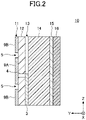
- FIG. 2 is a cross-sectional view taken along line A-A of the antenna device 10 according to the embodiment.
- the antenna device 10 includes a conductor layer 11, a flexible substrate 12, a wiring layer 13, a dielectric 14, a reflector plate 15, and a flexible substrate 16, which are arranged from the front surface side (the positive side of the Y axis).
- the antenna device 10 has a multilayer structure formed by stacking multiple constituent members.
- the antenna device 10 is not limited to the cross-sectional configuration of FIG.
- the wiring layer 13 may be formed on the front surface of the flexible substrate 12 (the surface on the positive side of the Y axis), and the conductor layer 11 may be formed on the rear surface of the flexible substrate 12 (the surface on the negative side of the Y axis).
- the reflector plate 15 may be formed on the rear surface of the flexible substrate 16 (the surface on the negative side of the Y axis).
- the reflector plate 15 may be provided at least on the rear side (the negative side of the Y axis) with respect to the dielectric 14, and for example, the reflector plate 15 may be formed on the rear surface of the dielectric 14 (the surface on the negative side of the Y axis) .
- the antenna device 10 does not have to have the flexible substrate 16.
- the conductor layer 11 is formed on the front surface of the flexible substrate 12 (the surface on the positive side of the Y axis) .
- the conductor layer 11 is in a thin film shape and has conductivity.
- the conductor layer 11 is made of a conductive material such as copper.
- the thickness of the conductor layer 11 is 1 nm to 32 ⁇ m.
- the antenna element 5 in the belt shape is formed in a square shape.
- the antenna element 5 is formed by partially cutting out a portion of the conductor layer 11.
- the ground plate 9A in the square shape is formed in an area surrounded by the antenna element 5.
- the conductor layer 11 is formed over the entire surface of the flexible substrate 12. That is, in the example illustrated in FIG. 1 , the conductor layer 11 is in a square shape similar to the flexible substrate 12 in a plan view.
- the flexible substrate 12 is a member that is made of resin and that is in a thin film shape having flexibility.
- the flexible substrate 12 is formed using a resin material having flexibility such as fluorine, COP (cyclo olefin polymer), PET (polyethylene terephthalate), PEN (polyethylene naphthalate), polyimide, Peek (polyether ether ketone), LCP (liquid crystal polymer), or other composite materials.
- the thickness of the flexible substrate 16 is 1 ⁇ m to 300 ⁇ m.
- the flexible substrate 12 is provided with the via 4 penetrating the flexible substrate 12 in the up-and-down direction.
- the wiring layer 13 is formed on the rear surface of the flexible substrate 12 (the surface on the negative side of the Y axis).
- the wiring layer 13 is provided with the feeding line 3 in a thin film shape and in a belt shape that linearly extends in the up-and-down direction (Z axis direction).
- the upper end portion of the feeding line 3 is connected to the lower edge portion of the ground plate 9A to be orthogonal thereto through the via 4 provided in the flexible substrate 12.
- the antenna element 5 can radiate vertically polarized waves.
- the dielectric 14 is a bendable plate-shaped member having flexibility that is provided on the rear side of the flexible substrate 12.
- the dielectric 14 is made of an elastic dielectric material (for example, sponge, rubber, urethane, and the like).
- the dielectric 14 has such a thickness as to achieve a predetermined bandwidth in a predetermined frequency band.
- a suitable thickness of the dielectric 14 may be determined by simulation or the like.
- the dielectric 14 is bonded to the rear surface (the surface on the negative side of the Y axis) of the flexible substrate 12 by any bonding means (for example, adhesives, double-sided tapes, and the like).
- the shape and size of the dielectric 14 are the same as the shape and size of the flexible substrate 12, but the present embodiment is not limited thereto.
- the dielectric 14 may have a larger size than the flexible substrate 12 and may have a shape different from the flexible substrate 12 (that is, a shape different from a square shape).
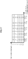
- FIGs. 17 and 18 are diagrams illustrating examples of bandwidths based on combinations of the thicknesses and dielectric constants of dielectric 14 in the antenna device 10 according to the embodiment (the antenna device 10 having the configurations illustrated in FIGs. 1 and 2 ).
- FIG. 17 illustrates an example of a bandwidth in which the VSWR is less than 1.5.
- FIG. 18 illustrates an example of a bandwidth in which the VSWR is less than 2.0.
- the bandwidth of the antenna system 10 may be determined based on a combination of the thickness and the dielectric constant of the dielectric 14. Therefore, in order to achieve a suitable bandwidth (that is, a sufficiently wide bandwidth) with the antenna device 10, it is preferable to derive the lists illustrated in FIGs. 17 and 18 in advance by simulation or the like, and to determine the thickness and dielectric constant of the dielectric 14 that is actually used based on the list.
- the dielectric constant of the dielectric 14 can be changed, for example, by adjusting and changing the material.
- the bandwidth in which the VSWR is less than 1.5 is preferably 2% or more, more preferably 3% or more, and still more preferably 5% or more.
- the bandwidth for which the VSWR is less than 2.0 is preferably 3.5% or more, more preferably 7% or more, and still more preferably 10.5% or more.
- the antenna device 10 according to the embodiment is configured to be bendable and to have the dielectric 14, and thus, a sufficiently wide bandwidth can be achieved overall as compared with conventional bendable antenna devices. Furthermore, it has been confirmed that even when the antenna device 10 according to the embodiment is used in a bent state, a change in the bandwidth hardly occurs as compared with the case where it is used in a flat state.
- the reflector plate 15 is formed over the entire front surface (the surface on the positive side of the Y axis) of the flexible substrate 16.
- the reflector plate 15 is in a thin film shape and has conductivity.
- the reflector plate 15 is made of a conductive material such as copper.
- the thickness of the reflector plate 15 is 1 nm to 32 ⁇ m.
- the reflector plate 15 is provided to reflect radiation of electromagnetic waves from the antenna element 5 to the rear side (the negative side of the Y axis) of the antenna device 10.
- the flexible substrate 16 is provided so as to be stacked on the rear surface (the surface on the negative side of the Y axis) of the dielectric 14. Similar to the flexible substrate 12, the flexible substrate 16 is a member that is made of resin and that is in a thin film shape having flexibility. For example, the flexible substrate 16 is formed by using substantially the same material as the flexible substrate 12. However, the flexible substrate 16 may be different from the flexible substrate 12 in at least one of material and thickness.
- the flexible substrate 16 is bonded to the rear surface (the surface on the negative side of the Y axis) of the dielectric 14 by any bonding means (for example, adhesives, double-sided tapes, and the like) with the reflector plate 15 being formed on the front surface (the surface on the positive side of the Y axis).
- any bonding means for example, adhesives, double-sided tapes, and the like
- FIG. 3 is a drawing illustrating an example of installation of the antenna device 10 according to the embodiment to an outer circumferential surface 70A of a pillar 70.
- the antenna device 10 can be bent as a whole because the dielectric 14 and the flexible substrates 12, 16 are bendable. Therefore, illustrated in FIG. 3 , the antenna device 10 is installableon the outer circumferential surface 70A while it is bent along the outer circumferential surface 70A of the pillar 70.
- the antenna device 10 is installableon the outer circumferential surface 70A of the pillar 70, such as a traffic signal, a street lamp, a telephone pole, and the like, but is not limited thereto.
- the antenna device 10 can be fixed to the outer circumferential surface 70A of the pillar 70 by any bonding means (for example, adhesives, double-sided tapes, and the like).
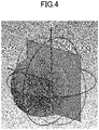
- FIG. 4 and FIG. 5 are drawings illustrating directivities of the antenna device 10 according to the embodiment.
- FIG. 5 (a) illustrates the directivity of the antenna device 10 in the ZY plane in 4.85 GHz band.
- FIG 5(b) illustrates the directivity of the antenna device 10 in the XY plane in the 4.85 GHz band.
- a solid line represents the directivity when the antenna device 10 is provided with the reflector plate 15, and a broken line represents the directivity when the antenna device 10 is not provided with the reflector plate 15.
- the antenna device 10 can radiate, with the antenna element 5, vertically polarized waves with a sufficiently high gain in the front surface direction of the antenna device 10 (the positive side of the Y axis).
- the antenna device 10 according to the embodiment can reflect, with the reflector plate 15, vertically polarized waves emitted in the rear surface direction of the antenna device 10 (the negative side of the Y axis) toward the front surface direction of the antenna device 10 (the positive side of the Y axis). Therefore, the antenna device 10 according to the embodiment can enhance the strength of the vertically polarized electromagnetic waves toward the front surface direction of the antenna device 10 (the positive side of the Y axis) .
- the antenna device 10 according to the embodiment can reduce the effect of the outer circumferential surface 70A, which is an object to which the antenna device 10 is to be installed, on the electromagnetic waves radiated from the antenna element 5 by providing the reflector plate 15. That is, the antenna device 10 according to the embodiment is installableon various outer circumferential surfaces 70A irrespective of the material of the outer circumferential surface 70A.
- FIG. 6 is a graph illustrating antenna characteristics (S11) of the antenna device 10 according to the embodiment.
- the antenna device 10 according to the embodiment can reduce the reflection coefficient (S11) to "-10 dB" or less (corresponding to VSWR ⁇ 2) in a predetermined frequency band (4.75 to 4.95 GHz) by providing the dielectric 14 having a certain thickness (15 mm in this test) and by providing the reflector plate 15. That is, the antenna device 10 according to the embodiment can achieve a wide bandwidth (200 MHz) in the predetermined frequency band (4.75 to 4.95 GHz).
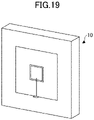
- FIG. 19 is an external perspective view illustrating a first use state of the antenna device 10 according to the embodiment.
- FIG. 20 is a graph illustrating antenna characteristics (VSWR value) in the first use state of the antenna device 10 according to the embodiment.
- the antenna device 10 according to the embodiment can be used in a flat state as the first use state. This first use state is effective when the antenna device 10 is installed on a flat installation target surface.
- the antenna device 10 according to the embodiment can achieve a wide bandwidth having a center frequency of 3.8 GHz in the first use state, and in particular, can achieve a sufficiently wide bandwidth of "4.1%" as a bandwidth having a VSWR of less than 1.5.
- FIG. 21 is an external perspective view illustrating a second use state of the antenna device 10 according to the embodiment.
- FIG. 22 is a graph illustrating antenna characteristics (VSWR value) in the second use state of the antenna device 10 according to the embodiment.
- the antenna device 10 according to the embodiment can be used in a bent state that is bent along the horizontal direction as the second use state. This second use state is effective when the antenna device 10 is installed on an installation target surface that is bent along the horizontal direction (for example, the outer circumferential surface of a cylindrical pillar or the like) .
- an installation target surface for example, the outer circumferential surface of a cylindrical pillar or the like
- the antenna device 10 according to the embodiment can achieve a wide bandwidth having a center frequency of 3.8 GHz in the second use state, and in particular, can achieve a sufficiently wide bandwidth of "2.5%" as a bandwidth having a VSWR of less than 1.5.
- FIG. 23 is an external perspective view illustrating a third use state of the antenna device 10 according to the embodiment.
- FIG. 24 is a graph illustrating antenna characteristics (VSWR value) in the third use state of the antenna device 10 according to the embodiment.
- the antenna device 10 according to the embodiment can be used in a bent state that is bent along the vertical direction as the third use state. This third state of use is effective when the antenna device 10 is installed on an installation target surface that is bent along the vertical direction.
- FIG. 24 is a graph illustrating antenna characteristics (VSWR value) in the third use state of the antenna device 10 according to the embodiment.
- the antenna device 10 according to the embodiment can be used in a bent state that is bent along the vertical direction as the third use state. This third state of use is effective when the antenna device 10 is installed on an installation target surface that is bent along the vertical direction.
- the antenna device 10 according to the embodiment can achieve a wide bandwidth having a center frequency of 3.8 GHz in the third use state, and in particular, can achieve a sufficiently wide bandwidth of "3.9%" as a bandwidth having a VSWR of less than 1.5.
- the same antenna device 10 having the configurations illustrated in FIGs. 1 and 2 is used, and the thickness of the dielectric 14 is "0.1875 * ⁇ g" and the dielectric constant of the dielectric 14 is "2".
- the antenna device 10 according to the embodiment has the configuration illustrated in FIGs. 1 and 2 , a sufficient wide bandwidth can be achieved when it is used in either the flat state or the bent state.
- FIG. 7 is a plan view illustrating an antenna device 10A according to a first modified embodiment.
- the antenna device 10A illustrated in FIG. 7 is different from the antenna device 10 illustrated in FIG. 1 in that the wiring layer 13 on the rear side (the negative side of the Y axis) of the conductor layer 11 is further provided with a feeding line 6 in a thin film shape and in belt shape that is made of a conductive material.
- the feeding line 6 linearly extends from the central portion of the left edge portion of the antenna device 10 toward the right (the negative side of the X axis) .
- the right end portion of the feeding line 6 is connected to the vicinity of the left edge portion of the ground plate 9A through a via 4.
- a signal processing circuit 20 is connected to a connection point 6A provided at the left end portion of the feeding line 6 via a connection line 22.
- the antenna device 10A according to the first modified embodiment can radiate vertically polarized waves and horizontally polarized waves from the antenna element 5. Specifically, when a signal is fed from the signal processing circuit 20 to the ground plate 9A via the connection line 21 and the feeding line 3 (a first feeding line), the antenna device 10A according to the first modified embodiment can radiate vertically polarized waves of the predetermined frequency band from the antenna element 5. Furthermore, when a signal is fed from the signal processing circuit 20 to the ground plate 9A via the connection line 22 and the feeding line 6 (a second feeding line), the antenna device 10A according to the first modified embodiment can radiate horizontally polarized waves of the predetermined frequency band from the antenna element 5.
- FIG. 8 is a drawing illustrating a directivity of the antenna device 10A according to the first modified embodiment.
- FIG. 8 (a) illustrates the directivity of the antenna device 10A according to the first modified embodiment in the ZY plane in 4.85 GHz band.
- FIG. 8 (b) illustrates the directivity of the antenna device 10A according to the first modified embodiment in the XY plane in the 4.85 GHz band.
- a solid line represents the antenna characteristics in the YZ plane of vertically polarized waves radiated from the antenna element 5, and a broken line represents the antenna characteristics in the YX plane of vertically polarized waves radiated from the antenna element 5.
- a solid line represents the antenna characteristics in the YZ plane of horizontally polarized waves radiated from the antenna element 5, and a broken line represents the antenna characteristics of the YX plane of horizontally polarized waves radiated from the antenna element 5.
- the antenna device 10A according to the first modified embodiment can radiate, with the antenna element 5, each of vertically polarized waves and horizontally polarized waves with a sufficiently high gain in the front surface direction of the antenna device 10A (the positive side of the Y axis).
- FIG. 8 (a) and 8 (b) illustrate the antenna characteristics when the antenna device 10A according to the first modified embodiment is not provided with the reflector plate 15.
- the electromagnetic waves in the front surface direction (the positive side of the Y axis) can be strengthened by reflecting the radiation of the vertically polarized waves and the horizontally polarized waves emitted in the rear surface direction of the antenna device 10A (the negative side of the Y axis).
- FIG. 9 is a graph illustrating the antenna characteristics (S11, S21) of the antenna device 10A according to the first modified embodiment.
- a solid line represents the reflection coefficient (S11) of each of the vertically polarized waves and horizontally polarized waves by the antenna device 10A
- a broken line represents the transmission coefficient (S21) of each of the vertically polarized waves and horizontally polarized waves by the antenna device 10A.
- the antenna device 10A according to the first modified embodiment can reduce the reflection coefficient (S11) of each of the vertically polarized waves and horizontally polarized waves to "-10 dB" or less (corresponding to VSWR ⁇ 2) in the predetermined frequency band (4.75 to 4.95 GHz) by providing the antenna device 10A according to the first modified embodiment with the dielectric 14 having a certain thickness (15 mm in this test) and with the reflector plate 15.
- the antenna device 10A according to the first modified embodiment can reduce the transmission coefficient (S21) of each of the vertically polarized waves and horizontally polarized waves to "-15 dB" or less in the predetermined frequency band (4.75 to 4.95 GHz)
- the antenna device 10 can achieve a wide bandwidth (200 MHz) in the predetermined frequency band (4.75 to 4.95 GHz).
- FIG. 10 is a plan view illustrating an antenna device 10B according to the second modified embodiment.
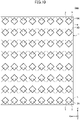
- the antenna device 10B illustrated in FIG. 10 includes a plurality of antenna elements 5 arranged in a matrix form arranged in the horizontal direction (X axis direction) and the vertical direction (Z axis direction) in the conductor layer 11.
- the antenna device 10B has eight antenna elements 5 arranged side by side in the horizontal direction (X axis direction) and in the vertical direction (Z axis direction). That is, the antenna device 10B has 64 antenna elements 5 arranged in the 8 by 8 matrix form in the conductor layer 11.
- two feeding lines 3, 6 of which the directions are 90 degrees different from each other are provided for each of the 64 antenna elements 5, similarly to the antenna device 10A illustrated in FIG. 7 .
- the multiple antenna elements 5 and the feeding lines 3, 6 in the lower four rows are rotated counterclockwise by 45 degrees as compared with the antenna elements 5 and the feeding lines 3, 6 of the antenna device 10A illustrated in FIG. 7 .
- the feeding line 3 is connected at a right angle to the lower right oblique edge of the ground plate 9A in the antenna element 5, and the feeding line 6 is connected at a right angle to the lower left oblique edge of the ground plate 9A.
- the multiple antenna elements 5 and the feeding lines 3, 6 in the upper four rows are inverted upside down as compared with the antenna elements 5 and the feeding lines 3, 6 in the lower four rows.
- the feeding line 3 is connected at a right angle to the upper right oblique edge of the ground plate 9A
- the feeding line 6 is connected at a right angle to the upper left oblique edge of the ground plate 9A.
- the antenna device 10B configured as described above can radiate two kinds of electromagnetic waves having polarization directions 90 degrees different from each other from each of the multiple antenna elements 5.
- FIG. 11 is a drawing illustrating an example of connection of the feeding lines 3, 6 in the antenna device 10B according to the second modified embodiment.
- FIG. 11 illustrates lower four antenna elements 5 arranged in the vertical direction in the antenna device 10B.
- the antenna device 10B includes two feeding lines 3-1, 3-2 and two feeding lines 6-1, 6-2 for the four antenna elements 5.
- the feeding lines 3-1, 6-1 are connected to the lower two antenna elements 5.
- the feeding lines 3-2, 6-2 are connected to the upper two antenna elements 5.
- Each of the feeding lines 3-1, 3-2, 6-1, and 6-2 is connected to the signal processing circuit 20.
- the antenna device 10B configured as described above can radiate two kinds of electromagnetic waves having polarization directions 90 degrees different from each other from the lower two antenna elements 5 of the four antenna elements 5.
- the antenna device 10B When power is fed from the signal processing circuit 20 to either the feeding line 3-2 or the feeding line 6-2, the antenna device 10B can radiate two kinds of electromagnetic waves having polarization directions 90 degrees different from each other from the upper two antenna elements 5 of the four antenna elements 5.
- the antenna device 10B When the antenna device 10B is disposed on the outer circumferential surface 70A of the pillar 70 in a cylindrical shape, the antenna device 10B radiates two kinds of electromagnetic waves having polarization directions 90 degrees different from each other in each of multiple directions (up to 8 directions) around the pillar 70. In this case, the antenna device 10B can more reliably transmit electromagnetic waves in each of multiple directions (up to 8 directions) around the pillar 70.
- the antenna device 10B can individually drive each of the 64 antenna elements 5 as required, that is, the antenna device 10B can radiate electromagnetic waves in only one or more particular directions.
- the antenna device 10B can radiate electromagnetic waves in multiple particular directions simultaneously or with a time difference.
- the antenna device 10B can transmit multiple different kinds of signals to multiple particular directions simultaneously or with a time difference.
- the antenna device 10B can be used for multiple-input and multiple-output (MIMO), beamforming, and the like.
- MIMO multiple-input and multiple-output
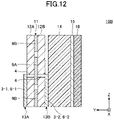
- FIG. 12 is a drawing illustrating a cross-sectional configuration of the antenna device 10B according to the second modified embodiment.
- the antenna device 10B according to the second modified embodiment includes a first wiring layer 13A, a first flexible substrate 12A, a conductor layer 11, a second flexible substrate 12B, a second wiring layer 13B, a dielectric 14, a reflector plate 15, and a flexible substrate 16, which are arranged from the front surface side (the positive side of the Y axis) .
- the reflector plate 15 may be provided at least on the rear side (the negative side of the Y axis) with respect to the dielectric 14, and for example, the reflector plate 15 may be formed on the rear surface of the dielectric 14 (the surface on the negative side of the Y axis). In this case, the antenna device 10B does not have to have the flexible substrate 16.
- the antenna device 10B according to the second modified embodiment is provided with two flexible substrates 12A, 12B stacked on each other.
- the conductor layer 11 is provided between the two flexible substrates 12A, 12B.
- the first wiring layer 13A is provided on the front surface of the first flexible substrate 12A
- the second wiring layer 13B is provided on the rear surface of the second flexible substrate 12B.
- the first wiring layer 13A is provided with the feeding lines 3-1, 6-1 illustrated in FIG. 11 .
- the feeding lines 3-1, 6-1 are connected to the ground plate 9A provided in the conductor layer 11 through the via 4 penetrating the first flexible substrate 12A.
- the second wiring layer 13B is provided with the feeding lines 3-2, 6-2 illustrated in FIG. 11 .
- the feeding lines 3-2, 6-2 are connected to the ground plate 9A provided in the conductor layer 11 through the via 4 penetrating the second flexible substrate 12B.
- the antenna device 10B according to the second modified embodiment includes the first wiring layer 13A and the second wiring layer 13B, so that the multiple feeding lines can be distributed to the first wiring layer 13A and the second wiring layer 13B.
- the antenna device 10B according to the second modified embodiment can reduce the number of wirings in each of the wiring layers 13A and 13B, and therefore, the degree of flexibility of wirings in the wiring layers 13A and 13B can be increased.
- FIG. 13 is a plan view illustrating an antenna device 10C according to the third modified embodiment.
- the antenna device 10C illustrated in FIG. 13 includes a dipole antenna ANT1, a dipole antenna ANT2, a feeding line 3, and a ground plate 9.
- the ground plate 9 includes a base portion 9a having a vertically long rectangular shape, a branch portion 9b branching to the left side from the left edge portion of the base portion 9a, and a branch portion 9c branching to the right side from the right edge portion of the base portion 9a.
- the feeding line 3 is provided in a layer closer to the front surface than is the ground plate 9, and is provided on the ground plate 9.
- the feeding line 3 includes: a straight line portion 3a extending linearly upward from the lower edge portion of the antenna device 10C at the central portion of the antenna device 10C in the horizontal direction (X axis direction); a branch portion 3b branching to the left side from the upper end portion of the straight line portion 3a; and a branch portion 3c branching to the right side from the upper end portion of the straight line portion 3a.
- the dipole antenna ANT1 includes, on the left side of the ground plate 9, an antenna element 5A extending linearly upward, and an antenna element 5B extending linearly downward.
- the lower end portion of the antenna element 5A is connected to the left end portion of the branch portion 9b of the ground plate 9.
- the upper end portion of the antenna element 5B is connected to the left end portion of the branch portion 3b of the feeding line 3.
- the dipole antenna ANT2 includes, on the right side of the ground plate 9, an antenna element 5C extending linearly upward, and an antenna element 5D extending linearly downward.
- the lower end portion of the antenna element 5C is connected to the right end portion of the branch portion 9c of the ground plate 9.
- the upper end portion of the antenna element 5D is connected to the right end portion of the branch portion 3c of the feeding line 3.
- the ground plate 9, the antenna element 5A, and the antenna element 5C are formed on the rear surface of the flexible substrate 12 (see FIG. 12 ). Furthermore, in the antenna device 10C, the feeding line 3, the antenna element 5B, and the antenna element 5D are formed on the front surface of the flexible substrate 12.
- the antenna device 10C configured as described above can radiate vertically polarized waves in a predetermined frequency band from each of the dipole antennas ANT1, ANT2.
- FIG. 14 is a plan view illustrating an antenna device 10D according to the fourth modified embodiment.
- the antenna device 10D illustrated in FIG. 14 includes a dipole antenna ANT3, a feeding line 3, and a ground plate 9.
- the ground plate 9 has a vertically long rectangular shape.
- the dipole antenna ANT3 and the feeding line 3 are provided in a layer closer to the front surface than is the ground plate 9.
- the feeding line 3 includes: a straight line portion 3a extending linearly in the up-and-down direction; a branch portion 3b branching to the left side from the upper end portion of the straight line portion 3a; and a branch portion 3c branching to the right side from the upper end portion of the straight line portion 3a.
- the dipole antenna ANT3 includes, on the front side with respect to the ground plate 9, an antenna element 5E extending linearly to the left side from the upper end portion of the branch portion 3b of the feeding line 3, and an antenna element 5F extending linearly to the right side from the upper end portion of the branch portion 3c of the feeding line 3.
- the ground plate 9 is formed on the rear surface of the flexible substrate 12 (see FIG. 12 ). Furthermore, in the antenna device 10D, the feeding line 3, the antenna element 5E, and the antenna element 5F are formed on the front surface of the flexible substrate 12.
- the antenna device 10D configured as described above can radiate horizontally polarized waves in a predetermined frequency band from the dipole antenna ANT3.
- FIG. 15 is a plan view illustrating an antenna device 10E according to the fifth modified embodiment.
- the antenna device 10E illustrated in FIG. 15 includes an antenna element 5H and a feeding line 3.
- an antenna element 5H in a belt shape and in a slit shape that linearly extends in the horizontal direction (X axis direction) is provided in the central portion, in the vertical direction (Z axis direction), of the conductor layer 11 of the antenna device 10E.
- the antenna element 5H is what is termed as a slot antenna.
- the antenna element 5H is formed by cutting out a portion of the conductor layer 11. In the conductor layer 11 of the antenna device 10E, a portion on the outer side of the antenna element 5H functions as the ground plate 9.
- the feeding line 3 linearly extends upward from the lower edge portion of the antenna device 10E at the central portion of the antenna device 10E in the horizontal direction (X axis direction) .
- the feeding line 3 is open at a position of the ground plate 9 that is away by a distance of about 1/4 ⁇ g (where ⁇ g is the electrical length of one wavelength in view of the effect of the dielectric constant of the flexible substrate 12) from the upper edge portion of the antenna element 5H, so that the feeding line 3 is electrically connected to the antenna element 5H in a non-contact manner by electromagnetic coupling. Therefore, the antenna element 5H can radiate vertically polarized waves.
- the antenna device 10E configured as described above can radiate vertically polarized waves in the predetermined frequency band from the antenna element 5H.
- FIG. 16 is a plan view illustrating an antenna device according 10F to the sixth modified embodiment.
- the antenna device 10F illustrated in FIG. 16 further includes an antenna element 51 and a feeding line 6, as compared with the antenna device 10E illustrated in FIG. 15 .
- the antenna element 51 is in a belt shape and in a slit shape.
- the antenna element 51 linearly extends in the vertical direction (Z axis direction) at the central portion in the horizontal direction (X axis direction) of the conductor layer 11 of the antenna device 10F.
- the antenna element 51 is orthogonal to the antenna element 5H.
- the feeding line 3 is provided, on the front side of the conductor layer 11, to extend linearly upward from the lower edge portion of the antenna device 10E.
- the upper end portion of the feeding line 3 is open at a position of the ground plate 9 that is away by a distance of about 1/4 ⁇ g (where ⁇ g is the electrical length of one wavelength in view of the effect of the dielectric constant of the flexible substrate 12) from the upper edge portion of the antenna element 5H, so that the feeding line 3 is electrically connected to the antenna element 5H in a non-contact manner by electromagnetic coupling. Therefore, the antenna element 5H can radiate vertically polarized waves.
- the feeding line 6 is provided, on the rear side of the conductor layer 11, to extend linearly to the left side from the right edge portion of the antenna device 10E.
- the left end portion of the feeding line 6 is open at a position of the ground plate 9 that is away by a distance of about 1/4 ⁇ g (where ⁇ g is the electrical length of one wavelength in view of the effect of the dielectric constant of the flexible substrate 12) from the left edge portion of the antenna element 51, so that the feeding line 6 is electrically connected to the antenna element 51 in a non-contact manner by electromagnetic coupling. Therefore, the antenna element 51 can radiate horizontally polarized waves.
- the conductor layer 11 is provided between the two flexible substrates 12A, 12B. Furthermore, in the antenna device 10F, the feeding line 3 is provided on the front surface of the first flexible substrate 12A, and is electrically connected to the antenna element 5H in a non-contact manner by electromagnetic coupling. In the antenna device 10F, the feeding line 6 is provided on the rear surface of the second flexible substrate 12B, and is electrically connected to the antenna element 51 in a non-contact manner by electromagnetic coupling.
- the antenna device 10F configured as described above can radiate vertically polarized waves in the predetermined frequency band from the antenna element 5H.
- the antenna device 10F configured as described above can radiate horizontally polarized waves in the predetermined frequency band from the antenna element 51.
- each of the antenna devices 10B to 10F has the dielectric 14 having a certain thickness and the reflector plate 15. Therefore, any of the antenna devices 10B to 10F is installablealong the curved surface, can achieve a wide bandwidth in a predetermined frequency band, and can enhance radiation in the front surface direction by reflecting the radiation of electromagnetic waves in the rear surface direction.
- FIG. 25 is an external perspective view illustrating a flat state of an antenna device 10G according to the seventh modified embodiment.
- the antenna device 10G according to the seventh modified embodiment has a horizontally long rectangular shape in a plan view as seen from the front surface side (the positive side in the Z axis) .
- the antenna device 10G according to the seventh modified embodiment includes four antenna elements 5 arranged side by side of the X axis direction in the conductor layer 11.
- Each of the antenna elements 5 is the same as the antenna element 5 illustrated in FIGs. 1 and 2 , that is, has a belt shape and a square shape. Similarly to the antenna element 5 illustrated in FIGs.
- the antenna device 10G according to the seventh modified embodiment is the same as that of the antenna device 10 illustrated in FIGs. 1 and 2 .
- the arrangement interval of two adjacent antenna elements is 0.5 ⁇ .
- the thickness of the dielectric 14 is "0.1875 * ⁇ " and the dielectric constant of the dielectric 14 is" 2".
- the antenna device 10G according to the seventh modified embodiment can be used in a flat state parallel to the XY plane.
- FIG. 26 is a drawing illustrating a directivity of the antenna device 10G according to the seventh modified embodiment (a flat state illustrated in FIG. 25 ).
- FIG. 26 (a) illustrates the antenna characteristics in the ZX plane in a predetermined frequency band of the antenna device 10G according to the seventh modified embodiment.
- FIG. 26 (b) illustrates the antenna characteristics in the YZ plane in the predetermined frequency band of the antenna device 10G according to the seventh modified embodiment.
- the antenna device 10 according to the embodiment can radiate electromagnetic waves with a sufficiently high gain (12.4 dBi) in a particular direction even when multiple antenna elements 5 are arrayed.
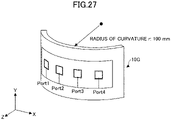
- FIG. 27 is an external perspective view illustrating a bent state of the antenna device 10G according to the seventh modified embodiment.
- the antenna device 10G according to the seventh modified embodiment can also be used in a bent state with respect to the XY plane.
- the radius of curvature of the antenna device 10G is 100 mm.
- FIG. 28 is a drawing illustrating a directivity of the antenna device 10G according to the seventh modified embodiment (a bent state illustrated in FIG. 27 ).
- FIG. 28 (a) illustrates the antenna characteristics in the ZX plane in a predetermined frequency band of the antenna device 10G according to the seventh modified embodiment.
- FIG. 28 (b) illustrates the antenna characteristics in the YZ plane in the predetermined frequency band of the antenna device 10G according to the seventh modified embodiment.
- the antenna device 10 according to the embodiment can radiate electromagnetic waves with a sufficiently high gain (11.1 dBi) in a particular direction, without appreciable change from the case of the flat state.
- the configuration illustrated in the above embodiment shows an example of the contents of the present disclosure, and may be combined with other known techniques, or a part of the configuration may be omitted or changed without departing from the gist of the present disclosure.
Landscapes
- Details Of Aerials (AREA)
- Aerials With Secondary Devices (AREA)
Abstract
Description
- The present disclosure relates to an antenna device.
- In recent years, there is an ongoing trend of expansion of services using high-speed and large-capacity wireless communication systems communicating in microwave and millimeter wave frequency bands, such as a trend of transition from 4G LTE to 5G (sub6). As an antenna used in such a frequency band, a patch antenna using a rigid substrate that is generally referred to as a CCL is known.
- The antenna device of
Patent Literature 1 can emit beams in multiple directions with a simpler structure as compared with the case where a flexible substrate having different thicknesses depending on the areas is used and a rigid substrate such as an LTCC substrate is connected to the flexible substrate. - PTL 1:
Japanese Laid-Open Patent Publication No. 2019-4241 - According to tests conducted by the inventors of the present invention, it has been found that, in an antenna device such as a patch antenna used in a frequency band lower than 6 GHz that is referred to as "Sub6" (for example, 3.7 GHz band or 4.5 GHz band), in order to ensure a wide bandwidth in a predetermined frequency band, it is preferable that the substrate constituting the patch antenna has a sufficient thickness, for example, in the case of a glass substrate, the thickness is preferably 6 mm or more.
- However, with the conventional technique, as the thickness of the glass substrate or the resin substrate increases, it becomes difficult to bend the antenna device, and therefore, it becomes difficult to install the antenna device on a curved surface (for example, an outer circumferential surface of a cylindrical object).
- The present disclosure has been made in view of the above, and it is an object of the present disclosure to provide an antenna device that is installablealong a curved surface, can achieve a wide bandwidth in a predetermined frequency band, and can emit strong electromagnetic waves in a single direction by reflecting the radiation of electromagnetic waves in the rear surface direction.
- In order to solve the above-described problem and achieve the object, an antenna device according to the present disclosure includes a flexible substrate, an antenna element provided on a front surface or a rear surface of the flexible substrate, a feeding line provided on the front surface or the rear surface of the flexible substrate to feed power to the antenna element, a dielectric in a plate shape stacked on a rear side of the flexible substrate, the dielectric having flexibility and being bendable, and a reflector plate provided on a rear side of the dielectric.
- According to the antenna device of the present disclosure, an antenna device that is installablealong a curved surface, can achieve a wide bandwidth in a predetermined frequency band, and can emit strong electromagnetic waves in a single direction by reflecting the radiation of electromagnetic waves in the rear surface direction can be provided.
-
-
FIG. 1 is a plan view illustrating an antenna device according to the embodiment. -
FIG. 2 is a cross-sectional view taken along line A-A of the antenna device according to the embodiment. -
FIG. 3 is a drawing illustrating an example of installation of the antenna device according to the embodiment to an outer circumferential surface of a pillar. -
FIG. 4 illustrates a directivity of the antenna device according to the embodiment. -
FIG. 5 illustrates a directivity of the antenna device according to the embodiment. -
FIG. 6 is a graph illustrating antenna characteristics (S11) of the antenna device according to the embodiment. -
FIG. 7 is a plan view illustrating an antenna device according to a first modified embodiment. -
FIG. 8 is a drawing illustrating a directivity of the antenna device according to the first modified embodiment. -
FIG. 9 is a graph illustrating antenna characteristics (S11, S21) of the antenna device according to the first modified embodiment. -
FIG. 10 is a plan view illustrating an antenna device according to a second modified embodiment. -
FIG. 11 is a drawing illustrating an example of connection of feeding lines of the antenna device according to the second modified embodiment. -
FIG. 12 is a drawing illustrating a cross-sectional configuration of an antenna device according to a second modified embodiment. -
FIG. 13 is a plan view illustrating an antenna device according to a third modified embodiment. -
FIG. 14 is a plan view illustrating an antenna device according to a fourth modified embodiment. -
FIG. 15 is a plan view illustrating an antenna device according to a fifth modified embodiment. -
FIG. 16 is a plan view illustrating an antenna device according to a sixth modified embodiment. -
FIG. 17 is a diagram illustrating an example of bandwidths based on combinations of the thickness and the dielectric constant of dielectric in the antenna device according to the embodiment. -
FIG. 18 is a diagram illustrating an example of bandwidths based on combinations of the thickness and the dielectric constant of dielectric in the antenna device according to the embodiment. -
FIG. 19 is an external perspective view illustrating a first use state of the antenna device according to the embodiment. -
FIG. 20 is a graph illustrating antenna characteristics (VSWR value) in a first use state of the antenna device according to the embodiment. -
FIG. 21 is an external perspective view illustrating a second use state of the antenna device according to the embodiment. -
FIG. 22 is a graph illustrating antenna characteristics (VSWR value) in the second use state of the antenna device according to the embodiment. -
FIG. 23 is an external perspective view illustrating a third use state of the antenna device according to the embodiment. -
FIG. 24 is a graph illustrating antenna characteristics (VSWR value) in the third use state of the antenna device according to the embodiment. -
FIG. 25 is an external perspective view illustrating a flat state of an antenna device according to a seventh modified embodiment. -
FIG. 26 is a drawing illustrating a directivity of the antenna device according to the seventh modified embodiment (a flat state illustrated inFIG. 25 ). -
FIG. 27 is an external perspective view illustrating a bent state of the antenna device according to the seventh modified embodiment. -
FIG. 28 is a drawing illustrating a directivity of the antenna device according to the seventh modified embodiment (a bent state illustrated inFIG. 27 ). - Embodiments according to the present disclosure are described below with reference to the drawings.
-
FIG. 1 is a plan view illustrating anantenna device 10 according to the embodiment. As illustrated inFIG. 1 , theantenna device 10 has a square shape in a plan view as seen from a front surface side (the positive side of the Y axis). As illustrated inFIG. 1 , aconductor layer 11 in a thin film shape made of a conductive material is formed over the entire surface of theantenna device 10. - In the present embodiment, the
antenna device 10 is provided on a vertical surface (for example, an outer circumferential surface of a vertically installed pillar). Therefore, in the present embodiment, the direction of a vertical edge of the antenna device 10 (Z axis direction) is defined as a vertical direction and an up-and-down direction, and the direction of a horizontal edge of the antenna device 10 (X axis direction) is defined as a horizontal direction and a left-and-right direction. Furthermore, in the present embodiment, a direction normal to the surface of the antenna device 10 (i.e., a direction orthogonal to the XZ plane) is defined as a Y axis direction. In the present embodiment, the positive side of the Y axis of theantenna device 10 is referred to as a front side, and the negative side of the Y axis of theantenna device 10 is referred to as a rear side. - In the example illustrated in
FIG. 1 , anantenna element 5 in a slit shape that has a belt shape and a square shape is provided in a central portion of theconductor layer 11 of theantenna device 10. Theantenna element 5 is what is termed as a slot loop antenna. Theantenna element 5 is formed by cutting out a portion of theconductor layer 11. Theantenna element 5 is used for transmitting and receiving electromagnetic waves in a predetermined frequency band. For example, theantenna element 5 is used for transmitting and receiving electromagnetic waves in a frequency band lower than 6 GHz (for example, 3.7 GHz band or 4.5 GHz band) referred to as "Sub 6 " used in 5G (fifth generation mobile communication system), but applicable frequencies are not limited thereto. Theantenna element 5 has a square shape with its vertical edge being in the vertical direction and its horizontal edge being in the horizontal direction in a plan view as seen from the front side (the positive side of the Y axis). In theconductor layer 11, a portion on the inner side of theantenna element 5 functions as aground plate 9A, and a portion on the outer side of theantenna element 5 functions as aground plate 9B. - As illustrated in
FIG. 1 , in theantenna device 10, afeeding line 3, in a thin film shape and in a belt shape, that is made of a conductive material is provided on the rear side (the negative side of the Y axis) of theconductor layer 11. Thefeeding line 3 linearly extends upward (i.e., in the Z axis positive direction) from the central portion, in the horizontal direction (X axis direction), of the lower edge portion of theantenna device 10. The upper end portion of thefeeding line 3 is connected to the vicinity of the lower edge portion of theground plate 9A through avia 4. However, thefeeding line 3 may be open at a position that is away by a distance of about 1/4 λg (where λg is the electrical length of one wavelength in view of the effect of the dielectric constant of the flexible substrate 12) from the lower edge portion of theground plate 9A, so that thefeeding line 3 is electrically connected to theground plate 9A in a non-contact manner by electromagnetic coupling. Asignal processing circuit 20 is connected to aconnection point 3A provided at the lower end portion of thefeeding line 3 via aconnection line 21. Thesignal processing circuit 20 includes, for example, an AMP (Amplifier), a switch, a mixer, a DAC (Digital to Analog Converter), an ADC (Analog to Digital Converter), and the like. - By receiving a signal from the
signal processing circuit 20 to theground plate 9A via theconnection line 21 and thefeeding line 3, theantenna device 10 can radiate electromagnetic waves (vertically polarized waves) for carrying the signal in a predetermined frequency band from theantenna element 5. Thesignal processing circuit 20 may be provided outside of theantenna device 10 or may be provided in the antenna device 10 (for example, on a surface of the flexible substrate 12). - In the example illustrated in
FIG. 1 , the length of one edge of the square shape formed by theantenna element 5 is "15.00 mm", which is 1/4 wavelength of the predetermined frequency, and the length of one edge of the square shape formed by theground plate 9A is "12.00 mm". That is, the width of the belt of theantenna element 5 is "1.50 mm". -
FIG. 2 is a cross-sectional view taken along line A-A of theantenna device 10 according to the embodiment. As illustrated inFIG. 2 , theantenna device 10 includes aconductor layer 11, aflexible substrate 12, awiring layer 13, a dielectric 14, areflector plate 15, and aflexible substrate 16, which are arranged from the front surface side (the positive side of the Y axis). Theantenna device 10 has a multilayer structure formed by stacking multiple constituent members. Theantenna device 10 is not limited to the cross-sectional configuration ofFIG. 2 , and, for example, thewiring layer 13 may be formed on the front surface of the flexible substrate 12 (the surface on the positive side of the Y axis), and theconductor layer 11 may be formed on the rear surface of the flexible substrate 12 (the surface on the negative side of the Y axis). Also, for example, thereflector plate 15 may be formed on the rear surface of the flexible substrate 16 (the surface on the negative side of the Y axis). Also, thereflector plate 15 may be provided at least on the rear side (the negative side of the Y axis) with respect to the dielectric 14, and for example, thereflector plate 15 may be formed on the rear surface of the dielectric 14 (the surface on the negative side of the Y axis) . In this case, theantenna device 10 does not have to have theflexible substrate 16. - The
conductor layer 11 is formed on the front surface of the flexible substrate 12 (the surface on the positive side of the Y axis) . Theconductor layer 11 is in a thin film shape and has conductivity. For example, theconductor layer 11 is made of a conductive material such as copper. For example, the thickness of theconductor layer 11 is 1 nm to 32 µm. As illustrated inFIG. 1 , in theconductor layer 11, theantenna element 5 in the belt shape is formed in a square shape. Theantenna element 5 is formed by partially cutting out a portion of theconductor layer 11. Thus, in theconductor layer 11, theground plate 9A in the square shape is formed in an area surrounded by theantenna element 5. In the example illustrated inFIG. 1 , theconductor layer 11 is formed over the entire surface of theflexible substrate 12. That is, in the example illustrated inFIG. 1 , theconductor layer 11 is in a square shape similar to theflexible substrate 12 in a plan view. - The
flexible substrate 12 is a member that is made of resin and that is in a thin film shape having flexibility. For example, theflexible substrate 12 is formed using a resin material having flexibility such as fluorine, COP (cyclo olefin polymer), PET (polyethylene terephthalate), PEN (polyethylene naphthalate), polyimide, Peek (polyether ether ketone), LCP (liquid crystal polymer), or other composite materials. For example, the thickness of theflexible substrate 16 is 1 µm to 300 µm. Theflexible substrate 12 is provided with the via 4 penetrating theflexible substrate 12 in the up-and-down direction. - The
wiring layer 13 is formed on the rear surface of the flexible substrate 12 (the surface on the negative side of the Y axis). Thewiring layer 13 is provided with thefeeding line 3 in a thin film shape and in a belt shape that linearly extends in the up-and-down direction (Z axis direction). The upper end portion of thefeeding line 3 is connected to the lower edge portion of theground plate 9A to be orthogonal thereto through the via 4 provided in theflexible substrate 12. Thus, theantenna element 5 can radiate vertically polarized waves. - The dielectric 14 is a bendable plate-shaped member having flexibility that is provided on the rear side of the
flexible substrate 12. For example, the dielectric 14 is made of an elastic dielectric material (for example, sponge, rubber, urethane, and the like). The dielectric 14 has such a thickness as to achieve a predetermined bandwidth in a predetermined frequency band. For example, a suitable thickness of the dielectric 14 may be determined by simulation or the like. For example, the dielectric 14 is bonded to the rear surface (the surface on the negative side of the Y axis) of theflexible substrate 12 by any bonding means (for example, adhesives, double-sided tapes, and the like). In the present embodiment, the shape and size of the dielectric 14 are the same as the shape and size of theflexible substrate 12, but the present embodiment is not limited thereto. The dielectric 14 may have a larger size than theflexible substrate 12 and may have a shape different from the flexible substrate 12 (that is, a shape different from a square shape). - An example of a suitable thickness of the dielectric 14 is hereinafter described with reference to
FIGs. 17 and18 .FIGs. 17 and18 are diagrams illustrating examples of bandwidths based on combinations of the thicknesses and dielectric constants of dielectric 14 in theantenna device 10 according to the embodiment (theantenna device 10 having the configurations illustrated inFIGs. 1 and2 ).FIG. 17 illustrates an example of a bandwidth in which the VSWR is less than 1.5.FIG. 18 illustrates an example of a bandwidth in which the VSWR is less than 2.0. - As illustrated in
FIGS. 17 and18 , the bandwidth of theantenna system 10 may be determined based on a combination of the thickness and the dielectric constant of the dielectric 14. Therefore, in order to achieve a suitable bandwidth (that is, a sufficiently wide bandwidth) with theantenna device 10, it is preferable to derive the lists illustrated inFIGs. 17 and18 in advance by simulation or the like, and to determine the thickness and dielectric constant of the dielectric 14 that is actually used based on the list. The dielectric constant of the dielectric 14 can be changed, for example, by adjusting and changing the material. - For example, the bandwidth in which the VSWR is less than 1.5 is preferably 2% or more, more preferably 3% or more, and still more preferably 5% or more. In this case, as can be understood from the list in
FIG. 17 , it is sufficient to adopt a combination of the thickness and the dielectric constant of the dielectric 14 that can achieve a bandwidth of 2% or more, 3% or more, or 5% or more. - For example, the bandwidth for which the VSWR is less than 2.0 is preferably 3.5% or more, more preferably 7% or more, and still more preferably 10.5% or more. In this case, as can be understood from the list in
FIG. 18 , it is sufficient to adopt a combination of the thickness and the dielectric constant of the dielectric 14 that can achieve a bandwidth of 3.5% or more, 7% or more, or 10.5% or more. - It should be noted that λg used for the thickness of the dielectric 14 denotes the electrical length of one wavelength in the dielectric, and can be calculated by the equation {λg=λ0/√εr}. In this case, λ0 denotes the electrical length of one wavelength in air.
- Further, illustrated in
FIGs. 17 and18 , theantenna device 10 according to the embodiment is configured to be bendable and to have the dielectric 14, and thus, a sufficiently wide bandwidth can be achieved overall as compared with conventional bendable antenna devices. Furthermore, it has been confirmed that even when theantenna device 10 according to the embodiment is used in a bent state, a change in the bandwidth hardly occurs as compared with the case where it is used in a flat state. - The
reflector plate 15 is formed over the entire front surface (the surface on the positive side of the Y axis) of theflexible substrate 16. Thereflector plate 15 is in a thin film shape and has conductivity. For example, thereflector plate 15 is made of a conductive material such as copper. For example, the thickness of thereflector plate 15 is 1 nm to 32 µm. Thereflector plate 15 is provided to reflect radiation of electromagnetic waves from theantenna element 5 to the rear side (the negative side of the Y axis) of theantenna device 10. - The
flexible substrate 16 is provided so as to be stacked on the rear surface (the surface on the negative side of the Y axis) of the dielectric 14. Similar to theflexible substrate 12, theflexible substrate 16 is a member that is made of resin and that is in a thin film shape having flexibility. For example, theflexible substrate 16 is formed by using substantially the same material as theflexible substrate 12. However, theflexible substrate 16 may be different from theflexible substrate 12 in at least one of material and thickness. For example, theflexible substrate 16 is bonded to the rear surface (the surface on the negative side of the Y axis) of the dielectric 14 by any bonding means (for example, adhesives, double-sided tapes, and the like) with thereflector plate 15 being formed on the front surface (the surface on the positive side of the Y axis). -
FIG. 3 is a drawing illustrating an example of installation of theantenna device 10 according to the embodiment to an outercircumferential surface 70A of apillar 70. As illustrated inFIG. 3 , theantenna device 10 can be bent as a whole because the dielectric 14 and theflexible substrates FIG. 3 , theantenna device 10 is installableon the outercircumferential surface 70A while it is bent along the outercircumferential surface 70A of thepillar 70. For example, theantenna device 10 is installableon the outercircumferential surface 70A of thepillar 70, such as a traffic signal, a street lamp, a telephone pole, and the like, but is not limited thereto. For example, theantenna device 10 can be fixed to the outercircumferential surface 70A of thepillar 70 by any bonding means (for example, adhesives, double-sided tapes, and the like). - Next, the antenna characteristics of the
antenna device 10 according to the embodiment obtained through the tests conducted by the inventors of the present invention are explained with reference toFIGs. 4 to 6 . -
FIG. 4 andFIG. 5 are drawings illustrating directivities of theantenna device 10 according to the embodiment.FIG. 5 (a) illustrates the directivity of theantenna device 10 in the ZY plane in 4.85 GHz band.FIG 5(b) illustrates the directivity of theantenna device 10 in the XY plane in the 4.85 GHz band. - In
FIG. 5 (a) and 5 (b) , a solid line represents the directivity when theantenna device 10 is provided with thereflector plate 15, and a broken line represents the directivity when theantenna device 10 is not provided with thereflector plate 15. - As illustrated in
FIGs. 4 and5 , theantenna device 10 according to the embodiment can radiate, with theantenna element 5, vertically polarized waves with a sufficiently high gain in the front surface direction of the antenna device 10 (the positive side of the Y axis). - Furthermore, as illustrated in
FIG. 5 (a) and 5 (b) , theantenna device 10 according to the embodiment can reflect, with thereflector plate 15, vertically polarized waves emitted in the rear surface direction of the antenna device 10 (the negative side of the Y axis) toward the front surface direction of the antenna device 10 (the positive side of the Y axis). Therefore, theantenna device 10 according to the embodiment can enhance the strength of the vertically polarized electromagnetic waves toward the front surface direction of the antenna device 10 (the positive side of the Y axis) . - Furthermore, the
antenna device 10 according to the embodiment can reduce the effect of the outercircumferential surface 70A, which is an object to which theantenna device 10 is to be installed, on the electromagnetic waves radiated from theantenna element 5 by providing thereflector plate 15. That is, theantenna device 10 according to the embodiment is installableon various outercircumferential surfaces 70A irrespective of the material of the outercircumferential surface 70A. -
FIG. 6 is a graph illustrating antenna characteristics (S11) of theantenna device 10 according to the embodiment. As illustrated inFIG. 6 , theantenna device 10 according to the embodiment can reduce the reflection coefficient (S11) to "-10 dB" or less (corresponding to VSWR < 2) in a predetermined frequency band (4.75 to 4.95 GHz) by providing the dielectric 14 having a certain thickness (15 mm in this test) and by providing thereflector plate 15. That is, theantenna device 10 according to the embodiment can achieve a wide bandwidth (200 MHz) in the predetermined frequency band (4.75 to 4.95 GHz). -
FIG. 19 is an external perspective view illustrating a first use state of theantenna device 10 according to the embodiment.FIG. 20 is a graph illustrating antenna characteristics (VSWR value) in the first use state of theantenna device 10 according to the embodiment. As illustrated inFIG. 19 , theantenna device 10 according to the embodiment can be used in a flat state as the first use state. This first use state is effective when theantenna device 10 is installed on a flat installation target surface. As illustrated inFIG. 20 , it has been confirmed that theantenna device 10 according to the embodiment can achieve a wide bandwidth having a center frequency of 3.8 GHz in the first use state, and in particular, can achieve a sufficiently wide bandwidth of "4.1%" as a bandwidth having a VSWR of less than 1.5. -
FIG. 21 is an external perspective view illustrating a second use state of theantenna device 10 according to the embodiment.FIG. 22 is a graph illustrating antenna characteristics (VSWR value) in the second use state of theantenna device 10 according to the embodiment. As illustrated inFIG. 21 , theantenna device 10 according to the embodiment can be used in a bent state that is bent along the horizontal direction as the second use state. This second use state is effective when theantenna device 10 is installed on an installation target surface that is bent along the horizontal direction (for example, the outer circumferential surface of a cylindrical pillar or the like) . As illustrated inFIG. 22 , it has been confirmed that theantenna device 10 according to the embodiment can achieve a wide bandwidth having a center frequency of 3.8 GHz in the second use state, and in particular, can achieve a sufficiently wide bandwidth of "2.5%" as a bandwidth having a VSWR of less than 1.5. -
FIG. 23 is an external perspective view illustrating a third use state of theantenna device 10 according to the embodiment.FIG. 24 is a graph illustrating antenna characteristics (VSWR value) in the third use state of theantenna device 10 according to the embodiment. As illustrated inFIG. 23 , theantenna device 10 according to the embodiment can be used in a bent state that is bent along the vertical direction as the third use state. This third state of use is effective when theantenna device 10 is installed on an installation target surface that is bent along the vertical direction. As illustrated inFIG. 24 , it has been confirmed that theantenna device 10 according to the embodiment can achieve a wide bandwidth having a center frequency of 3.8 GHz in the third use state, and in particular, can achieve a sufficiently wide bandwidth of "3.9%" as a bandwidth having a VSWR of less than 1.5. - In the examples illustrated in
FIGs. 19 to 24 , thesame antenna device 10 having the configurations illustrated inFIGs. 1 and2 is used, and the thickness of the dielectric 14 is "0.1875 * λg" and the dielectric constant of the dielectric 14 is "2". - Therefore, it has been confirmed that when the
antenna device 10 according to the embodiment has the configuration illustrated inFIGs. 1 and2 , a sufficient wide bandwidth can be achieved when it is used in either the flat state or the bent state. - Next, a first modified embodiment of the
antenna device 10 according to the embodiment is described.FIG. 7 is a plan view illustrating anantenna device 10A according to a first modified embodiment. Theantenna device 10A illustrated inFIG. 7 is different from theantenna device 10 illustrated inFIG. 1 in that thewiring layer 13 on the rear side (the negative side of the Y axis) of theconductor layer 11 is further provided with afeeding line 6 in a thin film shape and in belt shape that is made of a conductive material. Thefeeding line 6 linearly extends from the central portion of the left edge portion of theantenna device 10 toward the right (the negative side of the X axis) . The right end portion of thefeeding line 6 is connected to the vicinity of the left edge portion of theground plate 9A through a via 4. Asignal processing circuit 20 is connected to aconnection point 6A provided at the left end portion of thefeeding line 6 via aconnection line 22. - The
antenna device 10A according to the first modified embodiment can radiate vertically polarized waves and horizontally polarized waves from theantenna element 5. Specifically, when a signal is fed from thesignal processing circuit 20 to theground plate 9A via theconnection line 21 and the feeding line 3 (a first feeding line), theantenna device 10A according to the first modified embodiment can radiate vertically polarized waves of the predetermined frequency band from theantenna element 5. Furthermore, when a signal is fed from thesignal processing circuit 20 to theground plate 9A via theconnection line 22 and the feeding line 6 (a second feeding line), theantenna device 10A according to the first modified embodiment can radiate horizontally polarized waves of the predetermined frequency band from theantenna element 5. - Next, the antenna characteristics of the
antenna device 10A according to the first modified embodiment obtained through the tests conducted by the inventors of the present invention are explained with reference toFIGs. 8 and9 . -
FIG. 8 is a drawing illustrating a directivity of theantenna device 10A according to the first modified embodiment.FIG. 8 (a) illustrates the directivity of theantenna device 10A according to the first modified embodiment in the ZY plane in 4.85 GHz band.FIG. 8 (b) illustrates the directivity of theantenna device 10A according to the first modified embodiment in the XY plane in the 4.85 GHz band. - In
FIG. 8 (a) , a solid line represents the antenna characteristics in the YZ plane of vertically polarized waves radiated from theantenna element 5, and a broken line represents the antenna characteristics in the YX plane of vertically polarized waves radiated from theantenna element 5. InFIG. 8 (b) , a solid line represents the antenna characteristics in the YZ plane of horizontally polarized waves radiated from theantenna element 5, and a broken line represents the antenna characteristics of the YX plane of horizontally polarized waves radiated from theantenna element 5. - As illustrated in
FIG. 8 (a) and 8 (a) , theantenna device 10A according to the first modified embodiment can radiate, with theantenna element 5, each of vertically polarized waves and horizontally polarized waves with a sufficiently high gain in the front surface direction of theantenna device 10A (the positive side of the Y axis). -
FIG. 8 (a) and 8 (b) illustrate the antenna characteristics when theantenna device 10A according to the first modified embodiment is not provided with thereflector plate 15. When theantenna device 10A according to the first modified embodiment is provided with thereflector plate 15 similarly to theantenna device 10 illustrated inFIG. 1 , the electromagnetic waves in the front surface direction (the positive side of the Y axis) can be strengthened by reflecting the radiation of the vertically polarized waves and the horizontally polarized waves emitted in the rear surface direction of theantenna device 10A (the negative side of the Y axis). -
FIG. 9 is a graph illustrating the antenna characteristics (S11, S21) of theantenna device 10A according to the first modified embodiment. InFIG. 9 , a solid line represents the reflection coefficient (S11) of each of the vertically polarized waves and horizontally polarized waves by theantenna device 10A, and a broken line represents the transmission coefficient (S21) of each of the vertically polarized waves and horizontally polarized waves by theantenna device 10A. - As illustrated in
FIG. 9 , theantenna device 10A according to the first modified embodiment can reduce the reflection coefficient (S11) of each of the vertically polarized waves and horizontally polarized waves to "-10 dB" or less (corresponding to VSWR < 2) in the predetermined frequency band (4.75 to 4.95 GHz) by providing theantenna device 10A according to the first modified embodiment with the dielectric 14 having a certain thickness (15 mm in this test) and with thereflector plate 15. - Furthermore, as illustrated in
FIG. 9 , theantenna device 10A according to the first modified embodiment can reduce the transmission coefficient (S21) of each of the vertically polarized waves and horizontally polarized waves to "-15 dB" or less in the predetermined frequency band (4.75 to 4.95 GHz) - That is, the
antenna device 10 according to the embodiment can achieve a wide bandwidth (200 MHz) in the predetermined frequency band (4.75 to 4.95 GHz). - Next, a second modified embodiment of the
antenna device 10 according to the embodiment is explained.FIG. 10 is a plan view illustrating anantenna device 10B according to the second modified embodiment. - The
antenna device 10B illustrated inFIG. 10 includes a plurality ofantenna elements 5 arranged in a matrix form arranged in the horizontal direction (X axis direction) and the vertical direction (Z axis direction) in theconductor layer 11. In the example illustrated inFIG. 10 , theantenna device 10B has eightantenna elements 5 arranged side by side in the horizontal direction (X axis direction) and in the vertical direction (Z axis direction). That is, theantenna device 10B has 64antenna elements 5 arranged in the 8 by 8 matrix form in theconductor layer 11. - Furthermore, in the
antenna device 10B illustrated inFIG. 10 , twofeeding lines antenna elements 5, similarly to theantenna device 10A illustrated inFIG. 7 . - However, illustrated in
FIG. 10 , in theantenna device 10B, themultiple antenna elements 5 and thefeeding lines antenna elements 5 and thefeeding lines antenna device 10A illustrated inFIG. 7 . Thus, in the lower four rows of theantenna device 10B, thefeeding line 3 is connected at a right angle to the lower right oblique edge of theground plate 9A in theantenna element 5, and thefeeding line 6 is connected at a right angle to the lower left oblique edge of theground plate 9A. - Furthermore, as illustrated in
FIG. 10 , in theantenna device 10B, themultiple antenna elements 5 and thefeeding lines antenna elements 5 and thefeeding lines antenna device 10B, thefeeding line 3 is connected at a right angle to the upper right oblique edge of theground plate 9A, and thefeeding line 6 is connected at a right angle to the upper left oblique edge of theground plate 9A. - When power is fed to either the
feeding line 3 or thefeeding line 6, theantenna device 10B configured as described above can radiate two kinds of electromagnetic waves havingpolarization directions 90 degrees different from each other from each of themultiple antenna elements 5. -
FIG. 11 is a drawing illustrating an example of connection of thefeeding lines antenna device 10B according to the second modified embodiment.FIG. 11 illustrates lower fourantenna elements 5 arranged in the vertical direction in theantenna device 10B. In the example illustrated inFIG. 11 , theantenna device 10B includes two feeding lines 3-1, 3-2 and two feeding lines 6-1, 6-2 for the fourantenna elements 5. The feeding lines 3-1, 6-1 are connected to the lower twoantenna elements 5. The feeding lines 3-2, 6-2 are connected to the upper twoantenna elements 5. Each of the feeding lines 3-1, 3-2, 6-1, and 6-2 is connected to thesignal processing circuit 20. - When power is fed from the
signal processing circuit 20 to either the feeding line 3-1 or the feeding line 6-1, theantenna device 10B configured as described above can radiate two kinds of electromagnetic waves havingpolarization directions 90 degrees different from each other from the lower twoantenna elements 5 of the fourantenna elements 5. - When power is fed from the
signal processing circuit 20 to either the feeding line 3-2 or the feeding line 6-2, theantenna device 10B can radiate two kinds of electromagnetic waves havingpolarization directions 90 degrees different from each other from the upper twoantenna elements 5 of the fourantenna elements 5. - When the
antenna device 10B is disposed on the outercircumferential surface 70A of thepillar 70 in a cylindrical shape, theantenna device 10B radiates two kinds of electromagnetic waves havingpolarization directions 90 degrees different from each other in each of multiple directions (up to 8 directions) around thepillar 70. In this case, theantenna device 10B can more reliably transmit electromagnetic waves in each of multiple directions (up to 8 directions) around thepillar 70. - In this case, the
antenna device 10B can individually drive each of the 64antenna elements 5 as required, that is, theantenna device 10B can radiate electromagnetic waves in only one or more particular directions. Theantenna device 10B can radiate electromagnetic waves in multiple particular directions simultaneously or with a time difference. Further, theantenna device 10B can transmit multiple different kinds of signals to multiple particular directions simultaneously or with a time difference. For example, theantenna device 10B can be used for multiple-input and multiple-output (MIMO), beamforming, and the like. -
FIG. 12 is a drawing illustrating a cross-sectional configuration of theantenna device 10B according to the second modified embodiment. As illustrated inFIG. 12 , theantenna device 10B according to the second modified embodiment includes afirst wiring layer 13A, a first flexible substrate 12A, aconductor layer 11, a second flexible substrate 12B, a second wiring layer 13B, a dielectric 14, areflector plate 15, and aflexible substrate 16, which are arranged from the front surface side (the positive side of the Y axis) . In theantenna device 10B, thereflector plate 15 may be provided at least on the rear side (the negative side of the Y axis) with respect to the dielectric 14, and for example, thereflector plate 15 may be formed on the rear surface of the dielectric 14 (the surface on the negative side of the Y axis). In this case, theantenna device 10B does not have to have theflexible substrate 16. - That is, the
antenna device 10B according to the second modified embodiment is provided with two flexible substrates 12A, 12B stacked on each other. In theantenna device 10B, theconductor layer 11 is provided between the two flexible substrates 12A, 12B. Furthermore, in theantenna device 10B, thefirst wiring layer 13A is provided on the front surface of the first flexible substrate 12A, and the second wiring layer 13B is provided on the rear surface of the second flexible substrate 12B. - In the
antenna device 10B according to the second modified embodiment, thefirst wiring layer 13A is provided with the feeding lines 3-1, 6-1 illustrated inFIG. 11 . The feeding lines 3-1, 6-1 are connected to theground plate 9A provided in theconductor layer 11 through the via 4 penetrating the first flexible substrate 12A. - Furthermore, in the
antenna device 10B according to the second modified embodiment, the second wiring layer 13B is provided with the feeding lines 3-2, 6-2 illustrated inFIG. 11 . The feeding lines 3-2, 6-2 are connected to theground plate 9A provided in theconductor layer 11 through the via 4 penetrating the second flexible substrate 12B. - As described above, the
antenna device 10B according to the second modified embodiment includes thefirst wiring layer 13A and the second wiring layer 13B, so that the multiple feeding lines can be distributed to thefirst wiring layer 13A and the second wiring layer 13B. Thus, theantenna device 10B according to the second modified embodiment can reduce the number of wirings in each of the wiring layers 13A and 13B, and therefore, the degree of flexibility of wirings in the wiring layers 13A and 13B can be increased. - Next, a third modified embodiment of the
antenna device 10 according to the embodiment is explained.FIG. 13 is a plan view illustrating anantenna device 10C according to the third modified embodiment. Theantenna device 10C illustrated inFIG. 13 includes a dipole antenna ANT1, a dipole antenna ANT2, afeeding line 3, and aground plate 9. - In the
antenna device 10C, theground plate 9 includes abase portion 9a having a vertically long rectangular shape, abranch portion 9b branching to the left side from the left edge portion of thebase portion 9a, and abranch portion 9c branching to the right side from the right edge portion of thebase portion 9a. - The
feeding line 3 is provided in a layer closer to the front surface than is theground plate 9, and is provided on theground plate 9. Thefeeding line 3 includes: astraight line portion 3a extending linearly upward from the lower edge portion of theantenna device 10C at the central portion of theantenna device 10C in the horizontal direction (X axis direction); abranch portion 3b branching to the left side from the upper end portion of thestraight line portion 3a; and abranch portion 3c branching to the right side from the upper end portion of thestraight line portion 3a. - The dipole antenna ANT1 includes, on the left side of the
ground plate 9, anantenna element 5A extending linearly upward, and anantenna element 5B extending linearly downward. The lower end portion of theantenna element 5A is connected to the left end portion of thebranch portion 9b of theground plate 9. The upper end portion of theantenna element 5B is connected to the left end portion of thebranch portion 3b of thefeeding line 3. - The dipole antenna ANT2 includes, on the right side of the
ground plate 9, anantenna element 5C extending linearly upward, and anantenna element 5D extending linearly downward. The lower end portion of theantenna element 5C is connected to the right end portion of thebranch portion 9c of theground plate 9. The upper end portion of theantenna element 5D is connected to the right end portion of thebranch portion 3c of thefeeding line 3. - In the
antenna device 10C, theground plate 9, theantenna element 5A, and theantenna element 5C are formed on the rear surface of the flexible substrate 12 (seeFIG. 12 ). Furthermore, in theantenna device 10C, thefeeding line 3, theantenna element 5B, and theantenna element 5D are formed on the front surface of theflexible substrate 12. - When power is fed from the
feeding line 3 to theantenna elements antenna device 10C configured as described above can radiate vertically polarized waves in a predetermined frequency band from each of the dipole antennas ANT1, ANT2. - Next, a fourth modified embodiment of the
antenna device 10 according to the embodiment is explained.FIG. 14 is a plan view illustrating anantenna device 10D according to the fourth modified embodiment. Theantenna device 10D illustrated inFIG. 14 includes a dipole antenna ANT3, afeeding line 3, and aground plate 9. - In the
antenna device 10D, theground plate 9 has a vertically long rectangular shape. The dipole antenna ANT3 and thefeeding line 3 are provided in a layer closer to the front surface than is theground plate 9. - The
feeding line 3 includes: astraight line portion 3a extending linearly in the up-and-down direction; abranch portion 3b branching to the left side from the upper end portion of thestraight line portion 3a; and abranch portion 3c branching to the right side from the upper end portion of thestraight line portion 3a. - The dipole antenna ANT3 includes, on the front side with respect to the
ground plate 9, anantenna element 5E extending linearly to the left side from the upper end portion of thebranch portion 3b of thefeeding line 3, and anantenna element 5F extending linearly to the right side from the upper end portion of thebranch portion 3c of thefeeding line 3. - In the
antenna device 10D, theground plate 9 is formed on the rear surface of the flexible substrate 12 (seeFIG. 12 ). Furthermore, in theantenna device 10D, thefeeding line 3, theantenna element 5E, and theantenna element 5F are formed on the front surface of theflexible substrate 12. - When power is fed from the
feeding line 3 to theantenna elements antenna device 10D configured as described above can radiate horizontally polarized waves in a predetermined frequency band from the dipole antenna ANT3. - Next, a fifth modified embodiment of the
antenna device 10 according to the embodiment is explained.FIG. 15 is a plan view illustrating anantenna device 10E according to the fifth modified embodiment. Theantenna device 10E illustrated inFIG. 15 includes anantenna element 5H and afeeding line 3. - In the example illustrated in
FIG. 15 , anantenna element 5H in a belt shape and in a slit shape that linearly extends in the horizontal direction (X axis direction) is provided in the central portion, in the vertical direction (Z axis direction), of theconductor layer 11 of theantenna device 10E. Theantenna element 5H is what is termed as a slot antenna. Theantenna element 5H is formed by cutting out a portion of theconductor layer 11. In theconductor layer 11 of theantenna device 10E, a portion on the outer side of theantenna element 5H functions as theground plate 9. - The
feeding line 3 linearly extends upward from the lower edge portion of theantenna device 10E at the central portion of theantenna device 10E in the horizontal direction (X axis direction) . Thefeeding line 3 is open at a position of theground plate 9 that is away by a distance of about 1/4 λg (where λg is the electrical length of one wavelength in view of the effect of the dielectric constant of the flexible substrate 12) from the upper edge portion of theantenna element 5H, so that thefeeding line 3 is electrically connected to theantenna element 5H in a non-contact manner by electromagnetic coupling. Therefore, theantenna element 5H can radiate vertically polarized waves. - When power is fed from the
feeding line 3 to theground plate 9, theantenna device 10E configured as described above can radiate vertically polarized waves in the predetermined frequency band from theantenna element 5H. - Next, a sixth modified embodiment of the
antenna device 10 according to the embodiment.FIG. 16 is a plan view illustrating an antenna device according 10F to the sixth modified embodiment. Theantenna device 10F illustrated inFIG. 16 further includes anantenna element 51 and afeeding line 6, as compared with theantenna device 10E illustrated inFIG. 15 . - Similar to the
antenna element 5H, theantenna element 51 is in a belt shape and in a slit shape. Theantenna element 51 linearly extends in the vertical direction (Z axis direction) at the central portion in the horizontal direction (X axis direction) of theconductor layer 11 of theantenna device 10F. Theantenna element 51 is orthogonal to theantenna element 5H. - In the
antenna device 10F, thefeeding line 3 is provided, on the front side of theconductor layer 11, to extend linearly upward from the lower edge portion of theantenna device 10E. The upper end portion of thefeeding line 3 is open at a position of theground plate 9 that is away by a distance of about 1/4 λg (where λg is the electrical length of one wavelength in view of the effect of the dielectric constant of the flexible substrate 12) from the upper edge portion of theantenna element 5H, so that thefeeding line 3 is electrically connected to theantenna element 5H in a non-contact manner by electromagnetic coupling. Therefore, theantenna element 5H can radiate vertically polarized waves. - In the
antenna device 10F, thefeeding line 6 is provided, on the rear side of theconductor layer 11, to extend linearly to the left side from the right edge portion of theantenna device 10E. The left end portion of thefeeding line 6 is open at a position of theground plate 9 that is away by a distance of about 1/4 λg (where λg is the electrical length of one wavelength in view of the effect of the dielectric constant of the flexible substrate 12) from the left edge portion of theantenna element 51, so that thefeeding line 6 is electrically connected to theantenna element 51 in a non-contact manner by electromagnetic coupling. Therefore, theantenna element 51 can radiate horizontally polarized waves. - In the
antenna device 10F, similar to theantenna device 10B illustrated inFIG. 12 , theconductor layer 11 is provided between the two flexible substrates 12A, 12B. Furthermore, in theantenna device 10F, thefeeding line 3 is provided on the front surface of the first flexible substrate 12A, and is electrically connected to theantenna element 5H in a non-contact manner by electromagnetic coupling. In theantenna device 10F, thefeeding line 6 is provided on the rear surface of the second flexible substrate 12B, and is electrically connected to theantenna element 51 in a non-contact manner by electromagnetic coupling. - When power is fed from the
feeding line 3 to theground plate 9, theantenna device 10F configured as described above can radiate vertically polarized waves in the predetermined frequency band from theantenna element 5H. - Furthermore, when power is fed from the
feeding line 6 to theground plate 9, theantenna device 10F configured as described above can radiate horizontally polarized waves in the predetermined frequency band from theantenna element 51. - Similar to the
antenna device 10, each of theantenna devices 10B to 10F has the dielectric 14 having a certain thickness and thereflector plate 15. Therefore, any of theantenna devices 10B to 10F is installablealong the curved surface, can achieve a wide bandwidth in a predetermined frequency band, and can enhance radiation in the front surface direction by reflecting the radiation of electromagnetic waves in the rear surface direction. - Next, a seventh modified embodiment of the
antenna device 10 according to the embodiment is explained with reference toFIG. 25 to FIG. 28 . -
FIG. 25 is an external perspective view illustrating a flat state of anantenna device 10G according to the seventh modified embodiment. As illustrated inFIG. 25 , theantenna device 10G according to the seventh modified embodiment has a horizontally long rectangular shape in a plan view as seen from the front surface side (the positive side in the Z axis) . Theantenna device 10G according to the seventh modified embodiment includes fourantenna elements 5 arranged side by side of the X axis direction in theconductor layer 11. Each of theantenna elements 5 is the same as theantenna element 5 illustrated inFIGs. 1 and2 , that is, has a belt shape and a square shape. Similarly to theantenna element 5 illustrated inFIGs. 1 and2 , theground plate 9A on the inner side of therespective antenna elements 5 is connected to thesignal processing circuit 20 via thefeeding line 3 and theconnection line 21. With respect to the features other than the above, theantenna device 10G according to the seventh modified embodiment is the same as that of theantenna device 10 illustrated inFIGs. 1 and2 . In theantenna device 10G according to the seventh modified embodiment, the arrangement interval of two adjacent antenna elements is 0.5 λο. In theantenna device 10G according to the seventh modified embodiment, the thickness of the dielectric 14 is "0.1875 * λο" and the dielectric constant of the dielectric 14 is" 2". As illustrated inFIG. 25 , theantenna device 10G according to the seventh modified embodiment can be used in a flat state parallel to the XY plane. -
FIG. 26 is a drawing illustrating a directivity of theantenna device 10G according to the seventh modified embodiment (a flat state illustrated inFIG. 25 ).FIG. 26 (a) illustrates the antenna characteristics in the ZX plane in a predetermined frequency band of theantenna device 10G according to the seventh modified embodiment.FIG. 26 (b) illustrates the antenna characteristics in the YZ plane in the predetermined frequency band of theantenna device 10G according to the seventh modified embodiment. As illustrated inFIG. 26 , it has been confirmed that theantenna device 10 according to the embodiment can radiate electromagnetic waves with a sufficiently high gain (12.4 dBi) in a particular direction even whenmultiple antenna elements 5 are arrayed. -
FIG. 27 is an external perspective view illustrating a bent state of theantenna device 10G according to the seventh modified embodiment. As illustrated inFIG. 27 , theantenna device 10G according to the seventh modified embodiment can also be used in a bent state with respect to the XY plane. In the example illustrated inFIG. 27 , the radius of curvature of theantenna device 10G is 100 mm. -
FIG. 28 is a drawing illustrating a directivity of theantenna device 10G according to the seventh modified embodiment (a bent state illustrated inFIG. 27 ).FIG. 28 (a) illustrates the antenna characteristics in the ZX plane in a predetermined frequency band of theantenna device 10G according to the seventh modified embodiment.FIG. 28 (b) illustrates the antenna characteristics in the YZ plane in the predetermined frequency band of theantenna device 10G according to the seventh modified embodiment. As illustrated inFIG. 28 , it has been confirmed that, even whenmultiple antenna elements 5 are arrayed in a bent state, theantenna device 10 according to the embodiment can radiate electromagnetic waves with a sufficiently high gain (11.1 dBi) in a particular direction, without appreciable change from the case of the flat state. - The configuration illustrated in the above embodiment shows an example of the contents of the present disclosure, and may be combined with other known techniques, or a part of the configuration may be omitted or changed without departing from the gist of the present disclosure.
- This international application claims priority to
Japanese Patent Application No. 2020-016420, filed on February 3, 2020 -
- 3, 3-1, 3-2, 6, 6-1, 6-2
- feeding line
- 3a
- straight line portion
- 3b, 3c
- branch portion
- 3A,
- 6A connection point
- 4
- via
- 5, 5A to 5F
- antenna element
- 9, 9A, 9B
- ground plate
- 9a
- base portion
- 9b, 9c
- branch portion
- 10, 10A to 10G
- antenna device
- 11
- conductor layer
- 12
- flexible substrate
- 13
- wiring layer
- 14
- dielectric
- 15
- reflector plate
- 16
- flexible substrate
- 20
- signal processing circuit
- 21, 22
- connection line
- 70
- pillar
- 70A
- outer circumferential surface
- ANT1 to ANT3
- dipole antenna
Claims (12)
- An antenna device comprising:a flexible substrate;an antenna element provided on a front surface or a rear surface of the flexible substrate;a feeding line provided on the front surface or the rear surface of the flexible substrate to feed power to the antenna element;a dielectric in a plate shape stacked on a rear side of the flexible substrate, the dielectric having flexibility and being bendable; anda reflector plate provided on a rear side of the dielectric.
- The antenna device according to claim 1, wherein the antenna device is installable on an outer circumferential surface of an installation target object in a state where the antenna device is bent along the outer circumferential surface.
- The antenna device according to claim 2, wherein the dielectric has such a thickness as to achieve a predetermined bandwidth in a predetermined frequency band.
- The antenna device according to any one of claims 1 to 3, further comprising:a conductor layer formed on the front surface or the rear surface of the flexible substrate,wherein the antenna element is in a slit shape that is formed by cutting out a portion of the conductor layer.
- The antenna device according to claim 4, wherein the antenna element is in a rectangular shape in a plan view.
- The antenna device according to claim 5, wherein a length of an edge of the antenna element is 1/4 of a wavelength at a predetermined frequency.
- The antenna device according to claim 5 or 6, wherein the feeding line is provided on a surface of the flexible substrate opposite to a surface on which the conductor layer is provided.
- The antenna device according to claim 7, further comprising:a via penetrating the flexible substrate,wherein the feeding line is connected through the via to the conductor layer.
- The antenna device according to claim 7, wherein the feeding line is electrically connected to the conductor layer in a non-contact manner by electromagnetic coupling.
- The antenna device according to claim 8 or 9, further comprising:a first feeding line for a vertically polarized wave configured to feed power to the antenna element; anda second feeding line for a horizontally polarized wave configured to feed power to the antenna element.
- The antenna device according to any one of claims 1 to 10, further comprising:a plurality of antenna elements provided on the front surface or the rear surface of the flexible substrate; anda plurality of feeding lines provided for the plurality of antenna elements.
- The antenna device according to claim 11, wherein the plurality of antenna elements are arranged, on the front surface or the rear surface of the flexible substrate, in a matrix form arranged in a vertical direction and a horizontal direction.
Applications Claiming Priority (2)
| Application Number | Priority Date | Filing Date | Title |
|---|---|---|---|
| JP2020016420 | 2020-02-03 | ||
| PCT/JP2021/003379 WO2021157492A1 (en) | 2020-02-03 | 2021-01-29 | Antenna device |
Publications (2)
| Publication Number | Publication Date |
|---|---|
| EP4102641A1 true EP4102641A1 (en) | 2022-12-14 |
| EP4102641A4 EP4102641A4 (en) | 2024-02-28 |
Family
ID=77199513
Family Applications (1)
| Application Number | Title | Priority Date | Filing Date |
|---|---|---|---|
| EP21751408.2A Withdrawn EP4102641A4 (en) | 2020-02-03 | 2021-01-29 | ANTENNA DEVICE |
Country Status (6)
| Country | Link |
|---|---|
| US (1) | US20220344832A1 (en) |
| EP (1) | EP4102641A4 (en) |
| JP (1) | JPWO2021157492A1 (en) |
| CN (1) | CN114982066A (en) |
| TW (1) | TW202131550A (en) |
| WO (1) | WO2021157492A1 (en) |
Families Citing this family (3)
| Publication number | Priority date | Publication date | Assignee | Title |
|---|---|---|---|---|
| TWI749987B (en) * | 2021-01-05 | 2021-12-11 | 友達光電股份有限公司 | Antenna structure and array antenna module |
| CN116454615A (en) * | 2023-03-29 | 2023-07-18 | 泉州市天陆通信科技有限公司 | 5G antenna |
| US12341256B2 (en) * | 2023-06-29 | 2025-06-24 | National Taiwan University | Dual-polarization cavity-backed antenna, package module, and array package module |
Family Cites Families (17)
| Publication number | Priority date | Publication date | Assignee | Title |
|---|---|---|---|---|
| US4291312A (en) * | 1977-09-28 | 1981-09-22 | The United States Of America As Represented By The Secretary Of The Navy | Dual ground plane coplanar fed microstrip antennas |
| JPS6365703A (en) * | 1986-09-05 | 1988-03-24 | Matsushita Electric Works Ltd | Planar antenna |
| US6539608B2 (en) * | 1996-06-25 | 2003-04-01 | Nortel Networks Limited | Antenna dielectric |
| FR2779276B1 (en) * | 1998-05-28 | 2000-07-13 | Alsthom Cge Alcatel | RADIO COMMUNICATION DEVICE AND LOOP SLOT ANTENNA |
| JP2003046326A (en) * | 2001-08-01 | 2003-02-14 | Denki Kogyo Co Ltd | Dual-polarization antenna device |
| JP3735580B2 (en) * | 2002-01-30 | 2006-01-18 | 京セラ株式会社 | Multilayer dielectric antenna |
| US20050128147A1 (en) * | 2003-12-15 | 2005-06-16 | Zeewaves Systems, Inc. | Antenna system |
| JP4853329B2 (en) * | 2007-02-28 | 2012-01-11 | 株式会社豊田中央研究所 | Radio wave reflector and antenna |
| US8174454B2 (en) * | 2007-05-07 | 2012-05-08 | Infineon Technologies Ag | Dual-band antenna |
| CA2761635C (en) * | 2010-03-24 | 2012-07-10 | Mina Danesh | Integrated photovoltaic cell and radio-frequency antenna |
| CA2827528A1 (en) * | 2011-02-22 | 2012-08-30 | PneumoSonics, Inc. | Planar antenna device and structure |
| US9112262B2 (en) * | 2011-06-02 | 2015-08-18 | Brigham Young University | Planar array feed for satellite communications |
| US8586926B2 (en) * | 2011-08-23 | 2013-11-19 | Raytheon Company | Antenna-coupled antenna arrays |
| KR101683679B1 (en) * | 2016-05-23 | 2016-12-07 | 엘아이지넥스원 주식회사 | Conformal Patch Type of Array Antenna |
| WO2018180035A1 (en) * | 2017-03-30 | 2018-10-04 | 住友電気工業株式会社 | Planar antenna and wireless module |
| JP6531786B2 (en) | 2017-06-13 | 2019-06-19 | Tdk株式会社 | Antenna device and circuit board including the same |
| JP7119711B2 (en) | 2018-07-27 | 2022-08-17 | 株式会社ノーリツ | Combustion and water heating systems |
-
2021
- 2021-01-29 CN CN202180009635.6A patent/CN114982066A/en active Pending
- 2021-01-29 EP EP21751408.2A patent/EP4102641A4/en not_active Withdrawn
- 2021-01-29 WO PCT/JP2021/003379 patent/WO2021157492A1/en not_active Ceased
- 2021-01-29 JP JP2021575766A patent/JPWO2021157492A1/ja active Pending
- 2021-02-01 TW TW110103665A patent/TW202131550A/en unknown
-
2022
- 2022-07-12 US US17/811,919 patent/US20220344832A1/en not_active Abandoned
Also Published As
| Publication number | Publication date |
|---|---|
| US20220344832A1 (en) | 2022-10-27 |
| WO2021157492A1 (en) | 2021-08-12 |
| JPWO2021157492A1 (en) | 2021-08-12 |
| CN114982066A (en) | 2022-08-30 |
| EP4102641A4 (en) | 2024-02-28 |
| TW202131550A (en) | 2021-08-16 |
Similar Documents
| Publication | Publication Date | Title |
|---|---|---|
| US11271298B2 (en) | Multi-antenna module and mobile terminal | |
| US8749446B2 (en) | Wide-band linked-ring antenna element for phased arrays | |
| US20220344832A1 (en) | Antenna device | |
| US11211718B2 (en) | Radio frequency module and communication device | |
| US11038272B2 (en) | Configurable antenna array with diverse polarizations | |
| US11258171B2 (en) | Antenna | |
| WO2021236921A1 (en) | Dual-band cross-polarized 5g mm-wave phased array antenna | |
| CA2439343C (en) | Crossed bow tie slot antenna | |
| KR102091739B1 (en) | Low loss and Curved and Orthogonal Transmission line integrated multi-port antenna for mmWave band | |
| KR102057314B1 (en) | Low loss and Flexible Transmission line integrated multi-port antenna for mmWave band | |
| US11502426B2 (en) | Antenna device | |
| US20050219126A1 (en) | Multi-beam antenna | |
| CN110088980A (en) | Changeable three cross-polarized antennas array of two-band | |
| US6307510B1 (en) | Patch dipole array antenna and associated methods | |
| US11469524B2 (en) | Polarized wave shared array antenna and method for manufacturing the same | |
| US11355867B2 (en) | Polarized wave shared array antenna and method for manufacturing the same | |
| EP3979409B1 (en) | High gain and fan beam antenna structures and associated antenna-in-package | |
| WO2005094352A2 (en) | Multi-beam antenna | |
| US7436361B1 (en) | Low-loss dual polarized antenna for satcom and polarimetric weather radar | |
| EP2304844B1 (en) | Micro-strip planar array antenna for satellite telecommunications, adapted to operate at different reception and transmission frequencies and with cross-polarizations | |
| US20240106106A1 (en) | Antenna module and communication device equipped with the antenna module | |
| US12494565B2 (en) | Coupling structure and antenna module | |
| CN119674507B (en) | A millimeter-wave polarization and pattern reconfigurable antenna | |
| CN110011028B (en) | Antenna system, communication terminal and base station | |
| US12494578B2 (en) | Antenna device and radar device |
Legal Events
| Date | Code | Title | Description |
|---|---|---|---|
| STAA | Information on the status of an ep patent application or granted ep patent |
Free format text: STATUS: THE INTERNATIONAL PUBLICATION HAS BEEN MADE |
|
| PUAI | Public reference made under article 153(3) epc to a published international application that has entered the european phase |
Free format text: ORIGINAL CODE: 0009012 |
|
| STAA | Information on the status of an ep patent application or granted ep patent |
Free format text: STATUS: REQUEST FOR EXAMINATION WAS MADE |
|
| 17P | Request for examination filed |
Effective date: 20220721 |
|
| AK | Designated contracting states |
Kind code of ref document: A1 Designated state(s): AL AT BE BG CH CY CZ DE DK EE ES FI FR GB GR HR HU IE IS IT LI LT LU LV MC MK MT NL NO PL PT RO RS SE SI SK SM TR |
|
| DAV | Request for validation of the european patent (deleted) | ||
| DAX | Request for extension of the european patent (deleted) | ||
| REG | Reference to a national code |
Ref country code: DE Ref legal event code: R079 Free format text: PREVIOUS MAIN CLASS: H01Q0001380000 Ipc: H01Q0013100000 |
|
| A4 | Supplementary search report drawn up and despatched |
Effective date: 20240129 |
|
| RIC1 | Information provided on ipc code assigned before grant |
Ipc: H01Q 9/28 20060101ALI20240123BHEP Ipc: H01Q 9/04 20060101ALI20240123BHEP Ipc: H01Q 21/24 20060101ALI20240123BHEP Ipc: H01Q 21/06 20060101ALI20240123BHEP Ipc: H01Q 13/10 20060101AFI20240123BHEP |
|
| STAA | Information on the status of an ep patent application or granted ep patent |
Free format text: STATUS: THE APPLICATION IS DEEMED TO BE WITHDRAWN |
|
| 18D | Application deemed to be withdrawn |
Effective date: 20240817 |