EP4102335A1 - Power supply circuit, corresponding device and method - Google Patents
Power supply circuit, corresponding device and method Download PDFInfo
- Publication number
- EP4102335A1 EP4102335A1 EP22305741.5A EP22305741A EP4102335A1 EP 4102335 A1 EP4102335 A1 EP 4102335A1 EP 22305741 A EP22305741 A EP 22305741A EP 4102335 A1 EP4102335 A1 EP 4102335A1
- Authority
- EP
- European Patent Office
- Prior art keywords
- circuit
- node
- voltage
- vddio
- regulator
- Prior art date
- Legal status (The legal status is an assumption and is not a legal conclusion. Google has not performed a legal analysis and makes no representation as to the accuracy of the status listed.)
- Granted
Links
Images



Classifications
-
- G—PHYSICS
- G05—CONTROLLING; REGULATING
- G05F—SYSTEMS FOR REGULATING ELECTRIC OR MAGNETIC VARIABLES
- G05F1/00—Automatic systems in which deviations of an electric quantity from one or more predetermined values are detected at the output of the system and fed back to a device within the system to restore the detected quantity to its predetermined value or values, i.e. retroactive systems
- G05F1/10—Regulating voltage or current
- G05F1/46—Regulating voltage or current wherein the variable actually regulated by the final control device is DC
-
- G—PHYSICS
- G05—CONTROLLING; REGULATING
- G05F—SYSTEMS FOR REGULATING ELECTRIC OR MAGNETIC VARIABLES
- G05F1/00—Automatic systems in which deviations of an electric quantity from one or more predetermined values are detected at the output of the system and fed back to a device within the system to restore the detected quantity to its predetermined value or values, i.e. retroactive systems
- G05F1/10—Regulating voltage or current
- G05F1/46—Regulating voltage or current wherein the variable actually regulated by the final control device is DC
- G05F1/468—Regulating voltage or current wherein the variable actually regulated by the final control device is DC characterised by reference voltage circuitry, e.g. soft start, remote shutdown
-
- G—PHYSICS
- G06—COMPUTING OR CALCULATING; COUNTING
- G06F—ELECTRIC DIGITAL DATA PROCESSING
- G06F1/00—Details not covered by groups G06F3/00 - G06F13/00 and G06F21/00
- G06F1/26—Power supply means, e.g. regulation thereof
-
- G—PHYSICS
- G06—COMPUTING OR CALCULATING; COUNTING
- G06F—ELECTRIC DIGITAL DATA PROCESSING
- G06F1/00—Details not covered by groups G06F3/00 - G06F13/00 and G06F21/00
- G06F1/26—Power supply means, e.g. regulation thereof
- G06F1/32—Means for saving power
- G06F1/3203—Power management, i.e. event-based initiation of a power-saving mode
- G06F1/3234—Power saving characterised by the action undertaken
- G06F1/3296—Power saving characterised by the action undertaken by lowering the supply or operating voltage
Definitions
- the description relates to power supply circuits.
- One or more embodiments can be applied in a variety of devices such as home appliances, home automation devices, smart plugs/lights/locks, cameras, voice control devices, Wi-Fi positioning systems and industrial wireless control systems, for instance.
- Modern re-chargeable lithium-ion batteries commonly have an operating voltage up to 4.5V and a charging voltage (slightly) higher than such an operating voltage.
- An object of one or more embodiments is to contribute in addressing the issues discussed in the foregoing.
- such an object can be achieved via a circuit having the features set forth in the following.
- a MicroController Unit with an associated (external) memory (e.g., a flash memory) may be exemplary of such a device.
- MCU MicroController Unit
- an associated (external) memory e.g., a flash memory
- One or more embodiments relate to a corresponding method.
- One or more embodiments may include dual-LDO (Low DropOut) architecture and a control feature admitting changing MCU (micro-controller unit) power modes.
- dual-LDO Low DropOut
- MCU micro-controller unit
- One or more embodiments support 4.5V supply with adequate power consumption performance as desirable for low-power microcontroller applications in the area of IoT (Internet of Things).
- a circuit as disclosed herein may start at 1.8V at power-on in order to prevent potential damage to an external device (e.g., a memory) with the possibility of re-programming the voltage up to 3.3V (in order to support other devices, for instance).
- an external device e.g., a memory
- full power-on operation may start (only) after the supply voltage has reached an adequate level.
- One or more embodiments admit low-power operation where the circuit is active in a low-power mode.
- One of more embodiments extend the operating range up to 4.5V with reduced semiconductor area occupancy, reduced power consumption and cost with the capability of supporting low-power modes compatible with IoT applications, for instance.
- references to "an embodiment” or “one embodiment” in the framework of the present description is intended to indicate that a particular configuration, structure, or characteristic described in relation to the embodiment is comprised in at least one embodiment.
- phrases such as “in an embodiment”, “in one embodiment”, or the like, that may be present in various points of the present description do not necessarily refer exactly to one and the same embodiment.
- particular configurations, structures, or characteristics may be combined in any adequate way in one or more embodiments.
- a same designation (VBAT, VDDIO, and so on, for instance) may be used in the following to designate both a certain circuit node or line and a signal (a voltage signal, for instance) occurring at that node or line.
- FIG. 1 is a simplified representation of a circuit 10 such as, for instance, a MicroController Unit or MCU supplied via a supply source such as a battery LB, for instance.
- a circuit 10 such as, for instance, a MicroController Unit or MCU supplied via a supply source such as a battery LB, for instance.
- a (rechargeable) lithium-ion battery may be exemplary of the battery LB.
- the battery LB may be a battery intended to be coupled to the circuit 10 ("plugged-in") only by an end-user and/or over limited periods of time.
- a battery such as LB is representative of a supply source configured to apply to the circuit 10 a supply voltage between a "hot" node VDD and ground GND.
- Figure 2 is exemplary of one such conventional approach where an (external) voltage regulator 12 is provided between the battery LB and the node VDD in the circuit 10, with a coupling capacitor 14 provided between the node VDD and ground GND.
- an (external) voltage regulator 12 is provided between the battery LB and the node VDD in the circuit 10, with a coupling capacitor 14 provided between the node VDD and ground GND.
- SoC System on Chip
- I/O input/output
- the decoupling capacitor 14 can be arranged between a node intermediate the embedded regulator 12 and the circuitry 16 and ground GND.
- the regulator 100 embedded in the circuit 10 may be a low drop-out (LDO) regulator comprising high-drive LDO circuitry, designated 102, as well as low-power LDO circuitry, designated 104.
- LDO low drop-out
- LDO is an acronym for "Low DropOut” and designates a DC linear voltage regulator architecture configured to regulate its output voltage (even) when the voltage supplied thereto is very close to the output voltage.
- the regulator 100 is configured to operate between:
- the device ED being designated "external" emphasizes that this may represent a distinct element from the circuit 10.
- a memory such as flash memory coupled to an MCU such as 10 may be exemplary of such an external device ED.
- a decoupling capacitor 14 can be arranged intermediate the node VDDIO (line 180) and ground.
- the LDO regulator 100 thus receives at the node VBAT a voltage of 2.5V - 4.5V, for instance. This is the voltage that can be supplied from a battery such as LB coupled between the node VBAT and ground GND.
- the (regulated) supply voltage applied to the external device ED by the node VDDIO (via the line 180) will expectedly be lower, in the 1.8V - 3.3V range.
- reference 16 again designates input/output (I/O) circuitry of an analog type, for instance, which can be assumed to be of the "always on” type, thus being capable of sensing the voltage at the node VDDIO.
- I/O input/output
- circuit 10 is configured to co-operate with the external device ED via a set of I/O nodes (pins) 18.
- the embodiments can thus be regarded as essentially "transparent" the specific characteristics and mode operation of the circuitry 16 and/or the external device ED.
- Reference 20 in Figure 4 denotes low-voltage digital logic circuitry intended to be supplied from the node VBAT at the input of the regulator 100 via a DC-DC (low-power mode) converter 22 configured to provide to the low-voltage digital logic 20a a supply voltage VDIG (1.1V, or 0.9V in low-power mode, for instance).
- VDIG supply voltage
- the embedded regulator 100 is a dual-mode (high-drive and low-power) designed to have:
- the regulator 100 can be designed (in a manner known per se to those of skill in the art) to include:
- the embedded regulator 100 can also be used to supply external devices ED, such as a memory, for instance.
- the external device ED can be a flash memory having operating voltages in the range of 1.8V to 3V (NOR) .
- Figure 5 further details the possibility for the embedded regulator 100 to be incorporated together with the DC-DC low-power mode converter 22 to a power management unit within the circuit 10.
- Figure 5 also details the possibility for the logic circuitry 20 to include a processing unit or CPU 21 as well as a random-access memory (RAM), a read-only memory (ROM) and a one-time programmable (OTP) memory units 23A, 23B and 23C as well as a configuration register 25 with the purpose of sending - as discussed in the following - a configuration signal LDOIO config towards the power management unit 105 (primarily the regulator 100) .
- a processing unit or CPU 21 as well as a random-access memory (RAM), a read-only memory (ROM) and a one-time programmable (OTP) memory units 23A, 23B and 23C as well as a configuration register 25 with the purpose of sending - as discussed in the following - a configuration signal LDOIO config towards the power management unit 105 (primarily the regulator 100) .
- RAM random-access memory
- ROM read-only memory
- OTP one-time programmable
- an arrangement as illustrated herein is exemplary of a circuit 10 comprising a first node, VBAT configured to receive a first voltage applied thereto as well as a second node, VDDIO configured to be coupled (see the line 180) with an electrically powered device ED such as a flash memory to provide electrical supply power to that device, with the circuit 10 configured (e.g., via the pins 18) for communication with the device ED.
- VDDIO electrically powered device ED
- the circuit 10 configured (e.g., via the pins 18) for communication with the device ED.
- the voltage regulator 100 embedded in the circuit 10 is coupled to the first node VBAT and to the second node VDDIO to provide a regulated voltage at the second node towards the external device ED.
- the voltage regulator 100 includes first regulator circuitry 102 and second regulator circuitry 104 configured to provide full-power and low-power operation of the voltage regulator 100.
- An arrangement as detailed in Figure 5 facilitates operating in such a way that at power-on the regulator 100 starts supplying the external device with a voltage that is reduced (e.g., below a supply threshold of 1.8V, for instance) to avoid potential damage to the external device (memory) ED.
- a voltage that is reduced e.g., below a supply threshold of 1.8V, for instance
- the voltage regulator 100 is thus adapted to be activated in a first startup mode during which the voltage regulator 100 applies to the second node VDDIO a voltage increasing towards a supply threshold.
- the circuit 10 comprises control circuitry such as 20 adapted to be activated (as detailed in the following) in response to the voltage at the output node VDDIO reaching the supply threshold.
- the control circuitry 20 is configured to bring the voltage regulator 100 to a second mode of operation where the voltage regulator 100 applies to the second node VDDIO a regulated voltage higher than the supply threshold.
- the control circuitry 20 comprises processing circuitry configured to (re)program the value of the regulated voltage at the node VDDIO to a value higher than the supply threshold discussed previously.
- voltage regulator 100 can be configured to receive at the node VBAT a voltage in a first voltage range between a lower bound (e.g., approximately 2.5V) and an upper bound (e.g., approximately 4.5V) and to apply to the second node, VDDIO a regulated voltage in a second voltage range between the supply threshold (e.g., approximately 1.8V) and a respective upper bound (e.g., approximately 3.3V).
- a lower bound e.g., approximately 2.5V
- an upper bound e.g., approximately 4.5V
- VDDIO a regulated voltage in a second voltage range between the supply threshold (e.g., approximately 1.8V) and a respective upper bound (e.g., approximately 3.3V).
- the lower bound of 2.5V is higher than the supply threshold of 1.8V and the upper bound of 4.5V is higher than the respective upper bound of 3.3V.
- a desired user configuration can thus be "pushed" via the CPU 21 for instance through a firmware stored in the RAM memory or boot ROM/OTP from the blocks 23A to 23C.
- block 1000 is exemplary of start-up at power-on (due to a battery LB being coupled to the circuit 10).
- the high-drive circuitry in the LDO regulator 1000 is switched-on with the DC-DC converter 22 kept in an "off" (inactive) state, as represented by block 1004 in Figure 6 .
- Block 1006 in Figure 6 is exemplary of a check as to whether the voltage at the node VDDIO has increased up to a certain threshold (1.8V, for instance).
- a negative outcome (N) from the check of step 1006 causes the circuitry to loop back.
- a positive outcome (Y) of the check 1006 causes switch-on of the DC-DC converter 22 with the high-drive circuitry 102 in the LDO regulator 100 kept active as represented by block 1008 in the flow-chart of Figure 6 .
- FIG. 6A The diagram of Figure 6A is exemplary of operation as discussed previously, showing the voltage VDDIO ramping up at a moderate rate with respect to VBAT towards the threshold designated TPOR (1.8V, for instance) to settle then at voltage of 1.8V plus an extra value ⁇ .
- TPOR 1.8V, for instance
- a dedicated power-on reset (POR) voltage monitor 160 can be provided in the circuitry 16, the voltage monitor 160 being sensitive to the voltage at the node VDDIO and may assert an enable signal vdig_en towards the power management unit 105 to switch-on the DC-DC converter 22 and the digital logic 20 (including the CPU 21).
- the flow-chart of Figure 8 is an expanded version of the flow-chart of Figure 6 showing that, at switch-on as represented by block 1004, the LDO regulator may start at the lowest (minimum) voltage compatible with the external device ED, e.g., 1.8V. This is represented by block 1004A in Figure 8 .
- block 1008A in the flow-chart of Figure 8 is exemplary of the fact that once an (adequate) value VDIG is available for the DC-DC converter 22, a user can take control of the circuit operation (via the CPU 21, for instance) and re-program the LDO configuration registers to increase the LDO output voltage up to values compatible with proper external device operation (e.g., 3.3V) .
- the flow-chart of Figure 9 is a further expanded version of the flow-chart of Figure 6 (and Figure 8 as well), showing the possibility for the circuit 10 to evolve from the condition exemplified by block 1008 (DC-DC converter 22 switched-on with the LDO regulator having the high-drive circuitry 102 activated and the low-power circuitry 104 de-activated) to a step 1010 where a check is made as to whether a (software generated) request for low-power mode operation has been received.
- Such a request may be generated (in a manner known per se to those of skill in the art) in response to conditions where activity of the circuit 10 (and the external device ED) has been limited over a time interval so that circuit performance can be limited, for instance, to wake-up capability and retention of the "live" state of the circuit 10.
- the external device ED can be similarly switched to a low-power mode. For instance, if the external device ED is a memory, such a memory may be unavailable for access during that time.
- the circuit 10 In the presence of a positive outcome (Y) of the check of block 1010 (that is, a valid request for low-power operation has been received) the circuit 10 is switched to a low-power, low-consumption state (as represented by block 1012 in Figure 9 ) where the LDO regulator 10 is switched to low-power operation with the high-drive circuitry 102 de-activated (turned-off), the low-power circuitry 104 activated (turned-on), and the DC-DC converter 22 de-activated.
- Y a positive outcome of the check of block 1010
- the circuit evolves to a state (exemplified by block 1014) where a check is made as to the occurrence of any "wake-up" event.
- Such an event may correspond to dynamic activity of the circuit 10 (and the external device ED) being resumed with adequate performance involved.
- the LDO regulator 100 In the low-power mode, as exemplified by block 1012 in Figure 10 , the LDO regulator 100 is still active, but in a low-power mode, in contrast with the high-drive mode as exemplified by block 1008 in Figure 10 .
- the LDO regulator 100 can be switched to the low-power mode in response to the DC-DC converter 22 being requested to be switched-off via the signal vdig_en being set, for instance to "0", due to a low-power mode request (indicated by a block designated 1010 for consistency with the homologous block in the flow-chart of Figure 9 ) sent to logic circuitry 162 in the circuitry 16 that is also sensitive to wake-up events WU.
- the LDO regulator 100 can be switched (back) to a high-power mode (high-drive circuitry 102 turned-on and low-power circuitry 104 turned-off, respectively) in response to wake-up being requested (e.g., via vdig_en being set to "1").
- the logic value for vdig_en may thus result from a combination of a signal from the power-on reset circuit 160, a low-power mode request 1010 from the CPU 21, for instance, and a wake-up request WU as possibly received from the outer environment or an internal timer.
- a low-power mode request such as 1010 can be triggered (via software) by the CPU 21 as currently occurring in microcontrollers.
- Wake-up requests WU may be received via external pins (or, possibly, from internal sources such as real-time clock RTC).
- One or more embodiments may thus provide extended operating voltage ranges up to, e.g., 4.5V, with reduced semiconductor area occupancy and reduced power consumption, cost, while also providing support for low-power modes compatible with applications such as Internet of Things (IoT) applications, for instance.
- IoT Internet of Things
- One or more embodiments facilitate providing devices supporting high-voltage supply as desirable for lithium-ion batteries having an operating voltage in the range of 4.5V, for instance.
- One or more embodiments also facilitate supplying an external device (such as a flash memory, for instance) in a safe way, without risk of damage at power-on.
- an external device such as a flash memory, for instance
Landscapes
- Engineering & Computer Science (AREA)
- Physics & Mathematics (AREA)
- General Physics & Mathematics (AREA)
- Theoretical Computer Science (AREA)
- Electromagnetism (AREA)
- Radar, Positioning & Navigation (AREA)
- Automation & Control Theory (AREA)
- General Engineering & Computer Science (AREA)
- Power Sources (AREA)
- Input Circuits Of Receivers And Coupling Of Receivers And Audio Equipment (AREA)
- Control Of Electric Motors In General (AREA)
- Networks Using Active Elements (AREA)
Abstract
Description
- The description relates to power supply circuits.
- One or more embodiments can be applied in a variety of devices such as home appliances, home automation devices, smart plugs/lights/locks, cameras, voice control devices, Wi-Fi positioning systems and industrial wireless control systems, for instance.
- Modern re-chargeable lithium-ion batteries commonly have an operating voltage up to 4.5V and a charging voltage (slightly) higher than such an operating voltage.
- Most commercial technologies do not include devices able/required to operate above 3.6V. Reaching higher voltages involves using "high-voltage" circuits that may be fairly complex and increase semiconductor area occupancy, cost and power consumption.
- An object of one or more embodiments is to contribute in addressing the issues discussed in the foregoing.
- According to one or more embodiments, such an object can be achieved via a circuit having the features set forth in the following.
- One or more embodiments relate to a corresponding device. A MicroController Unit (MCU) with an associated (external) memory (e.g., a flash memory) may be exemplary of such a device.
- One or more embodiments relate to a corresponding method.
- The claims are an integral part of the technical teaching provided herein in respect of the embodiments.
- One or more embodiments may include dual-LDO (Low DropOut) architecture and a control feature admitting changing MCU (micro-controller unit) power modes.
- One or more embodiments support 4.5V supply with adequate power consumption performance as desirable for low-power microcontroller applications in the area of IoT (Internet of Things).
- A circuit as disclosed herein may start at 1.8V at power-on in order to prevent potential damage to an external device (e.g., a memory) with the possibility of re-programming the voltage up to 3.3V (in order to support other devices, for instance).
- In one or more embodiments, full power-on operation may start (only) after the supply voltage has reached an adequate level.
- One or more embodiments admit low-power operation where the circuit is active in a low-power mode.
- One of more embodiments extend the operating range up to 4.5V with reduced semiconductor area occupancy, reduced power consumption and cost with the capability of supporting low-power modes compatible with IoT applications, for instance.
- One of more embodiments will now be described, by way of example only, with reference to the annexed figures, wherein:
-
Figure 1 is a general block diagram of a circuit as discussed in the instant description, -
Figures 2 and 3 are block diagrams exemplary of conventional arrangements resorted to in connection with a circuit as illustrated inFigure 1 , -
Figure 4 is a block diagram exemplary of embodiments of the present description, -
Figure 5 is a block diagram providing additional details with respect toFigure 4 , -
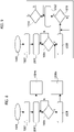
Figure 6 is a flow-chart exemplary of possible operation of embodiments of the present description, -
Figure 7 is a block diagram providing additional details with respect toFigures 4 and 5 , -
Figure 8 and Figure 9 are flow-charts exemplary of possible operation of embodiments of the present description, and -
Figure 10 is a block diagram representative of low-power mode operation of embodiments of the present description. - Corresponding numerals and symbols in the different figures generally refer to corresponding parts unless otherwise indicated. The figures are drawn to clearly illustrate the relevant aspects of the embodiments and are not necessarily drawn to scale. The edges of features drawn in the figures do not necessarily indicate the termination of the extent of the feature.
- In the ensuing description, various specific details are illustrated in order to provide an in-depth understanding of various examples of embodiments according to the description. The embodiments may be obtained without one or more of the specific details, or with other methods, components, materials, etc. In other cases, known structures, materials, or operations are not illustrated or described in detail so that various aspects of the embodiments will not be obscured.
- Reference to "an embodiment" or "one embodiment" in the framework of the present description is intended to indicate that a particular configuration, structure, or characteristic described in relation to the embodiment is comprised in at least one embodiment. Hence, phrases such as "in an embodiment", "in one embodiment", or the like, that may be present in various points of the present description do not necessarily refer exactly to one and the same embodiment. Furthermore, particular configurations, structures, or characteristics may be combined in any adequate way in one or more embodiments.
- The headings/references used herein are provided merely for convenience and hence do not define the extent of protection or the scope of the embodiments.
- For the sake of brevity and simplicity, a same designation (VBAT, VDDIO, and so on, for instance) may be used in the following to designate both a certain circuit node or line and a signal (a voltage signal, for instance) occurring at that node or line.
-
Figure 1 is a simplified representation of acircuit 10 such as, for instance, a MicroController Unit or MCU supplied via a supply source such as a battery LB, for instance. - A (rechargeable) lithium-ion battery may be exemplary of the battery LB. Those of skill in the art will otherwise appreciate that the embodiments are not limited to the presence of such a battery, which is otherwise distinct from the embodiments. For instance, the battery LB may be a battery intended to be coupled to the circuit 10 ("plugged-in") only by an end-user and/or over limited periods of time.
- A battery such as LB is representative of a supply source configured to apply to the circuit 10 a supply voltage between a "hot" node VDD and ground GND.
- As discussed in the foregoing, while batteries such as modern re-chargeable lithium-ion batteries have an operating voltage up to 4.5V and a (slightly) higher charging voltage, most commercial technologies do not include devices able/required to operate above 3.6V.
- Reaching higher voltages involves using "high-voltage" circuits that may be fairly complex and increase semiconductor area occupancy, cost and power consumption.
-
Figure 2 is exemplary of one such conventional approach where an (external)voltage regulator 12 is provided between the battery LB and the node VDD in thecircuit 10, with acoupling capacitor 14 provided between the node VDD and ground GND. - An arrangement as exemplified in
Figure 2 suffers from the presence of extra components, which negatively affect the Bill of Material, BoM, with increased size, complexity and cost. - Additional drawbacks involve increased power consumption in the active mode and also in a low-power (quiescent) mode.
- All of the foregoing renders the solution exemplified in
Figure 2 hardly attractive for applications such as IoT (Internet of Things) applications where reduced consumption in a low-power mode is desirable. - Another conventional approach as exemplified in
Figure 3 is based on System on Chip (SoC) architecture wherein theregulator 12 is "embedded" in thecircuit 10 with the provision of input/output (I/O)analog circuitry 16 similarly embedded in thecircuit 10. Thedecoupling capacitor 14 can be arranged between a node intermediate the embeddedregulator 12 and thecircuitry 16 and ground GND. - While providing slightly better performance, an arrangement as exemplified in
Figure 3 essentially suffers from the same drawbacks discussed in connection withFigure 2 . - One or more embodiments as exemplified herein, expand upon the embedded layout of the
Figure 3 by providing an embedded voltage regulator designated 100 as a whole. - For that reason, unless the context indicates otherwise, the general disclosure provided in the foregoing in connection with
Figures 1 to 3 also applies to the other figures and will not be repeated for brevity in connection with the figures fromFigure 4 onwards. - The
regulator 100 embedded in the circuit 10may be a low drop-out (LDO) regulator comprising high-drive LDO circuitry, designated 102, as well as low-power LDO circuitry, designated 104. - LDO is an acronym for "Low DropOut" and designates a DC linear voltage regulator architecture configured to regulate its output voltage (even) when the voltage supplied thereto is very close to the output voltage.
- As exemplified in
Figure 4 , theregulator 100 is configured to operate between: - a first node VBAT configured to have applied thereto the voltage from the supply source (e.g., 4.5V from a battery such LB), and
- a second node VDDIO configured to supply via a
line 180 an external device designated ED. - The device ED being designated "external" emphasizes that this may represent a distinct element from the
circuit 10. A memory such as flash memory coupled to an MCU such as 10 may be exemplary of such an external device ED. - As illustrated in
Figure 4 adecoupling capacitor 14 can be arranged intermediate the node VDDIO (line 180) and ground. - The
LDO regulator 100 thus receives at the node VBAT a voltage of 2.5V - 4.5V, for instance. This is the voltage that can be supplied from a battery such as LB coupled between the node VBAT and ground GND. - The (regulated) supply voltage applied to the external device ED by the node VDDIO (via the line 180) will expectedly be lower, in the 1.8V - 3.3V range.
- In
Figure 4 ,reference 16 again designates input/output (I/O) circuitry of an analog type, for instance, which can be assumed to be of the "always on" type, thus being capable of sensing the voltage at the node VDDIO. - Also, for the sake of this description one may assume that the
circuit 10 is configured to co-operate with the external device ED via a set of I/O nodes (pins) 18. - It will be otherwise appreciated that the specific characteristics and mode of operation of the I/
O circuitry 16 and the external device ED coupled with thecircuit 10 are of no specific relevance for the embodiments. - The embodiments can thus be regarded as essentially "transparent" the specific characteristics and mode operation of the
circuitry 16 and/or the external device ED. -
Reference 20 inFigure 4 denotes low-voltage digital logic circuitry intended to be supplied from the node VBAT at the input of theregulator 100 via a DC-DC (low-power mode)converter 22 configured to provide to the low-voltage digital logic 20a a supply voltage VDIG (1.1V, or 0.9V in low-power mode, for instance). - As illustrated herein, the embedded
regulator 100 is a dual-mode (high-drive and low-power) designed to have: - high consumption (only) when the circuit 10 (here, an MCU) into which the
regulator 100 is embedded is in a normal mode of operation, and - reduced consumption when the
circuit 10 is in low-power mode. - To that effect, the
regulator 100 can be designed (in a manner known per se to those of skill in the art) to include: - a high drive section or
circuitry 102 designed to provide adequate performance for dynamic activity (drive, and so on) even if this may involve a high quiescent current and/or low efficiency, and - a low-power section or
circuitry 102 designed to have performance limited, for instance, to wake-up capability and retention of the "live" state of thecircuit 10 when desired, with the advantage of reduced consumption compatible with low-power modes of theMCU 10. - It is noted that (as exemplified at 180) the embedded
regulator 100 can also be used to supply external devices ED, such as a memory, for instance. For instance, the external device ED can be a flash memory having operating voltages in the range of 1.8V to 3V (NOR) . -
Figure 5 further details the possibility for the embeddedregulator 100 to be incorporated together with the DC-DC low-power mode converter 22 to a power management unit within thecircuit 10. -
Figure 5 also details the possibility for thelogic circuitry 20 to include a processing unit orCPU 21 as well as a random-access memory (RAM), a read-only memory (ROM) and a one-time programmable (OTP)memory units - Briefly, an arrangement as illustrated herein is exemplary of a
circuit 10 comprising a first node, VBAT configured to receive a first voltage applied thereto as well as a second node, VDDIO configured to be coupled (see the line 180) with an electrically powered device ED such as a flash memory to provide electrical supply power to that device, with thecircuit 10 configured (e.g., via the pins 18) for communication with the device ED. - As illustrated, the
voltage regulator 100 embedded in thecircuit 10 is coupled to the first node VBAT and to the second node VDDIO to provide a regulated voltage at the second node towards the external device ED. - As illustrated, the
voltage regulator 100 includesfirst regulator circuitry 102 andsecond regulator circuitry 104 configured to provide full-power and low-power operation of thevoltage regulator 100. - An arrangement as detailed in
Figure 5 facilitates operating in such a way that at power-on theregulator 100 starts supplying the external device with a voltage that is reduced (e.g., below a supply threshold of 1.8V, for instance) to avoid potential damage to the external device (memory) ED. - The possibility will then exist to re-program the voltage provided by the embedded
LDO regulator 10 to higher voltages (3.3V, to support other devices, for instance) that is, with a regulated voltage from theLDO regulator 100 applied to the node VDDIO that may vary from 1.8V to 3.3V. - The
voltage regulator 100 is thus adapted to be activated in a first startup mode during which thevoltage regulator 100 applies to the second node VDDIO a voltage increasing towards a supply threshold. - The
circuit 10 comprises control circuitry such as 20 adapted to be activated (as detailed in the following) in response to the voltage at the output node VDDIO reaching the supply threshold. - The
control circuitry 20 is configured to bring thevoltage regulator 100 to a second mode of operation where thevoltage regulator 100 applies to the second node VDDIO a regulated voltage higher than the supply threshold. - The
control circuitry 20 comprises processing circuitry configured to (re)program the value of the regulated voltage at the node VDDIO to a value higher than the supply threshold discussed previously. - For instance,
voltage regulator 100 can be configured to receive at the node VBAT a voltage in a first voltage range between a lower bound (e.g., approximately 2.5V) and an upper bound (e.g., approximately 4.5V) and to apply to the second node, VDDIO a regulated voltage in a second voltage range between the supply threshold (e.g., approximately 1.8V) and a respective upper bound (e.g., approximately 3.3V). - It will be appreciated that, in the example considered herein, the lower bound of 2.5V is higher than the supply threshold of 1.8V and the upper bound of 4.5V is higher than the respective upper bound of 3.3V.
- Of course, the quantitative figures reported throughout the present description are merely exemplary and not limiting of the embodiments.
- A desired user configuration can thus be "pushed" via the
CPU 21 for instance through a firmware stored in the RAM memory or boot ROM/OTP from theblocks 23A to 23C. - In the flow-chart of
Figure 6 ,block 1000 is exemplary of start-up at power-on (due to a battery LB being coupled to the circuit 10). - After reset as represented by
block 1002, the high-drive circuitry in theLDO regulator 1000 is switched-on with the DC-DC converter 22 kept in an "off" (inactive) state, as represented byblock 1004 inFigure 6 . -
Block 1006 inFigure 6 is exemplary of a check as to whether the voltage at the node VDDIO has increased up to a certain threshold (1.8V, for instance). - A negative outcome (N) from the check of
step 1006 causes the circuitry to loop back. - Conversely, a positive outcome (Y) of the check 1006 (the voltage VDDIO has reached the threshold) causes switch-on of the DC-
DC converter 22 with the high-drive circuitry 102 in theLDO regulator 100 kept active as represented byblock 1008 in the flow-chart ofFigure 6 . - The diagram of
Figure 6A is exemplary of operation as discussed previously, showing the voltage VDDIO ramping up at a moderate rate with respect to VBAT towards the threshold designated TPOR (1.8V, for instance) to settle then at voltage of 1.8V plus an extra value Δ. - It is noted that, in operation as discussed previously, full operation is started only after the voltage at node VDDIO has reached an adequate level.
- This may involve an autonomous start-up of the LDO regulator 100 (high drive circuitry 102) as soon as the
circuit 10 is energized (battery LB plugged in, for instance). - As exemplified in
Figure 7 (as noted, corresponding parts or elements are indicated with corresponding reference symbols throughout the figures) a dedicated power-on reset (POR) voltage monitor 160 can be provided in thecircuitry 16, the voltage monitor 160 being sensitive to the voltage at the node VDDIO and may assert an enable signal vdig_en towards thepower management unit 105 to switch-on the DC-DC converter 22 and the digital logic 20 (including the CPU 21). - The flow-chart of
Figure 8 is an expanded version of the flow-chart ofFigure 6 showing that, at switch-on as represented byblock 1004, the LDO regulator may start at the lowest (minimum) voltage compatible with the external device ED, e.g., 1.8V. This is represented byblock 1004A inFigure 8 . - Also, block 1008A in the flow-chart of
Figure 8 is exemplary of the fact that once an (adequate) value VDIG is available for the DC-DC converter 22, a user can take control of the circuit operation (via theCPU 21, for instance) and re-program the LDO configuration registers to increase the LDO output voltage up to values compatible with proper external device operation (e.g., 3.3V) . - The flow-chart of
Figure 9 is a further expanded version of the flow-chart ofFigure 6 (andFigure 8 as well), showing the possibility for thecircuit 10 to evolve from the condition exemplified by block 1008 (DC-DC converter 22 switched-on with the LDO regulator having the high-drive circuitry 102 activated and the low-power circuitry 104 de-activated) to astep 1010 where a check is made as to whether a (software generated) request for low-power mode operation has been received. - Such a request may be generated (in a manner known per se to those of skill in the art) in response to conditions where activity of the circuit 10 (and the external device ED) has been limited over a time interval so that circuit performance can be limited, for instance, to wake-up capability and retention of the "live" state of the
circuit 10. - The external device ED can be similarly switched to a low-power mode. For instance, if the external device ED is a memory, such a memory may be unavailable for access during that time.
- In the case of a negative outcome (N) of the check at
bloc 1010, the system simply loops back. - In the presence of a positive outcome (Y) of the check of block 1010 (that is, a valid request for low-power operation has been received) the
circuit 10 is switched to a low-power, low-consumption state (as represented byblock 1012 inFigure 9 ) where theLDO regulator 10 is switched to low-power operation with the high-drive circuitry 102 de-activated (turned-off), the low-power circuitry 104 activated (turned-on), and the DC-DC converter 22 de-activated. - At this point, the circuit evolves to a state (exemplified by block 1014) where a check is made as to the occurrence of any "wake-up" event.
- Such an event may correspond to dynamic activity of the circuit 10 (and the external device ED) being resumed with adequate performance involved.
- In the case of a negative outcome (N) of the check of block 1o14, the circuit simply loops back.
- Conversely, in the presence of a positive outcome (Y) of the check of block 1014 (a wake-up event has occurred) operation is returned to the
block 1008, wherein theLDO regulator 100 with the high-drive circuitry 102 activated (turned-on) and the low-power circuitry 104 de-activated (turned-off) with the DC-DC converter 22 likewise (re)activated. - In the low-power mode, as exemplified by
block 1012 inFigure 10 , theLDO regulator 100 is still active, but in a low-power mode, in contrast with the high-drive mode as exemplified byblock 1008 inFigure 10 . - The
LDO regulator 100 can be switched to the low-power mode in response to the DC-DC converter 22 being requested to be switched-off via the signal vdig_en being set, for instance to "0", due to a low-power mode request (indicated by a block designated 1010 for consistency with the homologous block in the flow-chart ofFigure 9 ) sent tologic circuitry 162 in thecircuitry 16 that is also sensitive to wake-up events WU. - The
LDO regulator 100 can be switched (back) to a high-power mode (high-drive circuitry 102 turned-on and low-power circuitry 104 turned-off, respectively) in response to wake-up being requested (e.g., via vdig_en being set to "1"). - The logic value for vdig_en may thus result from a combination of a signal from the power-on
reset circuit 160, a low-power mode request 1010 from theCPU 21, for instance, and a wake-up request WU as possibly received from the outer environment or an internal timer. - As illustrated in
Figure 10 , a low-power mode request such as 1010 can be triggered (via software) by theCPU 21 as currently occurring in microcontrollers. - Wake-up requests WU may be received via external pins (or, possibly, from internal sources such as real-time clock RTC).
- One or more embodiments may thus provide extended operating voltage ranges up to, e.g., 4.5V, with reduced semiconductor area occupancy and reduced power consumption, cost, while also providing support for low-power modes compatible with applications such as Internet of Things (IoT) applications, for instance.
- One or more embodiments facilitate providing devices supporting high-voltage supply as desirable for lithium-ion batteries having an operating voltage in the range of 4.5V, for instance.
- One or more embodiments also facilitate supplying an external device (such as a flash memory, for instance) in a safe way, without risk of damage at power-on.
- Without prejudice to the underlying principles, the details and embodiments may vary, even significantly, with respect to what has been described in the foregoing, by way of example only, without departing from the extent of protection.
- The extent of protection is determined by the annexed claims.
Claims (14)
- A circuit (10), comprising:a first node (VBAT) configured to receive a first voltage applied thereto,a second node (VDDIO) configured to be coupled (180) with an electrically powered device (ED) to provide electrical supply power to said electrically powered device (ED), wherein the circuit (10) is configured (18) for communication with said electrically powered device (ED),a voltage regulator (100) coupled to the first node (VBAT) and the second node (VDDIO) to provide a regulated voltage at the second node (VDDIO),wherein:the voltage regulator (100) is activatable in a first, startup mode (1000, 1002) during which the voltage regulator (100) applies to said second node (VDDIO) a voltage increasing towards a supply threshold (TPOR), andthe circuit (10) comprises control circuitry (20) activatable (16, 160, vdig_en, 22) in response (1006, Y) to the voltage at said second node (VDDIO) reaching said supply threshold (160, TPOR), the control circuitry (20) configured, when activated, to bring (21, 24, LDOIO config) the voltage regulator (100) to a second mode of operation (1008) of the voltage regulator (100) wherein the voltage regulator (100) applies to said second node (VDDIO) a regulated voltage higher than said supply threshold (TPOR).
- The circuit (10) of claim 1, wherein the control circuitry (20) comprises processing circuitry (21) configured (23A, 23B, 23C) to program (LDOIO config) the value of said regulated voltage higher than said supply threshold (TPOR).
- The circuit (10) of claim 1 or claim 2, wherein the voltage regulator (100) is configured to:receive at said first node (VBAT) a voltage in a first voltage range between a lower bound and an upper bound, andapply to said second node (VDDIO), in said second mode of operation (1008) of the voltage regulator (100), a regulated voltage in a second voltage range between said supply threshold (TPOR) and a respective upper bound,wherein said lower bound is higher than said supply threshold (TPOR) and said upper bound is higher than said respective upper bound.
- The circuit (10) of claim 3, wherein said lower bound and said upper bound are, approximately, 2.5V and 4.5V.
- The circuit (10) of claim 3 or claim 4, wherein said supply threshold (TPOR) and said respective upper bound are, approximately, 1.8V and 3.3V.
- The circuit (10) of any of the previous claims, comprising a supply circuit (22) of the control circuitry (20), the supply circuit (22) coupled (160, vdig_en) to said second node (VDDIO) and activatable in response (1006, Y) to the voltage at said second node (VDDIO) reaching said supply threshold (160, TPOR).
- The circuit (10) of any of the previous claims, wherein:the voltage regulator (100) includes first regulator circuitry (102) and second regulator circuitry (104) configured to provide full-power and low-power operation of the voltage regulator (100), andthe circuit (100) is configured (162) to receive low-power operation request signals (1010) and, in response to low-power operation request signals (1010) received, to deactivate the first regulator circuitry (102) in the voltage regulator (100) and activate the second regulator circuitry (104) in the voltage regulator (100) in a third, low-power mode of operation (1012) of the voltage regulator (100).
- The circuit (10) of claim 6 and claim 7, wherein the control circuitry (16, 20, 22) is configured to deactivate (vidg_en) said supply circuit (22) in said third, low-power mode of operation (1012) of the voltage regulator (100).
- The circuit (10) of claim 7 or claim 8, wherein the circuit is configured (162) to receive wake-up signals (WU) and, in response to wake-up signals (WU) received (1014), bring the voltage regulator (100) from said third, low-power mode of operation mode (1012) back to said second mode of operation (1008) of the voltage regulator (100).
- The circuit (10) of any of the previous claims, wherein the voltage regulator (100) is activatable in said first, startup mode (1000, 1002) in response to a supply source (LB) being coupled to the first node (VBAT).
- The circuit (10) of any of the previous claims, wherein:the voltage regulator (100) comprises a Low DropOut, LDO regulator, and/orthe circuit (10) comprises a microcontroller unit.
- A system comprising:a circuit (10) according to any of the previous claims, andan electrically powered device (ED) coupled to said second node (VDDIO).
- The system of claim 12, wherein the electrically powered device (ED) coupled to said second node (VDDIO) comprises a memory.
- A method of operating a circuit (10) according to any of claims 1 to 11, the method comprising:coupling an electrically powered device (ED) to said second node (VDDIO), andcoupling a supply source (LB) to said first node (VBAT), wherein the voltage regulator (100) is activated in said first startup mode (1000, 1002) in response to said supply source (LB) being coupled to said first node (VBAT).
Applications Claiming Priority (1)
| Application Number | Priority Date | Filing Date | Title |
|---|---|---|---|
| IT102021000015197A IT202100015197A1 (en) | 2021-06-10 | 2021-06-10 | Corresponding power circuit, device and method |
Publications (2)
| Publication Number | Publication Date |
|---|---|
| EP4102335A1 true EP4102335A1 (en) | 2022-12-14 |
| EP4102335B1 EP4102335B1 (en) | 2026-03-25 |
Family
ID=77519683
Family Applications (1)
| Application Number | Title | Priority Date | Filing Date |
|---|---|---|---|
| EP22305741.5A Active EP4102335B1 (en) | 2021-06-10 | 2022-05-19 | Power supply circuit, corresponding device and method |
Country Status (3)
| Country | Link |
|---|---|
| US (1) | US11906994B2 (en) |
| EP (1) | EP4102335B1 (en) |
| IT (1) | IT202100015197A1 (en) |
Citations (4)
| Publication number | Priority date | Publication date | Assignee | Title |
|---|---|---|---|---|
| US20170054356A1 (en) * | 2007-03-12 | 2017-02-23 | Tamiras Per Pte. Ltd., Llc | Intelligent voltage regulator |
| WO2018060990A1 (en) * | 2016-09-28 | 2018-04-05 | B. G. Negev Technologies And Applications Ltd., At Ben-Gurion University | Digital average current-mode control voltage regulator and a method for tuning compensation coefficients thereof |
| US20200326739A1 (en) * | 2017-12-29 | 2020-10-15 | Beijing Smartchip Microelectronics Technology Company Limited | Ultra-low power consumption power supply structure |
| US11029716B1 (en) * | 2020-02-18 | 2021-06-08 | Silicon Laboratories Inc. | Providing low power charge pump for integrated circuit |
Family Cites Families (10)
| Publication number | Priority date | Publication date | Assignee | Title |
|---|---|---|---|---|
| US7459891B2 (en) * | 2006-03-15 | 2008-12-02 | Texas Instruments Incorporated | Soft-start circuit and method for low-dropout voltage regulators |
| US7619397B2 (en) * | 2006-11-14 | 2009-11-17 | Texas Instruments Incorporated | Soft-start circuit for power regulators |
| US7782038B2 (en) * | 2007-03-23 | 2010-08-24 | Fairchild Semiconductor Corporation | Soft start circuit with slew rate controller for voltage regulators |
| WO2010020837A1 (en) | 2008-08-22 | 2010-02-25 | Freescale Semiconductor, Inc. | Voltage regulator with low and high power modes |
| US8145934B1 (en) * | 2009-07-31 | 2012-03-27 | Western Digital Technologies, Inc. | Soft start sequencer for starting multiple voltage regulators |
| US8552703B2 (en) | 2011-03-04 | 2013-10-08 | Intersil Americas Inc. | Method and apparatus for low standby current switching regulator |
| US9360928B2 (en) | 2012-07-27 | 2016-06-07 | Atmel Corporation | Dual regulator systems |
| US10895884B2 (en) * | 2017-11-14 | 2021-01-19 | Semiconductor Components Industries, Llc | Low dropout (LDO) voltage regulator with soft-start circuit |
| TWI652888B (en) * | 2017-11-24 | 2019-03-01 | 緯創資通股份有限公司 | Single input multi-output DC power supply system and related buck regulation control circuit |
| US10872640B2 (en) | 2018-08-31 | 2020-12-22 | Micron Technology, Inc. | Capacitive voltage dividers coupled to voltage regulators |
-
2021
- 2021-06-10 IT IT102021000015197A patent/IT202100015197A1/en unknown
-
2022
- 2022-05-19 EP EP22305741.5A patent/EP4102335B1/en active Active
- 2022-06-09 US US17/836,524 patent/US11906994B2/en active Active
Patent Citations (4)
| Publication number | Priority date | Publication date | Assignee | Title |
|---|---|---|---|---|
| US20170054356A1 (en) * | 2007-03-12 | 2017-02-23 | Tamiras Per Pte. Ltd., Llc | Intelligent voltage regulator |
| WO2018060990A1 (en) * | 2016-09-28 | 2018-04-05 | B. G. Negev Technologies And Applications Ltd., At Ben-Gurion University | Digital average current-mode control voltage regulator and a method for tuning compensation coefficients thereof |
| US20200326739A1 (en) * | 2017-12-29 | 2020-10-15 | Beijing Smartchip Microelectronics Technology Company Limited | Ultra-low power consumption power supply structure |
| US11029716B1 (en) * | 2020-02-18 | 2021-06-08 | Silicon Laboratories Inc. | Providing low power charge pump for integrated circuit |
Also Published As
| Publication number | Publication date |
|---|---|
| US11906994B2 (en) | 2024-02-20 |
| EP4102335B1 (en) | 2026-03-25 |
| IT202100015197A1 (en) | 2022-12-10 |
| US20220397923A1 (en) | 2022-12-15 |
Similar Documents
| Publication | Publication Date | Title |
|---|---|---|
| CN112083791B (en) | Chip power consumption optimization method, apparatus, computer equipment and storage medium | |
| CN205753551U (en) | Battery and battery core control circuit thereof and aircraft | |
| US20210311540A1 (en) | Power-saving power architecture for integrated circuits such as microcontrollers | |
| CN111711436A (en) | A power-off and reset circuit and intelligent central control | |
| CN204009457U (en) | On/off circuit based on PMU and electronic equipment | |
| US11372470B2 (en) | Control system for controlling intelligent system to reduce power consumption based on bluetooth device | |
| CN104054247A (en) | Integrated circuit device with integrated voltage controller | |
| CN109799898A (en) | Chip power supply control device, chip and power supply control method thereof | |
| TW201348945A (en) | Power source controlling system and method | |
| WO2021078261A1 (en) | Power supply control method, system and device | |
| CN114974329B (en) | Shutdown control device for autonomous vehicles and autonomous vehicles | |
| CN113708467B (en) | Electrifying circuit, battery backup unit and storage server system | |
| US11906994B2 (en) | Power supply circuit, corresponding device and method | |
| CN107561991A (en) | A kind of switching on and shutting down management circuit and terminal | |
| US20100244911A1 (en) | Supply circuitry for sleep mode | |
| US20240403062A1 (en) | Boot cluster indication in a computer system | |
| CN116954345A (en) | Wake-up circuit and electronic equipment | |
| CN212659300U (en) | Low-voltage starting circuit for buzzer | |
| CN209642544U (en) | A kind of low-loss multivoltage boot-strap circuit with delay protection function | |
| US8659442B2 (en) | Power-saving reminder circuit for computer | |
| CN113467333B (en) | Startup control circuit and startup control method | |
| CN111465911B (en) | Low inrush current circuit for power-up and deep power-down exit | |
| CN115473297A (en) | Power supply circuit, corresponding device and method | |
| CN112117819A (en) | Battery-less power supply method and circuit design | |
| CN105204403A (en) | Clock circuit, power supply control method based on clock circuit and air conditioner |
Legal Events
| Date | Code | Title | Description |
|---|---|---|---|
| PUAI | Public reference made under article 153(3) epc to a published international application that has entered the european phase |
Free format text: ORIGINAL CODE: 0009012 |
|
| STAA | Information on the status of an ep patent application or granted ep patent |
Free format text: STATUS: REQUEST FOR EXAMINATION WAS MADE |
|
| 17P | Request for examination filed |
Effective date: 20220519 |
|
| AK | Designated contracting states |
Kind code of ref document: A1 Designated state(s): AL AT BE BG CH CY CZ DE DK EE ES FI FR GB GR HR HU IE IS IT LI LT LU LV MC MK MT NL NO PL PT RO RS SE SI SK SM TR |
|
| GRAP | Despatch of communication of intention to grant a patent |
Free format text: ORIGINAL CODE: EPIDOSNIGR1 |
|
| STAA | Information on the status of an ep patent application or granted ep patent |
Free format text: STATUS: GRANT OF PATENT IS INTENDED |
|
| INTG | Intention to grant announced |
Effective date: 20251120 |
|
| GRAS | Grant fee paid |
Free format text: ORIGINAL CODE: EPIDOSNIGR3 |
|
| GRAA | (expected) grant |
Free format text: ORIGINAL CODE: 0009210 |
|
| STAA | Information on the status of an ep patent application or granted ep patent |
Free format text: STATUS: THE PATENT HAS BEEN GRANTED |
|
| AK | Designated contracting states |
Kind code of ref document: B1 Designated state(s): AL AT BE BG CH CY CZ DE DK EE ES FI FR GB GR HR HU IE IS IT LI LT LU LV MC MK MT NL NO PL PT RO RS SE SI SK SM TR |
|
| REG | Reference to a national code |
Ref country code: CH Ref legal event code: F10 Free format text: ST27 STATUS EVENT CODE: U-0-0-F10-F00 (AS PROVIDED BY THE NATIONAL OFFICE) Effective date: 20260325 Ref country code: GB Ref legal event code: FG4D |
|
| REG | Reference to a national code |
Ref country code: DE Ref legal event code: R096 Ref document number: 602022032922 Country of ref document: DE |
|
| REG | Reference to a national code |
Ref country code: IE Ref legal event code: FG4D |
|
| PG25 | Lapsed in a contracting state [announced via postgrant information from national office to epo] |
Ref country code: RS Free format text: LAPSE BECAUSE OF FAILURE TO SUBMIT A TRANSLATION OF THE DESCRIPTION OR TO PAY THE FEE WITHIN THE PRESCRIBED TIME-LIMIT Effective date: 20260625 |
|
| PG25 | Lapsed in a contracting state [announced via postgrant information from national office to epo] |
Ref country code: GR Free format text: LAPSE BECAUSE OF FAILURE TO SUBMIT A TRANSLATION OF THE DESCRIPTION OR TO PAY THE FEE WITHIN THE PRESCRIBED TIME-LIMIT Effective date: 20260626 |
|
| REG | Reference to a national code |
Ref country code: LT Ref legal event code: MG9D |
|
| PG25 | Lapsed in a contracting state [announced via postgrant information from national office to epo] |
Ref country code: LT Free format text: LAPSE BECAUSE OF FAILURE TO SUBMIT A TRANSLATION OF THE DESCRIPTION OR TO PAY THE FEE WITHIN THE PRESCRIBED TIME-LIMIT Effective date: 20260325 |
|
| PGFP | Annual fee paid to national office [announced via postgrant information from national office to epo] |
Ref country code: DE Payment date: 20260421 Year of fee payment: 5 |
|
| PG25 | Lapsed in a contracting state [announced via postgrant information from national office to epo] |
Ref country code: NO Free format text: LAPSE BECAUSE OF FAILURE TO SUBMIT A TRANSLATION OF THE DESCRIPTION OR TO PAY THE FEE WITHIN THE PRESCRIBED TIME-LIMIT Effective date: 20260625 |
|
| PG25 | Lapsed in a contracting state [announced via postgrant information from national office to epo] |
Ref country code: SE Free format text: LAPSE BECAUSE OF FAILURE TO SUBMIT A TRANSLATION OF THE DESCRIPTION OR TO PAY THE FEE WITHIN THE PRESCRIBED TIME-LIMIT Effective date: 20260325 Ref country code: FI Free format text: LAPSE BECAUSE OF FAILURE TO SUBMIT A TRANSLATION OF THE DESCRIPTION OR TO PAY THE FEE WITHIN THE PRESCRIBED TIME-LIMIT Effective date: 20260325 |
|
| PG25 | Lapsed in a contracting state [announced via postgrant information from national office to epo] |
Ref country code: HR Free format text: LAPSE BECAUSE OF FAILURE TO SUBMIT A TRANSLATION OF THE DESCRIPTION OR TO PAY THE FEE WITHIN THE PRESCRIBED TIME-LIMIT Effective date: 20260325 |
|
| PG25 | Lapsed in a contracting state [announced via postgrant information from national office to epo] |
Ref country code: LV Free format text: LAPSE BECAUSE OF FAILURE TO SUBMIT A TRANSLATION OF THE DESCRIPTION OR TO PAY THE FEE WITHIN THE PRESCRIBED TIME-LIMIT Effective date: 20260325 |
|
| PG25 | Lapsed in a contracting state [announced via postgrant information from national office to epo] |
Ref country code: BG Free format text: LAPSE BECAUSE OF FAILURE TO SUBMIT A TRANSLATION OF THE DESCRIPTION OR TO PAY THE FEE WITHIN THE PRESCRIBED TIME-LIMIT Effective date: 20260325 |
|
| REG | Reference to a national code |
Ref country code: NL Ref legal event code: MP Effective date: 20260325 |