EP4099550A1 - Transformer-less ac-dc input compatible boost resonant inverter - Google Patents
Transformer-less ac-dc input compatible boost resonant inverter Download PDFInfo
- Publication number
- EP4099550A1 EP4099550A1 EP22171661.6A EP22171661A EP4099550A1 EP 4099550 A1 EP4099550 A1 EP 4099550A1 EP 22171661 A EP22171661 A EP 22171661A EP 4099550 A1 EP4099550 A1 EP 4099550A1
- Authority
- EP
- European Patent Office
- Prior art keywords
- line
- stage
- coupled
- rail
- parallel
- Prior art date
- Legal status (The legal status is an assumption and is not a legal conclusion. Google has not performed a legal analysis and makes no representation as to the accuracy of the status listed.)
- Pending
Links
Images

Classifications
-
- H—ELECTRICITY
- H02—GENERATION; CONVERSION OR DISTRIBUTION OF ELECTRIC POWER
- H02M—APPARATUS FOR CONVERSION BETWEEN AC AND AC, BETWEEN AC AND DC, OR BETWEEN DC AND DC, AND FOR USE WITH MAINS OR SIMILAR POWER SUPPLY SYSTEMS; CONVERSION OF DC OR AC INPUT POWER INTO SURGE OUTPUT POWER; CONTROL OR REGULATION THEREOF
- H02M1/00—Details of apparatus for conversion
- H02M1/42—Circuits or arrangements for compensating for or adjusting power factor in converters or inverters
- H02M1/4208—Arrangements for improving power factor of AC input
- H02M1/4233—Arrangements for improving power factor of AC input using a bridge converter comprising active switches
-
- A—HUMAN NECESSITIES
- A61—MEDICAL OR VETERINARY SCIENCE; HYGIENE
- A61L—METHODS OR APPARATUS FOR STERILISING MATERIALS OR OBJECTS IN GENERAL; DISINFECTION, STERILISATION OR DEODORISATION OF AIR; CHEMICAL ASPECTS OF BANDAGES, DRESSINGS, ABSORBENT PADS OR SURGICAL ARTICLES; MATERIALS FOR BANDAGES, DRESSINGS, ABSORBENT PADS OR SURGICAL ARTICLES
- A61L2/00—Disinfection or sterilisation of materials or objects, in general; Accessories therefor
- A61L2/02—Disinfection or sterilisation of materials or objects, in general; Accessories therefor using physical processes
- A61L2/08—Radiation
- A61L2/10—Ultraviolet [UV] radiation
-
- A—HUMAN NECESSITIES
- A61—MEDICAL OR VETERINARY SCIENCE; HYGIENE
- A61L—METHODS OR APPARATUS FOR STERILISING MATERIALS OR OBJECTS IN GENERAL; DISINFECTION, STERILISATION OR DEODORISATION OF AIR; CHEMICAL ASPECTS OF BANDAGES, DRESSINGS, ABSORBENT PADS OR SURGICAL ARTICLES; MATERIALS FOR BANDAGES, DRESSINGS, ABSORBENT PADS OR SURGICAL ARTICLES
- A61L2/00—Disinfection or sterilisation of materials or objects, in general; Accessories therefor
- A61L2/26—Accessories
-
- B—PERFORMING OPERATIONS; TRANSPORTING
- B64—AIRCRAFT; AVIATION; COSMONAUTICS
- B64D—EQUIPMENT FOR FITTING IN OR TO AIRCRAFT; FLIGHT SUITS; PARACHUTES; ARRANGEMENT OR MOUNTING OF POWER PLANTS OR PROPULSION TRANSMISSIONS IN AIRCRAFT
- B64D47/00—Equipment not otherwise provided for
- B64D47/02—Arrangements or adaptations of signal or lighting devices
-
- H—ELECTRICITY
- H02—GENERATION; CONVERSION OR DISTRIBUTION OF ELECTRIC POWER
- H02M—APPARATUS FOR CONVERSION BETWEEN AC AND AC, BETWEEN AC AND DC, OR BETWEEN DC AND DC, AND FOR USE WITH MAINS OR SIMILAR POWER SUPPLY SYSTEMS; CONVERSION OF DC OR AC INPUT POWER INTO SURGE OUTPUT POWER; CONTROL OR REGULATION THEREOF
- H02M1/00—Details of apparatus for conversion
- H02M1/10—Arrangements incorporating converting means for enabling loads to be operated at will from different kinds of power supplies, e.g. from AC or DC
-
- H—ELECTRICITY
- H02—GENERATION; CONVERSION OR DISTRIBUTION OF ELECTRIC POWER
- H02M—APPARATUS FOR CONVERSION BETWEEN AC AND AC, BETWEEN AC AND DC, OR BETWEEN DC AND DC, AND FOR USE WITH MAINS OR SIMILAR POWER SUPPLY SYSTEMS; CONVERSION OF DC OR AC INPUT POWER INTO SURGE OUTPUT POWER; CONTROL OR REGULATION THEREOF
- H02M1/00—Details of apparatus for conversion
- H02M1/42—Circuits or arrangements for compensating for or adjusting power factor in converters or inverters
- H02M1/4208—Arrangements for improving power factor of AC input
- H02M1/4225—Arrangements for improving power factor of AC input using a non-isolated boost converter
-
- H—ELECTRICITY
- H02—GENERATION; CONVERSION OR DISTRIBUTION OF ELECTRIC POWER
- H02M—APPARATUS FOR CONVERSION BETWEEN AC AND AC, BETWEEN AC AND DC, OR BETWEEN DC AND DC, AND FOR USE WITH MAINS OR SIMILAR POWER SUPPLY SYSTEMS; CONVERSION OF DC OR AC INPUT POWER INTO SURGE OUTPUT POWER; CONTROL OR REGULATION THEREOF
- H02M7/00—Conversion of AC power input into DC power output; Conversion of DC power input into AC power output
- H02M7/42—Conversion of DC power input into AC power output without possibility of reversal
- H02M7/44—Conversion of DC power input into AC power output without possibility of reversal by static converters
- H02M7/48—Conversion of DC power input into AC power output without possibility of reversal by static converters using discharge tubes with control electrode or semiconductor devices with control electrode
- H02M7/4815—Resonant converters
-
- H—ELECTRICITY
- H02—GENERATION; CONVERSION OR DISTRIBUTION OF ELECTRIC POWER
- H02M—APPARATUS FOR CONVERSION BETWEEN AC AND AC, BETWEEN AC AND DC, OR BETWEEN DC AND DC, AND FOR USE WITH MAINS OR SIMILAR POWER SUPPLY SYSTEMS; CONVERSION OF DC OR AC INPUT POWER INTO SURGE OUTPUT POWER; CONTROL OR REGULATION THEREOF
- H02M7/00—Conversion of AC power input into DC power output; Conversion of DC power input into AC power output
- H02M7/42—Conversion of DC power input into AC power output without possibility of reversal
- H02M7/44—Conversion of DC power input into AC power output without possibility of reversal by static converters
- H02M7/48—Conversion of DC power input into AC power output without possibility of reversal by static converters using discharge tubes with control electrode or semiconductor devices with control electrode
- H02M7/53—Conversion of DC power input into AC power output without possibility of reversal by static converters using discharge tubes with control electrode or semiconductor devices with control electrode using devices of a triode or transistor type requiring continuous application of a control signal
- H02M7/537—Conversion of DC power input into AC power output without possibility of reversal by static converters using discharge tubes with control electrode or semiconductor devices with control electrode using devices of a triode or transistor type requiring continuous application of a control signal using semiconductor devices only, e.g. single switched pulse inverters
- H02M7/5387—Conversion of DC power input into AC power output without possibility of reversal by static converters using discharge tubes with control electrode or semiconductor devices with control electrode using devices of a triode or transistor type requiring continuous application of a control signal using semiconductor devices only, e.g. single switched pulse inverters in a bridge configuration
-
- H—ELECTRICITY
- H05—ELECTRIC TECHNIQUES NOT OTHERWISE PROVIDED FOR
- H05B—ELECTRIC HEATING; ELECTRIC LIGHT SOURCES NOT OTHERWISE PROVIDED FOR; CIRCUIT ARRANGEMENTS FOR ELECTRIC LIGHT SOURCES, IN GENERAL
- H05B41/00—Circuit arrangements or apparatus for igniting or operating discharge lamps
- H05B41/14—Circuit arrangements
- H05B41/36—Controlling
-
- H—ELECTRICITY
- H05—ELECTRIC TECHNIQUES NOT OTHERWISE PROVIDED FOR
- H05B—ELECTRIC HEATING; ELECTRIC LIGHT SOURCES NOT OTHERWISE PROVIDED FOR; CIRCUIT ARRANGEMENTS FOR ELECTRIC LIGHT SOURCES, IN GENERAL
- H05B45/00—Circuit arrangements for operating light-emitting diodes [LED]
- H05B45/30—Driver circuits
- H05B45/355—Power factor correction [PFC]; Reactive power compensation
-
- H—ELECTRICITY
- H05—ELECTRIC TECHNIQUES NOT OTHERWISE PROVIDED FOR
- H05B—ELECTRIC HEATING; ELECTRIC LIGHT SOURCES NOT OTHERWISE PROVIDED FOR; CIRCUIT ARRANGEMENTS FOR ELECTRIC LIGHT SOURCES, IN GENERAL
- H05B45/00—Circuit arrangements for operating light-emitting diodes [LED]
- H05B45/30—Driver circuits
- H05B45/37—Converter circuits
- H05B45/3725—Switched mode power supply [SMPS]
- H05B45/39—Circuits containing inverter bridges
-
- A—HUMAN NECESSITIES
- A61—MEDICAL OR VETERINARY SCIENCE; HYGIENE
- A61L—METHODS OR APPARATUS FOR STERILISING MATERIALS OR OBJECTS IN GENERAL; DISINFECTION, STERILISATION OR DEODORISATION OF AIR; CHEMICAL ASPECTS OF BANDAGES, DRESSINGS, ABSORBENT PADS OR SURGICAL ARTICLES; MATERIALS FOR BANDAGES, DRESSINGS, ABSORBENT PADS OR SURGICAL ARTICLES
- A61L2103/00—Materials or objects being the target of disinfection or sterilisation
- A61L2103/75—Room floors or walls
-
- A—HUMAN NECESSITIES
- A61—MEDICAL OR VETERINARY SCIENCE; HYGIENE
- A61L—METHODS OR APPARATUS FOR STERILISING MATERIALS OR OBJECTS IN GENERAL; DISINFECTION, STERILISATION OR DEODORISATION OF AIR; CHEMICAL ASPECTS OF BANDAGES, DRESSINGS, ABSORBENT PADS OR SURGICAL ARTICLES; MATERIALS FOR BANDAGES, DRESSINGS, ABSORBENT PADS OR SURGICAL ARTICLES
- A61L2202/00—Aspects relating to methods or apparatus for disinfecting or sterilising materials or objects
- A61L2202/10—Apparatus features
- A61L2202/11—Apparatus for generating biocidal substances, e.g. vaporisers, UV lamps
-
- B—PERFORMING OPERATIONS; TRANSPORTING
- B64—AIRCRAFT; AVIATION; COSMONAUTICS
- B64D—EQUIPMENT FOR FITTING IN OR TO AIRCRAFT; FLIGHT SUITS; PARACHUTES; ARRANGEMENT OR MOUNTING OF POWER PLANTS OR PROPULSION TRANSMISSIONS IN AIRCRAFT
- B64D2203/00—Aircraft or airfield lights using LEDs
-
- H—ELECTRICITY
- H01—ELECTRIC ELEMENTS
- H01J—ELECTRIC DISCHARGE TUBES OR DISCHARGE LAMPS
- H01J61/00—Gas-discharge or vapour-discharge lamps
- H01J61/02—Details
- H01J61/12—Selection of substances for gas fillings; Specified operating pressure or temperature
-
- H—ELECTRICITY
- H02—GENERATION; CONVERSION OR DISTRIBUTION OF ELECTRIC POWER
- H02M—APPARATUS FOR CONVERSION BETWEEN AC AND AC, BETWEEN AC AND DC, OR BETWEEN DC AND DC, AND FOR USE WITH MAINS OR SIMILAR POWER SUPPLY SYSTEMS; CONVERSION OF DC OR AC INPUT POWER INTO SURGE OUTPUT POWER; CONTROL OR REGULATION THEREOF
- H02M5/00—Conversion of AC power input into AC power output, e.g. for change of voltage, for change of frequency, for change of number of phases
- H02M5/40—Conversion of AC power input into AC power output, e.g. for change of voltage, for change of frequency, for change of number of phases with intermediate conversion into DC
- H02M5/42—Conversion of AC power input into AC power output, e.g. for change of voltage, for change of frequency, for change of number of phases with intermediate conversion into DC by static converters
- H02M5/44—Conversion of AC power input into AC power output, e.g. for change of voltage, for change of frequency, for change of number of phases with intermediate conversion into DC by static converters using discharge tubes or semiconductor devices to convert the intermediate DC into AC
- H02M5/453—Conversion of AC power input into AC power output, e.g. for change of voltage, for change of frequency, for change of number of phases with intermediate conversion into DC by static converters using discharge tubes or semiconductor devices to convert the intermediate DC into AC using devices of a triode or transistor type requiring continuous application of a control signal
- H02M5/458—Conversion of AC power input into AC power output, e.g. for change of voltage, for change of frequency, for change of number of phases with intermediate conversion into DC by static converters using discharge tubes or semiconductor devices to convert the intermediate DC into AC using devices of a triode or transistor type requiring continuous application of a control signal using semiconductor devices only
- H02M5/4585—Conversion of AC power input into AC power output, e.g. for change of voltage, for change of frequency, for change of number of phases with intermediate conversion into DC by static converters using discharge tubes or semiconductor devices to convert the intermediate DC into AC using devices of a triode or transistor type requiring continuous application of a control signal using semiconductor devices only having a rectifier with controlled elements
-
- Y—GENERAL TAGGING OF NEW TECHNOLOGICAL DEVELOPMENTS; GENERAL TAGGING OF CROSS-SECTIONAL TECHNOLOGIES SPANNING OVER SEVERAL SECTIONS OF THE IPC; TECHNICAL SUBJECTS COVERED BY FORMER USPC CROSS-REFERENCE ART COLLECTIONS [XRACs] AND DIGESTS
- Y02—TECHNOLOGIES OR APPLICATIONS FOR MITIGATION OR ADAPTATION AGAINST CLIMATE CHANGE
- Y02B—CLIMATE CHANGE MITIGATION TECHNOLOGIES RELATED TO BUILDINGS, e.g. HOUSING, HOUSE APPLIANCES OR RELATED END-USER APPLICATIONS
- Y02B20/00—Energy efficient lighting technologies, e.g. halogen lamps or gas discharge lamps
-
- Y—GENERAL TAGGING OF NEW TECHNOLOGICAL DEVELOPMENTS; GENERAL TAGGING OF CROSS-SECTIONAL TECHNOLOGIES SPANNING OVER SEVERAL SECTIONS OF THE IPC; TECHNICAL SUBJECTS COVERED BY FORMER USPC CROSS-REFERENCE ART COLLECTIONS [XRACs] AND DIGESTS
- Y02—TECHNOLOGIES OR APPLICATIONS FOR MITIGATION OR ADAPTATION AGAINST CLIMATE CHANGE
- Y02B—CLIMATE CHANGE MITIGATION TECHNOLOGIES RELATED TO BUILDINGS, e.g. HOUSING, HOUSE APPLIANCES OR RELATED END-USER APPLICATIONS
- Y02B70/00—Technologies for an efficient end-user side electric power management and consumption
- Y02B70/10—Technologies improving the efficiency by using switched-mode power supplies [SMPS], i.e. efficient power electronics conversion e.g. power factor correction or reduction of losses in power supplies or efficient standby modes
Definitions
- the present disclosure relates to systems and methods for providing relatively high voltage, high frequency power to an excimer bulb for use in aviation that avoids use of transformers.
- UV light has been found to be an effective disinfectant. Of the various UV wavelengths, 222 nanometers (222 nm) has been found to be particularly promising (effective and relatively safe for humans in moderate doses).
- 222 nanometers 222 nm
- Conventional power supplies for these excimer bulbs utilize transformers (e.g., they may utilize a resonant inverter that includes transformers) which has significant limitations. These limitations may include the following: the transformer may be relatively high voltage, resulting in relatively great power losses.
- the power stage of the power supply may have a degrading efficiency due to changes in electrical parameters of the excimer bulb over its life.
- the excimer bulb may lack ignition in certain situations due to voltage variations with fixed low direct current (DC) voltages.
- DC direct current
- the system includes a first stage circuit having: a first input line coupled to a first stage first parallel line having a first stage first switch positioned thereon, a second input line coupled to a first stage second parallel line having a first stage second switch positioned thereon, and a first stage third parallel line oriented in parallel with the first stage first parallel line and the first stage second parallel line between a positive rail and a negative rail, the first stage third parallel line having a first capacitor positioned thereon.
- the system further includes a second stage circuit having a resonant inverter coupled between the positive rail and the negative rail and configured to output the power signal.
- any of the foregoing embodiments may further include a first diode coupled between the first input line and the positive rail; and a second diode coupled between the second input line and the positive rail, wherein: the first stage first switch is coupled between the first input line and the negative rail, and the first stage second switch is coupled between the second input line and the negative rail.
- the first diode has a first anode coupled to the first input line and a first cathode coupled to the positive rail; and the second diode has a second anode coupled to the second input line and a second cathode coupled to the positive rail.
- the first stage first switch and the first stage second switch each include a transistor.
- Any of the foregoing embodiments may further include a first inductor positioned on the first input line.
- the resonant inverter includes a full bridge circuit.
- the full bridge circuit includes: a second stage first parallel line coupled between the positive rail and the negative rail; a second stage second parallel line coupled between the positive rail and the negative rail; a first output line coupled to the second stage first parallel line; and a second output line coupled to the second stage second parallel line.
- the full bridge circuit further includes: a first line first switch coupled between the first output line and the positive rail; a first line second switch coupled between the first output line and the negative rail; a second line first switch coupled between the second output line and the positive rail; and a second line second switch coupled between the second output line and the negative rail.
- Any of the foregoing embodiments may further include a second inductor positioned on the first output line; and a second capacitor positioned on the second output line.
- the system operates as a power supply for an excimer bulb.
- the system provides the power signal for the excimer bulb and lacks a transformer.
- the system includes a first input line coupled to a first stage first parallel line.
- the system further includes a second input line coupled to a first stage second parallel line, the first stage first parallel line and the first stage second parallel line coupled in parallel between a positive rail and a negative rail.
- the system further includes a first stage first switch positioned on the first stage first parallel line and coupled between the first input line and the negative rail.
- the system further includes a first stage second switch positioned on the first stage second parallel line and coupled between the second input line and the negative rail.
- the system further includes a second stage circuit having a full bridge circuit coupled between the positive rail and the negative rail and configured to output the power signal.
- Any of the foregoing embodiments may further include a first inductor positioned on the first input line; a first stage third parallel line coupled between the positive rail and the negative rail; and a first capacitor positioned on the first stage third parallel line.
- Any of the foregoing embodiments may further include a first diode coupled between the first input line and the positive rail; and a second diode coupled between the second input line and the positive rail.
- the full bridge circuit includes: a second stage first parallel line coupled between the positive rail and the negative rail; a second stage second parallel line coupled between the positive rail and the negative rail; a first output line coupled to the second stage first parallel line; and a second output line coupled to the second stage second parallel line.
- the full bridge circuit further includes: a first line first switch coupled between the first output line and the positive rail; a first line second switch coupled between the first output line and the negative rail; a second line first switch coupled between the second output line and the positive rail; and a second line second switch coupled between the second output line and the negative rail.
- Any of the foregoing embodiments may further include a second inductor positioned on the first output line; and a second capacitor positioned on the second output line.
- the system includes a first input line coupled to a first stage first parallel line.
- the system further includes a second input line coupled to a first stage second parallel line, the first stage first parallel line and the first stage second parallel line coupled in parallel between a positive rail and a negative rail.
- the system further includes a first stage third parallel line coupled between the positive rail and the negative rail.
- the system further includes a first capacitor positioned on the first stage third parallel line.
- the system further includes a first inductor positioned on the first input line.
- the system further includes a first stage first switch positioned on the first stage first parallel line and coupled between the first input line and the negative rail.
- the system further includes a first stage second switch positioned on the first stage second parallel line and coupled between the second input line and the negative rail.
- the system further includes a second stage circuit having a full bridge circuit coupled between the positive rail and the negative rail and configured to output the power signal.
- the system further includes a first output line having a second inductor positioned thereon.
- the system further includes a second output line having a second capacitor positioned thereon.
- the full bridge circuit includes: a second stage first parallel line coupled between the positive rail and the negative rail; and a second stage second parallel line coupled between the positive rail and the negative rail; wherein: the first output line is coupled to the second stage first parallel line and the second output line is coupled to the second stage second parallel line.
- the full bridge circuit further includes: a first line first switch coupled between the first output line and the positive rail; a first line second switch coupled between the first output line and the negative rail; a second line first switch coupled between the second output line and the positive rail; and a second line second switch coupled between the second output line and the negative rail.
- any reference to singular includes plural embodiments, and any reference to more than one component or step may include a singular embodiment or step.
- any reference to attached, fixed, connected or the like may include permanent, removable, temporary, partial, full and/or any other possible attachment option.
- any reference to without contact (or similar phrases) may also include reduced contact or minimal contact. Surface shading lines may be used throughout the figures to denote different parts but not necessarily to denote the same or different materials.
- the present disclosure is directed to a new power supply for supplying power to an excimer lamp in aviation applications.
- the power supply is based on a transformer-less and analog current (AC) and direct current (DC) input compatible design.
- a first stage is based on a bridge-less topology that can receive a universal AC or DC input signal, may receive a relatively wide range of input signals, may provide a variable DC voltage, and may provide power factor correction with a relatively high frequency input.
- a second stage has a relatively high voltage full bridge based series resonant inverter that produces a relatively high voltage high frequency output signal.
- a portion of an aircraft lavatory 100 may include one or more UV excimer bulb 102.
- the excimer bulb 102 may emit UV light towards a portion of the lavatory 100, as shown by an arrow 106.
- the lavatory 100 may further include a power supply 104 designed to provide a power signal to the excimer bulb 102.
- the power supply 104 may provide a relatively high voltage power signal (i.e., between 500 volts and 3 kilovolts (3 kV), between 1 kV and 3 kV, or between 1.5 kV and 2.5 kV).
- the power supply 104 may be designed to receive either direct current (DC) input power or alternating current (AC) input power, and may output an AC output power signal.
- the power supply 104 may be designed to provide a desirable power signal to the excimer bulb 102 regardless of a status of the excimer bulb 102. That is, over time, the excimer bulb 102 may degrade and may have changing electrical properties as a result (e.g., a resistance or capacitance of the excimer bulb 102 may change over time).
- the power supply 104 is designed to compensate for these changing electrical properties of the excimer bulb 102.
- the power supply 104 may include a first input 200 and a second input 202.
- the first input 200 and the second input 202 may be designed to receive a DC input signal, an AC input signal, or a combined DC and AC input signal.
- the power supply 104 may include a first stage 204, a second stage 206, and a resonant matching network 207.
- the first stage 204 may be referred to as a boosting stage and may apply power factor correction and power boosting to the input signal.
- the specific design of the first stage 204 is designed to handle both DC input signals and AC input signals.
- the first stage 204 is also designed to handle a wide range of input signals.
- the first stage 204 is also designed to provide a variable DC boosted voltage, and to provide a power factor correction to an input signal having a relatively high frequency (e.g., it may provide power factor correction to input signals having frequencies between 100 hertz (100 Hz) and 1.5 kilohertz (1.5 kHz), between 200 Hz and 1 kHz, or between 400 Hz and 900 Hz.
- a relatively high frequency e.g., it may provide power factor correction to input signals having frequencies between 100 hertz (100 Hz) and 1.5 kilohertz (1.5 kHz), between 200 Hz and 1 kHz, or between 400 Hz and 900 Hz.
- the second stage 206 may be designed to function as a resonant inverter.
- the resonant inverter may include a full bridge circuit 208.
- the full bridge circuit 208 may include multiple switches (as described below) that may be independently controlled to cause the output power signal to have a desirable waveform.
- the second stage 206 may perform their functions without use of a transformer.
- This provides several benefits such as allowing the power supply 104 to function with a relatively large range of power input and output signals.
- power semiconductors used in the power supply may handle relatively high current power signals, which transformers are incapable of handling.
- Additional benefits of the power supply 104 include the ability to handle both AC input signals and DC input signals.
- the power supply 104 may handle input signals ranging from, for example, 28 V of DC power to 110 V of AC power.
- the power supply 104 may also provide the benefit of being compatible with AC input signals having relatively high frequencies (e.g., between 400 Hz and 900 Hz), allowing the power supply 104 to function as a wide bandgap device.
- the power supply 104 is also capable of providing relatively high efficiency with respect to variable DC voltages (i.e., relatively low loss across the range of input DC voltages), and relatively high efficiency due to the lack of transformer and a reduced quantity of power stages relative to other power supplies.
- the first stage 204 may include a first input line 210 coupled to the first input 200, and a second input line 212 coupled to the second input 202.
- the first stage 204 may also include a first stage first parallel line 214, a first stage second parallel line 216, and a first stage third parallel line 218.
- the first stage first parallel line 214, the first stage second parallel line 216, and the first stage third parallel line 218 may each be coupled in parallel between a positive rail 220 and a negative rail 222.
- a first stage first switch 224 may be positioned on the first stage first parallel line 214 between the first input line 210 and the negative rail 222, and a first stage second switch 226 may be positioned on the first stage second parallel line 216 between the second input line 212 and the negative rail 222.
- the first stage first switch 224 and the first stage second switch 226 may each include a power transistor, such as a metal-oxide-semiconductor field-effect transistor (MOSFET), a diode, or the like.
- a controller (not shown) may control operation of the switches 224, 226 to provide desirable signal properties on the positive rail 220 and the negative rail 222.
- the first stage 204 may further include a first switch 228 positioned in the first stage first parallel line 214 and coupled between the first input line 210 and the positive rail 220, and a second switch 230 positioned on the first stage second parallel line 216 and coupled between the second input line 212 and the positive rail 220.
- the switches 228, 230 may include diodes.
- the diodes 228, 230 may have cathodes coupled to the positive rail 220, and anodes coupled to the first input line 210 and the second input line 212, respectively.
- the first stage 204 may also include a first inductor 232 positioned on the first input line 210 and coupled between the first input 200 and the first stage first parallel line 214.
- the first stage 204 may also include a second inductor 233 positioned on the second input line 212 and coupled between the second input 202 and the first stage second parallel line 216.
- the first stage 204 may further include a first capacitor 234 positioned on the first stage third parallel line 218 and coupled between the positive rail 220 and the negative rail 222.
- the second stage 206 may include the full bridge circuit 208 coupled between the positive rail 220 and the negative rail 222. That is, a first signal may be received at the second stage 206 on the positive rail 220, and a second signal may be received at the second stage 206 on the negative rail 222.
- the full bridge circuit 208 may include a second stage first parallel line 236 and a second stage second parallel line 238 each coupled in parallel between the positive rail 220 and the negative rail 222.
- a first output line 240 may be coupled to the second stage first parallel line 236 and may provide a first output signal to a first output terminal 256
- a second output line 242 may be coupled to the second stage second parallel line 238 and may provide a second output signal to a second output terminal 258.
- the full bridge circuit 208 may further include a first line first switch 244 positioned on the second stage first parallel line 236 and coupled between the positive rail 220 and the first output line 240.
- the full bridge circuit 208 may further include a first line second switch 246 positioned on the second stage first parallel line 236 and coupled between the first output line 240 and the negative rail 222.
- the full bridge circuit 208 may also include a second line first switch 248 positioned on the second stage second parallel line 238 and coupled between the positive rail 220 and the second output line 242.
- the full bridge circuit 208 may further include a second line second switch 250 positioned on the second stage second parallel line 238 and coupled between the second output line 242 and the negative rail 222.
- the resonant matching network 207 may include various combinations of inductors and capacitors.
- the resonant matching network 207 may be a second order (LC), a third order (LCL), or other cascaded combination of capacitors, inductors, and resistors to minimize the size and match the impedance characteristics of the UC lamp.
- references to "various embodiments”, “one embodiment”, “an embodiment”, “an example embodiment”, etc. indicate that the embodiment described may include a particular feature, structure, or characteristic, but every embodiment may not necessarily include the particular feature, structure, or characteristic. Moreover, such phrases are not necessarily referring to the same embodiment. Further, when a particular feature, structure, or characteristic is described in connection with an embodiment, it is submitted that it is within the knowledge of one skilled in the art to affect such feature, structure, or characteristic in connection with other embodiments whether or not explicitly described. After reading the description, it will be apparent to one skilled in the relevant art(s) how to implement the disclosure in alternative embodiments.
Landscapes
- Engineering & Computer Science (AREA)
- Power Engineering (AREA)
- Health & Medical Sciences (AREA)
- Epidemiology (AREA)
- Life Sciences & Earth Sciences (AREA)
- Animal Behavior & Ethology (AREA)
- General Health & Medical Sciences (AREA)
- Public Health (AREA)
- Veterinary Medicine (AREA)
- Aviation & Aerospace Engineering (AREA)
- Inverter Devices (AREA)
Abstract
Description
- The present disclosure relates to systems and methods for providing relatively high voltage, high frequency power to an excimer bulb for use in aviation that avoids use of transformers.
- Ultraviolet (UV) light has been found to be an effective disinfectant. Of the various UV wavelengths, 222 nanometers (222 nm) has been found to be particularly promising (effective and relatively safe for humans in moderate doses). Currently, UV lights that emit light of this wavelength are only available as gas-discharge excimer bulbs. These bulbs require a power signal that is of relatively high voltage and relatively high frequency. Conventional power supplies for these excimer bulbs utilize transformers (e.g., they may utilize a resonant inverter that includes transformers) which has significant limitations. These limitations may include the following: the transformer may be relatively high voltage, resulting in relatively great power losses. The power stage of the power supply may have a degrading efficiency due to changes in electrical parameters of the excimer bulb over its life. The excimer bulb may lack ignition in certain situations due to voltage variations with fixed low direct current (DC) voltages. These power supplies also utilize multiple power converting stages, which results in further loss and reduced power density.
- Thus, there is a need in the art for a transformer-less analog current (AC) and DC input compatible boost resonant inverters for providing a power signal to an excimer bulb.
- Disclosed herein is a system for use in generating a power signal. The system includes a first stage circuit having: a first input line coupled to a first stage first parallel line having a first stage first switch positioned thereon, a second input line coupled to a first stage second parallel line having a first stage second switch positioned thereon, and a first stage third parallel line oriented in parallel with the first stage first parallel line and the first stage second parallel line between a positive rail and a negative rail, the first stage third parallel line having a first capacitor positioned thereon. The system further includes a second stage circuit having a resonant inverter coupled between the positive rail and the negative rail and configured to output the power signal.
- Any of the foregoing embodiments may further include a first diode coupled between the first input line and the positive rail; and a second diode coupled between the second input line and the positive rail, wherein: the first stage first switch is coupled between the first input line and the negative rail, and the first stage second switch is coupled between the second input line and the negative rail.
- In any of the foregoing embodiments, the first diode has a first anode coupled to the first input line and a first cathode coupled to the positive rail; and the second diode has a second anode coupled to the second input line and a second cathode coupled to the positive rail.
- In any of the foregoing embodiments, the first stage first switch and the first stage second switch each include a transistor.
- Any of the foregoing embodiments may further include a first inductor positioned on the first input line.
- In any of the foregoing embodiments, the resonant inverter includes a full bridge circuit.
- In any of the foregoing embodiments, the full bridge circuit includes: a second stage first parallel line coupled between the positive rail and the negative rail; a second stage second parallel line coupled between the positive rail and the negative rail; a first output line coupled to the second stage first parallel line; and a second output line coupled to the second stage second parallel line.
- In any of the foregoing embodiments, the full bridge circuit further includes: a first line first switch coupled between the first output line and the positive rail; a first line second switch coupled between the first output line and the negative rail; a second line first switch coupled between the second output line and the positive rail; and a second line second switch coupled between the second output line and the negative rail.
- Any of the foregoing embodiments may further include a second inductor positioned on the first output line; and a second capacitor positioned on the second output line.
- In any of the foregoing embodiments, the system operates as a power supply for an excimer bulb.
- In any of the foregoing embodiments, the system provides the power signal for the excimer bulb and lacks a transformer.
- Also disclosed is a system for use in generating a power signal for powering an excimer bulb. The system includes a first input line coupled to a first stage first parallel line. The system further includes a second input line coupled to a first stage second parallel line, the first stage first parallel line and the first stage second parallel line coupled in parallel between a positive rail and a negative rail. The system further includes a first stage first switch positioned on the first stage first parallel line and coupled between the first input line and the negative rail. The system further includes a first stage second switch positioned on the first stage second parallel line and coupled between the second input line and the negative rail. The system further includes a second stage circuit having a full bridge circuit coupled between the positive rail and the negative rail and configured to output the power signal.
- Any of the foregoing embodiments may further include a first inductor positioned on the first input line; a first stage third parallel line coupled between the positive rail and the negative rail; and a first capacitor positioned on the first stage third parallel line.
- Any of the foregoing embodiments may further include a first diode coupled between the first input line and the positive rail; and a second diode coupled between the second input line and the positive rail.
- In any of the foregoing embodiments, the full bridge circuit includes: a second stage first parallel line coupled between the positive rail and the negative rail; a second stage second parallel line coupled between the positive rail and the negative rail; a first output line coupled to the second stage first parallel line; and a second output line coupled to the second stage second parallel line.
- In any of the foregoing embodiments, the full bridge circuit further includes: a first line first switch coupled between the first output line and the positive rail; a first line second switch coupled between the first output line and the negative rail; a second line first switch coupled between the second output line and the positive rail; and a second line second switch coupled between the second output line and the negative rail.
- Any of the foregoing embodiments may further include a second inductor positioned on the first output line; and a second capacitor positioned on the second output line.
- Also disclosed is a system for use in generating a power signal for powering an excimer bulb. The system includes a first input line coupled to a first stage first parallel line. The system further includes a second input line coupled to a first stage second parallel line, the first stage first parallel line and the first stage second parallel line coupled in parallel between a positive rail and a negative rail. The system further includes a first stage third parallel line coupled between the positive rail and the negative rail. The system further includes a first capacitor positioned on the first stage third parallel line. The system further includes a first inductor positioned on the first input line. The system further includes a first stage first switch positioned on the first stage first parallel line and coupled between the first input line and the negative rail. The system further includes a first stage second switch positioned on the first stage second parallel line and coupled between the second input line and the negative rail. The system further includes a second stage circuit having a full bridge circuit coupled between the positive rail and the negative rail and configured to output the power signal. The system further includes a first output line having a second inductor positioned thereon. The system further includes a second output line having a second capacitor positioned thereon.
- In any of the foregoing embodiments, the full bridge circuit includes: a second stage first parallel line coupled between the positive rail and the negative rail; and a second stage second parallel line coupled between the positive rail and the negative rail; wherein: the first output line is coupled to the second stage first parallel line and the second output line is coupled to the second stage second parallel line.
- In any of the foregoing embodiments, the full bridge circuit further includes: a first line first switch coupled between the first output line and the positive rail; a first line second switch coupled between the first output line and the negative rail; a second line first switch coupled between the second output line and the positive rail; and a second line second switch coupled between the second output line and the negative rail.
- The foregoing features and elements may be combined in various combinations without exclusivity, unless expressly indicated otherwise. These features and elements as well as the operation thereof will become more apparent in light of the following description and the accompanying drawings. It should be understood, however, the following description and drawings are intended to be exemplary in nature and non-limiting.
- The subject matter of the present disclosure is particularly pointed out and distinctly claimed in the concluding portion of the specification. A more complete understanding of the present disclosure, however, may best be obtained by referring to the detailed description and claims when considered in connection with the figures, wherein like numerals denote like elements.
-
FIG. 1 illustrates an aircraft lavatory having an excimer ultraviolet bulb and a power supply for providing a power signal to the excimer bulb, in accordance with various embodiments; -
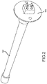
FIG. 2 is an enlarged view of the excimer bulb and the power supply ofFIG. 1 , in accordance with various embodiments; and -
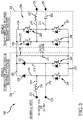
FIG. 3 is a schematic drawing illustrating features of the power supply ofFIG. 1 , in accordance with various embodiments. - The detailed description of exemplary embodiments herein makes reference to the accompanying drawings, which show exemplary embodiments by way of illustration. While these exemplary embodiments are described in sufficient detail to enable those skilled in the art to practice the exemplary embodiments of the disclosure, it should be understood that other embodiments may be realized and that logical changes and adaptations in design and construction may be made in accordance with this disclosure and the teachings herein. Thus, the detailed description herein is presented for purposes of illustration only and not limitation. The steps recited in any of the method or process descriptions may be executed in any order and are not necessarily limited to the order presented.
- Furthermore, any reference to singular includes plural embodiments, and any reference to more than one component or step may include a singular embodiment or step. Also, any reference to attached, fixed, connected or the like may include permanent, removable, temporary, partial, full and/or any other possible attachment option. Additionally, any reference to without contact (or similar phrases) may also include reduced contact or minimal contact. Surface shading lines may be used throughout the figures to denote different parts but not necessarily to denote the same or different materials.
- The present disclosure is directed to a new power supply for supplying power to an excimer lamp in aviation applications. The power supply is based on a transformer-less and analog current (AC) and direct current (DC) input compatible design. A first stage is based on a bridge-less topology that can receive a universal AC or DC input signal, may receive a relatively wide range of input signals, may provide a variable DC voltage, and may provide power factor correction with a relatively high frequency input. A second stage has a relatively high voltage full bridge based series resonant inverter that produces a relatively high voltage high frequency output signal.
- Referring now to
FIGS. 1 and2 , a portion of anaircraft lavatory 100 may include one or moreUV excimer bulb 102. Theexcimer bulb 102 may emit UV light towards a portion of thelavatory 100, as shown by an arrow 106. Thelavatory 100 may further include apower supply 104 designed to provide a power signal to theexcimer bulb 102. In particular, thepower supply 104 may provide a relatively high voltage power signal (i.e., between 500 volts and 3 kilovolts (3 kV), between 1 kV and 3 kV, or between 1.5 kV and 2.5 kV). Thepower supply 104 may be designed to receive either direct current (DC) input power or alternating current (AC) input power, and may output an AC output power signal. Thepower supply 104 may be designed to provide a desirable power signal to theexcimer bulb 102 regardless of a status of theexcimer bulb 102. That is, over time, theexcimer bulb 102 may degrade and may have changing electrical properties as a result (e.g., a resistance or capacitance of theexcimer bulb 102 may change over time). Thepower supply 104 is designed to compensate for these changing electrical properties of theexcimer bulb 102. - Referring now to
FIG. 3 , additional details of thepower supply 104 are shown. In particular, thepower supply 104 may include afirst input 200 and asecond input 202. Thefirst input 200 and thesecond input 202 may be designed to receive a DC input signal, an AC input signal, or a combined DC and AC input signal. - The
power supply 104 may include afirst stage 204, asecond stage 206, and a resonant matching network 207. Thefirst stage 204 may be referred to as a boosting stage and may apply power factor correction and power boosting to the input signal. The specific design of thefirst stage 204 is designed to handle both DC input signals and AC input signals. Thefirst stage 204 is also designed to handle a wide range of input signals. Thefirst stage 204 is also designed to provide a variable DC boosted voltage, and to provide a power factor correction to an input signal having a relatively high frequency (e.g., it may provide power factor correction to input signals having frequencies between 100 hertz (100 Hz) and 1.5 kilohertz (1.5 kHz), between 200 Hz and 1 kHz, or between 400 Hz and 900 Hz. - The
second stage 206 may be designed to function as a resonant inverter. In that regard, the resonant inverter may include afull bridge circuit 208. Thefull bridge circuit 208 may include multiple switches (as described below) that may be independently controlled to cause the output power signal to have a desirable waveform. - Notably, the second stage 206 (and the first stage 204) may perform their functions without use of a transformer. This provides several benefits such as allowing the
power supply 104 to function with a relatively large range of power input and output signals. In particular, power semiconductors used in the power supply may handle relatively high current power signals, which transformers are incapable of handling. Additional benefits of thepower supply 104 include the ability to handle both AC input signals and DC input signals. In particular, thepower supply 104 may handle input signals ranging from, for example, 28 V of DC power to 110 V of AC power. Thepower supply 104 may also provide the benefit of being compatible with AC input signals having relatively high frequencies (e.g., between 400 Hz and 900 Hz), allowing thepower supply 104 to function as a wide bandgap device. Thepower supply 104 is also capable of providing relatively high efficiency with respect to variable DC voltages (i.e., relatively low loss across the range of input DC voltages), and relatively high efficiency due to the lack of transformer and a reduced quantity of power stages relative to other power supplies. - The
first stage 204 may include afirst input line 210 coupled to thefirst input 200, and asecond input line 212 coupled to thesecond input 202. Thefirst stage 204 may also include a first stage firstparallel line 214, a first stage secondparallel line 216, and a first stage third parallel line 218. The first stage firstparallel line 214, the first stage secondparallel line 216, and the first stage third parallel line 218 may each be coupled in parallel between apositive rail 220 and anegative rail 222. - A first stage
first switch 224 may be positioned on the first stage firstparallel line 214 between thefirst input line 210 and thenegative rail 222, and a first stagesecond switch 226 may be positioned on the first stage secondparallel line 216 between thesecond input line 212 and thenegative rail 222. The first stagefirst switch 224 and the first stagesecond switch 226 may each include a power transistor, such as a metal-oxide-semiconductor field-effect transistor (MOSFET), a diode, or the like. A controller (not shown) may control operation of theswitches positive rail 220 and thenegative rail 222. - The
first stage 204 may further include afirst switch 228 positioned in the first stage firstparallel line 214 and coupled between thefirst input line 210 and thepositive rail 220, and asecond switch 230 positioned on the first stage secondparallel line 216 and coupled between thesecond input line 212 and thepositive rail 220. Theswitches diodes positive rail 220, and anodes coupled to thefirst input line 210 and thesecond input line 212, respectively. - The
first stage 204 may also include afirst inductor 232 positioned on thefirst input line 210 and coupled between thefirst input 200 and the first stage firstparallel line 214. Thefirst stage 204 may also include a second inductor 233 positioned on thesecond input line 212 and coupled between thesecond input 202 and the first stage secondparallel line 216. Thefirst stage 204 may further include afirst capacitor 234 positioned on the first stage third parallel line 218 and coupled between thepositive rail 220 and thenegative rail 222. - The
second stage 206, as referenced above, may include thefull bridge circuit 208 coupled between thepositive rail 220 and thenegative rail 222. That is, a first signal may be received at thesecond stage 206 on thepositive rail 220, and a second signal may be received at thesecond stage 206 on thenegative rail 222. - The
full bridge circuit 208 may include a second stage firstparallel line 236 and a second stage secondparallel line 238 each coupled in parallel between thepositive rail 220 and thenegative rail 222. Afirst output line 240 may be coupled to the second stage firstparallel line 236 and may provide a first output signal to afirst output terminal 256, and asecond output line 242 may be coupled to the second stage secondparallel line 238 and may provide a second output signal to asecond output terminal 258. - The
full bridge circuit 208 may further include a first linefirst switch 244 positioned on the second stage firstparallel line 236 and coupled between thepositive rail 220 and thefirst output line 240. Thefull bridge circuit 208 may further include a first linesecond switch 246 positioned on the second stage firstparallel line 236 and coupled between thefirst output line 240 and thenegative rail 222. Thefull bridge circuit 208 may also include a second linefirst switch 248 positioned on the second stage secondparallel line 238 and coupled between thepositive rail 220 and thesecond output line 242. Thefull bridge circuit 208 may further include a second linesecond switch 250 positioned on the second stage secondparallel line 238 and coupled between thesecond output line 242 and thenegative rail 222. - The resonant matching network 207 may include various combinations of inductors and capacitors. The resonant matching network 207 may be a second order (LC), a third order (LCL), or other cascaded combination of capacitors, inductors, and resistors to minimize the size and match the impedance characteristics of the UC lamp.
- Benefits and other advantages have been described herein with regard to specific embodiments. Furthermore, the connecting lines shown in the various figures contained herein are intended to represent exemplary functional relationships and/or physical couplings between the various elements. It should be noted that many alternative or additional functional relationships or physical connections may be present in a practical system. However, the benefits, advantages, and any elements that may cause any benefit or advantage to occur or become more pronounced are not to be construed as critical, required, or essential features or elements of the disclosure. The scope of the disclosure is accordingly to be limited by nothing other than the appended claims, in which reference to an element in the singular is not intended to mean "one and only one" unless explicitly so stated, but rather "one or more." Moreover, where a phrase similar to "at least one of A, B, or C" is used in the claims, it is intended that the phrase be interpreted to mean that A alone may be present in an embodiment, B alone may be present in an embodiment, C alone may be present in an embodiment, or that any combination of the elements A, B and C may be present in a single embodiment; for example, A and B, A and C, B and C, or A and B and C.
- Systems, methods and apparatus are provided herein. In the detailed description herein, references to "various embodiments", "one embodiment", "an embodiment", "an example embodiment", etc., indicate that the embodiment described may include a particular feature, structure, or characteristic, but every embodiment may not necessarily include the particular feature, structure, or characteristic. Moreover, such phrases are not necessarily referring to the same embodiment. Further, when a particular feature, structure, or characteristic is described in connection with an embodiment, it is submitted that it is within the knowledge of one skilled in the art to affect such feature, structure, or characteristic in connection with other embodiments whether or not explicitly described. After reading the description, it will be apparent to one skilled in the relevant art(s) how to implement the disclosure in alternative embodiments.
- Furthermore, no element, component, or method step in the present disclosure is intended to be dedicated to the public regardless of whether the element, component, or method step is explicitly recited in the claims. As used herein, the terms "comprises", "comprising", or any other variation thereof, are intended to cover a non-exclusive inclusion, such that a process, method, article, or apparatus that comprises a list of elements does not include only those elements but may include other elements not expressly listed or inherent to such process, method, article, or apparatus.
Claims (15)
- A system for use in generating a power signal, the system comprising:a first stage circuit (204) having:a first input line (210) coupled to a first stage first parallel line (214) having a first stage first switch (224) positioned thereon,a second input line (212) coupled to a first stage second parallel line having a first stage second switch (226) positioned thereon, anda first stage third parallel line (218) oriented in parallel with the first stage first parallel line and the first stage second parallel line between a positive rail (220) and a negative rail (222), the first stage third parallel line having a first capacitor (234) positioned thereon; anda second stage circuit (206) having a resonant inverter coupled between the positive rail and the negative rail and configured to output the power signal.
- The system of claim 1, further comprising:a first diode coupled between the first input line and the positive rail; anda second diode coupled between the second input line and the positive rail,wherein:the first stage first switch (224) is coupled between the first input line and the negative rail, andthe first stage second switch (226) is coupled between the second input line and the negative rail.
- The system of claim 2, wherein:the first diode has a first anode coupled to the first input line and a first cathode coupled to the positive rail; andthe second diode has a second anode coupled to the second input line and a second cathode coupled to the positive rail.
- The system of claim 3, wherein the first stage first switch (224) and the first stage second switch (226) each include a transistor.
- The system of claim 3, further comprising a first inductor (232) positioned on the first input line.
- The system of claim 5, wherein the resonant inverter includes a full bridge circuit (208).
- The system of claim 6, wherein the full bridge circuit (208) includes:a second stage first parallel line (236) coupled between the positive rail and the negative rail;a second stage second parallel line (238) coupled between the positive rail and the negative rail;a first output line (240) coupled to the second stage first parallel line; anda second output line (242) coupled to the second stage second parallel line.
- The system of claim 7, wherein the full bridge circuit (208) further includes:a first line first switch (244) coupled between the first output line and the positive rail;a first line second switch (246) coupled between the first output line and the negative rail;a second line first switch (248) coupled between the second output line and the positive rail; anda second line second switch (250) coupled between the second output line and the negative rail.
- The system of claim 8, further comprising:a second inductor positioned on the first output line (240); anda second capacitor positioned on the second output line (242).
- The system of claim 1, wherein the system operates as a power supply for an excimer bulb, and preferably wherein the system provides the power signal for the excimer bulb and lacks a transformer.
- A system for use in generating a power signal for powering an excimer bulb, the system comprising:a first input line (210) coupled to a first stage first parallel line (214);a second input line (212) coupled to a first stage second parallel line (216), the first stage first parallel line and the first stage second parallel line coupled in parallel between a positive rail (220) and a negative rail (222);a first stage first switch (224) positioned on the first stage first parallel line and coupled between the first input line and the negative rail;a first stage second switch (226) positioned on the first stage second parallel line and coupled between the second input line and the negative rail; anda second stage circuit (206) having a full bridge circuit (208) coupled between the positive rail and the negative rail and configured to output the power signal.
- The system of claim 11, further comprising:a first inductor positioned on the first input line;a first stage third parallel line (218) coupled between the positive rail and the negative rail; anda first capacitor positioned on the first stage third parallel line.
- The system of claim 12, further comprising:a first diode coupled between the first input line and the positive rail; anda second diode coupled between the second input line and the positive rail, and preferably wherein the full bridge circuit (208) includes:a second stage first parallel line (236) coupled between the positive rail and the negative rail;a second stage second parallel line (238) coupled between the positive rail and the negative rail;a first output line (240) coupled to the second stage first parallel line; anda second output line (242) coupled to the second stage second parallel line, and preferably wherein the full bridge circuit further includes:a first line first switch (244) coupled between the first output line and the positive rail;a first line second switch (246) coupled between the first output line and the negative rail;a second line first switch (248) coupled between the second output line and the positive rail; anda second line second switch (250) coupled between the second output line and the negative rail, and more preferably further comprising:a second inductor positioned on the first output line; anda second capacitor positioned on the second output line.
- A system for use in generating a power signal for powering an excimer bulb, the system comprising:a first input line (210) coupled to a first stage first parallel line (214);a second input line (212) coupled to a first stage second parallel line (216), the first stage first parallel line and the first stage second parallel line coupled in parallel between a positive rail and a negative rail;a first stage third parallel line (218) coupled between the positive rail and the negative rail;a first capacitor positioned on the first stage third parallel line;a first inductor positioned on the first input line;a first stage first switch (224) positioned on the first stage first parallel line and coupled between the first input line and the negative rail;a first stage second switch (226) positioned on the first stage second parallel line and coupled between the second input line and the negative rail;a second stage circuit (206) having a full bridge circuit (208) coupled between the positive rail (220) and the negative rail (222) and configured to output the power signal;a first output line (240) having a second inductor positioned thereon; anda second output line (242) having a second capacitor positioned thereon.
- The system of claim 14, wherein the full bridge circuit (208) includes:a second stage first parallel line (236) coupled between the positive rail and the negative rail; anda second stage second parallel line (238) coupled between the positive rail and the negative rail;wherein:the first output line (240) is coupled to the second stage first parallel line andthe second output line (242) is coupled to the second stage second parallel line;and preferably wherein the full bridge circuit (208) further includes:a first line first switch (244) coupled between the first output line and the positive rail;a first line second switch (246) coupled between the first output line and the negative rail;a second line first switch (248) coupled between the second output line and the positive rail; anda second line second switch (250) coupled between the second output line and the negative rail.
Applications Claiming Priority (1)
| Application Number | Priority Date | Filing Date | Title |
|---|---|---|---|
| US17/336,086 US11843323B2 (en) | 2021-06-01 | 2021-06-01 | Transformer-less AC-DC input compatible boost resonant inverter |
Publications (1)
| Publication Number | Publication Date |
|---|---|
| EP4099550A1 true EP4099550A1 (en) | 2022-12-07 |
Family
ID=81580554
Family Applications (1)
| Application Number | Title | Priority Date | Filing Date |
|---|---|---|---|
| EP22171661.6A Pending EP4099550A1 (en) | 2021-06-01 | 2022-05-04 | Transformer-less ac-dc input compatible boost resonant inverter |
Country Status (2)
| Country | Link |
|---|---|
| US (1) | US11843323B2 (en) |
| EP (1) | EP4099550A1 (en) |
Citations (2)
| Publication number | Priority date | Publication date | Assignee | Title |
|---|---|---|---|---|
| US20050237010A1 (en) * | 2004-04-26 | 2005-10-27 | Delta Electronics Inc. | Architecture of power supply system for LCD apparatus |
| DE102014114248A1 (en) * | 2014-09-30 | 2016-03-31 | Sma Solar Technology Ag | Power generation plant and method for operating an inverter |
Family Cites Families (4)
| Publication number | Priority date | Publication date | Assignee | Title |
|---|---|---|---|---|
| US6107756A (en) | 1997-07-25 | 2000-08-22 | Parra; Jorge M. | Low-voltage non-thermionic ballast-free energy-efficient gas-discharge landscape lighting system and method using high-frequency square wave AC driver circuits |
| US7009347B2 (en) | 2004-01-20 | 2006-03-07 | Nicollet Technologies Corporation | Multiple discharge load electronic ballast system |
| WO2018194673A1 (en) * | 2017-04-21 | 2018-10-25 | Abb Schweiz Ag | Converter system for powering an electrical load |
| US10668178B2 (en) * | 2018-03-21 | 2020-06-02 | The Boeing Company | Systems and methods for powering a load |
-
2021
- 2021-06-01 US US17/336,086 patent/US11843323B2/en active Active
-
2022
- 2022-05-04 EP EP22171661.6A patent/EP4099550A1/en active Pending
Patent Citations (2)
| Publication number | Priority date | Publication date | Assignee | Title |
|---|---|---|---|---|
| US20050237010A1 (en) * | 2004-04-26 | 2005-10-27 | Delta Electronics Inc. | Architecture of power supply system for LCD apparatus |
| DE102014114248A1 (en) * | 2014-09-30 | 2016-03-31 | Sma Solar Technology Ag | Power generation plant and method for operating an inverter |
Non-Patent Citations (6)
| Title |
|---|
| DARLY S S ET AL: "A novel dual boost rectifier for power factor improvement", ELECTRICAL ENERGY SYSTEMS (ICEES), 2011 1ST INTERNATIONAL CONFERENCE ON, IEEE, 3 January 2011 (2011-01-03), pages 122 - 127, XP031923405, ISBN: 978-1-4244-9732-4, DOI: 10.1109/ICEES.2011.5725314 * |
| HU JIN ET AL: "Flexible resonant tank for a combined converter to achieve an HPS and LED compatible driver", FRONTIERS OF INFORMATION TECHNOLOGY & ELECTRONIC ENGINEERING, ZHEJIANG UNIVERSITY PRESS, HEIDELBERG, vol. 16, no. 8, 8 August 2015 (2015-08-08), pages 679 - 693, XP035527205, ISSN: 2095-9184, [retrieved on 20150808], DOI: 10.1631/FITEE.1500054 * |
| MAHMOUD M I ET AL: "DESIGN PARAMETERS FOR HIGH FREQUENCY SERIES RESONANCE ENERGY CONVERTERS USED AS FLUORESCENT LAMP ELECTRONIC BALLAST", PROCEEDINGS OF THE EUROPEAN CONFERENCE ON POWER ELECTRONICS AND APPLICATIONS. (EPE). AACHEN, 9 - 12 OCTOBER, 1989, DUSSELDORF, EPE SECRETARIAT, DE, vol. 1, 9 October 1989 (1989-10-09), pages 367 - 371, XP000143419 * |
| SPIAZZI G ET AL: "Non iterative design procedure of LCC-based electronic ballasts for fluorescent lamps including dimming operation", ENERGY CONVERSION CONGRESS AND EXPOSITION, 2009. ECCE. IEEE, IEEE, PISCATAWAY, NJ, USA, 20 September 2009 (2009-09-20), pages 2065 - 2072, XP031888050, ISBN: 978-1-4244-2893-9, DOI: 10.1109/ECCE.2009.5316571 * |
| SUJA C RAJAPPAN ET AL: "An efficient bridgeless power factor correction boost converter", INTELLIGENT SYSTEMS AND CONTROL (ISCO), 2013 7TH INTERNATIONAL CONFERENCE ON, IEEE, 4 January 2013 (2013-01-04), pages 55 - 59, XP032344426, ISBN: 978-1-4673-4359-6, DOI: 10.1109/ISCO.2013.6481122 * |
| TSORNG-JUU LIANG ET AL: "Interleaving Controlled Three-Leg Electronic Ballast for Dual-HID-Lamps", IEEE TRANSACTIONS ON POWER ELECTRONICS, INSTITUTE OF ELECTRICAL AND ELECTRONICS ENGINEERS, USA, vol. 23, no. 3, 1 May 2008 (2008-05-01), pages 1401 - 1409, XP011207116, ISSN: 0885-8993 * |
Also Published As
| Publication number | Publication date |
|---|---|
| US20220385205A1 (en) | 2022-12-01 |
| US11843323B2 (en) | 2023-12-12 |
Similar Documents
| Publication | Publication Date | Title |
|---|---|---|
| US9907130B2 (en) | High-efficiency LED driver and driving method | |
| US9906169B1 (en) | DC-AC conversion circuit having a first double ended DC pulse stage and a second AC stage | |
| US7432661B2 (en) | Electronic ballast having a flyback cat-ear power supply | |
| TW347642B (en) | Ballast system | |
| WO1995010930A1 (en) | Integrated electronic energy converter | |
| CN1113101A (en) | Parallel resonant ballast with boost | |
| US8569973B2 (en) | Power supply for lamps, particularly for LED-MR16 lamps | |
| US9369060B2 (en) | Power generation system and package | |
| US20050007034A1 (en) | Discharge power supply apparatus | |
| US11843323B2 (en) | Transformer-less AC-DC input compatible boost resonant inverter | |
| US7791905B2 (en) | Electrical DC-DC power converter with magnetically coupled switch control circuit | |
| US11411510B2 (en) | DC/AC inverter resonance topology | |
| WO2008042069A2 (en) | Circuit for powering a high intensity discharge lamp | |
| Lee et al. | LED driver with TRIAC dimming control by variable switched capacitance for power regulation | |
| US12501532B2 (en) | Redundant lighting driver system | |
| JP2006529050A (en) | Light-adjustable gas discharge lamp illumination system with series cold cathode activation | |
| US20160262250A1 (en) | Power generation system and package | |
| JP2000208289A (en) | Discharge lamp lighting device | |
| CN120729060A (en) | An isolated boost circuit suitable for new energy and power products | |
| Nayak et al. | Soft-switched Single-stage Isolated AC-DC Converter for High Power Applications | |
| GB2472038A (en) | Power adaptor for discharge light source | |
| JP2005124369A (en) | High frequency inverter device and discharge lamp lighting device | |
| JPH0515395U (en) | lighting equipment | |
| JP2012221845A (en) | Discharge lamp turn-on device and luminaire | |
| KR20180129363A (en) | Plasma power supply operable in wide range |
Legal Events
| Date | Code | Title | Description |
|---|---|---|---|
| PUAI | Public reference made under article 153(3) epc to a published international application that has entered the european phase |
Free format text: ORIGINAL CODE: 0009012 |
|
| STAA | Information on the status of an ep patent application or granted ep patent |
Free format text: STATUS: THE APPLICATION HAS BEEN PUBLISHED |
|
| AK | Designated contracting states |
Kind code of ref document: A1 Designated state(s): AL AT BE BG CH CY CZ DE DK EE ES FI FR GB GR HR HU IE IS IT LI LT LU LV MC MK MT NL NO PL PT RO RS SE SI SK SM TR |
|
| STAA | Information on the status of an ep patent application or granted ep patent |
Free format text: STATUS: REQUEST FOR EXAMINATION WAS MADE |
|
| 17P | Request for examination filed |
Effective date: 20230606 |
|
| RBV | Designated contracting states (corrected) |
Designated state(s): AL AT BE BG CH CY CZ DE DK EE ES FI FR GB GR HR HU IE IS IT LI LT LU LV MC MK MT NL NO PL PT RO RS SE SI SK SM TR |
|
| P01 | Opt-out of the competence of the unified patent court (upc) registered |
Effective date: 20230922 |
|
| STAA | Information on the status of an ep patent application or granted ep patent |
Free format text: STATUS: EXAMINATION IS IN PROGRESS |
|
| 17Q | First examination report despatched |
Effective date: 20240123 |