EP4099401B1 - Rückkontaktstruktur und vergrabene solarzelle mit selektiver kontaktregion damit - Google Patents
Rückkontaktstruktur und vergrabene solarzelle mit selektiver kontaktregion damit Download PDFInfo
- Publication number
- EP4099401B1 EP4099401B1 EP21000195.4A EP21000195A EP4099401B1 EP 4099401 B1 EP4099401 B1 EP 4099401B1 EP 21000195 A EP21000195 A EP 21000195A EP 4099401 B1 EP4099401 B1 EP 4099401B1
- Authority
- EP
- European Patent Office
- Prior art keywords
- layer
- dielectric layer
- silicon
- doped
- recesses
- Prior art date
- Legal status (The legal status is an assumption and is not a legal conclusion. Google has not performed a legal analysis and makes no representation as to the accuracy of the status listed.)
- Active
Links
- XUIMIQQOPSSXEZ-UHFFFAOYSA-N Silicon Chemical compound [Si] XUIMIQQOPSSXEZ-UHFFFAOYSA-N 0.000 claims description 178
- 229910052710 silicon Inorganic materials 0.000 claims description 178
- 239000010703 silicon Substances 0.000 claims description 178
- 239000000758 substrate Substances 0.000 claims description 145
- HBMJWWWQQXIZIP-UHFFFAOYSA-N silicon carbide Chemical compound [Si+]#[C-] HBMJWWWQQXIZIP-UHFFFAOYSA-N 0.000 claims description 126
- 229910010271 silicon carbide Inorganic materials 0.000 claims description 110
- 229910021417 amorphous silicon Inorganic materials 0.000 claims description 77
- VYPSYNLAJGMNEJ-UHFFFAOYSA-N Silicium dioxide Chemical compound O=[Si]=O VYPSYNLAJGMNEJ-UHFFFAOYSA-N 0.000 claims description 69
- 229910052814 silicon oxide Inorganic materials 0.000 claims description 55
- TWNQGVIAIRXVLR-UHFFFAOYSA-N oxo(oxoalumanyloxy)alumane Chemical compound O=[Al]O[Al]=O TWNQGVIAIRXVLR-UHFFFAOYSA-N 0.000 claims description 38
- 229910052581 Si3N4 Inorganic materials 0.000 claims description 32
- HQVNEWCFYHHQES-UHFFFAOYSA-N silicon nitride Chemical compound N12[Si]34N5[Si]62N3[Si]51N64 HQVNEWCFYHHQES-UHFFFAOYSA-N 0.000 claims description 32
- 229910021420 polycrystalline silicon Inorganic materials 0.000 claims description 31
- 238000000034 method Methods 0.000 claims description 30
- 230000008569 process Effects 0.000 claims description 21
- RYGMFSIKBFXOCR-UHFFFAOYSA-N Copper Chemical compound [Cu] RYGMFSIKBFXOCR-UHFFFAOYSA-N 0.000 claims description 19
- 229910052802 copper Inorganic materials 0.000 claims description 19
- 239000010949 copper Substances 0.000 claims description 19
- 229910052751 metal Inorganic materials 0.000 claims description 14
- 239000002184 metal Substances 0.000 claims description 14
- 229910052782 aluminium Inorganic materials 0.000 claims description 13
- XAGFODPZIPBFFR-UHFFFAOYSA-N aluminium Chemical compound [Al] XAGFODPZIPBFFR-UHFFFAOYSA-N 0.000 claims description 13
- 230000007423 decrease Effects 0.000 claims description 11
- ORUIBWPALBXDOA-UHFFFAOYSA-L magnesium fluoride Chemical compound [F-].[F-].[Mg+2] ORUIBWPALBXDOA-UHFFFAOYSA-L 0.000 claims description 10
- 229910001635 magnesium fluoride Inorganic materials 0.000 claims description 10
- 230000005684 electric field Effects 0.000 claims description 8
- 238000007667 floating Methods 0.000 claims description 8
- BQCADISMDOOEFD-UHFFFAOYSA-N Silver Chemical compound [Ag] BQCADISMDOOEFD-UHFFFAOYSA-N 0.000 claims description 3
- 238000009713 electroplating Methods 0.000 claims description 3
- 238000005240 physical vapour deposition Methods 0.000 claims description 3
- 229910052709 silver Inorganic materials 0.000 claims description 3
- 239000004332 silver Substances 0.000 claims description 3
- 238000009792 diffusion process Methods 0.000 description 35
- 238000002161 passivation Methods 0.000 description 34
- 230000000694 effects Effects 0.000 description 32
- 239000000969 carrier Substances 0.000 description 30
- 238000000151 deposition Methods 0.000 description 30
- 238000002360 preparation method Methods 0.000 description 23
- 230000005641 tunneling Effects 0.000 description 19
- IJGRMHOSHXDMSA-UHFFFAOYSA-N Atomic nitrogen Chemical compound N#N IJGRMHOSHXDMSA-UHFFFAOYSA-N 0.000 description 18
- 230000008021 deposition Effects 0.000 description 17
- 238000003079 width control Methods 0.000 description 17
- 239000007789 gas Substances 0.000 description 13
- 238000004519 manufacturing process Methods 0.000 description 12
- ZOXJGFHDIHLPTG-UHFFFAOYSA-N Boron Chemical compound [B] ZOXJGFHDIHLPTG-UHFFFAOYSA-N 0.000 description 10
- OAICVXFJPJFONN-UHFFFAOYSA-N Phosphorus Chemical compound [P] OAICVXFJPJFONN-UHFFFAOYSA-N 0.000 description 10
- 229910052796 boron Inorganic materials 0.000 description 10
- 229910052698 phosphorus Inorganic materials 0.000 description 10
- 239000011574 phosphorus Substances 0.000 description 10
- 238000000926 separation method Methods 0.000 description 10
- 238000002425 crystallisation Methods 0.000 description 9
- 230000008025 crystallization Effects 0.000 description 9
- 150000002500 ions Chemical class 0.000 description 9
- 229910052757 nitrogen Inorganic materials 0.000 description 9
- 239000000243 solution Substances 0.000 description 9
- 238000001039 wet etching Methods 0.000 description 9
- GYHNNYVSQQEPJS-UHFFFAOYSA-N Gallium Chemical compound [Ga] GYHNNYVSQQEPJS-UHFFFAOYSA-N 0.000 description 8
- 229910052785 arsenic Inorganic materials 0.000 description 8
- RQNWIZPPADIBDY-UHFFFAOYSA-N arsenic atom Chemical compound [As] RQNWIZPPADIBDY-UHFFFAOYSA-N 0.000 description 8
- 229910052733 gallium Inorganic materials 0.000 description 8
- 238000006243 chemical reaction Methods 0.000 description 7
- 230000003647 oxidation Effects 0.000 description 7
- 238000007254 oxidation reaction Methods 0.000 description 7
- 239000012670 alkaline solution Substances 0.000 description 6
- ILAHWRKJUDSMFH-UHFFFAOYSA-N boron tribromide Chemical compound BrB(Br)Br ILAHWRKJUDSMFH-UHFFFAOYSA-N 0.000 description 6
- 230000001965 increasing effect Effects 0.000 description 6
- 230000003287 optical effect Effects 0.000 description 6
- XHXFXVLFKHQFAL-UHFFFAOYSA-N phosphoryl trichloride Chemical compound ClP(Cl)(Cl)=O XHXFXVLFKHQFAL-UHFFFAOYSA-N 0.000 description 6
- WGTYBPLFGIVFAS-UHFFFAOYSA-M tetramethylammonium hydroxide Chemical compound [OH-].C[N+](C)(C)C WGTYBPLFGIVFAS-UHFFFAOYSA-M 0.000 description 6
- UFHFLCQGNIYNRP-UHFFFAOYSA-N Hydrogen Chemical compound [H][H] UFHFLCQGNIYNRP-UHFFFAOYSA-N 0.000 description 5
- 239000002253 acid Substances 0.000 description 5
- 239000001257 hydrogen Substances 0.000 description 5
- 229910052739 hydrogen Inorganic materials 0.000 description 5
- 230000031700 light absorption Effects 0.000 description 5
- 239000000463 material Substances 0.000 description 5
- KWYUFKZDYYNOTN-UHFFFAOYSA-M Potassium hydroxide Chemical compound [OH-].[K+] KWYUFKZDYYNOTN-UHFFFAOYSA-M 0.000 description 4
- 238000010521 absorption reaction Methods 0.000 description 4
- UORVGPXVDQYIDP-UHFFFAOYSA-N borane Chemical compound B UORVGPXVDQYIDP-UHFFFAOYSA-N 0.000 description 4
- 239000012159 carrier gas Substances 0.000 description 4
- 238000011065 in-situ storage Methods 0.000 description 4
- 239000000203 mixture Substances 0.000 description 4
- 239000001301 oxygen Substances 0.000 description 4
- 229910052760 oxygen Inorganic materials 0.000 description 4
- 229920002120 photoresistant polymer Polymers 0.000 description 4
- 238000004528 spin coating Methods 0.000 description 4
- 239000000126 substance Substances 0.000 description 4
- 238000004140 cleaning Methods 0.000 description 3
- 238000011066 ex-situ storage Methods 0.000 description 3
- 239000012535 impurity Substances 0.000 description 3
- 229910021424 microcrystalline silicon Inorganic materials 0.000 description 3
- 230000003071 parasitic effect Effects 0.000 description 3
- NTIZESTWPVYFNL-UHFFFAOYSA-N Methyl isobutyl ketone Chemical compound CC(C)CC(C)=O NTIZESTWPVYFNL-UHFFFAOYSA-N 0.000 description 2
- PXHVJJICTQNCMI-UHFFFAOYSA-N Nickel Chemical compound [Ni] PXHVJJICTQNCMI-UHFFFAOYSA-N 0.000 description 2
- XYFCBTPGUUZFHI-UHFFFAOYSA-N Phosphine Chemical compound P XYFCBTPGUUZFHI-UHFFFAOYSA-N 0.000 description 2
- 239000003929 acidic solution Substances 0.000 description 2
- 230000009286 beneficial effect Effects 0.000 description 2
- 229910000085 borane Inorganic materials 0.000 description 2
- 239000005388 borosilicate glass Substances 0.000 description 2
- 238000011109 contamination Methods 0.000 description 2
- 230000002708 enhancing effect Effects 0.000 description 2
- 238000002474 experimental method Methods 0.000 description 2
- 239000005360 phosphosilicate glass Substances 0.000 description 2
- 238000002203 pretreatment Methods 0.000 description 2
- 230000035484 reaction time Effects 0.000 description 2
- FAQYAMRNWDIXMY-UHFFFAOYSA-N trichloroborane Chemical compound ClB(Cl)Cl FAQYAMRNWDIXMY-UHFFFAOYSA-N 0.000 description 2
- XLYOFNOQVPJJNP-UHFFFAOYSA-N water Substances O XLYOFNOQVPJJNP-UHFFFAOYSA-N 0.000 description 2
- VYZAMTAEIAYCRO-UHFFFAOYSA-N Chromium Chemical compound [Cr] VYZAMTAEIAYCRO-UHFFFAOYSA-N 0.000 description 1
- RTAQQCXQSZGOHL-UHFFFAOYSA-N Titanium Chemical compound [Ti] RTAQQCXQSZGOHL-UHFFFAOYSA-N 0.000 description 1
- QVGXLLKOCUKJST-UHFFFAOYSA-N atomic oxygen Chemical compound [O] QVGXLLKOCUKJST-UHFFFAOYSA-N 0.000 description 1
- 230000004888 barrier function Effects 0.000 description 1
- 230000005540 biological transmission Effects 0.000 description 1
- 230000000903 blocking effect Effects 0.000 description 1
- 238000006388 chemical passivation reaction Methods 0.000 description 1
- 239000003795 chemical substances by application Substances 0.000 description 1
- 229910052804 chromium Inorganic materials 0.000 description 1
- 239000011651 chromium Substances 0.000 description 1
- 238000004891 communication Methods 0.000 description 1
- 239000002131 composite material Substances 0.000 description 1
- 150000001875 compounds Chemical class 0.000 description 1
- 230000007797 corrosion Effects 0.000 description 1
- 238000005260 corrosion Methods 0.000 description 1
- 239000013078 crystal Substances 0.000 description 1
- 229910021419 crystalline silicon Inorganic materials 0.000 description 1
- 230000003247 decreasing effect Effects 0.000 description 1
- 230000007547 defect Effects 0.000 description 1
- 238000005137 deposition process Methods 0.000 description 1
- 238000010586 diagram Methods 0.000 description 1
- 238000009826 distribution Methods 0.000 description 1
- 238000001312 dry etching Methods 0.000 description 1
- 238000001035 drying Methods 0.000 description 1
- 238000005516 engineering process Methods 0.000 description 1
- 230000005669 field effect Effects 0.000 description 1
- 238000000608 laser ablation Methods 0.000 description 1
- 238000004093 laser heating Methods 0.000 description 1
- 230000007246 mechanism Effects 0.000 description 1
- 238000012986 modification Methods 0.000 description 1
- 230000004048 modification Effects 0.000 description 1
- 229910021421 monocrystalline silicon Inorganic materials 0.000 description 1
- 229910052759 nickel Inorganic materials 0.000 description 1
- 239000002245 particle Substances 0.000 description 1
- 238000003359 percent control normalization Methods 0.000 description 1
- 238000005554 pickling Methods 0.000 description 1
- 238000000623 plasma-assisted chemical vapour deposition Methods 0.000 description 1
- 238000007747 plating Methods 0.000 description 1
- 239000010453 quartz Substances 0.000 description 1
- 230000005855 radiation Effects 0.000 description 1
- 239000000376 reactant Substances 0.000 description 1
- 230000009467 reduction Effects 0.000 description 1
- 238000002310 reflectometry Methods 0.000 description 1
- 239000004065 semiconductor Substances 0.000 description 1
- 238000012360 testing method Methods 0.000 description 1
- 239000010936 titanium Substances 0.000 description 1
- 229910052719 titanium Inorganic materials 0.000 description 1
- 238000012546 transfer Methods 0.000 description 1
- WFKWXMTUELFFGS-UHFFFAOYSA-N tungsten Chemical compound [W] WFKWXMTUELFFGS-UHFFFAOYSA-N 0.000 description 1
- 229910052721 tungsten Inorganic materials 0.000 description 1
- 239000010937 tungsten Substances 0.000 description 1
Images


Classifications
-
- H—ELECTRICITY
- H01—ELECTRIC ELEMENTS
- H01L—SEMICONDUCTOR DEVICES NOT COVERED BY CLASS H10
- H01L31/00—Semiconductor devices sensitive to infrared radiation, light, electromagnetic radiation of shorter wavelength or corpuscular radiation and specially adapted either for the conversion of the energy of such radiation into electrical energy or for the control of electrical energy by such radiation; Processes or apparatus specially adapted for the manufacture or treatment thereof or of parts thereof; Details thereof
- H01L31/02—Details
- H01L31/0224—Electrodes
- H01L31/022408—Electrodes for devices characterised by at least one potential jump barrier or surface barrier
- H01L31/022425—Electrodes for devices characterised by at least one potential jump barrier or surface barrier for solar cells
- H01L31/022441—Electrode arrangements specially adapted for back-contact solar cells
-
- H—ELECTRICITY
- H01—ELECTRIC ELEMENTS
- H01L—SEMICONDUCTOR DEVICES NOT COVERED BY CLASS H10
- H01L31/00—Semiconductor devices sensitive to infrared radiation, light, electromagnetic radiation of shorter wavelength or corpuscular radiation and specially adapted either for the conversion of the energy of such radiation into electrical energy or for the control of electrical energy by such radiation; Processes or apparatus specially adapted for the manufacture or treatment thereof or of parts thereof; Details thereof
- H01L31/04—Semiconductor devices sensitive to infrared radiation, light, electromagnetic radiation of shorter wavelength or corpuscular radiation and specially adapted either for the conversion of the energy of such radiation into electrical energy or for the control of electrical energy by such radiation; Processes or apparatus specially adapted for the manufacture or treatment thereof or of parts thereof; Details thereof adapted as photovoltaic [PV] conversion devices
- H01L31/06—Semiconductor devices sensitive to infrared radiation, light, electromagnetic radiation of shorter wavelength or corpuscular radiation and specially adapted either for the conversion of the energy of such radiation into electrical energy or for the control of electrical energy by such radiation; Processes or apparatus specially adapted for the manufacture or treatment thereof or of parts thereof; Details thereof adapted as photovoltaic [PV] conversion devices characterised by potential barriers
- H01L31/072—Semiconductor devices sensitive to infrared radiation, light, electromagnetic radiation of shorter wavelength or corpuscular radiation and specially adapted either for the conversion of the energy of such radiation into electrical energy or for the control of electrical energy by such radiation; Processes or apparatus specially adapted for the manufacture or treatment thereof or of parts thereof; Details thereof adapted as photovoltaic [PV] conversion devices characterised by potential barriers the potential barriers being only of the PN heterojunction type
- H01L31/0745—Semiconductor devices sensitive to infrared radiation, light, electromagnetic radiation of shorter wavelength or corpuscular radiation and specially adapted either for the conversion of the energy of such radiation into electrical energy or for the control of electrical energy by such radiation; Processes or apparatus specially adapted for the manufacture or treatment thereof or of parts thereof; Details thereof adapted as photovoltaic [PV] conversion devices characterised by potential barriers the potential barriers being only of the PN heterojunction type comprising a AIVBIV heterojunction, e.g. Si/Ge, SiGe/Si or Si/SiC solar cells
- H01L31/0747—Semiconductor devices sensitive to infrared radiation, light, electromagnetic radiation of shorter wavelength or corpuscular radiation and specially adapted either for the conversion of the energy of such radiation into electrical energy or for the control of electrical energy by such radiation; Processes or apparatus specially adapted for the manufacture or treatment thereof or of parts thereof; Details thereof adapted as photovoltaic [PV] conversion devices characterised by potential barriers the potential barriers being only of the PN heterojunction type comprising a AIVBIV heterojunction, e.g. Si/Ge, SiGe/Si or Si/SiC solar cells comprising a heterojunction of crystalline and amorphous materials, e.g. heterojunction with intrinsic thin layer
-
- H—ELECTRICITY
- H01—ELECTRIC ELEMENTS
- H01L—SEMICONDUCTOR DEVICES NOT COVERED BY CLASS H10
- H01L31/00—Semiconductor devices sensitive to infrared radiation, light, electromagnetic radiation of shorter wavelength or corpuscular radiation and specially adapted either for the conversion of the energy of such radiation into electrical energy or for the control of electrical energy by such radiation; Processes or apparatus specially adapted for the manufacture or treatment thereof or of parts thereof; Details thereof
- H01L31/02—Details
- H01L31/0216—Coatings
- H01L31/02161—Coatings for devices characterised by at least one potential jump barrier or surface barrier
- H01L31/02167—Coatings for devices characterised by at least one potential jump barrier or surface barrier for solar cells
- H01L31/02168—Coatings for devices characterised by at least one potential jump barrier or surface barrier for solar cells the coatings being antireflective or having enhancing optical properties for the solar cells
-
- H—ELECTRICITY
- H01—ELECTRIC ELEMENTS
- H01L—SEMICONDUCTOR DEVICES NOT COVERED BY CLASS H10
- H01L31/00—Semiconductor devices sensitive to infrared radiation, light, electromagnetic radiation of shorter wavelength or corpuscular radiation and specially adapted either for the conversion of the energy of such radiation into electrical energy or for the control of electrical energy by such radiation; Processes or apparatus specially adapted for the manufacture or treatment thereof or of parts thereof; Details thereof
- H01L31/02—Details
- H01L31/0236—Special surface textures
- H01L31/02363—Special surface textures of the semiconductor body itself, e.g. textured active layers
-
- H—ELECTRICITY
- H01—ELECTRIC ELEMENTS
- H01L—SEMICONDUCTOR DEVICES NOT COVERED BY CLASS H10
- H01L31/00—Semiconductor devices sensitive to infrared radiation, light, electromagnetic radiation of shorter wavelength or corpuscular radiation and specially adapted either for the conversion of the energy of such radiation into electrical energy or for the control of electrical energy by such radiation; Processes or apparatus specially adapted for the manufacture or treatment thereof or of parts thereof; Details thereof
- H01L31/0248—Semiconductor devices sensitive to infrared radiation, light, electromagnetic radiation of shorter wavelength or corpuscular radiation and specially adapted either for the conversion of the energy of such radiation into electrical energy or for the control of electrical energy by such radiation; Processes or apparatus specially adapted for the manufacture or treatment thereof or of parts thereof; Details thereof characterised by their semiconductor bodies
- H01L31/0256—Semiconductor devices sensitive to infrared radiation, light, electromagnetic radiation of shorter wavelength or corpuscular radiation and specially adapted either for the conversion of the energy of such radiation into electrical energy or for the control of electrical energy by such radiation; Processes or apparatus specially adapted for the manufacture or treatment thereof or of parts thereof; Details thereof characterised by their semiconductor bodies characterised by the material
- H01L31/0264—Inorganic materials
- H01L31/028—Inorganic materials including, apart from doping material or other impurities, only elements of Group IV of the Periodic Table
-
- H—ELECTRICITY
- H01—ELECTRIC ELEMENTS
- H01L—SEMICONDUCTOR DEVICES NOT COVERED BY CLASS H10
- H01L31/00—Semiconductor devices sensitive to infrared radiation, light, electromagnetic radiation of shorter wavelength or corpuscular radiation and specially adapted either for the conversion of the energy of such radiation into electrical energy or for the control of electrical energy by such radiation; Processes or apparatus specially adapted for the manufacture or treatment thereof or of parts thereof; Details thereof
- H01L31/0248—Semiconductor devices sensitive to infrared radiation, light, electromagnetic radiation of shorter wavelength or corpuscular radiation and specially adapted either for the conversion of the energy of such radiation into electrical energy or for the control of electrical energy by such radiation; Processes or apparatus specially adapted for the manufacture or treatment thereof or of parts thereof; Details thereof characterised by their semiconductor bodies
- H01L31/0352—Semiconductor devices sensitive to infrared radiation, light, electromagnetic radiation of shorter wavelength or corpuscular radiation and specially adapted either for the conversion of the energy of such radiation into electrical energy or for the control of electrical energy by such radiation; Processes or apparatus specially adapted for the manufacture or treatment thereof or of parts thereof; Details thereof characterised by their semiconductor bodies characterised by their shape or by the shapes, relative sizes or disposition of the semiconductor regions
- H01L31/035272—Semiconductor devices sensitive to infrared radiation, light, electromagnetic radiation of shorter wavelength or corpuscular radiation and specially adapted either for the conversion of the energy of such radiation into electrical energy or for the control of electrical energy by such radiation; Processes or apparatus specially adapted for the manufacture or treatment thereof or of parts thereof; Details thereof characterised by their semiconductor bodies characterised by their shape or by the shapes, relative sizes or disposition of the semiconductor regions characterised by at least one potential jump barrier or surface barrier
- H01L31/035281—Shape of the body
-
- H—ELECTRICITY
- H01—ELECTRIC ELEMENTS
- H01L—SEMICONDUCTOR DEVICES NOT COVERED BY CLASS H10
- H01L31/00—Semiconductor devices sensitive to infrared radiation, light, electromagnetic radiation of shorter wavelength or corpuscular radiation and specially adapted either for the conversion of the energy of such radiation into electrical energy or for the control of electrical energy by such radiation; Processes or apparatus specially adapted for the manufacture or treatment thereof or of parts thereof; Details thereof
- H01L31/04—Semiconductor devices sensitive to infrared radiation, light, electromagnetic radiation of shorter wavelength or corpuscular radiation and specially adapted either for the conversion of the energy of such radiation into electrical energy or for the control of electrical energy by such radiation; Processes or apparatus specially adapted for the manufacture or treatment thereof or of parts thereof; Details thereof adapted as photovoltaic [PV] conversion devices
- H01L31/054—Optical elements directly associated or integrated with the PV cell, e.g. light-reflecting means or light-concentrating means
- H01L31/056—Optical elements directly associated or integrated with the PV cell, e.g. light-reflecting means or light-concentrating means the light-reflecting means being of the back surface reflector [BSR] type
-
- H—ELECTRICITY
- H01—ELECTRIC ELEMENTS
- H01L—SEMICONDUCTOR DEVICES NOT COVERED BY CLASS H10
- H01L31/00—Semiconductor devices sensitive to infrared radiation, light, electromagnetic radiation of shorter wavelength or corpuscular radiation and specially adapted either for the conversion of the energy of such radiation into electrical energy or for the control of electrical energy by such radiation; Processes or apparatus specially adapted for the manufacture or treatment thereof or of parts thereof; Details thereof
- H01L31/04—Semiconductor devices sensitive to infrared radiation, light, electromagnetic radiation of shorter wavelength or corpuscular radiation and specially adapted either for the conversion of the energy of such radiation into electrical energy or for the control of electrical energy by such radiation; Processes or apparatus specially adapted for the manufacture or treatment thereof or of parts thereof; Details thereof adapted as photovoltaic [PV] conversion devices
- H01L31/06—Semiconductor devices sensitive to infrared radiation, light, electromagnetic radiation of shorter wavelength or corpuscular radiation and specially adapted either for the conversion of the energy of such radiation into electrical energy or for the control of electrical energy by such radiation; Processes or apparatus specially adapted for the manufacture or treatment thereof or of parts thereof; Details thereof adapted as photovoltaic [PV] conversion devices characterised by potential barriers
- H01L31/068—Semiconductor devices sensitive to infrared radiation, light, electromagnetic radiation of shorter wavelength or corpuscular radiation and specially adapted either for the conversion of the energy of such radiation into electrical energy or for the control of electrical energy by such radiation; Processes or apparatus specially adapted for the manufacture or treatment thereof or of parts thereof; Details thereof adapted as photovoltaic [PV] conversion devices characterised by potential barriers the potential barriers being only of the PN homojunction type, e.g. bulk silicon PN homojunction solar cells or thin film polycrystalline silicon PN homojunction solar cells
- H01L31/0682—Semiconductor devices sensitive to infrared radiation, light, electromagnetic radiation of shorter wavelength or corpuscular radiation and specially adapted either for the conversion of the energy of such radiation into electrical energy or for the control of electrical energy by such radiation; Processes or apparatus specially adapted for the manufacture or treatment thereof or of parts thereof; Details thereof adapted as photovoltaic [PV] conversion devices characterised by potential barriers the potential barriers being only of the PN homojunction type, e.g. bulk silicon PN homojunction solar cells or thin film polycrystalline silicon PN homojunction solar cells back-junction, i.e. rearside emitter, solar cells, e.g. interdigitated base-emitter regions back-junction cells
-
- H—ELECTRICITY
- H01—ELECTRIC ELEMENTS
- H01L—SEMICONDUCTOR DEVICES NOT COVERED BY CLASS H10
- H01L31/00—Semiconductor devices sensitive to infrared radiation, light, electromagnetic radiation of shorter wavelength or corpuscular radiation and specially adapted either for the conversion of the energy of such radiation into electrical energy or for the control of electrical energy by such radiation; Processes or apparatus specially adapted for the manufacture or treatment thereof or of parts thereof; Details thereof
- H01L31/18—Processes or apparatus specially adapted for the manufacture or treatment of these devices or of parts thereof
- H01L31/1804—Processes or apparatus specially adapted for the manufacture or treatment of these devices or of parts thereof comprising only elements of Group IV of the Periodic Table
-
- H—ELECTRICITY
- H01—ELECTRIC ELEMENTS
- H01L—SEMICONDUCTOR DEVICES NOT COVERED BY CLASS H10
- H01L31/00—Semiconductor devices sensitive to infrared radiation, light, electromagnetic radiation of shorter wavelength or corpuscular radiation and specially adapted either for the conversion of the energy of such radiation into electrical energy or for the control of electrical energy by such radiation; Processes or apparatus specially adapted for the manufacture or treatment thereof or of parts thereof; Details thereof
- H01L31/18—Processes or apparatus specially adapted for the manufacture or treatment of these devices or of parts thereof
- H01L31/186—Particular post-treatment for the devices, e.g. annealing, impurity gettering, short-circuit elimination, recrystallisation
- H01L31/1868—Passivation
-
- Y—GENERAL TAGGING OF NEW TECHNOLOGICAL DEVELOPMENTS; GENERAL TAGGING OF CROSS-SECTIONAL TECHNOLOGIES SPANNING OVER SEVERAL SECTIONS OF THE IPC; TECHNICAL SUBJECTS COVERED BY FORMER USPC CROSS-REFERENCE ART COLLECTIONS [XRACs] AND DIGESTS
- Y02—TECHNOLOGIES OR APPLICATIONS FOR MITIGATION OR ADAPTATION AGAINST CLIMATE CHANGE
- Y02E—REDUCTION OF GREENHOUSE GAS [GHG] EMISSIONS, RELATED TO ENERGY GENERATION, TRANSMISSION OR DISTRIBUTION
- Y02E10/00—Energy generation through renewable energy sources
- Y02E10/50—Photovoltaic [PV] energy
- Y02E10/52—PV systems with concentrators
-
- Y—GENERAL TAGGING OF NEW TECHNOLOGICAL DEVELOPMENTS; GENERAL TAGGING OF CROSS-SECTIONAL TECHNOLOGIES SPANNING OVER SEVERAL SECTIONS OF THE IPC; TECHNICAL SUBJECTS COVERED BY FORMER USPC CROSS-REFERENCE ART COLLECTIONS [XRACs] AND DIGESTS
- Y02—TECHNOLOGIES OR APPLICATIONS FOR MITIGATION OR ADAPTATION AGAINST CLIMATE CHANGE
- Y02E—REDUCTION OF GREENHOUSE GAS [GHG] EMISSIONS, RELATED TO ENERGY GENERATION, TRANSMISSION OR DISTRIBUTION
- Y02E10/00—Energy generation through renewable energy sources
- Y02E10/50—Photovoltaic [PV] energy
- Y02E10/547—Monocrystalline silicon PV cells
Definitions
- the disclosure relates to the field of solar cells, and more particularly to a back contact structure and a selective contact region buried solar cell comprising the same.
- efficiency losses of the cell may be divided into two aspects, i.e., electric losses and optical losses.
- Important parts of the electric losses are composite losses and resistance losses caused by metal-semiconductor contacts, while an important part of the optical losses is a shading of metal grid lines of illuminated faces.
- US 2014/096821 A1 , US 2017/117433 A1 , KR 2013 0037395 A and US 2016/284896 A1 disclose solar cells .
- a passivated metal contact structure has remarkable electrical performance, and can obtain a low contact resistivity and low surface composition at the same time; this structure comprises an ultrathin tunneling oxide layer and an N-type doped or P-type doped polycrystalline silicon layer. Since the absorption of light by the doped polycrystalline silicon layer belongs to "parasitic" absorption, i.e., no contribution to a photo-generated current, the passivated metal contact structure is chiefly applied to a back surface of the cell, so that a front surface thoroughly avoids the shading of the metal grid lines. Solar radiation received on the solar cell generates electrons and holes; these electrons and holes are migrated to the doped polycrystalline silicon layer, to generate a voltage difference in the doped polycrystalline silicon layer.
- a solar cell is composed of the foregoing passivated metal contact structure and another passivated metal contact structure, or a solar cell is composed of the foregoing passivated metal contact structure and a diffusion structure.
- the existing passivated contact structure and the diffusion structure are directly deposited on a back of a silicon slice; however, when they are connected to each other without separation, undesirable phenomena such as electric leakage would occur.
- the passivated contact structure is separated from the diffusion structure, to prevent a cell open-circuit voltage reduction from electric leakage.
- the existing trench is prepared through laser perforation or wet etching; in this case, since the width of the existing trench is dozens of microns, and thus width control is highly required, so that the preparation is difficult.
- the passivation is performed using only a single dielectric layer; however, using the single dielectric layer for passivation has a relatively poor passivation effect and a poor inner back reflection effect.
- An objective of an embodiment of the disclosure is to provide a back contact structure of a solar cell, aiming at solving the existing problems of a high trench width control requirement and a poor passivation effect.
- the invention provides a back contact structure of a solar cell as defined by the subject-matter of claim 1, comprising
- the first doped region is a P-type doped region, and the second doped region is an N-type doped layer; or the first doped region is an N-type doped region, and the second doped region is a P-type doped layer.
- the first doped region comprises doped polycrystalline silicon, doped silicon carbide or doped amorphous silicon.
- the first dielectric layer is a tunnelling oxide layer.
- the first dielectric layer is one of a tunneling oxide layer, an intrinsic silicon carbide layer and an intrinsic amorphous silicon layer, or a combination thereof.
- the second dielectric layer is one of an aluminum oxide layer, a silicon nitride layer, a silicon oxynitride layer, an intrinsic silicon carbide layer, an intrinsic amorphous silicon layer and a silicon oxide layer, or a combination thereof.
- the second dielectric layer covers regions between the first conductive regions and the second conductive regions, or extends to cover the first conductive regions and/or the second conductive regions.
- the part of the back surface of the silicon substrate between the first conductive regions and the second conductive regions comprises a rough texture structure.
- the width of the P-type doped region is 300-600 ⁇ m, or, the width of the N-type doped region is 100-500 ⁇ m.
- the depth of each recess is 0.01-10 ⁇ m, and the horizontal distance between the first conductive regions and the second conductive regions is 0-500 ⁇ m.
- the first dielectric layer covers the first doped regions, or extends to cover regions between the first doped regions and the second doped regions.
- the recess is an arc, a trapezoid, or a square.
- the second doped region has a junction depth of 0.01-1 ⁇ m, a sheet resistance of 10-500 ohm/sqr, and a surface concentration of 1 E18-1 E21 cm -3 .
- the thickness of the first dielectric layer is 1-20 nm, and the total thickness of the plurality of first conductive regions is greater than 20 nm.
- the doped silicon carbide comprises doped hydrogenated silicon carbide.
- the first dielectric layer comprises the intrinsic silicon carbide layer.
- the tunneling oxide layer comprises one or more of a silicon oxide layer and an aluminum oxide layer.
- the intrinsic silicon carbide layer in the first dielectric layer comprises an intrinsic hydrogenated silicon carbide layer.
- the second dielectric layer comprises the aluminum oxide layer and the intrinsic silicon carbide layer or the silicon oxide layer and the intrinsic silicon carbide layer, and the thickness of the second dielectric layer is greater than 25 nm.
- the thickness of the aluminum oxide layer or the silicon oxide layer in the second dielectric layer is less than 25 nm, and the thickness of the intrinsic silicon carbide layer in the second dielectric layer is greater than 10 nm.
- the intrinsic silicon carbide layer in the second dielectric layer comprises at least one first intrinsic silicon carbide film.
- the refractive indexes of the first intrinsic silicon carbide films decrease from the back surface of the silicon substrate to outside.
- a magnesium fluoride layer is disposed at an outer layer of the second dielectric layer.
- the conductive layer is a TCO transparent conductive film and/or a metal electrode.
- the metal electrode comprises a silver electrode, a copper electrode, an aluminum electrode, a tin-clad copper electrode, or a silver-clad copper electrode.
- the copper electrode is electro-plated copper prepared through an electroplating process or a copper electrode prepared through physical vapor deposition.
- the objective of another embodiment of the disclosure is to further provide a selective contact region buried solar cell, comprising:
- the third dielectric layer is one of an aluminum oxide layer, a silicon nitride layer, a silicon oxynitride layer, a silicon carbide layer, an intrinsic amorphous silicon layer and a silicon oxide layer, or a combination thereof.
- the third dielectric layer comprises the silicon oxide layer and the silicon carbide layer or the aluminum oxide layer and the silicon carbide layer, and the thickness of the third dielectric layer is greater than 50 nm.
- the thickness of the aluminum oxide layer or the silicon oxide layer in the third dielectric layer is less than 40 nm, and the thickness of the silicon carbide layer in the third dielectric layer is greater than 10 nm.
- the silicon carbide layer in the third dielectric layer comprises at least one silicon carbide.
- the refractive indexes of different silicon carbide films decrease from the front surface of the silicon substrate to outside.
- a magnesium fluoride layer is disposed at an outer layer of the third dielectric layer.
- an electric field layer or a floating junction is further disposed between the front surface of the silicon substrate and the third dielectric layer.
- the objective of another embodiment of the disclosure is to further provide a cell assembly comprising the selective contact region buried solar cell as stated above.
- the objective of another embodiment of the disclosure is to further provide a photovoltaic system, comprising the cell assembly as stated above.
- the step of alternately preparing first conductive regions and second conductive regions on the silicon substrate comprises:
- the step of successively preparing the first dielectric layer and the first doped region having a first conductivity type inside or outside a recess comprises:
- the step of successively preparing the first dielectric layer and the first doped region having a first conductivity type inside or outside a recess comprises:
- the step of successively preparing the first dielectric layer and the first doped region having a first conductivity type inside or outside a recess comprises:
- the step of preparing the second doped region having a second conductivity type outside or inside the corresponding recess which is not exclusively directed to manufacturing a back contact cell structure according to embodiments of the claimed invention, comprises:
- the step of performing the first conductivity type of doping on the intrinsic amorphous silicon or the intrinsic silicon carbide which is not exclusively directed to manufacturing a back contact cell structure according to embodiments of the claimed invention, comprises:
- recesses are disposed at intervals on a back surface of a silicon substrate, and first conductive regions are disposed inside the recesses and the second conductive regions are disposed outside the recesses in an alternate manner, so that separation between the first conductive regions and the second conductive regions is implemented through some protrusions outside the recesses; moreover, the recesses disposed have a higher tolerance in width control than existing trenches, so the preparation of the recesses is easier than preparation of the existing trenches.
- the carriers generated on the silicon substrate would also be easily separated through the first dielectric layer on the sidewalls of the recesses and selectively collected into the corresponding first doped regions, so that current leakage can be reduced and selective transport of the carriers in longitudinal and transverse directions can also be implemented, thereby facilitating multi-dimensional collection of the carriers on the bottom walls and sidewalls of the recesses.
- a second dielectric layer disposed is at least one in number, multi-layer induced passivation is achieved on the back surface of the silicon substrate through the second dielectric layer having at least one layer, and then a better passivation effect is yielded and inner back reflection is enhanced, thereby solving the existing problems of a high trench width control requirement and a poor passivation effect and a poor inner back reflection.
- FIG. 1 to FIG. 13 are structural schematic diagrams of various implementations of a selective contact region buried solar cell of one embodiment of the disclosure;
- Figs. 1 , 8 and 10 represent embodiments according to the present invention, while the embodiments of FIGs. 2 to 7 , 9 and 11 to 12 are not part of the claimed invention, and
- FIG. 14 is a flow chart of a selective contact region buried solar cell manufacturing method of another embodiment of the disclosure.
- recesses are disposed at intervals on a back surface of a silicon substrate, and first conductive regions are disposed inside or outside the recesses and the second conductive regions are disposed outside or inside the recesses in an alternate manner, so that separation between the first conductive regions and the second conductive regions is implemented through some recesses or some protrusions outside the recesses; moreover, the recesses disposed have a lower width control requirement than existing trenches, and preparation of the recesses is easier than preparation of the existing trenches.
- the arrangement of the recesses enables the first dielectric layer to be in contact with both bottom walls and sidewalls of the recesses when the first conductive regions are disposed inside the recesses, current carriers generated on the silicon substrate would also be easily separated through the first dielectric layer on the sidewalls of the recesses and selectively collected into the corresponding first doped regions, so that leakage current can be reduced and selective transport of the current carriers in longitudinal and transverse directions can also be implemented, thereby facilitating multi-dimensional collection of the current carriers on the bottom walls and sidewalls of the recesses.
- a second dielectric layer disposed is at least one in number, multi-layer passivation is achieved on the back surface of the silicon substrate through the second dielectric layer having at least one layer, and then a better passivation effect is yielded and inner back reflection is enhanced, thereby yielding a better passivation effect and a better inner back reflection effect and solving the existing problems of a high trench width control requirement and a poor passivation effect.
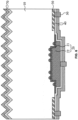
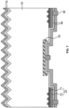
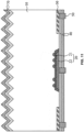
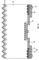
- the first embodiment of the disclosure provides a back contact structure of a solar cell. To facilitate explanation, merely the parts related to the embodiment of the disclosure are illustrated. With reference to FIG. 1 to FIG. 13 , the back contact structure of the solar cell provided by the embodiment of the disclosure comprises:
- the silicon substrate 10 has a front facing the sun and a back opposite to the front during a normal working period, and the front is an illuminated face; the back is disposed on the other side of the silicon substrate 10 with respect to the front, i.e., the front and the back are located on different sides, i.e., opposite sides, of the silicon substrate 10, where in this embodiment, the silicon substrate 10 is an N-type silicon slice, and it can be understood that, in other embodiments, the silicon substrate 10 may also be another silicon slice.
- the recesses are formed at intervals on the back surface of the silicon substrate 10; the recesses can be formed through laser ablation or through a combination of a mask (such as a hard mask, a silicon oxide mask, a silicon nitride mask, and a photoresist mask) and wet/dry etching; in this case, due to the recesses formed at intervals on the back surface of the silicon substrate 10, a region between two adjacent recesses located on the silicon substrate 10 is roughly in a protrusion shape, and thus a back pattern of the silicon substrate 10 generally appears to be formed by staggering the recesses and protrusions.
- a mask such as a hard mask, a silicon oxide mask, a silicon nitride mask, and a photoresist mask
- the first conductive regions 20 are disposed inside the recesses, and then the second conductive regions 30 are disposed outside the recesses; or as shown in FIG. 2 , the first conductive regions 20 are disposed outside the recesses, and then the second conductive regions 30 are disposed inside the recesses.
- the first doped region 22 and the second doped region have opposite conductivity types, where if the first doped region 22 is a P-type doped region, the second doped region is an N-type doped layer; or if the first doped region 22 is an N-type doped region, the second doped region is a P-type doped layer.
- the first dielectric layer 21 covers the first doped regions 22.
- the first conductive regions 20 are disposed inside the recesses, if the first dielectric layer 21 merely covers the first doped regions 22, as shown in FIG. 1 , the first dielectric layer 21 is connected to bottom walls and sidewalls of the recesses. If the first dielectric layer 21 further extends to cover the regions between the first doped regions 22 and the second doped regions, which is not part of the claimed invention, the connection state is shown in FIG. 3 .
- the connection state is shown in FIG. 2
- the connection state is shown in FIG. 4 .
- the first dielectric layer 21 is located between the silicon substrate 10 and the first doped regions 22, and is used as a tunneling structure; moreover, the first dielectric layer 21 and the first doped regions 22 connected thereto and covered thereby together form a passivated contact structure.
- the passivated contact structure provides good surface passivation for the back surface of the silicon substrate 10; in addition, generally speaking, the first dielectric layer 21 has a thin enough thickness, in which one type of current carriers achieves selective transmission through a tunneling principle, while another type of current carriers is hard to tunnel through the first dielectric layer 21 due to the existence of a barrier and a doped region field effect.
- the first dielectric layer 21 may allow one type of current carriers to tunnel through and enter the first doped regions 22 while blocking another type of current carriers from passing through to cause composition, so that interface composition can be obviously reduced, the solar cell has relatively high open-circuit voltage and short-circuit current, and then photovoltaic conversion efficiency is improved.
- a plurality of inner diffusion regions corresponding to the first doped regions 22 are formed on the surface of the silicon substrate 10 in contact with the first dielectric layer 21.
- the first conductive regions 20 are disposed inside the recesses; and in this case, the first dielectric layer 21 may be in contact with both bottom walls and sidewalls of the recesses, so that current carriers generated on the silicon substrate 10 would also be easily separated through the first dielectric layer 21 on the sidewalls of the recesses and selectively collected into the corresponding first doped regions 22, thereby facilitating multi-dimensional collection of the current carriers on the bottom walls and sidewalls of the recesses.
- the first dielectric layer 21 is preferably one of a tunneling oxide layer, an intrinsic silicon carbide layer and an intrinsic amorphous silicon layer, or a combination thereof.
- the first dielectric layer 21 may be a tunneling oxide layer of a single material, may also be a combination of a tunneling oxide layer and the intrinsic amorphous silicon layer of multiple materials, and may further be a combination of multiple layers of intrinsic amorphous silicon having different refractive indexes of a single material. It can be understood that the specific structural arrangement of the first dielectric layer 21 comprises, but not limited to, the several modes listed above, and according to actual usage needs, the first dielectric layer 21 is correspondingly configured, which is not specifically limited herein.
- the first dielectric layer 21 is preferably the tunneling oxide layer and the intrinsic silicon carbide layer; in this case, the tunneling oxide layer and the intrinsic silicon carbide layer are successively arranged outward from the silicon substrate 10, the tunneling oxide layer is in contact with the back surface of the silicon substrate 10, and the intrinsic silicon carbide layer is in contact with the first doped regions 22.
- the tunneling oxide layer preferably comprises one or more of a silicon oxide layer and an aluminum oxide layer.
- the first dielectric layer 21 may also be a combination of the silicon oxide layer and the aluminum oxide layer in the tunneling oxide layer.
- the intrinsic silicon carbide layer in the first dielectric layer 21 comprises an intrinsic hydrogenated silicon carbide layer.
- the tunneling oxide layer and the intrinsic silicon carbide layer reduce the density of interface states between the silicon substrate 10 and the first doped regions 22 as well as the second doped regions through chemical passivation.
- hydrogen in the intrinsic hydrogenated silicon carbide layer enters the silicon substrate 10 under the function of a diffusion mechanism and a thermal effect, to neutralize dangling bonds of the back surface of the silicon substrate 10, to passivate defects of the back surface of the silicon substrate 10, and to transfer an energy band in a forbidden band to a valence band or a conduction band to improve probability for the current carriers to enter the first doped regions 22 through the first dielectric layer 21.
- the first dielectric layer 21 preferably adopts the silicon oxide layer of 1-2 nm and the intrinsic silicon carbide layer of 2-5 nm; as compared with only using the silicon oxide layer as the tunneling structure, the intrinsic silicon carbide layer may further provide an additional hydrogen passivation effect; a preparing process window of the tunneling structure is enlarged, without influencing the tunneling effect; certainly, the silicon oxide layer of 1-2 nm, or the silicon oxide layer of 1 nm and the aluminum oxide layer of 1 nm, or two or more of the intrinsic silicon carbide layers having different refractive indexes can also be directly adopted; as can be understood, the specific structure arrangement of the first dielectric layer 21 comprises, but not limited to, the several specific examples listed above.
- the first dielectric layer 21 may also be an intrinsic microcrystalline silicon layer, an intrinsic microcrystalline silicon oxide layer, an intrinsic amorphous silicon oxide layer, etc. As shown in FIG. 1 to FIG. 13 , it is only shown that the first dielectric layer 21 is a one-layer structure; as can be understood, the specific structure of the first dielectric layer 21 is set according to actual needs and does not completely follow the accompanying drawings of the description.
- the first doped region 22 preferably comprises doped polycrystalline silicon or doped silicon carbide or doped amorphous silicon, where the doped silicon carbide may comprise doped hydrogenated silicon carbide, and the doped hydrogenated silicon carbide is specifically formed by adding hydrogen when depositing the silicon carbide.
- the first dielectric layer 21 comprises the silicon oxide layer and the intrinsic silicon carbide layer
- the first doped region 22 is specifically doped silicon carbide.
- the first doped region 22 may be doped polycrystalline silicon or the like.
- the first doped region 22 is specifically doped amorphous silicon.
- the first conductive region 20 comprising the first dielectric layer 21 and the first doped region 22 is disposed inside or outside the recess through deposition or the like.
- the thickness of the first dielectric layer 21 is 1-20 nm
- the thickness of the first conductive layer 20 is greater than 20 nm, i.e., the total thickness of the first dielectric layer 21 and the first doped region 22 is greater than 20 nm.
- the second conductive region 30 comprises the second doped region, and the second doped region is a doped layer.
- the doped layer is different from the first conductive region 20 which is grown inside the recess through deposition or the like, and the doped layer is a diffusion structure formed by doping different types of diffusion sources on the silicon substrate 10. Therefore, the doped layer is not grown. Instead, the silicon substrate 10 is partially diffused to form the doped layer.
- the second doped region has a junction depth of 0.01-1 ⁇ m, a sheet resistance of 10-500 ohm/sqr, and a surface concentration of 1 E18-1 E21 cm -3 .
- the second doped region may be a P-type doped layer or an N-type doped layer.
- the specific conductivity type of the first doped region 22 is set to be opposite to that of the second doped region.
- the P-type doped layer is formed by diffusion doped with boron, aluminum, gallium or the like
- the N-type doped layer is formed by diffusion doped with nitrogen, phosphorus, arsenic or the like.
- the N-type doped layer is an N + layer with respect to the silicon substrate 10 which is specifically an N-type silicon slice, i.e., the doped layer is formed by partial heavy doping.
- the distance between the first conductive regions 20 and the second conductive regions 30 is greater than 0 and less than or perennial to 500 ⁇ m, i.e., the first conductive regions 20 and the second conductive regions 30 may be adjacent to each other or spaced part from each other in a horizontal direction. That is to say, the first conductive regions 20 or the second conductive regions 30 disposed on the protrusions outside the recesses may be disposed on some or all regions of the protrusions.
- the first conductive regions 20 are disposed on the protrusions outside the recesses and the second conductive regions 30 are disposed inside the recesses, which is not part of the claimed invention, since the first conductive regions 20 are grown on the protrusions through deposition and the second conductive regions 30 disposed inside the recesses are formed by doping on the silicon substrate 10 on the bottoms of the recesses, the height difference between the recesses and the protrusions can achieve separation between the first conductive regions 20 and the second conductive regions 30.
- the first conductive regions 20 may be disposed on some or all regions of the protrusions, as shown in FIG. 2 , FIG. 4 , and FIG. 5 , which is configured according to actual usage needs.
- the second conductive regions 30 may be disposed on some regions of the protrusions, so as not to be connected to the first conductive regions 20 inside the recesses, as shown in FIG. 1 ; and when the second conductive regions 30 are disposed on all regions of the protrusions, the depth of each recess is greater than the thickness of the first conductive regions 20 and the junction depth of the second conductive region 30, so that the first conductive regions 20 and the second conductive regions 30 are not connected to each other.
- the depth of each recess is set to 0.01-10 ⁇ m. Therefore, when the first conductive region 20 is disposed inside the recess, there may be a case where the total thickness of the first conductive region 20 is less than or equal to the depth of the recess, i.e., the first conductive region 20 may be deposited merely inside the recess. In one embodiment of the disclosure, which is not part of the claimed invention, as shown in FIG.
- the first dielectric layer 21 when the second conductive regions 30 are disposed on some regions of the protrusions, the first dielectric layer 21 extends to cover regions between the first doped regions 22 and the second doped regions, and the thickness of the first conductive region 21 is greater than the depth of the recess, the first doped regions 22 may further extend to some regions of the protrusions and are not connected to the second doped regions.
- the first dielectric layer 21 and the first doped regions 22 disposed on the protrusion regions also form a passivated contact structure, and communicate with the first dielectric layer 21 and the first doped regions 22 in the recesses, thus increasing the contact area of the first dielectric layer 21 through which the current carriers selectively pass.
- the second conductive regions 30 are disposed inside the recesses, when the silicon substrate 10 inside the recesses is diffused at the diffusion source to form the second doped region, the sidewalls of the recess may also be correspondingly diffused to form the second doped region, so that the second doped region extends to part of regions between the recesses. Therefore, in one embodiment of the disclosure, the first doped regions 22 and/or the second doped regions may extend to part of the regions between the recesses.
- the first doped regions 22 extend out of the recesses to part of the regions between the recesses; or the second doped regions extend from the sidewalls of the recesses to part of the regions between the recesses; or the first doped regions 22 extend out of the recesses to part of the regions between the recesses, and at the same time, the second doped regions extend from the sidewalls of the recesses to part of the regions between the recesses.
- the width of the P-type doped region is 300-600 ⁇ m
- the width of the N-type doped region is 100-500 ⁇ m. That is, when the first conductive regions 20 are disposed inside the recesses, the width of the recess is as stated above; and when the first conductive regions 20 are disposed on the protrusions, the width of the protrusion is at least greater than the value stated above, so that the first conductive regions 20 are disposed on some or all regions of the protrusions.
- the width control requirement of dozens of microns for the set recess width is looser as compared with the existing trenches; it would be easier to prepare it as compared with preparing the existing trenches.
- the width of the P-type doped region is preferably set to 500 ⁇ m
- the width of the N-type doped region is preferably set to 300 ⁇ m
- the distance between the first conductive region 20 and the second conductive region 30 is preferably 100 ⁇ m.
- the second dielectric layer 40 covers regions between the first conductive regions 20 and the second conductive regions 30, or extends to cover the first conductive regions 20 and/or the second conductive regions 30. That is to say, as shown in FIG. 8 and FIG. 9 , the second dielectric layer 40 can merely cover the regions between the first doped regions 22 and the second doped regions; correspondingly, in this case, the conductive layer 50 covers the entire back of the first doped regions 22 and the first doped regions 22 for electrical connection. As shown in FIG. 1 and FIG. 2 , the second dielectric layer 40 may further extend to cover the first doped regions 22 and/or the second doped regions.
- the conductive layer 50 covers the remaining part of the back that does not cover the second dielectric layer 40 in the first doped regions 22 and the second doped regions, to form electrical connections to the first doped regions 22 and the second doped regions, respectively.
- the entire back of the back contact structure can also be completely covered, and in this case, when preparing the conductive layer 50, the conductive layer 50 penetrates through the second dielectric layer 40 by means of perforation or the like to form electrical connections to the first doped regions 22 and the second doped regions, respectively.
- the second dielectric layer 40 is preferably selected from one of an aluminum oxide layer, a silicon nitride layer, a silicon oxynitride layer, an intrinsic silicon carbide layer, an intrinsic amorphous silicon layer and a silicon oxide layer, or a combination thereof.
- the second dielectric layer 40 plays a passivation function and the second dielectric layer 40 is at least set as a one-layer structure; the refractive index of each layer is set to successively decrease outward from the silicon substrate 10, so that the film layer adjacent to the silicon substrate 10 plays a passivation function, while the film layer away from the silicon substrate 10 plays an anti-reflection function, to enhance the anti-reflection effect, thereby increasing the absorption and usage of light by the silicon substrate 10, to increase the short-circuit current density.
- the second dielectric layer 40 may further be a doped silicon layer (such as a doped microcrystalline silicon layer, a doped amorphous silicon layer, and a doped polycrystalline silicon layer), a doped silicon carbide layer (such as a doped polycrystalline silicon carbide layer), a doped silicon oxide layer (such as a doped polycrystalline silicon oxide and doped amorphous silicon oxide), etc.
- a doped silicon layer such as a doped microcrystalline silicon layer, a doped amorphous silicon layer, and a doped polycrystalline silicon layer
- a doped silicon carbide layer such as a doped polycrystalline silicon carbide layer
- a doped silicon oxide layer such as a doped polycrystalline silicon oxide and doped amorphous silicon oxide
- each film layer of a different structure in the second dielectric layer 40 may comprise a plurality of films with different refractive indexes, and according to the fact that the refractive index of each film layer is set to successively decrease outward from the silicon substrate 10, for example, the silicon oxide layer in the second dielectric layer 40 may comprise a plurality of silicon oxide film layers having the refractive index successively decreasing outward from the silicon substrate 10.
- the second dielectric layer 40 may be a three-layer structure comprising the silicon oxide layer/aluminum oxide layer, intrinsic silicon carbide layer, and silicon nitride layer/silicon oxynitride layer; in this case, the thickness of the silicon oxide layer/aluminum oxide layer located at a first layer at an inner side is greater than 0.5 nm, the thickness of the intrinsic silicon carbide layer located at a second layer is greater than 1 nm, and the thickness of the silicon nitride layer/silicon oxynitride layer located at a third layer at an outer side is greater than 50 nm.
- the second dielectric layer 40 may further be a two-layer structure comprising the aluminum oxide layer, and silicon nitride layer/silicon oxynitride layer; in this case, the thickness of the aluminum oxide layer located at a first layer at an inner side is greater than 1 nm, and the thickness of the silicon nitride layer/silicon oxynitride layer located at a second layer at an outer side is greater than 50 nm.
- the second dielectric layer 40 may further be a three-layer structure comprising the silicon oxide layer/aluminum oxide layer, doped polycrystalline silicon layer/doped polycrystalline silicon carbide layer/doped polycrystalline silicon oxide layer, and silicon nitride layer/silicon oxynitride layer; in this case, the thickness of the silicon oxide layer/aluminum oxide layer located at a first layer at an inner side is 0.5-3 nm, the thickness of the doped polycrystalline silicon layer/doped polycrystalline silicon carbide layer/doped polycrystalline silicon oxide layer located at a second layer is 20-100 nm, and the thickness of the silicon nitride layer/silicon oxynitride layer located at a third layer at an outer side is greater than 50 nm.
- the second dielectric layer 40 may further be a three-layer structure comprising the intrinsic amorphous silicon layer, doped amorphous silicon layer/doped amorphous silicon oxide layer, and silicon nitride layer/silicon oxynitride layer; in this case, the thickness of the intrinsic amorphous silicon layer located at a first layer at an inner side is 2-10 nm, the thickness of the doped amorphous silicon layer/doped amorphous silicon oxide layer located at a second layer is 2-50 nm, and the thickness of the silicon nitride layer/silicon oxynitride layer located at a second layer at an outer side is greater than 50 nm.
- the second dielectric layer 40 may further be a three-layer structure comprising the silicon oxide/aluminum oxide layer, intrinsic silicon carbide layer/doped amorphous silicon oxide layer, and silicon nitride layer/silicon oxynitride layer; in this case, the thickness of the silicon oxide/aluminum oxide layer located at a first layer at an inner side is 0.5-3 nm, the thickness of the intrinsic silicon carbide layer/doped amorphous silicon oxide layer located at a second layer is 10-50 nm, and the thickness of the silicon nitride layer/silicon oxynitride layer located at a second layer at an outer side is greater than 50 nm.
- the specific structure arrangement of the second dielectric layer 40 comprises, but not limited to, several specific examples listed above.
- the second dielectric layer 40 is preferably a two-layer structure of an aluminum oxide layer and an intrinsic silicon carbide layer or a two-layer structure of a silicon oxide layer and an intrinsic silicon carbide layer, and in this case, the overall thickness of the second dielectric layer 40 is greater than 25 nm, where it is normally 70-80 nm during normal production and preparation.
- the intrinsic silicon carbide layer not only provides a hydrogen passivation effect, but also reduces parasitic light absorption due to a large optical band gap and a small absorption coefficient with respect to the intrinsic amorphous silicon layer and the doped polycrystalline silicon layer or the like. Furthermore, the thickness of the aluminum oxide layer or the silicon oxide layer in the second dielectric layer 40 is less than 25 nm, and the thickness of the intrinsic silicon carbide layer in the second dielectric layer 40 is greater than 10 nm. In the multi-layer structure indicated in the embodiment of the disclosure, the order thereof is to arrange outward from the silicon substrate 10.
- the second dielectric layer 40 above comprises the aluminum oxide layer and intrinsic silicon carbide layer
- the aluminum oxide layer is close to the silicon substrate 10
- the intrinsic silicon carbide layer is close to the outer side.
- the second dielectric layer 40 is a two-layer structure; as can be understood, the second dielectric layer 40 may further be other layer number, and the specific structure thereof is set according to actual needs and is not completely as shown in the accompanying drawings of the description.
- each of the accompanying drawings of the description is merely used for describing each specific structure distribution in the back contact structure thereof, but it does not correspond to the actual size dimension of each structure.
- the thickness of the first dielectric layer 21 above is 1-20 nm, and the thickness of the second dielectric layer 40 is greater than 25 nm; in the accompanying drawings, they do not completely correspond to the specific actual size dimensions in this embodiment, and should depend on the specific parameters provided in this embodiment.
- the intrinsic silicon carbide layer in the second dielectric layer 40 comprises at least one first intrinsic silicon carbide film having a different refractive index.
- the refractive index of each first intrinsic silicon carbide film successively decreases outward from the back surface of the silicon substrate 10.
- the refractive index of each material is generally selected as: the refractive index of monocrystalline silicon is 3.88; the refractive index of amorphous silicon is 3.5-4.2; the refractive index of polycrystalline silicon is 3.93; the refractive index of silicon carbide is 2-3.88; the refractive index of silicon nitride is 1.9-3.88; the refractive index of silicon oxynitride is 1.45-3.88; the refractive index of silicon oxide is 1.45; and the refractive index of aluminum oxide is 1.63.
- the refractive index of each material above may further be set as others according to actual usage needs, and is not specifically limited herein.
- a magnesium fluoride layer is disposed at an outer layer of the second dielectric layer 40, i.e., based on the one of an aluminum oxide layer, a silicon nitride layer, a silicon oxynitride layer, an intrinsic silicon carbide layer, an intrinsic amorphous silicon layer and a silicon oxide layer, or a combination thereof selected by the second dielectric layer 40, the magnesium fluoride layer can further be disposed at the outer layer of the second dielectric layer 40.
- the refractive index requirement for the magnesium fluoride layer is the lowest, and generally, the refractive index thereof is set as 1.4, for enhancing the optical function of anti-reflection.
- the conductive layer 50 is a TCO transparent conductive film and/or a metal electrode.
- the metal electrode comprises a silver electrode, a copper electrode, an aluminum electrode, a tin-clad copper electrode, or a silver-clad copper electrode.
- the copper electrode is electro-plated copper prepared through an electroplating process or a copper electrode prepared through physical vapor deposition.
- the electro-plated copper uses nickel, chromium, titanium, and tungsten electrodes as a seed layer or a protection layer thereof
- the recess is an arc, a trapezoid, or a square. As shown in FIG. 1 and FIG. 2 , in a specific embodiment, the recess is a square. As shown in FIG. 10 , in another specific embodiment, the recess where the first conductive region 20 is disposed is an arc. As shown in FIG. 11 , in another specific embodiment, the recess where the first conductive region 20 is disposed is a trapezoid. It can be understood that the second conductive region 30 can also be disposed inside the arc-shaped recess or the trapezoidal recess.
- the recess is preferably to be set as an arc or a trapezoid, because when the recess is set as an arc or a trapezoid, an effect of reflecting light by the inner wall of the recess is better, and the surface area of the first dielectric layer 21 specifically as the tunneling structure in contact with the silicon substrate 10 can further be increased when the first conductive regions 20 are disposed inside the recesses.
- the recess is set as a square, the actual production process is simpler. Therefore, the shape of the recess is correspondingly set according to actual usage needs, which is not specifically limited herein.
- the first dielectric layer 21 is connected to the bottom walls of the recesses and the second dielectric layer 40 is further connected to the sidewalls of the recesses when the first conductive regions 20 are disposed inside the recesses.
- the recess region is covered using the mask, and then when the mask is removed in a subsequent process, silicon in part of the silicon substrate 10 near the first doped region 22 will be corroded to widen the recess; and when the second dielectric layer 40 is deposited in a subsequent process, the second dielectric layer 40 will be deposited in a blank region, so that the second dielectric layer 40 is connected to the sidewall of the recess.
- an arc-shaped recess (such as an ellipsoid-shaped recess)
- the first dielectric layer 21 and the first doped region 22 cannot be deposited onto the inner wall of the arc-shaped recess in the long-axis direction, and thus the blank region may be filled with the second dielectric layer 40 during deposition thereof so that the second dielectric layer 40 is connected to the sidewall of the arc-shaped recess, or there may be another case where the second dielectric layer 40 cannot be deposited to the blank region during deposition so that a certain gap is formed between the sidewall of the arc-shaped recess and the first dielectric layer 21 and the first doped region 22.
- the first dielectric layer 21 is directly connected to the sidewall of the recess, so that the first dielectric layer 21 disposed on the sidewall of the recess can allow selective pass-through of the current carriers to achieve multi-dimension collection.
- the back surface of the silicon substrate 10 located on regions between the first conductive regions 20 and the second conductive regions 30 comprises a rough texture structure 60.
- the rough texture structure 60 is generally made through texturing, comprising forming hemispherical textures through acid texturing and forming pyramid-shaped textures through alkaline texturing, or forming pyramid-shaped textures through alkaline texturing and then performing rounding treatment on pyramid apexes through acid texturing.
- the second embodiment of the disclosure provides a selective contact region buried solar cell.
- the selective contact region buried solar cell provided by the embodiment of the disclosure comprises:
- the second dielectric layer 40 and the third dielectric layer 70 may be respectively prepared on the front and back surface of the silicon substrate 10 through the same process.
- the third dielectric layer 70 may have the same structure as the second dielectric layer 40 in the foregoing embodiment. Therefore, with reference to the foregoing embodiment, preferably, the third dielectric layer 70 may also be selected from one of an aluminum oxide layer, a silicon nitride layer, a silicon oxynitride layer, a silicon carbide layer, an intrinsic amorphous silicon layer and a silicon oxide layer, or a combination thereof.
- the third dielectric layer 70 may further have a three-layer structure comprising the silicon oxide layer/aluminum oxide layer and the doped polycrystalline silicon layer/doped polycrystalline silicon carbide layer/doped polycrystalline silicon oxide layer and the silicon nitride layer/silicon oxynitride layer, or a three-layer structure comprising the intrinsic amorphous silicon layer and the doped amorphous silicon layer/doped amorphous silicon oxide layer and the silicon nitride layer/silicon oxynitride layer, or a three-layer structure comprising the silicon oxide layer/aluminum oxide layer and the intrinsic silicon carbide layer/doped amorphous silicon oxide layer and the silicon nitride layer/silicon oxynitride layer.
- the third dielectric layer 70 also correspondingly has a two-layer structure comprising the silicon oxide layer and the silicon carbide layer, or a two-layer structure comprising the aluminum oxide layer and the silicon carbide layer, and the thickness of the third dielectric layer 70 is greater than 50 nm.
- the thickness of the aluminum oxide layer or the silicon oxide layer in the third dielectric layer 70 is less than 40 nm, and the thickness of the silicon carbide layer in the third dielectric layer 70 is greater than 10 nm.
- the silicon carbide layer not only provides a hydrogen passivation effect, but also reduces parasitic light absorption due to a large optical band gap and a small absorption coefficient with respect to the intrinsic amorphous silicon layer and the doped polycrystalline silicon layer or the like.
- the silicon carbide layer in the third dielectric layer 70 comprises at least one silicon carbide film having a different refractive index. The refractive index of each silicon carbide film successively decreases outward from the front surface of the silicon substrate 10.
- a magnesium fluoride layer is disposed at an outer layer of the third dielectric layer 70. The refractive index requirement for the magnesium fluoride layer at the outermost layer is the lowest, and generally, the refractive index is set as 1.4, for enhancing the optical function of anti-reflection.
- the third dielectric layer 70 may have a structural arrangement different from the second dielectric layer 40 in the foregoing embodiment, and the film structures of the second dielectric layer 40 and the third dielectric layer 70 are correspondingly set according to actual usage needs, which is not specifically limited herein.
- an electric field layer or a floating junction is further disposed between the front surface of the silicon substrate 10 and the third dielectric layer 70, specifically comprising performing phosphorus diffusion on the silicon substrate 10 to obtain the electric field layer or performing boron diffusion to obtain the floating junction.
- the electric field layer or the floating junction serves as a Front-Surface Field (FSF) of the selective contact region buried solar cell.
- recesses are disposed at intervals on a back surface of a silicon substrate, and first conductive regions are disposed inside or outside the recesses and the second conductive regions are disposed outside or inside the recesses in an alternate manner, so that separation between the first conductive regions and the second conductive regions is implemented through some recesses or some protrusions outside the recesses; moreover, the recesses disposed have a lower width control requirement than existing trenches, and preparation of the recesses is easier than preparation of the existing trenches.
- the arrangement of the recesses enables the first dielectric layer to be in contact with both bottom walls and sidewalls of the recesses when the first conductive regions are disposed inside the recesses, current carriers generated on the silicon substrate would also be easily separated through the first dielectric layer on the sidewalls of the recesses and selectively collected into the corresponding first doped regions, so that leakage current can be reduced and selective transport of the current carriers in longitudinal and transverse directions can also be implemented, thereby facilitating multi-dimensional collection of the current carriers on the bottom walls and sidewalls of the recesses.
- a second dielectric layer disposed is at least one in number, multi-layer passivation is achieved on the back surface of the silicon substrate through the second dielectric layer having at least one layer, and then a better passivation effect is yielded and inner back reflection is enhanced, thereby yielding a better passivation effect and a better inner back reflection effect and solving the existing problems of a high trench width control requirement and a poor passivation effect.
- the third embodiment of the disclosure provides a selective contact region buried solar cell manufacturing method. To facilitate explanation, merely the parts related to the embodiment of the disclosure are illustrated. With reference to FIG. 14 , the selective contact region buried solar cell manufacturing method provided by the embodiment of the disclosure is used for preparing the selective contact region buried solar cell as stated in the preceding embodiment, and specifically, the method comprises the following steps.
- a plurality of recesses is formed at intervals on a back surface of a silicon substrate.
- the method further comprises pre-treating the silicon substrate.
- the pre-treatment above comprises cleaning the silicon substrate and removing a damaged layer.
- the pre-treatment comprises:
- the recesses may be formed in the following ways: way I: the part where the recesses need to be disposed at intervals is directly slotted through laser and partial silicon crystal is removed from the back surface of the silicon substrate, to form the desired recesses; way II: the silicon substrate is subjected to thermal oxidation treatment so that a silicon oxide layer is formed on the entire surface of the silicon substrate, silicon oxide in part of the regions on the front and back surface of the silicon substrate is removed through laser slotting, and then silicon oxide is removed using an acid (such as HF) through wet etching, to form the desired recesses; way III: a silicon nitride layer is deposited on the back surface of the silicon substrate through PECVD, silicon nitride in part of the region on the back is removed through laser slotting, and then silicon nitride is removed through wet etching, to form the desired recesses; way IV, silicon nitride is deposited on the back surface of the silicon substrate or the silicon
- way II is preferably used for forming the recesses, where in way II, the thermal oxidation treatment step specifically comprises: performing dry-oxygen oxidation/steam oxidation/wet-oxygen oxidation (i.e., dry-oxygen + steam) in a quartz tube, where specific reactants comprise oxygen and/or high-purity steam, the reaction pressure is 50-1000 mbar, the reaction temperature is 900-1200°C, and the thickness of silicon oxide prepared from the reaction is greater than 10 nm.
- dry-oxygen oxidation/steam oxidation/wet-oxygen oxidation i.e., dry-oxygen + steam
- specific reactants comprise oxygen and/or high-purity steam
- the reaction pressure is 50-1000 mbar
- the reaction temperature is 900-1200°C
- the thickness of silicon oxide prepared from the reaction is greater than 10 nm.
- the step of removing silicon oxide through laser slotting specifically comprises: removing silicon oxide to be removed through slotting by laser having a laser wavelength of 532 nm, a laser power of 10-60 W, a laser frequency less than or equal to 250-1500 KHz, and a laser pulse width of 3-50 ns.
- An alkaline solution and isopropyl acetone are used in the wet etching step, where the alkaline solution is KOH or TMAH, the concentration of the alkaline solution is 1-5%, the content of isopropyl acetone is 1-10%, the reaction temperature is 60-85°C, and the reaction time is 10-30 min.
- An acidic solution in the step of removing silicon oxide using the acid is HF, where the concentration of the acidic solution is 1-5%, the reaction temperature is room temperature, and the reaction time is 3-10 min.
- the depth of the formed recess is 0.01-10 ⁇ m.
- the formed recess may be an arc, a trapezoid, or a square. Since trenches used in the related art are prepared by laser perforation or wet etching, the width control requirement for the trenches is high and it is difficult to prepare. However, preparation of the recesses in this embodiment is easier than preparation of existing trenches, and does not have a strict width control requirement as the existing trenches.
- first conductive regions and second conductive regions are prepared alternately on the silicon substrate, where one of the first conductive region and the second conductive region is disposed inside the recess and the other one is disposed outside the recess, each first conductive region comprises a first dielectric layer and a first doped region which are disposed successively, and each second conductive region comprises a second doped region;
- the specific production process may further comprise texturing the front surface of the silicon substrate.
- texturing on the front is mainly achieved by corrosion using an alkaline solution, where the alkaline solution reacts with the silicon substrate to generate a water-soluble compound, and a pyramid-shaped textured structure is formed on the surface.
- the front and back surface of the silicon substrate can be textured at the same time; and when the back surface of the silicon substrate does not need to have a rough texture structure, a silicon nitride protection layer is deposited on the back surface of the silicon substrate, the front is then textured, and the silicon nitride protection layer is removed from the back through laser, thereby avoiding texturing on the back surface of the silicon substrate.
- the alternately preparing first conductive regions and second conductive regions on the silicon substrate is implemented in the following steps:
- the first conductive regions and the second conductive regions are respectively disposed at different positions inside and outside the recesses, where specifically, when the first conductive region comprising the first dielectric layer and the first doped region is disposed inside the recess, the second conductive region comprising the second doped region is disposed outside the recess; and correspondingly, when the first dielectric layer and the first doped region are disposed outside the recess, the second doped region is disposed inside the recess.
- first doped region and the second doped region have opposite conductivity types, where if the first doped region is a P-type doped region, the second doped region is correspondingly an N-type doped layer; or if the first doped region is an N-type doped region, the second doped region is correspondingly a P-type doped layer.
- the first conductive regions are prepared before the preparation of the second conductive regions, or the second conductive regions are prepared before the preparation of the first conductive regions. Accordingly, the order of preparing the first conductive regions and the second conductive regions is set in consideration of the convenience of an actual technological process, which is not specifically limited herein.
- the first conductive regions are prepared inside or outside the recesses, and then the second conductive regions are prepared outside or inside the corresponding recesses.
- the successively preparing the first dielectric layer and the first doped region having a first conductivity type inside or outside the recess specifically refers to preparing the first dielectric layer inside or outside the recess and then performing in-situ deposition or ex-situ deposition on the first dielectric layer to prepare the first doped region having the first conductivity type.
- the first dielectric layer is prepared according to a high-temperature oxidation process, a deposition process or the like, which is set depending on the type of the first dielectric layer to be specifically deposited and is not specifically limited therein.
- the first dielectric layer is one of a tunneling oxide layer, an intrinsic silicon carbide layer and an intrinsic amorphous silicon layer, or a combination thereof, and the thickness of the first dielectric layer is 1-20 nm.
- the step of preparing the first doped region on the first dielectric layer comprises:
- the first conductive regions are disposed inside/outside the recesses and the first doped region in the first conductive region is the P-type doped region
- the protrusions outside the recess/the recesses in which deposition is not needed are shielded with a mask method.
- in-situ deposition of P-type amorphous silicon/P-type amorphous silicon carbide is performed inside/outside the recesses, and then the temperature is increased to 700-1000°C directly using a high-temperature or laser heating method.
- the P-type amorphous silicon/P-type amorphous silicon carbide inside/outside the recesses is changed into P-type polycrystalline silicon/P-type silicon carbide, to obtain the P-type doped region, i.e., the first doped region having the first conductivity type.
- the mask may be a hard mask, a silicon nitride mask, a silicon oxide mask, and a photoresist mask.
- the step of preparing the first doped region on the first dielectric layer comprises:
- the step of performing the first conductivity type of doping on the intrinsic amorphous silicon or the intrinsic silicon carbide specifically comprises:
- intrinsic amorphous silicon or intrinsic silicon carbide is deposited on the first dielectric layer; then the first conductivity type of ions are injected onto the intrinsic amorphous silicon or intrinsic silicon carbide for doping (when the first doped region is the P-type doped region, P-type ions containing elements boron, aluminum, gallium or the like are injected, and when the first doped region is the N-type doped region, N-type ions containing elements nitrogen, phosphorus, arsenic or the like are injected), or the first conductivity type of doping source is deposited, with a mask method, onto the intrinsic amorphous silicon or intrinsic silicon carbide for doping (when the first doped region is the P-type doped region, a P-type doping source containing boron, aluminum, gallium or the like (such as borosilicate glass) is deposited for doping to form P-type amorphous silicon/P-type silicon carbide, and when the first doped region is the N-
- deposition may be performed on the sides and front surface of the silicon substrate, after high-temperature crystallization, it is required to add wet etching treatment to achieve bypass plating.
- the first conductivity type of doping source is deposited for doping and after high-temperature crystallization treatment is completed, it is also required to remove the doping source through laser or the like.
- the step of preparing the first doped region on the first dielectric layer further comprises:
- the thin first dielectric layer may be partially broken.
- attachment may occur at the broken part of the first dielectric layer and the back surface of the silicon substrate, and then a plurality of inner diffusion regions corresponding to the first doped regions are formed on the surface of the silicon substrate in contact with the first dielectric layer.
- the step of preparing the second doped region having a second conductivity type outside or inside the corresponding recess comprises:
- the specific preparation process comprises: way I: introducing a source gas containing elements boron, aluminum, gallium or the like (such as a borane gas or a carrier gas carrying boron trichloride or boron tribromide) for thermal diffusion to form the P-type doped layer; way II: depositing a doping source containing boron, aluminum, gallium or the like (such as borosilicate glass) for thermal diffusion to form the P-type doped layer; way III: preparing an aluminum electrode above the doped layer and forming the P-type doped layer doped with aluminum in a high-temperature process; way IV: spin-coating a doping source containing boron, aluminum, gallium or the like (such as boron tribromide) for thermal diffusion to form the P-type doped layer; and way V: injecting ions containing elements boron, aluminum, gallium or the like and performing high-temperature diffusion to form the P
- the specific preparation process comprises: way I: introducing a source gas containing elements such as nitrogen, phosphorus, arsenic or the like (such as a phosphorane gas or a carrier gas carrying phosphorus oxychloride) for thermal diffusion to form the N-type doped layer; way II: depositing a doping source containing nitrogen, phosphorus, arsenic or the like (such as phosphosilicate glass) for thermal diffusion to form the N-type doped layer; way III: spin-coating a doping source containing nitrogen, phosphorus, arsenic or the like (such as phosphorus oxychloride) for thermal diffusion to form the N-type doped layer; and way IV: injecting ions containing elements such as nitrogen, phosphorus, arsenic or the like and performing high-temperature diffusion to form the N-type doped layer. After a doping source is deposited for thermal diffusion, it is also required to remove the doping source through laser or
- a second dielectric layer and a third dielectric layer are respectively prepared on the back and front surface of the silicon substrate.
- the method may further comprise: texturing the positions between the first conductive regions and the second conductive regions on the back surface of the silicon substrate to obtain the rough texture structure.
- the specific texturing process may refer to the preceding text.
- the preparation is implemented depending on the specific composition types of the second dielectric layer and the third dielectric layer, which is not specifically limited therein.
- the second dielectric layer and the third dielectric layer may be one of an aluminum oxide layer, a silicon nitride layer, a silicon oxynitride layer, an intrinsic silicon carbide layer, an intrinsic amorphous silicon layer and a silicon oxide layer, or a combination thereof.
- the refractive index of each layer is set to successively decrease outward from the silicon substrate, and a magnesium fluoride layer having the lowest requirement for the refractive index may be prepared at the outermost layer.
- an electric field layer or a floating junction may be prepared first, specifically comprising performing phosphorus diffusion on the silicon substrate to obtain the electric field layer or performing boron diffusion to obtain the floating junction.
- the electric field layer or the floating junction serves as the FSF of the selective contact region buried solar cell.
- a conductive layer is prepared on the first conductive regions and the second conductive regions.
- the conductive layer when the second dielectric layer only covers regions between the first doped regions and the second doped regions in the silicon substrate, the conductive layer covers the entire back of the first doped regions and the second doped regions for electrical connection; when the second dielectric layer extends to cover the first doped regions and the second doped regions, the conductive layer covers the back of the remaining part that does not cover the second dielectric layer in the first doped regions and the second doped regions; and when the second dielectric layer covers the entire back surface of the silicon substrate, the conductive layer passes through the second dielectric layer as well as the first doped regions and the second doped regions through perforation or the like for electrical connection, so that first electrodes are formed on the first doped regions and second electrodes are formed on the second doped regions.
- the fourth embodiment of the disclosure further provides a cell assembly comprising the selective contact region buried solar cell according to the preceding embodiment.
- recesses are disposed at intervals on a back surface of a silicon substrate, and first conductive regions are disposed inside or outside the recesses and the second conductive regions are disposed outside or inside the recesses in an alternate manner, so that separation between the first conductive regions and the second conductive regions is implemented through some recesses or some protrusions outside the recesses; moreover, the recesses disposed have a lower width control requirement than existing trenches, and preparation of the recesses is easier than preparation of the existing trenches.
- the arrangement of the recesses enables the first dielectric layer to be in contact with both bottom walls and sidewalls of the recesses when the first conductive regions are disposed inside the recesses, current carriers generated on the silicon substrate would also be easily separated through the first dielectric layer on the sidewalls of the recesses and selectively collected into the corresponding first doped regions, so that leakage current can be reduced and selective transport of the current carriers in longitudinal and transverse directions can also be implemented, thereby facilitating multi-dimensional collection of the current carriers on the bottom walls and sidewalls of the recesses.
- a second dielectric layer disposed is at least one in number, multi-layer passivation is achieved on the back surface of the silicon substrate through the second dielectric layer having at least one layer, and then a better passivation effect is yielded and inner back reflection is enhanced, thereby yielding a better passivation effect and a better inner back reflection effect and solving the existing problems of a high trench width control requirement and a poor passivation effect.
- the fifth embodiment of the disclosure further provides a photovoltaic system comprising the cell assembly according to the preceding embodiments.
- recesses are disposed at intervals on a back surface of a silicon substrate, and first conductive regions are disposed inside or outside the recesses and the second conductive regions are disposed outside or inside the recesses in an alternate manner, so that separation between the first conductive regions and the second conductive regions is implemented through some recesses or some protrusions outside the recesses; moreover, the recesses disposed have a lower width control requirement than existing trenches, and preparation of the recesses is easier than preparation of the existing trenches.
- the arrangement of the recesses enables the first dielectric layer to be in contact with both bottom walls and sidewalls of the recesses when the first conductive regions are disposed inside the recesses, current carriers generated on the silicon substrate would also be easily separated through the first dielectric layer on the sidewalls of the recesses and selectively collected into the corresponding first doped regions, so that leakage current can be reduced and selective transport of the current carriers in longitudinal and transverse directions can also be implemented, thereby facilitating multi-dimensional collection of the current carriers on the bottom walls and sidewalls of the recesses.
- a second dielectric layer disposed is at least one in number, multi-layer passivation is achieved on the back surface of the silicon substrate through the second dielectric layer having at least one layer, and then a better passivation effect is yielded and inner back reflection is enhanced, thereby yielding a better passivation effect and a better inner back reflection effect and solving the existing problems of a high trench width control requirement and a poor passivation effect.
Landscapes
- Engineering & Computer Science (AREA)
- Computer Hardware Design (AREA)
- Microelectronics & Electronic Packaging (AREA)
- Power Engineering (AREA)
- Physics & Mathematics (AREA)
- Condensed Matter Physics & Semiconductors (AREA)
- Electromagnetism (AREA)
- General Physics & Mathematics (AREA)
- Life Sciences & Earth Sciences (AREA)
- Sustainable Development (AREA)
- Sustainable Energy (AREA)
- Chemical & Material Sciences (AREA)
- Crystallography & Structural Chemistry (AREA)
- Manufacturing & Machinery (AREA)
- Inorganic Chemistry (AREA)
- Photovoltaic Devices (AREA)
Claims (23)
- Rückkontaktstruktur für eine Solarzelle, wobei die Rückkontaktstruktur umfasst:ein Siliziumsubstrat (10), wobei das Siliziumsubstrat (10) eine Rückfläche umfasst, die eine Vielzahl von in Intervallen angeordneten Vertiefungen umfasst;eine Vielzahl von ersten leitfähigen Bereichen (20) und eine Vielzahl von zweiten leitfähigen Bereichen (30), die abwechselnd auf der Rückfläche des Siliziumsubstrats (10) angeordnet sind; wobei jeder erste leitfähige Bereich (20) eine erste dielektrische Schicht (21) und einen ersten dotierten Bereich (22) umfasst, die nacheinander angeordnet sind, und jeder zweite leitfähige Bereich (30) einen zweiten dotierten Bereich umfasst;eine zweite dielektrische Schicht (40), die zwischen der Vielzahl von ersten leitfähigen Bereichen (20) und der Vielzahl von zweiten leitfähigen Bereichen (30) angeordnet ist, wobei die zweite dielektrische Schicht (40) mindestens eine an der Zahl ist; undeine leitfähige Schicht (50), die auf der Vielzahl von ersten leitfähigen Bereichen (20) und der Vielzahl von zweiten leitfähigen Bereichen (30) angeordnet ist;wobei:der erste dotierte Bereich (22) ein P-dotierter Bereich ist und der zweite dotierte Bereich eine N-dotierte Schicht ist; oder der erste dotierte Bereich (22) ein N-dotierter Bereich ist und der zweite dotierte Bereich eine P-dotierte Schicht ist;der erste dotierte Bereich (22) dotiertes polykristallines Silizium umfasst; unddie erste dielektrische Schicht (21) eine Tunneloxidschicht umfasst;wobeidie Vielzahl von ersten leitfähigen Bereichen (20) jeweils innerhalb der Vielzahl von Vertiefungen angeordnet sind und die Vielzahl von zweiten leitfähigen Bereichen (30) außerhalb der Vielzahl von Vertiefungen angeordnet sind;dadurch gekennzeichnet, dasseine Tiefe der Vielzahl von Vertiefungen größer ist als eine Dicke jedes ersten leitfähigen Bereichs (20), wodurch jeder erste leitfähige Bereich (20) und sowohl die erste dielektrische Schicht (21) als auch die erste dotierte Schicht (22) innerhalb jeder Vertiefung eingeschlossen sind, und die zweiten leitfähigen Bereiche (30) nur auf Teilen der Bereiche außerhalb der Vertiefungen angeordnet sind, derart, dass die ersten leitfähigen Bereiche (20) und die zweiten leitfähigen Bereiche (30) in einer horizontalen Richtung durch Abschnitte des Siliziumsubstrats (10) und der zweiten dielektrischen Schicht (40) über den Abschnitten des Siliziumsubstrats (10) voneinander beabstandet sind.
- Rückkontaktstruktur nach Anspruch 1, wobei die zweite dielektrische Schicht (40) eine Aluminiumoxidschicht, eine Siliziumnitridschicht, eine Siliziumoxynitridschicht, eine intrinsische Siliziumkarbidschicht, eine intrinsische amorphe Siliziumschicht, eine Siliziumoxidschicht, oder eine Kombination davon umfasst.
- Rückkontaktstruktur nach Anspruch 1, wobei ein Teil der Rückfläche des Siliziumsubstrats (10) zwischen der Vielzahl von ersten leitfähigen Bereichen (20) und der Vielzahl von zweiten leitfähigen Bereichen (30) eine Struktur mit rauer Textur (60) umfasst.
- Rückkontaktstruktur nach Anspruch 1, wobei eine Breite des P-dotierten Bereichs 300-600 µm beträgt, und eine Breite des N-dotierten Bereichs 100-500 µm beträgt.
- Rückkontaktstruktur nach Anspruch 1, wobei die Vielzahl von Vertiefungen in Form eines Bogens, eines Trapezes oder eines Quadrats vorliegen.
- Rückkontaktstruktur nach Anspruch 1, wobei der zweite dotierte Bereich eine Übergangstiefe von 0,01-1 um, einen Schichtwiderstand von 10-500 Ohm/Quadrat und eine Flächenkonzentration von 1E18-1E21 cm-3 aufweist.
- Rückkontaktstruktur nach Anspruch 1, wobei eine Dicke der ersten dielektrischen Schicht (21) 1-20 nm beträgt, und eine Gesamtdicke der Vielzahl von ersten leitfähigen Bereichen (20) größer als 20 nm ist.
- Rückkontaktstruktur nach Anspruch 1, wobei die Tunneloxidschicht eine oder mehrere von einer Siliziumoxidschicht und einer Aluminiumoxidschicht umfasst.
- Rückkontaktstruktur nach Anspruch 2, wobei die zweite dielektrische Schicht (40) eine Kombination der Aluminiumoxidschicht und der intrinsischen Siliziumkarbidschicht umfasst, oder die zweite dielektrische Schicht (40) eine Kombination der Siliziumoxidschicht und der intrinsischen Siliziumkarbidschicht umfasst, und eine Dicke der zweiten dielektrischen Schicht (40) größer als 25 nm ist.
- Rückkontaktstruktur nach Anspruch 9, wobei eine Dicke der Aluminiumoxidschicht oder der Siliziumoxidschicht in der zweiten dielektrischen Schicht (40) kleiner als 25 nm ist, und eine Dicke der intrinsischen Siliziumkarbidschicht in der zweiten dielektrischen Schicht (40) größer als 10 nm ist.
- Rückkontaktstruktur nach Anspruch 1, wobei eine Magnesiumfluoridschicht an einer Außenschicht der zweiten dielektrischen Schicht (40) angeordnet ist.
- Rückkontaktstruktur nach Anspruch 1, wobei die leitfähige Schicht (50) ein transparentes leitfähiges Oxid (TCO) und/oder eine Metallelektrode ist.
- Rückkontaktstruktur nach Anspruch 12, wobei die Metallelektrode eine Silberelektrode, eine Kupferelektrode, eine Aluminiumelektrode, eine verzinnte Kupferelektrode oder eine versilberte Kupferelektrode umfasst.
- Rückkontaktstruktur nach Anspruch 13, wobei die Kupferelektrode elektroplattiertes Kupfer ist, das durch einen Elektroplattierungsprozess hergestellt wird, oder eine Kupferelektrode, die durch physikalische Dampfabscheidung hergestellt wird.
- Vergrabene Solarzelle mit selektiven Kontaktbereichen, umfassend:die Rückkontaktstruktur nach einem der Ansprüche 1 bis 14; undeine dritte dielektrische Schicht (70), die auf einer Vorderfläche des Siliziumsubstrats (10) angeordnet ist.
- Vergrabene Solarzelle mit selektiven Kontaktbereichen nach Anspruch 15, wobei die dritte dielektrische Schicht (70) eine von einer Aluminiumoxidschicht, einer Siliziumnitridschicht, einer Siliziumoxynitridschicht, einer Siliziumkarbidschicht, einer intrinsischen amorphen Siliziumschicht und einer Siliziumoxidschicht, oder eine Kombination davon ist.
- Vergrabene Solarzelle mit selektiven Kontaktbereichen nach Anspruch 16, wobei die dritte dielektrische Schicht (70) eine Kombination der Siliziumoxidschicht und der Siliziumkarbidschicht ist, oder die dritte dielektrische Schicht (70) eine Kombination der Aluminiumoxidschicht und der Siliziumkarbidschicht umfasst, und eine Dicke der dritten dielektrischen Schicht (70) größer als 50 nm ist.
- Vergrabene Solarzelle mit selektiven Kontaktbereichen nach Anspruch 17, wobei eine Dicke der Aluminiumoxidschicht oder der Siliziumoxidschicht in der dritten dielektrischen Schicht (70) kleiner als 40 nm ist, und eine Dicke der Siliziumkarbidschicht in der dritten dielektrischen Schicht (70) größer als 10 nm ist.
- Vergrabene Solarzelle mit selektiven Kontaktbereichen nach Anspruch 16 oder 17, wobei die Siliziumkarbidschicht in der dritten dielektrischen Schicht (70) mindestens einen Siliziumkarbidfilm umfasst; und Brechungsindizes unterschiedlicher Siliziumkarbidfilme von der Vorderfläche des Siliziumsubstrats (10) nach außen abnehmen.
- Vergrabene Solarzelle mit selektiven Kontaktbereichen nach Anspruch 16, wobei eine Magnesiumfluoridschicht an einer Außenschicht der dritten dielektrischen Schicht (70) angeordnet ist.
- Vergrabene Solarzelle mit selektiven Kontaktbereichen nach Anspruch 15, wobei eine elektrische Feldschicht oder ein schwebender Übergang weiter zwischen der Vorderfläche des Siliziumsubstrats (10) und der dritten dielektrischen Schicht (70) angeordnet ist.
- Zellenanordnung, die die vergrabene Solarzelle mit selektiven Kontaktbereichen nach einem der Ansprüche 15 bis 21 umfasst.
- Photovoltaiksystem, das die Zellenanordnung nach Anspruch 22 umfasst.
Applications Claiming Priority (1)
| Application Number | Priority Date | Filing Date | Title |
|---|---|---|---|
| CN202110626889.4A CN113299769A (zh) | 2021-06-04 | 2021-06-04 | 一种选择性接触区域掩埋型太阳能电池及其背面接触结构 |
Publications (2)
| Publication Number | Publication Date |
|---|---|
| EP4099401A1 EP4099401A1 (de) | 2022-12-07 |
| EP4099401B1 true EP4099401B1 (de) | 2024-03-20 |
Family
ID=77155492
Family Applications (1)
| Application Number | Title | Priority Date | Filing Date |
|---|---|---|---|
| EP21000195.4A Active EP4099401B1 (de) | 2021-06-04 | 2021-07-23 | Rückkontaktstruktur und vergrabene solarzelle mit selektiver kontaktregion damit |
Country Status (8)
| Country | Link |
|---|---|
| US (1) | US11764316B2 (de) |
| EP (1) | EP4099401B1 (de) |
| JP (1) | JP2024511224A (de) |
| CN (1) | CN113299769A (de) |
| DE (1) | DE212021000259U1 (de) |
| MX (1) | MX2023012461A (de) |
| NL (2) | NL2038008A (de) |
| WO (1) | WO2022069068A1 (de) |
Families Citing this family (4)
| Publication number | Priority date | Publication date | Assignee | Title |
|---|---|---|---|---|
| CN113990961B (zh) * | 2021-10-27 | 2023-10-10 | 通威太阳能(成都)有限公司 | 一种太阳能电池及其制备方法 |
| CN114420786B (zh) * | 2021-12-22 | 2023-12-05 | 西安隆基乐叶光伏科技有限公司 | 钝化接触电池的制备方法及钝化接触电池 |
| EP4322227A4 (de) * | 2022-06-30 | 2024-07-03 | Hengdian Group Dmegc Magnetics Co Ltd | Solarzellenstruktur und herstellungsverfahren dafür |
| CN118281087B (zh) * | 2024-05-29 | 2024-09-13 | 金阳(泉州)新能源科技有限公司 | 一种背接触电池及其制作方法和光伏组件 |
Family Cites Families (6)
| Publication number | Priority date | Publication date | Assignee | Title |
|---|---|---|---|---|
| KR20130037395A (ko) * | 2011-10-06 | 2013-04-16 | 엘지전자 주식회사 | 태양 전지 |
| JP5777795B2 (ja) * | 2012-02-24 | 2015-09-09 | 三菱電機株式会社 | 光起電力素子 |
| CN102856328B (zh) * | 2012-10-10 | 2015-06-10 | 友达光电股份有限公司 | 太阳能电池及其制作方法 |
| KR102045001B1 (ko) * | 2013-06-05 | 2019-12-02 | 엘지전자 주식회사 | 태양 전지 및 이의 제조 방법 |
| JP6388707B2 (ja) * | 2014-04-03 | 2018-09-12 | トリナ ソーラー エナジー デベロップメント ピーティーイー リミテッド | ハイブリッド全バックコンタクト太陽電池及びその製造方法 |
| US9525083B2 (en) * | 2015-03-27 | 2016-12-20 | Sunpower Corporation | Solar cell emitter region fabrication with differentiated P-type and N-type architectures and incorporating a multi-purpose passivation and contact layer |
-
2021
- 2021-06-04 CN CN202110626889.4A patent/CN113299769A/zh active Pending
- 2021-07-23 WO PCT/EP2021/000085 patent/WO2022069068A1/en active Application Filing
- 2021-07-23 DE DE212021000259.5U patent/DE212021000259U1/de active Active
- 2021-07-23 EP EP21000195.4A patent/EP4099401B1/de active Active
- 2021-07-23 JP JP2023560633A patent/JP2024511224A/ja active Pending
- 2021-07-23 MX MX2023012461A patent/MX2023012461A/es unknown
- 2021-12-02 US US17/540,272 patent/US11764316B2/en active Active
-
2022
- 2022-06-02 NL NL2038008A patent/NL2038008A/en unknown
- 2022-06-02 NL NL2032065A patent/NL2032065B1/en active
Non-Patent Citations (1)
| Title |
|---|
| HAASE FELIX ET AL: "Transferring the Record p-type Si POLO-IBC Cell Technology Towards an Industrial Level", 2019 IEEE 46TH PHOTOVOLTAIC SPECIALISTS CONFERENCE (PVSC), IEEE, 16 June 2019 (2019-06-16), pages 2200 - 2206, XP033706504, DOI: 10.1109/PVSC40753.2019.8980960 * |
Also Published As
| Publication number | Publication date |
|---|---|
| US11764316B2 (en) | 2023-09-19 |
| EP4099401A1 (de) | 2022-12-07 |
| US20220393043A1 (en) | 2022-12-08 |
| NL2038008A (en) | 2024-07-30 |
| CN113299769A (zh) | 2021-08-24 |
| NL2032065B1 (en) | 2024-06-26 |
| NL2032065A (en) | 2022-12-19 |
| JP2024511224A (ja) | 2024-03-12 |
| WO2022069068A1 (en) | 2022-04-07 |
| DE212021000259U1 (de) | 2022-06-29 |
| MX2023012461A (es) | 2023-10-31 |
Similar Documents
| Publication | Publication Date | Title |
|---|---|---|
| EP4099408B1 (de) | Rückkontaktstruktur und eingelassene selektive kontaktregion solarzelle damit | |
| EP4099407B1 (de) | Rückkontaktstruktur und vergrabene solarzelle mit selektiver kontaktregion damit | |
| EP4099402B1 (de) | Rückkontaktstruktur und vergrabene solarzelle mit selektiver kontaktregion damit | |
| EP4099401B1 (de) | Rückkontaktstruktur und vergrabene solarzelle mit selektiver kontaktregion damit | |
| CN113921625B (zh) | 一种背接触电池及其制作方法 | |
| CN113964216B (zh) | 一种背接触电池及其制作方法 | |
| CN216488083U (zh) | 一种背接触电池 | |
| EP4322227A1 (de) | Solarzellenstruktur und herstellungsverfahren dafür | |
| CN214898462U (zh) | 背面接触结构、太阳能电池、电池组件和光伏系统 | |
| CN118538792A (zh) | 太阳能电池、光伏组件及光伏系统 | |
| CN113437179A (zh) | 一种太阳能电池及其制备方法 | |
| CN214898461U (zh) | 背面接触结构、太阳能电池、电池组件和光伏系统 | |
| CN215070001U (zh) | 一种太阳能电池及其背面接触结构、电池组件及光伏系统 | |
| CN214898459U (zh) | 背面接触结构、太阳能电池、电池组件和光伏系统 | |
| CN214898463U (zh) | 背面接触结构、太阳能电池、电池组件和光伏系统 | |
| CN214898460U (zh) | 背面接触结构、太阳能电池、电池组件和光伏系统 | |
| JP4173692B2 (ja) | 太陽電池素子およびその製造方法 |
Legal Events
| Date | Code | Title | Description |
|---|---|---|---|
| PUAI | Public reference made under article 153(3) epc to a published international application that has entered the european phase |
Free format text: ORIGINAL CODE: 0009012 |
|
| STAA | Information on the status of an ep patent application or granted ep patent |
Free format text: STATUS: EXAMINATION IS IN PROGRESS |
|
| 17P | Request for examination filed |
Effective date: 20210811 |
|
| AK | Designated contracting states |
Kind code of ref document: A1 Designated state(s): AL AT BE BG CH CY CZ DE DK EE ES FI FR GB GR HR HU IE IS IT LI LT LU LV MC MK MT NL NO PL PT RO RS SE SI SK SM TR |
|
| GRAP | Despatch of communication of intention to grant a patent |
Free format text: ORIGINAL CODE: EPIDOSNIGR1 |
|
| STAA | Information on the status of an ep patent application or granted ep patent |
Free format text: STATUS: GRANT OF PATENT IS INTENDED |
|
| INTG | Intention to grant announced |
Effective date: 20231110 |
|
| GRAS | Grant fee paid |
Free format text: ORIGINAL CODE: EPIDOSNIGR3 |
|
| P01 | Opt-out of the competence of the unified patent court (upc) registered |
Effective date: 20240104 |
|
| GRAA | (expected) grant |
Free format text: ORIGINAL CODE: 0009210 |
|
| STAA | Information on the status of an ep patent application or granted ep patent |
Free format text: STATUS: THE PATENT HAS BEEN GRANTED |
|
| AK | Designated contracting states |
Kind code of ref document: B1 Designated state(s): AL AT BE BG CH CY CZ DE DK EE ES FI FR GB GR HR HU IE IS IT LI LT LU LV MC MK MT NL NO PL PT RO RS SE SI SK SM TR |
|
| REG | Reference to a national code |
Ref country code: GB Ref legal event code: FG4D |
|
| REG | Reference to a national code |
Ref country code: CH Ref legal event code: EP |
|
| REG | Reference to a national code |
Ref country code: IE Ref legal event code: FG4D |
|
| REG | Reference to a national code |
Ref country code: DE Ref legal event code: R096 Ref document number: 602021010518 Country of ref document: DE |
|
| REG | Reference to a national code |
Ref country code: NL Ref legal event code: FP |
|
| PG25 | Lapsed in a contracting state [announced via postgrant information from national office to epo] |
Ref country code: LT Free format text: LAPSE BECAUSE OF FAILURE TO SUBMIT A TRANSLATION OF THE DESCRIPTION OR TO PAY THE FEE WITHIN THE PRESCRIBED TIME-LIMIT Effective date: 20240320 |
|
| REG | Reference to a national code |
Ref country code: LT Ref legal event code: MG9D |
|
| PG25 | Lapsed in a contracting state [announced via postgrant information from national office to epo] |
Ref country code: GR Free format text: LAPSE BECAUSE OF FAILURE TO SUBMIT A TRANSLATION OF THE DESCRIPTION OR TO PAY THE FEE WITHIN THE PRESCRIBED TIME-LIMIT Effective date: 20240621 |
|
| PG25 | Lapsed in a contracting state [announced via postgrant information from national office to epo] |
Ref country code: HR Free format text: LAPSE BECAUSE OF FAILURE TO SUBMIT A TRANSLATION OF THE DESCRIPTION OR TO PAY THE FEE WITHIN THE PRESCRIBED TIME-LIMIT Effective date: 20240320 Ref country code: RS Free format text: LAPSE BECAUSE OF FAILURE TO SUBMIT A TRANSLATION OF THE DESCRIPTION OR TO PAY THE FEE WITHIN THE PRESCRIBED TIME-LIMIT Effective date: 20240620 |
|
| PG25 | Lapsed in a contracting state [announced via postgrant information from national office to epo] |
Ref country code: RS Free format text: LAPSE BECAUSE OF FAILURE TO SUBMIT A TRANSLATION OF THE DESCRIPTION OR TO PAY THE FEE WITHIN THE PRESCRIBED TIME-LIMIT Effective date: 20240620 Ref country code: NO Free format text: LAPSE BECAUSE OF FAILURE TO SUBMIT A TRANSLATION OF THE DESCRIPTION OR TO PAY THE FEE WITHIN THE PRESCRIBED TIME-LIMIT Effective date: 20240620 Ref country code: LT Free format text: LAPSE BECAUSE OF FAILURE TO SUBMIT A TRANSLATION OF THE DESCRIPTION OR TO PAY THE FEE WITHIN THE PRESCRIBED TIME-LIMIT Effective date: 20240320 Ref country code: HR Free format text: LAPSE BECAUSE OF FAILURE TO SUBMIT A TRANSLATION OF THE DESCRIPTION OR TO PAY THE FEE WITHIN THE PRESCRIBED TIME-LIMIT Effective date: 20240320 Ref country code: GR Free format text: LAPSE BECAUSE OF FAILURE TO SUBMIT A TRANSLATION OF THE DESCRIPTION OR TO PAY THE FEE WITHIN THE PRESCRIBED TIME-LIMIT Effective date: 20240621 Ref country code: FI Free format text: LAPSE BECAUSE OF FAILURE TO SUBMIT A TRANSLATION OF THE DESCRIPTION OR TO PAY THE FEE WITHIN THE PRESCRIBED TIME-LIMIT Effective date: 20240320 Ref country code: BG Free format text: LAPSE BECAUSE OF FAILURE TO SUBMIT A TRANSLATION OF THE DESCRIPTION OR TO PAY THE FEE WITHIN THE PRESCRIBED TIME-LIMIT Effective date: 20240320 |
|
| REG | Reference to a national code |
Ref country code: AT Ref legal event code: MK05 Ref document number: 1668618 Country of ref document: AT Kind code of ref document: T Effective date: 20240320 |
|
| PG25 | Lapsed in a contracting state [announced via postgrant information from national office to epo] |
Ref country code: SE Free format text: LAPSE BECAUSE OF FAILURE TO SUBMIT A TRANSLATION OF THE DESCRIPTION OR TO PAY THE FEE WITHIN THE PRESCRIBED TIME-LIMIT Effective date: 20240320 Ref country code: LV Free format text: LAPSE BECAUSE OF FAILURE TO SUBMIT A TRANSLATION OF THE DESCRIPTION OR TO PAY THE FEE WITHIN THE PRESCRIBED TIME-LIMIT Effective date: 20240320 |
|
| PGFP | Annual fee paid to national office [announced via postgrant information from national office to epo] |
Ref country code: NL Payment date: 20240719 Year of fee payment: 4 |