EP4099349A1 - Transformer and flat panel display device including same - Google Patents
Transformer and flat panel display device including same Download PDFInfo
- Publication number
- EP4099349A1 EP4099349A1 EP21748056.5A EP21748056A EP4099349A1 EP 4099349 A1 EP4099349 A1 EP 4099349A1 EP 21748056 A EP21748056 A EP 21748056A EP 4099349 A1 EP4099349 A1 EP 4099349A1
- Authority
- EP
- European Patent Office
- Prior art keywords
- coil
- leg
- core
- disposed
- outer legs
- Prior art date
- Legal status (The legal status is an assumption and is not a legal conclusion. Google has not performed a legal analysis and makes no representation as to the accuracy of the status listed.)
- Pending
Links
- 238000004804 winding Methods 0.000 description 16
- 230000004907 flux Effects 0.000 description 11
- 101100153554 Arabidopsis thaliana TOL2 gene Proteins 0.000 description 10
- 101150088556 TOL1 gene Proteins 0.000 description 10
- 230000003071 parasitic effect Effects 0.000 description 10
- 230000017525 heat dissipation Effects 0.000 description 8
- 230000000694 effects Effects 0.000 description 6
- 239000000758 substrate Substances 0.000 description 6
- 230000008859 change Effects 0.000 description 5
- 230000007423 decrease Effects 0.000 description 5
- 239000010408 film Substances 0.000 description 4
- 101000666640 Homo sapiens Rho-related GTP-binding protein RhoJ Proteins 0.000 description 3
- 239000004642 Polyimide Substances 0.000 description 3
- 239000000463 material Substances 0.000 description 3
- 229910052751 metal Inorganic materials 0.000 description 3
- 239000002184 metal Substances 0.000 description 3
- 229920001721 polyimide Polymers 0.000 description 3
- 230000002787 reinforcement Effects 0.000 description 3
- RYGMFSIKBFXOCR-UHFFFAOYSA-N Copper Chemical compound [Cu] RYGMFSIKBFXOCR-UHFFFAOYSA-N 0.000 description 2
- XEEYBQQBJWHFJM-UHFFFAOYSA-N Iron Chemical compound [Fe] XEEYBQQBJWHFJM-UHFFFAOYSA-N 0.000 description 2
- 230000004308 accommodation Effects 0.000 description 2
- 239000004020 conductor Substances 0.000 description 2
- 230000008878 coupling Effects 0.000 description 2
- 238000010168 coupling process Methods 0.000 description 2
- 238000005859 coupling reaction Methods 0.000 description 2
- -1 for example Substances 0.000 description 2
- 238000009413 insulation Methods 0.000 description 2
- 238000012986 modification Methods 0.000 description 2
- 230000004048 modification Effects 0.000 description 2
- 239000005020 polyethylene terephthalate Substances 0.000 description 2
- 229920000139 polyethylene terephthalate Polymers 0.000 description 2
- 239000010409 thin film Substances 0.000 description 2
- OKTJSMMVPCPJKN-UHFFFAOYSA-N Carbon Chemical compound [C] OKTJSMMVPCPJKN-UHFFFAOYSA-N 0.000 description 1
- 239000004593 Epoxy Substances 0.000 description 1
- 229910052782 aluminium Inorganic materials 0.000 description 1
- XAGFODPZIPBFFR-UHFFFAOYSA-N aluminium Chemical compound [Al] XAGFODPZIPBFFR-UHFFFAOYSA-N 0.000 description 1
- 230000008901 benefit Effects 0.000 description 1
- 230000015572 biosynthetic process Effects 0.000 description 1
- 229910052802 copper Inorganic materials 0.000 description 1
- 239000010949 copper Substances 0.000 description 1
- 239000011889 copper foil Substances 0.000 description 1
- 230000003247 decreasing effect Effects 0.000 description 1
- 230000000593 degrading effect Effects 0.000 description 1
- 210000003298 dental enamel Anatomy 0.000 description 1
- 230000001419 dependent effect Effects 0.000 description 1
- 230000006866 deterioration Effects 0.000 description 1
- 238000005516 engineering process Methods 0.000 description 1
- 239000000835 fiber Substances 0.000 description 1
- 230000014509 gene expression Effects 0.000 description 1
- 229910002804 graphite Inorganic materials 0.000 description 1
- 239000010439 graphite Substances 0.000 description 1
- 230000020169 heat generation Effects 0.000 description 1
- 230000010354 integration Effects 0.000 description 1
- 229910052742 iron Inorganic materials 0.000 description 1
- 150000002576 ketones Chemical class 0.000 description 1
- 239000000696 magnetic material Substances 0.000 description 1
- 238000012423 maintenance Methods 0.000 description 1
- 238000004519 manufacturing process Methods 0.000 description 1
- 238000000034 method Methods 0.000 description 1
- 230000001151 other effect Effects 0.000 description 1
- 229920003223 poly(pyromellitimide-1,4-diphenyl ether) Polymers 0.000 description 1
- 229920001296 polysiloxane Polymers 0.000 description 1
- 125000006850 spacer group Chemical group 0.000 description 1
- 229910000859 α-Fe Inorganic materials 0.000 description 1
Images


Classifications
-
- H—ELECTRICITY
- H01—ELECTRIC ELEMENTS
- H01F—MAGNETS; INDUCTANCES; TRANSFORMERS; SELECTION OF MATERIALS FOR THEIR MAGNETIC PROPERTIES
- H01F27/00—Details of transformers or inductances, in general
- H01F27/28—Coils; Windings; Conductive connections
- H01F27/30—Fastening or clamping coils, windings, or parts thereof together; Fastening or mounting coils or windings on core, casing, or other support
- H01F27/306—Fastening or mounting coils or windings on core, casing or other support
-
- H—ELECTRICITY
- H01—ELECTRIC ELEMENTS
- H01F—MAGNETS; INDUCTANCES; TRANSFORMERS; SELECTION OF MATERIALS FOR THEIR MAGNETIC PROPERTIES
- H01F30/00—Fixed transformers not covered by group H01F19/00
- H01F30/06—Fixed transformers not covered by group H01F19/00 characterised by the structure
-
- H—ELECTRICITY
- H01—ELECTRIC ELEMENTS
- H01F—MAGNETS; INDUCTANCES; TRANSFORMERS; SELECTION OF MATERIALS FOR THEIR MAGNETIC PROPERTIES
- H01F27/00—Details of transformers or inductances, in general
- H01F27/28—Coils; Windings; Conductive connections
- H01F27/2866—Combination of wires and sheets
-
- H—ELECTRICITY
- H01—ELECTRIC ELEMENTS
- H01F—MAGNETS; INDUCTANCES; TRANSFORMERS; SELECTION OF MATERIALS FOR THEIR MAGNETIC PROPERTIES
- H01F27/00—Details of transformers or inductances, in general
- H01F27/08—Cooling; Ventilating
- H01F27/22—Cooling by heat conduction through solid or powdered fillings
-
- H—ELECTRICITY
- H01—ELECTRIC ELEMENTS
- H01F—MAGNETS; INDUCTANCES; TRANSFORMERS; SELECTION OF MATERIALS FOR THEIR MAGNETIC PROPERTIES
- H01F27/00—Details of transformers or inductances, in general
- H01F27/24—Magnetic cores
- H01F27/26—Fastening parts of the core together; Fastening or mounting the core on casing or support
- H01F27/263—Fastening parts of the core together
-
- H—ELECTRICITY
- H01—ELECTRIC ELEMENTS
- H01F—MAGNETS; INDUCTANCES; TRANSFORMERS; SELECTION OF MATERIALS FOR THEIR MAGNETIC PROPERTIES
- H01F27/00—Details of transformers or inductances, in general
- H01F27/28—Coils; Windings; Conductive connections
- H01F27/2871—Pancake coils
-
- H—ELECTRICITY
- H01—ELECTRIC ELEMENTS
- H01F—MAGNETS; INDUCTANCES; TRANSFORMERS; SELECTION OF MATERIALS FOR THEIR MAGNETIC PROPERTIES
- H01F27/00—Details of transformers or inductances, in general
- H01F27/40—Structural association with built-in electric component, e.g. fuse
-
- H—ELECTRICITY
- H01—ELECTRIC ELEMENTS
- H01F—MAGNETS; INDUCTANCES; TRANSFORMERS; SELECTION OF MATERIALS FOR THEIR MAGNETIC PROPERTIES
- H01F3/00—Cores, Yokes, or armatures
- H01F3/10—Composite arrangements of magnetic circuits
-
- H—ELECTRICITY
- H05—ELECTRIC TECHNIQUES NOT OTHERWISE PROVIDED FOR
- H05K—PRINTED CIRCUITS; CASINGS OR CONSTRUCTIONAL DETAILS OF ELECTRIC APPARATUS; MANUFACTURE OF ASSEMBLAGES OF ELECTRICAL COMPONENTS
- H05K5/00—Casings, cabinets or drawers for electric apparatus
- H05K5/0017—Casings, cabinets or drawers for electric apparatus with operator interface units
- H05K5/0018—Casings, cabinets or drawers for electric apparatus with operator interface units having an electronic display
-
- H—ELECTRICITY
- H05—ELECTRIC TECHNIQUES NOT OTHERWISE PROVIDED FOR
- H05K—PRINTED CIRCUITS; CASINGS OR CONSTRUCTIONAL DETAILS OF ELECTRIC APPARATUS; MANUFACTURE OF ASSEMBLAGES OF ELECTRICAL COMPONENTS
- H05K5/00—Casings, cabinets or drawers for electric apparatus
- H05K5/02—Details
- H05K5/0247—Electrical details of casings, e.g. terminals, passages for cables or wiring
Definitions
- the present disclosure relates to a transformer and a flat panel display device including the same.
- a power supply device such as a power supply unit (PSU)
- PSU power supply unit
- a display device such as a flat panel TV
- a display device is required to be slim, and is continually being embodied in increasingly large sizes. Accordingly, it is necessary to reduce the thickness of such a large-scale display while meeting the increased power requirements thereof.
- a transformer occupies a larger volume in the power supply unit (PSU) than other elements. Therefore, one of the most important issues for a slim device is to reduce the thickness of the transformer.
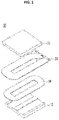
- FIG. 1 is an exploded perspective view showing an example of the configuration of a general slim-type transformer.
- a general slim-type transformer 10 includes a secondary coil 13 and a primary coil 14, which are provided between an upper core 11 and a lower core 12.
- the secondary coil 13 is composed of a plurality of conductive metal plates
- the primary coil 14 takes the form of a wound conductive wire.
- a bobbin (not shown) may be disposed between the upper core 11 and the lower core 12.
- FIG. 2A shows the relationship between a change in the height of the slim-type transformer and leakage inductance
- FIG. 2B shows the relationship between a change in the distance between the primary coil and the secondary coil and parasitic capacitance.
- a method of additionally providing a separate inductor including a core and a coil may be proposed.
- the reason for this is that the LC resonant circuit is transformed into an LLC resonant circuit, in which an operating-frequency-dependent gain change is smaller than in the LC resonant circuit.
- additional provision of an inductor entails a problem in that a separate space in the power supply unit (PSU) in which to mount the inductor is needed.
- parasitic capacitance increases sharply.
- the distance between the primary coil 14 and the secondary coil 13 is 200 ⁇ m or less
- the magnitude of the parasitic capacitance is 100 pF or greater.
- performance deteriorates due to electrical coupling, for example, voltage increases at low power, insulation is damaged, and electromagnetic interference (EMI) characteristics deteriorate.
- EMI electromagnetic interference
- the configuration of the secondary coil 13 may be modified from a conductive metal plate type to a conductive wire type.
- a larger space for accommodating the secondary coil is required inside the cores 11 and 12, leading to an increase in the height of the transformer.
- magnetic flux density in the cores increases, leading to generation of a larger amount of heat.
- a technical task of the present disclosure is to provide a slim-type transformer capable of being further miniaturized and a flat panel display device using the same.
- a technical task of the present disclosure is to provide a slim-type transformer capable of being miniaturized while securing leakage inductance and a flat panel display device using the same.
- a technical task of the present disclosure is to provide a slim-type transformer capable of being miniaturized while reducing parasitic capacitance and a flat panel display device using the same.
- a transformer may include a core unit having an upper core and a lower core, and a coil unit disposed in the core unit.
- the coil unit may include a first coil wound in a first direction, a second coil wound in a second direction, which is opposite the first direction, and a third coil having a flat plate shape.
- the lower core may include a body portion, first and second leg portions protruding from the body portion, and a spacing portion formed between the first leg portion and the second leg portion.
- the first leg portion may include two first outer legs and a first center leg disposed between the two first outer legs, and the second leg portion may include two second outer legs and a second center leg disposed between the two second outer legs.
- the first coil may be disposed to surround the first center leg, and the second coil may be disposed to surround the second center leg.
- the second coil may be disposed on the first coil such that a portion of the second coil overlaps the first coil in the thickness direction.
- the third coil may be disposed to surround the first center leg.
- first coil and the second coil may have ends led out toward a first side
- third coil may have ends led out toward a second side, which is opposite the first side
- At least one of the first coil to the third coil may have a portion protruding outwards beyond the core unit.
- the two first outer legs and the two second outer legs may be disposed parallel to each other on a plane, and the first center leg and the second center leg may be disposed parallel to each other on a plane.
- the first leg portion may have a total planar area greater than the total planar area of the second leg portion.
- the ratio of the planar areas of the two first outer legs to the planar area of the first center leg or the ratio of the planar areas of the two second outer legs to the planar area of the second center leg may be 0.65 to 0.8.
- the ratio of the planar area of the second leg portion to the planar area of the core unit may be 0.04 to 0.08.
- an insulating layer may be further disposed between the first coil and the second coil.
- an insulating layer may be further disposed between the first coil and the third coil.
- the transformer may further include a bobbin disposed in the core unit.
- At least one of the upper core or the lower core may have a recess formed between the first center leg and the second center leg.
- the transformer may further include a core shorting unit configured to electrically short the upper core and the lower core.
- a circuit board may include a substrate, a circuit portion formed on the substrate, and a transformer conductively connected to the circuit portion.
- the transformer may include a core unit having an upper core and a lower core, and a coil unit disposed in the core unit.
- the coil unit may include a first coil wound in a first direction, a second coil wound in a second direction, which is opposite the first direction, and a third coil having a flat plate shape.
- the upper core may include a body portion, first and second leg portions protruding from the body portion, and a spacing portion formed between the first leg portion and the second leg portion.
- the first leg portion may include two first outer legs and a first center leg disposed between the two first outer legs, and the second leg portion may include two second outer legs and a second center leg disposed between the two second outer legs.
- the first coil may be disposed to surround the first center leg, and the second coil may be disposed to surround the second center leg.
- a transformer according to an embodiment is provided therein with an inductor for securing leakage inductance through core sharing, and thus is capable of being reduced in size. Accordingly, a flat panel display device including the transformer is also capable of being slimmed.
- parasitic capacitance may be lowered by virtue of a core shorting unit for shorting one core and another core, thereby making it possible to prevent deterioration in performance due to electrical coupling.
- FIG. 3 is an exploded perspective view showing an example of the configuration of a transformer according to an embodiment
- FIG. 4 shows an example of the configuration of a core according to an embodiment.
- FIG. 3 For convenience of explanation, illustration of a bobbin is omitted from FIG. 3 , and an example of the configuration of the bobbin will be described later with reference to FIG. 5 .
- a transformer 100 may include cores 111 and 112 and coils 120, 130, and 140.
- the coils 120, 130, and 140 may include a primary coil 120, a secondary coil unit 130, and an inductor coil 140.
- the respective components will be described in detail.
- the cores 111 and 112 may have the function of a magnetic circuit, and may serve as a path for magnetic flux.
- the cores 111 and 112 may include an upper core 111, which is disposed at an upper position, and a lower core 112, which is disposed at a lower position.
- the two cores 111 and 112 may be formed to be symmetrical or asymmetrical to each other in a vertical direction. However, for convenience of explanation, the following description will be made on the assumption that the two cores are formed to be vertically symmetrical to each other, and thus only one of the two cores, e.g. the upper core 111, is illustrated in FIG. 4 .
- At least one of the upper core 111 or the lower core 112, which constitutes the cores 111 and 112, may include a body, which has a flat plate shape, and a plurality of leg portions, which protrude from the body in the thickness direction and extend in a predetermined direction.
- the plurality of leg portions may include first leg portions, which include two first outer legs TOL1 and TOL2, which extend in one axial direction (e.g. a y-axis direction) on a flat surface and are spaced apart from each other in another axis direction (e.g.
- first center leg TCL which is disposed between the two first outer legs TOL1 and TOL2
- second leg portions which include two second outer legs IOL1 and IOL2, which extend in one axial direction (e.g. the y-axis direction) and are spaced apart from each other in another axis direction (e.g. the x-axis direction), and one second center leg ICL, which is disposed between the two second outer legs.
- the first leg portions and the second leg portions may be spaced apart from each other, and thus gaps, i.e. spacing portions, may be formed therebetween.
- the first leg portions TOL1, TCL, and TOL2 mainly function as cores of the transformer
- the second leg portions IOL1, ICL, and IOL2 mainly function as cores of the inductor for securing leakage inductance.
- each of the cores 111 and 112 is implemented as having a single-body (i.e. integral-type) structure, the same performs the functions of cores of two magnetic elements, i.e. the transformer and the inductor.
- the above structure facilitates miniaturization of the transformer compared to a structure in which a core only for the transformer and a core only for the inductor are provided separately from each other.
- the four outer legs TOL1, TOL2, IOL1, and IOL2 may have the same width a1, but the disclosure is not limited thereto.
- the widths of the first outer legs TOL1 and TOL2, which mainly function as the transformer may be equal to each other, but may be different from the widths of the second outer legs IOL1 and IOL2, which mainly function as the inductor.
- the two center legs TCL and ICL may have the same width a2, but the disclosure is not limited thereto.
- the two center legs TCL and ICL may have different widths.
- the first leg portions TOL1, TCL, and TOL2, which mainly function as cores of the transformer, and the second leg portions IOL1, ICL, and IOL2, which mainly function as cores of the inductor, may be spaced apart from each other by a predetermined distance b2 in one direction (the y-axis direction), and thus spacing portions may be formed between the two first outer legs TOL1 and TOL2 and the two second outer legs IOL1 and IOL2 and between the first center leg TCL and the second center leg ICL.
- the spacing portions may serve as boundaries for preventing extension of the center legs and the outer legs in the y-axis direction and isolating a portion of the core that mainly functions as the inductor and a portion of the core that mainly functions as the transformer from each other.
- the center-leg spacing portion formed between the first center leg TCL and the second center leg ICL at least a portion of the primary coil 120 and at least a portion of the inductor coil 140 may overlap each other in the thickness direction (i.e. a z-axis direction).
- the structure in which the two coils 120 and 140 overlap each other may be a structure in which a larger accommodation space is required in the thickness direction in the center-leg spacing portion, and may also be a structure in which a larger amount of heat is generated due to addition of the heat produced from the superimposed coils 120 and 140.
- At least one of the upper core 111 or the lower core 112 may have a recess RC formed in the middle of the center-leg spacing portion thereof. Due to formation of the recess RC, the thickness of the corresponding portion of the core is reduced, and thus a space in which to dispose coils is secured. In addition, a path along which heat is transferred upwards in the upper core 111 is shortened, and a path along which heat is transferred downwards in the lower core 112 is shortened, whereby heat dissipation performance may be improved.
- the recess RC formed in the upper core 111 is illustrated in FIG. 4 as being recessed in the z-axis direction and having a rectangular planar shape, the disclosure is not limited thereto. Furthermore, it will be apparent to those skilled in the art that the recess may have any of various sizes.
- the ratio of the sum of the planar areas of the four outer legs TOL1, TOL2, IOL1, and IOL2 and the two center legs TCL and ICL to the overall planar area (i.e. a*b) of the upper core may be 0.15 to 0.30. Accordingly, the ratio of the planar area of the remaining region (hereinafter referred to as an "open region” or a "recess portion" for convenience of explanation), in which the outer legs or the center legs are not disposed, to the overall planar area of the upper core may be 0.7 to 0.85.
- the ratio of the areas of the outer legs to the area of the center leg corresponds to a2:2*a1, which may be 0.65 to 0.8, but the disclosure is not limited thereto.
- a magnetic path which is formed by winding a wire, is mainly formed around the center legs.
- the total planar area of the first leg portions TCL, TOL1, and TOL2 may be greater than the total planar area of the second leg portions ICL, IOL1, and IOL2.
- the ratio of the planar area of the inductor portion, which mainly functions as the inductor, to the overall planar area of the core, i.e. b:b3, may be 0.04 to 0.08, but the disclosure is not limited thereto. When this area ratio increases, series inductance increases.
- the area ratios described above are values obtained on the assumption that the turn ratio between the primary coil 120 and the inductor coil 140 is 1:1. However, it will be apparent to those skilled in the art that the turn ratio between the coils can be varied as appropriate.
- each of the four outer legs TOL1, TOL2, IOL1, and IOL2 and the two center legs TCL and ICL of the upper core 111 faces a corresponding one of the outer legs and the center legs of the lower core 112.
- a gap having a predetermined distance e.g. 10 to 100 ⁇ m without being limited thereto
- two pairs of center legs and four pairs of outer legs may be formed, and thus a maximum of six gaps may be formed.
- any of various specifications may be realized by controlling the positions at which the gaps are formed and the number of gaps.
- gaps are formed at a total of four points, specifically, between the pair of center legs TCL, which mainly function as the transformer, between the pair of center legs ICL, which mainly function as the inductor, between the pair of outer legs IOL1, and between the pair of outer legs IOL2, it may be advantageous for maintenance of inductance variation.
- all of the six gaps when all of the six gaps are formed, it may be advantageous from the aspect of heat generation characteristics because heat-generating portions are distributed to the maximum extent.
- Each gap may be formed in a manner such that a spacer, which has a predetermined thickness and is insulative, is interposed between the center legs or the outer legs that face each other, but the disclosure is not limited thereto.
- each of the cores 111 and 112 may include a magnetic material, for example, iron or ferrite, but the disclosure is not limited thereto.
- the primary coil 120 may be wound around the center leg TCL that mainly functions as the transformer, and the inductor coil 140 may be wound around the center leg ICL that mainly functions as the inductor.
- Insulating layers may be disposed on and under each of the coils 120 and 140 so that the coils 120 and 140 are insulated from the cores 111 and 112 and other coils 120, 130, and 140 adjacent thereto.
- the insulating layer may include at least one of ketone, a polyimide-based material, polyethylene terephthalate (PET), silicone, or an epoxy-based material, but the disclosure is not limited thereto.
- Each of the primary coil 120 and the inductor coil 140 may be a multiple-turn winding in which a rigid metallic conductor, for example, a copper conductive wire, is wound multiple times in a spiral or planar spiral shape, but the disclosure is not limited thereto.
- a rigid metallic conductor for example, a copper conductive wire
- TIW triple insulated wire
- the secondary coil unit 130 may include a first plate 131 and a second plate 132, each of which has a flat plate shape.
- Each of the first plate 131 and the second plate 132 may include a conductive metal (e.g. copper or aluminum), and may have a planar shape that is bilaterally symmetrical to the other of the first plate 131 and the second plate 132, but the disclosure is not limited thereto.
- Each of the first plate 131 and the second plate 132 may be turned once around the center leg TCL, which mainly functions as the transformer.
- the first plate 131 and the second plate 132 may be stacked, with the aforementioned insulating layer interposed therebetween. The ends of the plates 131 and 132 may be led out in the same direction.
- the direction in which the ends of the plates 131 and 132 are led out may preferably be opposite the direction in which the four ends of the two conductive wires, each of which constitutes a corresponding one of the primary coil 120 and the inductor coil 140, are led out, but the disclosure is not limited thereto.
- a portion of at least one of the above-described coils 120, 130, and 140 may protrude outwards beyond the cores 111 and 112.
- FIG. 5 shows an example of the shape of a bobbin according to an embodiment. Unlike FIG. 2 , illustration of the primary coil 120, the secondary coil unit 130, and the inductor coil 140 is omitted from FIG. 5 , and a bobbin 150 is additionally illustrated in FIG. 5 .
- the bobbin 150 may be disposed between the upper core 111 and the lower core 112.
- the bobbin 150 may include an upper plate 151, a lower plate 152, a first bore 153, a second bore 154, a first terminal T1, and a second terminal T2.
- the upper plate 151 and the lower plate 152 may be spaced apart from each other by a predetermined distance in the thickness direction (i.e. the z-axis direction), and the primary coil 120 and the inductor coil 140 may be wound and accommodated in this space.
- the ends of the conductive wires, each of which constitutes a corresponding one of the primary coil 120 and the inductor coil 140 are led out in the same direction, each of the led-out ends may be conductively connected to a corresponding one of a plurality of individual terminals, which constitute the first terminal T1.
- the lower plate 152 may be provided with a slope portion 155, which is disposed adjacent to the first bore 152 and forms passages inclined at a predetermined angle in order to guide the ends of the conductive wires constituting the primary coil 120 and the inductor coil 140 to the first terminal T1.
- the slope portion 155 the ends of the conductive wires that are led out toward the first terminal T1 do not occupy the space between the upper plate 151 and the lower plate 152 in the thickness direction without a turn, whereby the number of windings may be increased.
- the secondary coil unit 130 may be disposed on the bottom surface of the lower plate 152, and the ends of the first plate 131 and the second plate 132, which constitute the secondary coil unit 130, may be conductively connected to the second terminal T2. That is, by virtue of the lower plate 152, the secondary coil unit 130 is spaced apart from the primary coil 120 and the inductor coil 140 by a distance equal to at least the thickness of the lower plate 152, whereby sufficient distance for insulation is secured.
- Each of the plurality of individual terminals which constitute the first terminal T1 and the second terminal T2, may have a flange-type structure, in which the same extends at a predetermined slope to a predetermined height in a direction away from the center of the bobbin 150 and is then bent in the vertical direction. Due to this flange-type structure, the transformer 100 may be mounted in a bore formed in a substrate of the power supply unit (PSU), thereby reducing the influence of the height of the transformer 100 in the power supply unit (PSU), thus further contributing to the manufacture of a slimmer device.
- the power supply unit (PSU) may include a circuit board, which includes a substrate and a circuit portion formed on the substrate, and the transformer 100 may be conductively connected to the circuit portion on the circuit board.
- center leg ICL that mainly functions as the inductor of the cores 111 and 112 may pass through the first bore 153
- center leg TCL that mainly functions as the transformer of the cores 111 and 112 may pass through the second bore 154.
- FIG. 6A is a view for explaining the winding direction of the transformer according to an embodiment
- FIG. 6B is a view for explaining the effect of the winding direction of the transformer according to an embodiment.
- the primary coil 120 and the inductor coil 140 may be wound in opposite directions.
- the primary coil 120 may be wound in the clockwise direction, and the inductor coil 140 may be wound in the counterclockwise direction.
- this is illustrative.
- the primary coil 120 may be wound in the counterclockwise direction, and the inductor coil 140 may be wound in the clockwise direction. The reason why the winding directions of the primary coil 120 and the inductor coil 140 are opposite each other will be described with reference to FIG. 6B .
- inductance of 4100 ⁇ H was generated when each of the primary coil 120 and the inductor coil 140 was wound thirteen turns
- inductance of 3610 ⁇ H was generated when each of the primary coil 120 and the inductor coil 140 was wound twelve turns.
- a heat dissipation unit may be disposed on each of the cores 111 and 112 in order to improve heat dissipation performance. This will be described with reference to FIG. 7 .
- FIG. 7 is a view for explaining a heat dissipation unit of the transformer according to an embodiment.
- a heat dissipation unit 160 may be disposed in the open region of at least one of the upper core 111 or the lower core 112, which constitutes the cores 111 and 112, for example, the open region of the lower surface of the upper core 111 and/or the open region of the upper surface of the lower core 112.
- the heat dissipation unit 160 may be formed in the shape of a film that includes a material having excellent heat resistance and heat conductivity, for example, at least one of graphite or a sheet of polyimide (PI) (Kapton) tape, but the disclosure is not limited thereto.
- the heat dissipation unit 160 may extend to the outside of each of the cores 111 and 112 so as to be in contact with a housing of the power supply unit (PSU) or a heat sink, thereby contributing to rapid dissipation of the heat generated inside the transformer 100.
- PSU power supply unit
- the transformer may further include a core shorting unit (not shown) in order to control parasitic capacitance, which increases as the vertical distance between the primary coil 120 and the secondary coil unit 130 decreases.
- the core shorting unit may be disposed on one or both of the surfaces of the cores 111 and 112 that face each other, and may function to electrically short the upper core 111 and the lower core 112.
- at least a portion of the core shorting unit may be in contact with (that is, conductively connected to) the upper core 111, and at least part of the remaining portion thereof, other than the portion contacting the upper core 111, may be in contact with the lower core 112.
- the core shorting unit may include a conductive material in order to short the upper core 111 and the lower core 112, and may take the form of a thin film in order to make the transformer slim, but the disclosure is not limited thereto.
- the core shorting unit may be a copper foil, or may take the form of a conductive wire having a circular-shaped or polygonal-shaped cross-section.
- the core shorting unit may take the form of a thin film having a planar shape that is polygonal, other than rectangular, or circular.
Abstract
Description
- The present disclosure relates to a transformer and a flat panel display device including the same.
- In general, driving power is required in order to drive an electronic device, and a power supply device, such as a power supply unit (PSU), is essentially used in order to supply driving power to the electronic device.
- In particular, a display device, such as a flat panel TV, is required to be slim, and is continually being embodied in increasingly large sizes. Accordingly, it is necessary to reduce the thickness of such a large-scale display while meeting the increased power requirements thereof.
- A transformer occupies a larger volume in the power supply unit (PSU) than other elements. Therefore, one of the most important issues for a slim device is to reduce the thickness of the transformer.
-
FIG. 1 is an exploded perspective view showing an example of the configuration of a general slim-type transformer. - Referring to
FIG. 1 , a general slim-type transformer 10 includes asecondary coil 13 and aprimary coil 14, which are provided between anupper core 11 and alower core 12. In general, thesecondary coil 13 is composed of a plurality of conductive metal plates, and theprimary coil 14 takes the form of a wound conductive wire. In another configuration, a bobbin (not shown) may be disposed between theupper core 11 and thelower core 12. - However, when the thickness of the transformer is reduced to a certain value (e.g. 11 mm) or less, there is a problem in that performance deteriorates significantly due to the characteristics of leakage inductance and parasitic capacitance. This will be described with reference to
FIGs. 2A and 2B . -
FIG. 2A shows the relationship between a change in the height of the slim-type transformer and leakage inductance, andFIG. 2B shows the relationship between a change in the distance between the primary coil and the secondary coil and parasitic capacitance. - First, referring to
FIG. 2A , although there is a slight difference depending on the relative size of a gap formed between contact portions (generally, center legs) of theupper core 11 and thelower core 12, when the height of the transformer, for example, the distance from the upper surface of theupper core 11 to the lower surface of thelower core 12, is 13 mm or less, the leakage inductance becomes very low. Low leakage inductance is not preferable because performance fluctuates greatly depending on variation in load. The reason for this is that an LC resonant circuit constituted by the transformer in the power supply unit (PSU) operates in a relatively narrow band of operating frequencies, and accordingly, gain varies greatly depending on the amount of power that is used. In order to secure sufficient leakage inductance to prevent problems caused by low leakage inductance, a method of additionally providing a separate inductor including a core and a coil may be proposed. The reason for this is that the LC resonant circuit is transformed into an LLC resonant circuit, in which an operating-frequency-dependent gain change is smaller than in the LC resonant circuit. However, additional provision of an inductor entails a problem in that a separate space in the power supply unit (PSU) in which to mount the inductor is needed. - In addition, referring to
FIG. 2B , when the vertical distance between theprimary coil 14 and thesecondary coil 13 decreases, parasitic capacitance increases sharply. For example, when the distance between theprimary coil 14 and thesecondary coil 13 is 200 µm or less, the magnitude of the parasitic capacitance is 100 pF or greater. In a general slim-type transformer, when the magnitude of the parasitic capacitance is 100 pF or greater, performance deteriorates due to electrical coupling, for example, voltage increases at low power, insulation is damaged, and electromagnetic interference (EMI) characteristics deteriorate. - In order to reduce parasitic capacitance, the configuration of the
secondary coil 13 may be modified from a conductive metal plate type to a conductive wire type. However, when the secondary coil is formed in a conductive wire type, a larger space for accommodating the secondary coil is required inside thecores cores - A technical task of the present disclosure is to provide a slim-type transformer capable of being further miniaturized and a flat panel display device using the same.
- Particularly, a technical task of the present disclosure is to provide a slim-type transformer capable of being miniaturized while securing leakage inductance and a flat panel display device using the same.
- In addition, a technical task of the present disclosure is to provide a slim-type transformer capable of being miniaturized while reducing parasitic capacitance and a flat panel display device using the same.
- The technical tasks of the present disclosure are not limited to the above-mentioned technical tasks, and other technical tasks not mentioned herein will be clearly understood by those skilled in the art from the following description.
- A transformer according to an embodiment may include a core unit having an upper core and a lower core, and a coil unit disposed in the core unit. The coil unit may include a first coil wound in a first direction, a second coil wound in a second direction, which is opposite the first direction, and a third coil having a flat plate shape. The lower core may include a body portion, first and second leg portions protruding from the body portion, and a spacing portion formed between the first leg portion and the second leg portion. The first leg portion may include two first outer legs and a first center leg disposed between the two first outer legs, and the second leg portion may include two second outer legs and a second center leg disposed between the two second outer legs. The first coil may be disposed to surround the first center leg, and the second coil may be disposed to surround the second center leg.
- In an example, the second coil may be disposed on the first coil such that a portion of the second coil overlaps the first coil in the thickness direction.
- In an example, the third coil may be disposed to surround the first center leg.
- In an example, the first coil and the second coil may have ends led out toward a first side, and the third coil may have ends led out toward a second side, which is opposite the first side.
- In an example, at least one of the first coil to the third coil may have a portion protruding outwards beyond the core unit.
- In an example, the two first outer legs and the two second outer legs may be disposed parallel to each other on a plane, and the first center leg and the second center leg may be disposed parallel to each other on a plane.
- In an example, the first leg portion may have a total planar area greater than the total planar area of the second leg portion.
- In an example, the ratio of the planar areas of the two first outer legs to the planar area of the first center leg or the ratio of the planar areas of the two second outer legs to the planar area of the second center leg may be 0.65 to 0.8.
- In an example, the ratio of the planar area of the second leg portion to the planar area of the core unit may be 0.04 to 0.08.
- In an example, an insulating layer may be further disposed between the first coil and the second coil.
- In an example, an insulating layer may be further disposed between the first coil and the third coil.
- In an example, the transformer may further include a bobbin disposed in the core unit.
- In an example, at least one of the upper core or the lower core may have a recess formed between the first center leg and the second center leg.
- In an example, the transformer may further include a core shorting unit configured to electrically short the upper core and the lower core.
- In addition, a circuit board according to an embodiment may include a substrate, a circuit portion formed on the substrate, and a transformer conductively connected to the circuit portion. The transformer may include a core unit having an upper core and a lower core, and a coil unit disposed in the core unit. The coil unit may include a first coil wound in a first direction, a second coil wound in a second direction, which is opposite the first direction, and a third coil having a flat plate shape. The upper core may include a body portion, first and second leg portions protruding from the body portion, and a spacing portion formed between the first leg portion and the second leg portion. The first leg portion may include two first outer legs and a first center leg disposed between the two first outer legs, and the second leg portion may include two second outer legs and a second center leg disposed between the two second outer legs. The first coil may be disposed to surround the first center leg, and the second coil may be disposed to surround the second center leg.
- A transformer according to an embodiment is provided therein with an inductor for securing leakage inductance through core sharing, and thus is capable of being reduced in size. Accordingly, a flat panel display device including the transformer is also capable of being slimmed.
- In addition, according to the present disclosure, parasitic capacitance may be lowered by virtue of a core shorting unit for shorting one core and another core, thereby making it possible to prevent deterioration in performance due to electrical coupling.
- The effects achievable through the present disclosure are not limited to the above-mentioned effects, and other effects not mentioned herein will be clearly understood by those skilled in the art from the following description.
-
-
FIG. 1 is an exploded perspective view showing an example of the configuration of a general slim-type transformer. -
FIG. 2A shows the relationship between a change in the height of the slim-type transformer and leakage inductance, andFIG. 2B shows the relationship between a change in the distance between a primary coil and a secondary coil and parasitic capacitance. -
FIG. 3 is an exploded perspective view showing an example of the configuration of a transformer according to an embodiment. -
FIG. 4 shows an example of the configuration of a core according to an embodiment. -
FIG. 5 shows an example of the shape of a bobbin according to an embodiment. -
FIG. 6A is a view for explaining the winding direction of the transformer according to an embodiment. -
FIG. 6B is a view for explaining the effect of the winding direction of the transformer according to an embodiment. -
FIG. 7 is a view for explaining a heat dissipation unit of the transformer according to an embodiment. - The present disclosure will now be described more fully hereinafter with reference to the accompanying drawings, in which various embodiments are shown. The examples, however, may be embodied in many different forms and should not be construed as being limited to the embodiments set forth herein. It is to be understood that the present disclosure covers all modifications, equivalents, and alternatives falling within the scope and spirit of the present disclosure.
- While ordinal numbers including "second", "first", etc. may be used to describe various components, they are not intended to limit the components. These expressions are used only to distinguish one component from another component. For example, a second element could be termed a first element, and, similarly, a first element could be termed a second element, without departing from the scope of the present disclosure. As used herein, the term "and/or" includes any and all combinations of one or more of the associated listed items.
- It will be understood that when an element is referred to as being "connected" or "coupled" to another element, it can be directly connected or coupled to the other element, or intervening elements may be present. In contrast, when an element is referred to as being "directly connected" or "directly coupled" to another element, there are no intervening elements present.
- In the description of the embodiments, it will be understood that when an element, such as a layer (film), a region, a pattern or a structure, is referred to as being "on" or "under" another element, such as a substrate, a layer (film), a region, a pad or a pattern, the term "on" or "under" means that the element is "directly" on or under another element or is "indirectly" formed such that an intervening element may also be present. It will also be understood that criteria of on or under is on the basis of the drawing. In addition, the thickness or size of a layer (film), a region, a pattern or a structure shown in the drawings may be exaggerated, omitted or schematically drawn for the clarity and convenience of explanation, and may not accurately reflect the actual size.
- The terminology used herein is for the purpose of describing particular embodiments only and is not intended to be limiting of exemplary embodiments of the disclosure. As used herein, the singular forms are intended to include the plural forms as well, unless the context clearly indicates otherwise. It will be further understood that the term "include" or "have", when used herein, specifies the presence of stated features, integers, steps, operations, elements, components, or combinations thereof, but do not preclude the presence or addition of one or more other features, integers, steps, operations, elements, components, or combinations thereof.
- Unless otherwise defined, all terms used herein, which include technical or scientific terms, have the same meanings as those generally appreciated by those skilled in the art. The terms, such as ones defined in common dictionaries, should be interpreted as having the same meanings as terms in the context of pertinent technology, and should not be interpreted as having ideal or excessively formal meanings unless clearly defined in the specification.
- Hereinafter, a transformer according to an embodiment will be described in detail with reference to the accompanying drawings.
-
FIG. 3 is an exploded perspective view showing an example of the configuration of a transformer according to an embodiment, andFIG. 4 shows an example of the configuration of a core according to an embodiment. - For convenience of explanation, illustration of a bobbin is omitted from
FIG. 3 , and an example of the configuration of the bobbin will be described later with reference toFIG. 5 . - Referring to
FIGs. 3 and4 together, atransformer 100 according to an embodiment may includecores coils primary coil 120, asecondary coil unit 130, and aninductor coil 140. Hereinafter, the respective components will be described in detail. - The
cores cores upper core 111, which is disposed at an upper position, and alower core 112, which is disposed at a lower position. The twocores upper core 111, is illustrated inFIG. 4 . - At least one of the
upper core 111 or thelower core 112, which constitutes thecores - Here, the first leg portions TOL1, TCL, and TOL2 mainly function as cores of the transformer, and the second leg portions IOL1, ICL, and IOL2 mainly function as cores of the inductor for securing leakage inductance. In other words, although each of the
cores - The four outer legs TOL1, TOL2, IOL1, and IOL2 may have the same width a1, but the disclosure is not limited thereto. In an example, the widths of the first outer legs TOL1 and TOL2, which mainly function as the transformer, may be equal to each other, but may be different from the widths of the second outer legs IOL1 and IOL2, which mainly function as the inductor. In addition, the two center legs TCL and ICL may have the same width a2, but the disclosure is not limited thereto. In an example, the two center legs TCL and ICL may have different widths.
- The first leg portions TOL1, TCL, and TOL2, which mainly function as cores of the transformer, and the second leg portions IOL1, ICL, and IOL2, which mainly function as cores of the inductor, may be spaced apart from each other by a predetermined distance b2 in one direction (the y-axis direction), and thus spacing portions may be formed between the two first outer legs TOL1 and TOL2 and the two second outer legs IOL1 and IOL2 and between the first center leg TCL and the second center leg ICL.
- In this case, the spacing portions may serve as boundaries for preventing extension of the center legs and the outer legs in the y-axis direction and isolating a portion of the core that mainly functions as the inductor and a portion of the core that mainly functions as the transformer from each other.
- Among the spacing portions, in the center-leg spacing portion formed between the first center leg TCL and the second center leg ICL, as shown in
FIG. 6A , at least a portion of theprimary coil 120 and at least a portion of theinductor coil 140 may overlap each other in the thickness direction (i.e. a z-axis direction). The structure in which the twocoils coils upper core 111 or thelower core 112 may have a recess RC formed in the middle of the center-leg spacing portion thereof. Due to formation of the recess RC, the thickness of the corresponding portion of the core is reduced, and thus a space in which to dispose coils is secured. In addition, a path along which heat is transferred upwards in theupper core 111 is shortened, and a path along which heat is transferred downwards in thelower core 112 is shortened, whereby heat dissipation performance may be improved. Although the recess RC formed in theupper core 111 is illustrated inFIG. 4 as being recessed in the z-axis direction and having a rectangular planar shape, the disclosure is not limited thereto. Furthermore, it will be apparent to those skilled in the art that the recess may have any of various sizes. - Meanwhile, in the case of one of the
cores upper core 111 shown inFIG. 4 , the ratio of the sum of the planar areas of the four outer legs TOL1, TOL2, IOL1, and IOL2 and the two center legs TCL and ICL to the overall planar area (i.e. a*b) of the upper core may be 0.15 to 0.30. Accordingly, the ratio of the planar area of the remaining region (hereinafter referred to as an "open region" or a "recess portion" for convenience of explanation), in which the outer legs or the center legs are not disposed, to the overall planar area of the upper core may be 0.7 to 0.85. - When the ratio of the planar areas of the outer legs and the center legs to the overall planar area increases, series inductance increases, and the magnetizing inductance of the transformer decreases. In contrast, when the ratio of the planar area of the open region to the overall planar area increases, series inductance decreases, and the magnetizing inductance of the transformer increases.
- The ratio of the areas of the outer legs to the area of the center leg corresponds to a2:2*a1, which may be 0.65 to 0.8, but the disclosure is not limited thereto. The reason for this is that a magnetic path, which is formed by winding a wire, is mainly formed around the center legs.
- In addition, the total planar area of the first leg portions TCL, TOL1, and TOL2 may be greater than the total planar area of the second leg portions ICL, IOL1, and IOL2.
- In addition, the ratio of the planar area of the inductor portion, which mainly functions as the inductor, to the overall planar area of the core, i.e. b:b3, may be 0.04 to 0.08, but the disclosure is not limited thereto. When this area ratio increases, series inductance increases.
- The area ratios described above are values obtained on the assumption that the turn ratio between the
primary coil 120 and theinductor coil 140 is 1:1. However, it will be apparent to those skilled in the art that the turn ratio between the coils can be varied as appropriate. - When the
upper core 111 and thelower core 112 are vertically coupled to each other, each of the four outer legs TOL1, TOL2, IOL1, and IOL2 and the two center legs TCL and ICL of theupper core 111 faces a corresponding one of the outer legs and the center legs of thelower core 112. In this case, a gap having a predetermined distance (e.g. 10 to 100 µm without being limited thereto) may be formed between at least one pair among the pairs of outer legs and the pairs of center legs, which face each other. In other words, when theupper core 111 and thelower core 112 are coupled to each other, two pairs of center legs and four pairs of outer legs may be formed, and thus a maximum of six gaps may be formed. Therefore, there is an advantage in that any of various specifications may be realized by controlling the positions at which the gaps are formed and the number of gaps. In an example, when gaps are formed at a total of four points, specifically, between the pair of center legs TCL, which mainly function as the transformer, between the pair of center legs ICL, which mainly function as the inductor, between the pair of outer legs IOL1, and between the pair of outer legs IOL2, it may be advantageous for maintenance of inductance variation. In another example, when all of the six gaps are formed, it may be advantageous from the aspect of heat generation characteristics because heat-generating portions are distributed to the maximum extent. Each gap may be formed in a manner such that a spacer, which has a predetermined thickness and is insulative, is interposed between the center legs or the outer legs that face each other, but the disclosure is not limited thereto. - Meanwhile, each of the
cores - The
primary coil 120 may be wound around the center leg TCL that mainly functions as the transformer, and theinductor coil 140 may be wound around the center leg ICL that mainly functions as the inductor. Insulating layers (not shown) may be disposed on and under each of thecoils coils cores other coils - Each of the
primary coil 120 and theinductor coil 140 may be a multiple-turn winding in which a rigid metallic conductor, for example, a copper conductive wire, is wound multiple times in a spiral or planar spiral shape, but the disclosure is not limited thereto. For example, an enamel wire (USTC wire) wrapped by a fiber yarn, a Litz wire, a triple insulated wire (TIW), or the like may be used for each of thecoils - Four ends of the two conductive wires, each of which constitutes a corresponding one of the
primary coil 120 and theinductor coil 140, may be led out in the same direction. - The
secondary coil unit 130 may include afirst plate 131 and asecond plate 132, each of which has a flat plate shape. Each of thefirst plate 131 and thesecond plate 132 may include a conductive metal (e.g. copper or aluminum), and may have a planar shape that is bilaterally symmetrical to the other of thefirst plate 131 and thesecond plate 132, but the disclosure is not limited thereto. Each of thefirst plate 131 and thesecond plate 132 may be turned once around the center leg TCL, which mainly functions as the transformer. Preferably, thefirst plate 131 and thesecond plate 132 may be stacked, with the aforementioned insulating layer interposed therebetween. The ends of theplates plates primary coil 120 and theinductor coil 140, are led out, but the disclosure is not limited thereto. - Meanwhile, a portion of at least one of the above-described
coils cores -
FIG. 5 shows an example of the shape of a bobbin according to an embodiment. UnlikeFIG. 2 , illustration of theprimary coil 120, thesecondary coil unit 130, and theinductor coil 140 is omitted fromFIG. 5 , and abobbin 150 is additionally illustrated inFIG. 5 . - Referring to
FIG. 5 , thebobbin 150 may be disposed between theupper core 111 and thelower core 112. Thebobbin 150 may include anupper plate 151, alower plate 152, afirst bore 153, asecond bore 154, a first terminal T1, and a second terminal T2. - The
upper plate 151 and thelower plate 152 may be spaced apart from each other by a predetermined distance in the thickness direction (i.e. the z-axis direction), and theprimary coil 120 and theinductor coil 140 may be wound and accommodated in this space. As described above, when the ends of the conductive wires, each of which constitutes a corresponding one of theprimary coil 120 and theinductor coil 140, are led out in the same direction, each of the led-out ends may be conductively connected to a corresponding one of a plurality of individual terminals, which constitute the first terminal T1. Here, thelower plate 152 may be provided with aslope portion 155, which is disposed adjacent to thefirst bore 152 and forms passages inclined at a predetermined angle in order to guide the ends of the conductive wires constituting theprimary coil 120 and theinductor coil 140 to the first terminal T1. By virtue of theslope portion 155, the ends of the conductive wires that are led out toward the first terminal T1 do not occupy the space between theupper plate 151 and thelower plate 152 in the thickness direction without a turn, whereby the number of windings may be increased. - The
secondary coil unit 130 may be disposed on the bottom surface of thelower plate 152, and the ends of thefirst plate 131 and thesecond plate 132, which constitute thesecondary coil unit 130, may be conductively connected to the second terminal T2. That is, by virtue of thelower plate 152, thesecondary coil unit 130 is spaced apart from theprimary coil 120 and theinductor coil 140 by a distance equal to at least the thickness of thelower plate 152, whereby sufficient distance for insulation is secured. - Each of the plurality of individual terminals, which constitute the first terminal T1 and the second terminal T2, may have a flange-type structure, in which the same extends at a predetermined slope to a predetermined height in a direction away from the center of the
bobbin 150 and is then bent in the vertical direction. Due to this flange-type structure, thetransformer 100 may be mounted in a bore formed in a substrate of the power supply unit (PSU), thereby reducing the influence of the height of thetransformer 100 in the power supply unit (PSU), thus further contributing to the manufacture of a slimmer device. Here, the power supply unit (PSU) may include a circuit board, which includes a substrate and a circuit portion formed on the substrate, and thetransformer 100 may be conductively connected to the circuit portion on the circuit board. - Meanwhile, the center leg ICL that mainly functions as the inductor of the
cores first bore 153, and the center leg TCL that mainly functions as the transformer of thecores second bore 154. - Hereinafter, the winding directions of the
first coil 120 and theinductor coil 140 will be described with reference toFIGs. 6A and6B . -
FIG. 6A is a view for explaining the winding direction of the transformer according to an embodiment, andFIG. 6B is a view for explaining the effect of the winding direction of the transformer according to an embodiment. - First, referring to
FIG. 6A , theprimary coil 120 and theinductor coil 140 according to the embodiment may be wound in opposite directions. In an example, theprimary coil 120 may be wound in the clockwise direction, and theinductor coil 140 may be wound in the counterclockwise direction. Of course, this is illustrative. Theprimary coil 120 may be wound in the counterclockwise direction, and theinductor coil 140 may be wound in the clockwise direction. The reason why the winding directions of theprimary coil 120 and theinductor coil 140 are opposite each other will be described with reference toFIG. 6B . - First, referring to the uppermost drawing in
FIG. 6B , when theprimary coil 120 is wound in the clockwise direction and theinductor coil 140 is wound in the counterclockwise direction, the direction of the magnetic flux generated by theprimary coil 120 and the direction of the magnetic flux generated by theinductor coil 140 are the same in each of the center legs, thus resulting in magnetic flux reinforcement. On the other hand, the direction of the magnetic flux generated by theprimary coil 120 and the direction of the magnetic flux generated by theinductor coil 140 are opposite each other in each of the outer legs, thus resulting in magnetic flux cancellation. According to experimentation performed under the above conditions, inductance of 4100 µH was generated when each of theprimary coil 120 and theinductor coil 140 was wound thirteen turns, and inductance of 3610 µH was generated when each of theprimary coil 120 and theinductor coil 140 was wound twelve turns. - On the other hand, referring to the intermediate drawing in
FIG. 6B , when the winding direction of theprimary coil 120 and the winding direction of theinductor coil 140 are the same, magnetic flux cancellation occurs in each of the center legs, and magnetic flux reinforcement occurs in each of the outer legs, unlike the case inFIG. 6A . According to experimentation performed under the above conditions, inductance of 1946 µH was generated when each of theprimary coil 120 and theinductor coil 140 was wound thirteen turns, and inductance of 1706 µH was generated when each of theprimary coil 120 and theinductor coil 140 was wound twelve turns. That is, compared to the case inFIG. 6A , in which the winding directions are opposite each other, inductance decreased remarkably. Consequently, it can be seen that it is preferable for the winding direction of theprimary coil 120 and the winding direction of theinductor coil 140 to be opposite each other in order to obtain a high leakage inductance value. - Meanwhile, referring to the lowermost drawing in
FIG. 6B , when the outer legs are formed in an integral type, although the winding direction of theprimary coil 120 and the winding direction of theinductor coil 140 are opposite each other, magnetic flux cancellation occurring in each of the outer legs has an effect on each of the center legs, thus degrading the reinforcement characteristics in each of the center legs. This case results not only in a decrease in leakage inductance value but also in an increase in the amount of heat that is generated. Therefore, it is preferable to form the spacing portions in order to avoid integration of the outer legs. - According to an embodiment of the present disclosure, a heat dissipation unit may be disposed on each of the
cores FIG. 7 . -
FIG. 7 is a view for explaining a heat dissipation unit of the transformer according to an embodiment. - Referring to
FIG. 7 , aheat dissipation unit 160 may be disposed in the open region of at least one of theupper core 111 or thelower core 112, which constitutes thecores upper core 111 and/or the open region of the upper surface of thelower core 112. Theheat dissipation unit 160 may be formed in the shape of a film that includes a material having excellent heat resistance and heat conductivity, for example, at least one of graphite or a sheet of polyimide (PI) (Kapton) tape, but the disclosure is not limited thereto. Theheat dissipation unit 160 may extend to the outside of each of thecores transformer 100. - On the other hand, according to another embodiment, the transformer may further include a core shorting unit (not shown) in order to control parasitic capacitance, which increases as the vertical distance between the
primary coil 120 and thesecondary coil unit 130 decreases. The core shorting unit may be disposed on one or both of the surfaces of thecores upper core 111 and thelower core 112. In order to realize a short circuit, at least a portion of the core shorting unit may be in contact with (that is, conductively connected to) theupper core 111, and at least part of the remaining portion thereof, other than the portion contacting theupper core 111, may be in contact with thelower core 112. Furthermore, the core shorting unit may include a conductive material in order to short theupper core 111 and thelower core 112, and may take the form of a thin film in order to make the transformer slim, but the disclosure is not limited thereto. In an example, the core shorting unit may be a copper foil, or may take the form of a conductive wire having a circular-shaped or polygonal-shaped cross-section. In another example, the core shorting unit may take the form of a thin film having a planar shape that is polygonal, other than rectangular, or circular. - While the present disclosure has been particularly shown and described with reference to exemplary embodiments thereof, these embodiments are only proposed for illustrative purposes and do not restrict the present disclosure, and it will be apparent to those skilled in the art that various changes in form and detail may be made without departing from the essential characteristics of the embodiments set forth herein. For example, respective configurations set forth in the embodiments may be modified and applied. Further, differences in such modifications and applications should be construed as falling within the scope of the present disclosure as defined by the appended claims.
Claims (10)
- A transformer comprising:a core unit having an upper core and a lower core; anda coil unit disposed in the core unit,wherein the coil unit comprises:a first coil wound in a first direction;a second coil wound in a second direction, the second direction being opposite the first direction; anda third coil having a flat plate shape,wherein the upper core comprises:a body portion;a first leg portion and a second leg portion protruding from the body portion; anda spacing portion formed between the first leg portion and the second leg portion,wherein the first leg portion comprises two first outer legs and a first center leg disposed between the two first outer legs,wherein the second leg portion comprises two second outer legs and a second center leg disposed between the two second outer legs,wherein the first coil is disposed to surround the first center leg, andwherein the second coil is disposed to surround the second center leg.
- The transformer according to claim 1, wherein the second coil is disposed on the first coil such that a portion of the second coil overlaps the first coil in a thickness direction.
- The transformer according to claim 2, wherein the third coil is disposed to surround the first center leg.
- The transformer according to claim 1, wherein the first coil and the second coil have ends led out toward a first side, and
wherein the third coil has ends led out toward a second side, the second side being opposite the first side. - The transformer according to claim 1, wherein at least one of the first coil to the third coil has a portion protruding outwards beyond the core unit.
- The transformer according to claim 1, wherein the two first outer legs and the two second outer legs are disposed parallel to each other on a plane, and
wherein the first center leg and the second center leg are disposed parallel to each other on a plane. - The transformer according to claim 1, wherein the first leg portion has a total planar area greater than a total planar area of the second leg portion.
- The transformer according to claim 6, wherein a ratio of planar areas of the two first outer legs to a planar area of the first center leg or a ratio of planar areas of the two second outer legs to a planar area of the second center leg is 0.65 to 0.8.
- The transformer according to claim 1, wherein a ratio of a planar area of the second leg portion to a planar area of the core unit is 0.04 to 0.08.
- The transformer according to claim 1, wherein at least one of the upper core or the lower core has a recess formed between the first center leg and the second center leg.
Applications Claiming Priority (2)
| Application Number | Priority Date | Filing Date | Title |
|---|---|---|---|
| KR1020200012155A KR20210098230A (en) | 2020-01-31 | 2020-01-31 | Transformer and flat panel display device including the same |
| PCT/KR2021/001240 WO2021154048A1 (en) | 2020-01-31 | 2021-01-29 | Transformer and flat panel display device including same |
Publications (2)
| Publication Number | Publication Date |
|---|---|
| EP4099349A1 true EP4099349A1 (en) | 2022-12-07 |
| EP4099349A4 EP4099349A4 (en) | 2024-03-13 |
Family
ID=77079743
Family Applications (1)
| Application Number | Title | Priority Date | Filing Date |
|---|---|---|---|
| EP21748056.5A Pending EP4099349A4 (en) | 2020-01-31 | 2021-01-29 | Transformer and flat panel display device including same |
Country Status (6)
| Country | Link |
|---|---|
| US (1) | US20230076761A1 (en) |
| EP (1) | EP4099349A4 (en) |
| JP (1) | JP2023514519A (en) |
| KR (1) | KR20210098230A (en) |
| CN (1) | CN115413361A (en) |
| WO (1) | WO2021154048A1 (en) |
Families Citing this family (2)
| Publication number | Priority date | Publication date | Assignee | Title |
|---|---|---|---|---|
| KR102603589B1 (en) * | 2021-08-12 | 2023-11-17 | 주식회사 엠에스티테크 | Coil component |
| US11842835B2 (en) * | 2021-12-08 | 2023-12-12 | Rompower Technology Holdings, Llc | High density magnetic structure |
Family Cites Families (7)
| Publication number | Priority date | Publication date | Assignee | Title |
|---|---|---|---|---|
| JP2770750B2 (en) * | 1994-10-03 | 1998-07-02 | ネミック・ラムダ株式会社 | Inductance element |
| JP2005093493A (en) * | 2003-09-12 | 2005-04-07 | Tamura Seisakusho Co Ltd | Low profile transformer and its manufacturing method |
| KR101105536B1 (en) * | 2010-06-04 | 2012-01-13 | 전주대학교 산학협력단 | Planar Transformer |
| KR101133584B1 (en) * | 2010-10-08 | 2012-04-05 | 전주대학교 산학협력단 | Planar transformer |
| KR101838225B1 (en) * | 2016-07-12 | 2018-03-13 | 이주열 | Double core planar transformer |
| KR102030570B1 (en) * | 2018-01-25 | 2019-10-10 | 주식회사 이랜텍 | Planar transformer and method for assembling thereof |
| KR101989172B1 (en) * | 2019-05-17 | 2019-06-14 | (주) 트랜스온 | Flat type transformer |
-
2020
- 2020-01-31 KR KR1020200012155A patent/KR20210098230A/en active Search and Examination
-
2021
- 2021-01-29 CN CN202180026531.6A patent/CN115413361A/en active Pending
- 2021-01-29 EP EP21748056.5A patent/EP4099349A4/en active Pending
- 2021-01-29 US US17/759,898 patent/US20230076761A1/en active Pending
- 2021-01-29 JP JP2022546660A patent/JP2023514519A/en active Pending
- 2021-01-29 WO PCT/KR2021/001240 patent/WO2021154048A1/en unknown
Also Published As
| Publication number | Publication date |
|---|---|
| EP4099349A4 (en) | 2024-03-13 |
| CN115413361A (en) | 2022-11-29 |
| KR20210098230A (en) | 2021-08-10 |
| JP2023514519A (en) | 2023-04-06 |
| US20230076761A1 (en) | 2023-03-09 |
| WO2021154048A1 (en) | 2021-08-05 |
Similar Documents
| Publication | Publication Date | Title |
|---|---|---|
| US8432245B2 (en) | Power module and circuit board assembly thereof | |
| US6847284B2 (en) | Planar coil and planar transformer | |
| US8378777B2 (en) | Magnetic electrical device | |
| US7439838B2 (en) | Transformers and winding units thereof | |
| US8054152B2 (en) | Transformer | |
| US8013710B2 (en) | Magnetic element module | |
| US7218199B1 (en) | Structure of transformer | |
| EP4099349A1 (en) | Transformer and flat panel display device including same | |
| US8570135B2 (en) | Transformer and display device using the same | |
| US8188825B2 (en) | Transformer structure | |
| US20110102119A1 (en) | Resonant transformer | |
| KR20230038159A (en) | Transformer and flat panel display device including the same | |
| KR20180007888A (en) | Common winding wire planar transformer | |
| KR102444844B1 (en) | Magnetic coupling device and flat panel display device including the same | |
| US20120139686A1 (en) | Magnetic device and assembling method thereof | |
| US20230282410A1 (en) | Transformer and flat panel display device comprising same | |
| KR20190014727A (en) | Dual Core Planar Transformer | |
| US20220301762A1 (en) | Electronic device | |
| US20240087800A1 (en) | Transformer | |
| JPH11307366A (en) | Thin transformer coil | |
| KR102513410B1 (en) | Transformer and flat panel display device including the same | |
| US20210287848A1 (en) | Coupled inductor and power module | |
| US20220028598A1 (en) | Magnetic induction assembly | |
| KR20210143514A (en) | Transformer and circuit board having the same | |
| CN115955832A (en) | Magnetic component with fringing field shielding |
Legal Events
| Date | Code | Title | Description |
|---|---|---|---|
| STAA | Information on the status of an ep patent application or granted ep patent |
Free format text: STATUS: THE INTERNATIONAL PUBLICATION HAS BEEN MADE |
|
| PUAI | Public reference made under article 153(3) epc to a published international application that has entered the european phase |
Free format text: ORIGINAL CODE: 0009012 |
|
| STAA | Information on the status of an ep patent application or granted ep patent |
Free format text: STATUS: REQUEST FOR EXAMINATION WAS MADE |
|
| 17P | Request for examination filed |
Effective date: 20220808 |
|
| AK | Designated contracting states |
Kind code of ref document: A1 Designated state(s): AL AT BE BG CH CY CZ DE DK EE ES FI FR GB GR HR HU IE IS IT LI LT LU LV MC MK MT NL NO PL PT RO RS SE SI SK SM TR |
|
| DAV | Request for validation of the european patent (deleted) | ||
| DAX | Request for extension of the european patent (deleted) | ||
| A4 | Supplementary search report drawn up and despatched |
Effective date: 20240213 |
|
| RIC1 | Information provided on ipc code assigned before grant |
Ipc: H01F 3/10 20060101ALI20240208BHEP Ipc: H01F 30/06 20060101AFI20240208BHEP |