EP4096370A1 - Wiring circuit board and method of producing the same - Google Patents
Wiring circuit board and method of producing the same Download PDFInfo
- Publication number
- EP4096370A1 EP4096370A1 EP22174581.3A EP22174581A EP4096370A1 EP 4096370 A1 EP4096370 A1 EP 4096370A1 EP 22174581 A EP22174581 A EP 22174581A EP 4096370 A1 EP4096370 A1 EP 4096370A1
- Authority
- EP
- European Patent Office
- Prior art keywords
- layer
- thickness direction
- porous insulating
- insulating layer
- ground
- Prior art date
- Legal status (The legal status is an assumption and is not a legal conclusion. Google has not performed a legal analysis and makes no representation as to the accuracy of the status listed.)
- Withdrawn
Links
- 238000000034 method Methods 0.000 title claims description 27
- 239000010410 layer Substances 0.000 claims description 465
- 239000012790 adhesive layer Substances 0.000 claims description 89
- 230000000149 penetrating effect Effects 0.000 claims description 58
- 239000004020 conductor Substances 0.000 claims description 43
- 238000003825 pressing Methods 0.000 claims description 4
- 239000000463 material Substances 0.000 description 16
- 230000002787 reinforcement Effects 0.000 description 16
- 230000002093 peripheral effect Effects 0.000 description 13
- 239000011347 resin Substances 0.000 description 9
- 229920005989 resin Polymers 0.000 description 9
- 238000000059 patterning Methods 0.000 description 6
- 229920001721 polyimide Polymers 0.000 description 6
- 230000015572 biosynthetic process Effects 0.000 description 5
- XEEYBQQBJWHFJM-UHFFFAOYSA-N Iron Chemical compound [Fe] XEEYBQQBJWHFJM-UHFFFAOYSA-N 0.000 description 4
- 239000009719 polyimide resin Substances 0.000 description 4
- 238000001039 wet etching Methods 0.000 description 4
- RYGMFSIKBFXOCR-UHFFFAOYSA-N Copper Chemical compound [Cu] RYGMFSIKBFXOCR-UHFFFAOYSA-N 0.000 description 3
- 229910052802 copper Inorganic materials 0.000 description 3
- 239000010949 copper Substances 0.000 description 3
- 230000000694 effects Effects 0.000 description 3
- 238000007747 plating Methods 0.000 description 3
- 229920000106 Liquid crystal polymer Polymers 0.000 description 2
- 239000004977 Liquid-crystal polymers (LCPs) Substances 0.000 description 2
- PXHVJJICTQNCMI-UHFFFAOYSA-N Nickel Chemical compound [Ni] PXHVJJICTQNCMI-UHFFFAOYSA-N 0.000 description 2
- 239000004642 Polyimide Substances 0.000 description 2
- 229910052782 aluminium Inorganic materials 0.000 description 2
- XAGFODPZIPBFFR-UHFFFAOYSA-N aluminium Chemical compound [Al] XAGFODPZIPBFFR-UHFFFAOYSA-N 0.000 description 2
- 238000001312 dry etching Methods 0.000 description 2
- 229910052742 iron Inorganic materials 0.000 description 2
- 229910052751 metal Inorganic materials 0.000 description 2
- 239000002184 metal Substances 0.000 description 2
- 150000002739 metals Chemical class 0.000 description 2
- 229910001220 stainless steel Inorganic materials 0.000 description 2
- 229910000906 Bronze Inorganic materials 0.000 description 1
- 239000004641 Diallyl-phthalate Substances 0.000 description 1
- KRHYYFGTRYWZRS-UHFFFAOYSA-M Fluoride anion Chemical compound [F-] KRHYYFGTRYWZRS-UHFFFAOYSA-M 0.000 description 1
- YCKRFDGAMUMZLT-UHFFFAOYSA-N Fluorine atom Chemical compound [F] YCKRFDGAMUMZLT-UHFFFAOYSA-N 0.000 description 1
- 239000004640 Melamine resin Substances 0.000 description 1
- 229920000877 Melamine resin Polymers 0.000 description 1
- BQCADISMDOOEFD-UHFFFAOYSA-N Silver Chemical compound [Ag] BQCADISMDOOEFD-UHFFFAOYSA-N 0.000 description 1
- 229920001807 Urea-formaldehyde Polymers 0.000 description 1
- 229910045601 alloy Inorganic materials 0.000 description 1
- 239000000956 alloy Substances 0.000 description 1
- QUDWYFHPNIMBFC-UHFFFAOYSA-N bis(prop-2-enyl) benzene-1,2-dicarboxylate Chemical compound C=CCOC(=O)C1=CC=CC=C1C(=O)OCC=C QUDWYFHPNIMBFC-UHFFFAOYSA-N 0.000 description 1
- 238000005422 blasting Methods 0.000 description 1
- 239000010974 bronze Substances 0.000 description 1
- KUNSUQLRTQLHQQ-UHFFFAOYSA-N copper tin Chemical compound [Cu].[Sn] KUNSUQLRTQLHQQ-UHFFFAOYSA-N 0.000 description 1
- 238000005553 drilling Methods 0.000 description 1
- 239000003822 epoxy resin Substances 0.000 description 1
- 239000011737 fluorine Substances 0.000 description 1
- 229910052731 fluorine Inorganic materials 0.000 description 1
- PCHJSUWPFVWCPO-UHFFFAOYSA-N gold Chemical compound [Au] PCHJSUWPFVWCPO-UHFFFAOYSA-N 0.000 description 1
- 229910052737 gold Inorganic materials 0.000 description 1
- 239000010931 gold Substances 0.000 description 1
- 238000004519 manufacturing process Methods 0.000 description 1
- 230000004048 modification Effects 0.000 description 1
- 238000012986 modification Methods 0.000 description 1
- 229910052759 nickel Inorganic materials 0.000 description 1
- 239000005011 phenolic resin Substances 0.000 description 1
- 229920005668 polycarbonate resin Polymers 0.000 description 1
- 239000004431 polycarbonate resin Substances 0.000 description 1
- 229920000647 polyepoxide Polymers 0.000 description 1
- 238000002360 preparation method Methods 0.000 description 1
- 239000002994 raw material Substances 0.000 description 1
- 229920002050 silicone resin Polymers 0.000 description 1
- 229910052709 silver Inorganic materials 0.000 description 1
- 239000004332 silver Substances 0.000 description 1
- -1 specifically Substances 0.000 description 1
- 239000010935 stainless steel Substances 0.000 description 1
- 229920002803 thermoplastic polyurethane Polymers 0.000 description 1
- 229920001187 thermosetting polymer Polymers 0.000 description 1
Images


Classifications
-
- H—ELECTRICITY
- H05—ELECTRIC TECHNIQUES NOT OTHERWISE PROVIDED FOR
- H05K—PRINTED CIRCUITS; CASINGS OR CONSTRUCTIONAL DETAILS OF ELECTRIC APPARATUS; MANUFACTURE OF ASSEMBLAGES OF ELECTRICAL COMPONENTS
- H05K3/00—Apparatus or processes for manufacturing printed circuits
- H05K3/46—Manufacturing multilayer circuits
- H05K3/4644—Manufacturing multilayer circuits by building the multilayer layer by layer, i.e. build-up multilayer circuits
- H05K3/4652—Adding a circuit layer by laminating a metal foil or a preformed metal foil pattern
- H05K3/4655—Adding a circuit layer by laminating a metal foil or a preformed metal foil pattern by using a laminate characterized by the insulating layer
-
- H—ELECTRICITY
- H05—ELECTRIC TECHNIQUES NOT OTHERWISE PROVIDED FOR
- H05K—PRINTED CIRCUITS; CASINGS OR CONSTRUCTIONAL DETAILS OF ELECTRIC APPARATUS; MANUFACTURE OF ASSEMBLAGES OF ELECTRICAL COMPONENTS
- H05K1/00—Printed circuits
- H05K1/02—Details
- H05K1/0296—Conductive pattern lay-out details not covered by sub groups H05K1/02 - H05K1/0295
- H05K1/0298—Multilayer circuits
-
- H—ELECTRICITY
- H05—ELECTRIC TECHNIQUES NOT OTHERWISE PROVIDED FOR
- H05K—PRINTED CIRCUITS; CASINGS OR CONSTRUCTIONAL DETAILS OF ELECTRIC APPARATUS; MANUFACTURE OF ASSEMBLAGES OF ELECTRICAL COMPONENTS
- H05K3/00—Apparatus or processes for manufacturing printed circuits
- H05K3/46—Manufacturing multilayer circuits
- H05K3/4611—Manufacturing multilayer circuits by laminating two or more circuit boards
- H05K3/4626—Manufacturing multilayer circuits by laminating two or more circuit boards characterised by the insulating layers or materials
-
- H—ELECTRICITY
- H05—ELECTRIC TECHNIQUES NOT OTHERWISE PROVIDED FOR
- H05K—PRINTED CIRCUITS; CASINGS OR CONSTRUCTIONAL DETAILS OF ELECTRIC APPARATUS; MANUFACTURE OF ASSEMBLAGES OF ELECTRICAL COMPONENTS
- H05K1/00—Printed circuits
- H05K1/02—Details
- H05K1/0213—Electrical arrangements not otherwise provided for
- H05K1/0216—Reduction of cross-talk, noise or electromagnetic interference
- H05K1/0218—Reduction of cross-talk, noise or electromagnetic interference by printed shielding conductors, ground planes or power plane
- H05K1/0219—Printed shielding conductors for shielding around or between signal conductors, e.g. coplanar or coaxial printed shielding conductors
-
- H—ELECTRICITY
- H05—ELECTRIC TECHNIQUES NOT OTHERWISE PROVIDED FOR
- H05K—PRINTED CIRCUITS; CASINGS OR CONSTRUCTIONAL DETAILS OF ELECTRIC APPARATUS; MANUFACTURE OF ASSEMBLAGES OF ELECTRICAL COMPONENTS
- H05K1/00—Printed circuits
- H05K1/02—Details
- H05K1/0213—Electrical arrangements not otherwise provided for
- H05K1/0216—Reduction of cross-talk, noise or electromagnetic interference
- H05K1/0218—Reduction of cross-talk, noise or electromagnetic interference by printed shielding conductors, ground planes or power plane
-
- H—ELECTRICITY
- H05—ELECTRIC TECHNIQUES NOT OTHERWISE PROVIDED FOR
- H05K—PRINTED CIRCUITS; CASINGS OR CONSTRUCTIONAL DETAILS OF ELECTRIC APPARATUS; MANUFACTURE OF ASSEMBLAGES OF ELECTRICAL COMPONENTS
- H05K1/00—Printed circuits
- H05K1/02—Details
- H05K1/0213—Electrical arrangements not otherwise provided for
- H05K1/0216—Reduction of cross-talk, noise or electromagnetic interference
- H05K1/0218—Reduction of cross-talk, noise or electromagnetic interference by printed shielding conductors, ground planes or power plane
- H05K1/0219—Printed shielding conductors for shielding around or between signal conductors, e.g. coplanar or coaxial printed shielding conductors
- H05K1/0222—Printed shielding conductors for shielding around or between signal conductors, e.g. coplanar or coaxial printed shielding conductors for shielding around a single via or around a group of vias, e.g. coaxial vias or vias surrounded by a grounded via fence
-
- H—ELECTRICITY
- H05—ELECTRIC TECHNIQUES NOT OTHERWISE PROVIDED FOR
- H05K—PRINTED CIRCUITS; CASINGS OR CONSTRUCTIONAL DETAILS OF ELECTRIC APPARATUS; MANUFACTURE OF ASSEMBLAGES OF ELECTRICAL COMPONENTS
- H05K1/00—Printed circuits
- H05K1/02—Details
- H05K1/03—Use of materials for the substrate
-
- H—ELECTRICITY
- H05—ELECTRIC TECHNIQUES NOT OTHERWISE PROVIDED FOR
- H05K—PRINTED CIRCUITS; CASINGS OR CONSTRUCTIONAL DETAILS OF ELECTRIC APPARATUS; MANUFACTURE OF ASSEMBLAGES OF ELECTRICAL COMPONENTS
- H05K1/00—Printed circuits
- H05K1/02—Details
- H05K1/03—Use of materials for the substrate
- H05K1/0313—Organic insulating material
- H05K1/032—Organic insulating material consisting of one material
- H05K1/034—Organic insulating material consisting of one material containing halogen
-
- H—ELECTRICITY
- H05—ELECTRIC TECHNIQUES NOT OTHERWISE PROVIDED FOR
- H05K—PRINTED CIRCUITS; CASINGS OR CONSTRUCTIONAL DETAILS OF ELECTRIC APPARATUS; MANUFACTURE OF ASSEMBLAGES OF ELECTRICAL COMPONENTS
- H05K1/00—Printed circuits
- H05K1/02—Details
- H05K1/03—Use of materials for the substrate
- H05K1/0313—Organic insulating material
- H05K1/0353—Organic insulating material consisting of two or more materials, e.g. two or more polymers, polymer + filler, + reinforcement
- H05K1/036—Multilayers with layers of different types
-
- H—ELECTRICITY
- H05—ELECTRIC TECHNIQUES NOT OTHERWISE PROVIDED FOR
- H05K—PRINTED CIRCUITS; CASINGS OR CONSTRUCTIONAL DETAILS OF ELECTRIC APPARATUS; MANUFACTURE OF ASSEMBLAGES OF ELECTRICAL COMPONENTS
- H05K1/00—Printed circuits
- H05K1/02—Details
- H05K1/11—Printed elements for providing electric connections to or between printed circuits
- H05K1/115—Via connections; Lands around holes or via connections
-
- H—ELECTRICITY
- H05—ELECTRIC TECHNIQUES NOT OTHERWISE PROVIDED FOR
- H05K—PRINTED CIRCUITS; CASINGS OR CONSTRUCTIONAL DETAILS OF ELECTRIC APPARATUS; MANUFACTURE OF ASSEMBLAGES OF ELECTRICAL COMPONENTS
- H05K3/00—Apparatus or processes for manufacturing printed circuits
- H05K3/22—Secondary treatment of printed circuits
- H05K3/28—Applying non-metallic protective coatings
- H05K3/281—Applying non-metallic protective coatings by means of a preformed insulating foil
-
- H—ELECTRICITY
- H05—ELECTRIC TECHNIQUES NOT OTHERWISE PROVIDED FOR
- H05K—PRINTED CIRCUITS; CASINGS OR CONSTRUCTIONAL DETAILS OF ELECTRIC APPARATUS; MANUFACTURE OF ASSEMBLAGES OF ELECTRICAL COMPONENTS
- H05K3/00—Apparatus or processes for manufacturing printed circuits
- H05K3/40—Forming printed elements for providing electric connections to or between printed circuits
- H05K3/42—Plated through-holes or plated via connections
- H05K3/421—Blind plated via connections
-
- H—ELECTRICITY
- H05—ELECTRIC TECHNIQUES NOT OTHERWISE PROVIDED FOR
- H05K—PRINTED CIRCUITS; CASINGS OR CONSTRUCTIONAL DETAILS OF ELECTRIC APPARATUS; MANUFACTURE OF ASSEMBLAGES OF ELECTRICAL COMPONENTS
- H05K3/00—Apparatus or processes for manufacturing printed circuits
- H05K3/40—Forming printed elements for providing electric connections to or between printed circuits
- H05K3/42—Plated through-holes or plated via connections
- H05K3/429—Plated through-holes specially for multilayer circuits, e.g. having connections to inner circuit layers
-
- H—ELECTRICITY
- H05—ELECTRIC TECHNIQUES NOT OTHERWISE PROVIDED FOR
- H05K—PRINTED CIRCUITS; CASINGS OR CONSTRUCTIONAL DETAILS OF ELECTRIC APPARATUS; MANUFACTURE OF ASSEMBLAGES OF ELECTRICAL COMPONENTS
- H05K3/00—Apparatus or processes for manufacturing printed circuits
- H05K3/46—Manufacturing multilayer circuits
- H05K3/4611—Manufacturing multilayer circuits by laminating two or more circuit boards
- H05K3/4623—Manufacturing multilayer circuits by laminating two or more circuit boards the circuit boards having internal via connections between two or more circuit layers before lamination, e.g. double-sided circuit boards
-
- H—ELECTRICITY
- H05—ELECTRIC TECHNIQUES NOT OTHERWISE PROVIDED FOR
- H05K—PRINTED CIRCUITS; CASINGS OR CONSTRUCTIONAL DETAILS OF ELECTRIC APPARATUS; MANUFACTURE OF ASSEMBLAGES OF ELECTRICAL COMPONENTS
- H05K2201/00—Indexing scheme relating to printed circuits covered by H05K1/00
- H05K2201/01—Dielectrics
- H05K2201/0104—Properties and characteristics in general
- H05K2201/0116—Porous, e.g. foam
-
- H—ELECTRICITY
- H05—ELECTRIC TECHNIQUES NOT OTHERWISE PROVIDED FOR
- H05K—PRINTED CIRCUITS; CASINGS OR CONSTRUCTIONAL DETAILS OF ELECTRIC APPARATUS; MANUFACTURE OF ASSEMBLAGES OF ELECTRICAL COMPONENTS
- H05K2201/00—Indexing scheme relating to printed circuits covered by H05K1/00
- H05K2201/01—Dielectrics
- H05K2201/0137—Materials
- H05K2201/0141—Liquid crystal polymer [LCP]
-
- H—ELECTRICITY
- H05—ELECTRIC TECHNIQUES NOT OTHERWISE PROVIDED FOR
- H05K—PRINTED CIRCUITS; CASINGS OR CONSTRUCTIONAL DETAILS OF ELECTRIC APPARATUS; MANUFACTURE OF ASSEMBLAGES OF ELECTRICAL COMPONENTS
- H05K2201/00—Indexing scheme relating to printed circuits covered by H05K1/00
- H05K2201/01—Dielectrics
- H05K2201/0137—Materials
- H05K2201/015—Fluoropolymer, e.g. polytetrafluoroethylene [PTFE]
-
- H—ELECTRICITY
- H05—ELECTRIC TECHNIQUES NOT OTHERWISE PROVIDED FOR
- H05K—PRINTED CIRCUITS; CASINGS OR CONSTRUCTIONAL DETAILS OF ELECTRIC APPARATUS; MANUFACTURE OF ASSEMBLAGES OF ELECTRICAL COMPONENTS
- H05K2201/00—Indexing scheme relating to printed circuits covered by H05K1/00
- H05K2201/01—Dielectrics
- H05K2201/0137—Materials
- H05K2201/0154—Polyimide
-
- H—ELECTRICITY
- H05—ELECTRIC TECHNIQUES NOT OTHERWISE PROVIDED FOR
- H05K—PRINTED CIRCUITS; CASINGS OR CONSTRUCTIONAL DETAILS OF ELECTRIC APPARATUS; MANUFACTURE OF ASSEMBLAGES OF ELECTRICAL COMPONENTS
- H05K2201/00—Indexing scheme relating to printed circuits covered by H05K1/00
- H05K2201/01—Dielectrics
- H05K2201/0137—Materials
- H05K2201/0162—Silicon containing polymer, e.g. silicone
-
- H—ELECTRICITY
- H05—ELECTRIC TECHNIQUES NOT OTHERWISE PROVIDED FOR
- H05K—PRINTED CIRCUITS; CASINGS OR CONSTRUCTIONAL DETAILS OF ELECTRIC APPARATUS; MANUFACTURE OF ASSEMBLAGES OF ELECTRICAL COMPONENTS
- H05K2201/00—Indexing scheme relating to printed circuits covered by H05K1/00
- H05K2201/09—Shape and layout
- H05K2201/09209—Shape and layout details of conductors
- H05K2201/09218—Conductive traces
-
- H—ELECTRICITY
- H05—ELECTRIC TECHNIQUES NOT OTHERWISE PROVIDED FOR
- H05K—PRINTED CIRCUITS; CASINGS OR CONSTRUCTIONAL DETAILS OF ELECTRIC APPARATUS; MANUFACTURE OF ASSEMBLAGES OF ELECTRICAL COMPONENTS
- H05K2201/00—Indexing scheme relating to printed circuits covered by H05K1/00
- H05K2201/09—Shape and layout
- H05K2201/09209—Shape and layout details of conductors
- H05K2201/095—Conductive through-holes or vias
- H05K2201/09509—Blind vias, i.e. vias having one side closed
-
- H—ELECTRICITY
- H05—ELECTRIC TECHNIQUES NOT OTHERWISE PROVIDED FOR
- H05K—PRINTED CIRCUITS; CASINGS OR CONSTRUCTIONAL DETAILS OF ELECTRIC APPARATUS; MANUFACTURE OF ASSEMBLAGES OF ELECTRICAL COMPONENTS
- H05K2201/00—Indexing scheme relating to printed circuits covered by H05K1/00
- H05K2201/09—Shape and layout
- H05K2201/09209—Shape and layout details of conductors
- H05K2201/095—Conductive through-holes or vias
- H05K2201/09563—Metal filled via
-
- H—ELECTRICITY
- H05—ELECTRIC TECHNIQUES NOT OTHERWISE PROVIDED FOR
- H05K—PRINTED CIRCUITS; CASINGS OR CONSTRUCTIONAL DETAILS OF ELECTRIC APPARATUS; MANUFACTURE OF ASSEMBLAGES OF ELECTRICAL COMPONENTS
- H05K2201/00—Indexing scheme relating to printed circuits covered by H05K1/00
- H05K2201/09—Shape and layout
- H05K2201/09209—Shape and layout details of conductors
- H05K2201/095—Conductive through-holes or vias
- H05K2201/096—Vertically aligned vias, holes or stacked vias
-
- H—ELECTRICITY
- H05—ELECTRIC TECHNIQUES NOT OTHERWISE PROVIDED FOR
- H05K—PRINTED CIRCUITS; CASINGS OR CONSTRUCTIONAL DETAILS OF ELECTRIC APPARATUS; MANUFACTURE OF ASSEMBLAGES OF ELECTRICAL COMPONENTS
- H05K2201/00—Indexing scheme relating to printed circuits covered by H05K1/00
- H05K2201/09—Shape and layout
- H05K2201/09209—Shape and layout details of conductors
- H05K2201/09654—Shape and layout details of conductors covering at least two types of conductors provided for in H05K2201/09218 - H05K2201/095
- H05K2201/09736—Varying thickness of a single conductor; Conductors in the same plane having different thicknesses
-
- H—ELECTRICITY
- H05—ELECTRIC TECHNIQUES NOT OTHERWISE PROVIDED FOR
- H05K—PRINTED CIRCUITS; CASINGS OR CONSTRUCTIONAL DETAILS OF ELECTRIC APPARATUS; MANUFACTURE OF ASSEMBLAGES OF ELECTRICAL COMPONENTS
- H05K2201/00—Indexing scheme relating to printed circuits covered by H05K1/00
- H05K2201/09—Shape and layout
- H05K2201/09818—Shape or layout details not covered by a single group of H05K2201/09009 - H05K2201/09809
- H05K2201/09827—Tapered, e.g. tapered hole, via or groove
-
- H—ELECTRICITY
- H05—ELECTRIC TECHNIQUES NOT OTHERWISE PROVIDED FOR
- H05K—PRINTED CIRCUITS; CASINGS OR CONSTRUCTIONAL DETAILS OF ELECTRIC APPARATUS; MANUFACTURE OF ASSEMBLAGES OF ELECTRICAL COMPONENTS
- H05K2203/00—Indexing scheme relating to apparatus or processes for manufacturing printed circuits covered by H05K3/00
- H05K2203/14—Related to the order of processing steps
- H05K2203/1476—Same or similar kind of process performed in phases, e.g. coarse patterning followed by fine patterning
-
- H—ELECTRICITY
- H05—ELECTRIC TECHNIQUES NOT OTHERWISE PROVIDED FOR
- H05K—PRINTED CIRCUITS; CASINGS OR CONSTRUCTIONAL DETAILS OF ELECTRIC APPARATUS; MANUFACTURE OF ASSEMBLAGES OF ELECTRICAL COMPONENTS
- H05K3/00—Apparatus or processes for manufacturing printed circuits
- H05K3/0011—Working of insulating substrates or insulating layers
- H05K3/0017—Etching of the substrate by chemical or physical means
- H05K3/002—Etching of the substrate by chemical or physical means by liquid chemical etching
-
- H—ELECTRICITY
- H05—ELECTRIC TECHNIQUES NOT OTHERWISE PROVIDED FOR
- H05K—PRINTED CIRCUITS; CASINGS OR CONSTRUCTIONAL DETAILS OF ELECTRIC APPARATUS; MANUFACTURE OF ASSEMBLAGES OF ELECTRICAL COMPONENTS
- H05K3/00—Apparatus or processes for manufacturing printed circuits
- H05K3/0011—Working of insulating substrates or insulating layers
- H05K3/0017—Etching of the substrate by chemical or physical means
- H05K3/0026—Etching of the substrate by chemical or physical means by laser ablation
- H05K3/0032—Etching of the substrate by chemical or physical means by laser ablation of organic insulating material
- H05K3/0035—Etching of the substrate by chemical or physical means by laser ablation of organic insulating material of blind holes, i.e. having a metal layer at the bottom
-
- H—ELECTRICITY
- H05—ELECTRIC TECHNIQUES NOT OTHERWISE PROVIDED FOR
- H05K—PRINTED CIRCUITS; CASINGS OR CONSTRUCTIONAL DETAILS OF ELECTRIC APPARATUS; MANUFACTURE OF ASSEMBLAGES OF ELECTRICAL COMPONENTS
- H05K3/00—Apparatus or processes for manufacturing printed circuits
- H05K3/10—Apparatus or processes for manufacturing printed circuits in which conductive material is applied to the insulating support in such a manner as to form the desired conductive pattern
- H05K3/18—Apparatus or processes for manufacturing printed circuits in which conductive material is applied to the insulating support in such a manner as to form the desired conductive pattern using precipitation techniques to apply the conductive material
- H05K3/181—Apparatus or processes for manufacturing printed circuits in which conductive material is applied to the insulating support in such a manner as to form the desired conductive pattern using precipitation techniques to apply the conductive material by electroless plating
Definitions
- the present invention relates to a wiring circuit board and a method of producing the wiring circuit board.
- Wiring circuit boards each including a conductive layer and a wiring circuit board are known (for example, see Patent document 1 below).
- the wiring circuit board described in Patent document 1 includes a conductive layer having a plurality of wires.
- the wire portions of Patent document 1 are the same in thickness.
- Patent Document 1 Japanese Unexamined Patent Publication No. 2019-123851
- the wiring circuit board may be pressed in a thickness direction depending on the use and purpose.
- the press uniformly changes the thickness of several parts of the porous insulating resin film that overlap the wire portions. Consequently, the uniform change in the thickness causes a disadvantage that the electric properties of the wires uniformly change.
- the present invention provides a wiring circuit board in which the change in the electric properties of the first wiring portion can be suppressed more than the change in the electric properties of the second wiring portion, and a method of producing the wiring circuit board.
- the present invention [1] includes a wiring circuit board comprising a porous insulating layer and a conductive layer sequentially toward one side in a thickness direction, wherein the conductive layer has a first wiring portion and a second wiring portion thicker than the first wiring portion.
- the wiring circuit board includes the second wiring portion thicker than the first wiring portion. In other words, the first wiring portion is thinner than the second wiring portion.
- the porous insulating layer overlapping the first wiring portion in the thickness direction receives a lower pressure than the porous insulating layer overlapping the second wiring portion in the thickness direction does. This can suppress the change in the thickness of the porous insulating layer overlapping the first wiring portion in the thickness direction more than the change in the thickness of the porous insulating layer overlapping the second wiring portion in the thickness direction.
- the change in the electric properties of the first wiring portion can be suppressed more than the change in the electric properties of the second wiring portion.
- the present invention [2] includes the wiring circuit board in [1], wherein two of the second wiring portions are disposed and separated from each other by an interval in a direction orthogonal to the thickness direction, and the first wiring portion is disposed between the second wiring portions.
- the porous insulating layer that overlaps the two second wiring portions in the thickness direction can receive a high pressure while keeping the balance between the pressures on the two overlapping parts.
- the porous insulating layer that overlaps the first wiring portion disposed between the two second wiring portions receives a lower pressure. This can suppress the change in the thickness of the porous insulating layer overlapping the first wiring portion in the thickness direction more than the change in the thickness of the porous insulating layer overlapping each of the second wiring portions in the thickness direction.
- the present invention [3] includes the wiring circuit board described in [1] or [2], further comprising a ground layer disposed on the other surface in the thickness direction of the porous insulating layer, wherein the ground layer has a third wiring portion and a fourth wiring portion, the third wiring portion overlaps the first wiring portion and the fourth wiring portion overlaps the second wiring portion when being projected in the thickness direction, and the fourth wiring portion is thicker than the third wiring portion.
- the ground layer includes the third wiring portion, which overlaps the first wiring portion, and the fourth wiring portions, which overlap the second wiring portions and are thicker than the third wiring portion.
- the present invention [4] includes the wiring circuit board described in described in [3], wherein the porous insulating layer has a penetrating hole penetrating the porous insulating layer in the thickness direction, and the wiring circuit board further comprises a conductor connecting portion filling the penetrating hole and being in contact with the conductive layer and the ground layer.
- the present invention [5] includes the wiring circuit board described in described in any one of [1] to [4], further comprising: an adhesive layer; and an insulating cover layer, wherein the insulating cover layer covers the conductive layer and the porous insulating layer through the adhesive layer from one side in the thickness direction.
- the present invention [6] includes a method of producing a wiring circuit board, the method comprising: a first step of disposing a conductive layer on one surface in a thickness direction of a porous insulating layer, wherein the conductive layer includes a first wiring portion and a second wiring portion thicker than the first wiring portion; and a second step of pressing the insulating cover layer through an adhesive layer to the conductive layer and the porous insulating layer.
- the method of the present invention can suppress the change in the thickness of the porous insulating layer overlapping the first wiring portion in the thickness direction more than the change in the thickness of the porous insulating layer overlapping the second wiring portion in the thickness direction.
- the change in the electric properties of the first wiring portion can be suppressed more than the change in the electric properties of the second wiring portion.
- the change in the electric properties of the first wiring portion can be suppressed more than the change in the electric properties of the second wiring portion.
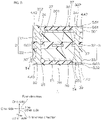
- FIG. 1 One embodiment of the wiring circuit board of the present invention is described with reference to FIG. 1 .
- a wiring circuit board 1 has a thickness.
- the wiring circuit board 1 extends in a surface direction.
- the surface direction is orthogonal to a thickness direction.
- the wiring circuit board 1 has an appropriately flat board shape.
- the wiring circuit board 1 includes a porous insulating layer 2 and a conductive layer 3 sequentially in the thickness direction.
- the porous insulating layer 2 includes a first porous insulating layer 21 and a second porous insulating layer 22 sequentially in the thickness direction.
- the conductive layer 3 includes a first conductive layer 31, a second conductive layer 32, and a third conductive layer 33 sequentially in the thickness direction.
- the wiring circuit board 1 includes the third conductive layer 33, the second porous insulating layer 22, the second conductive layer 32, the first porous insulating layer 21, and the first conductive layer 31 toward one side in the thickness direction.
- the wiring circuit board 1 further includes a conductor connecting portion 4, an insulating cover layer 5, and an adhesive layer 6.
- the porous insulating layer 2 includes the first porous insulating layer 21 and the second porous insulating layer 22 toward the other side in the thickness direction.
- the first porous insulating layer 21 has a thickness.
- the first porous insulating layer 21 extends in the surface direction.
- the first porous insulating layer 21 has an appropriately flat board shape.
- the first porous insulating layer 21 includes a first penetrating hole 23 and two second penetrating holes 24.
- the first penetrating hole 23 is disposed at an intermediate portion of the first porous insulating layer 21 in a first direction.
- the first direction is included in the surface direction.
- One of the second penetrating holes 24 is disposed at one side of the first penetrating hole 23 in the first direction, holding an interval therebetween.
- the other second penetrating hole 24 is disposed at the other side of the first penetrating hole 23 in the first direction, holding an interval therebetween.
- the other second penetrating hole 24 is disposed across the first penetrating hole 23 from the one second penetrating hole 24 in the first direction. In this manner, the one second penetrating hole 24, the first penetrating hole 23, and the other second penetrating hole 24 are arranged sequentially in the first direction. In other words, the first penetrating hole 23 is disposed between the two second penetrating holes 24.
- Inner peripheral surfaces of the first porous insulating layer 21 go along the thickness direction and define the first penetrating hole 23 and the two second penetrating holes 24, respectively.
- the inner peripheral surfaces each may have a tapered shape having a cross-sectional area gradually increasing toward one side in the thickness direction.
- the second porous insulating layer 22 is disposed at the other side of the first porous insulating layer 21 in the thickness direction.
- the second porous insulating layer 22 is separated from the first porous insulating layer 21 by an interval in the thickness direction.
- the second porous insulating layer 22 is bonded to the first porous insulating layer 21 through a second adhesive layer 62 that is described below.
- the second porous insulating layer 22 has a thickness.
- the second porous insulating layer 22 extends in the surface direction.
- the second porous insulating layer 22 has an appropriately flat board shape.
- the second porous insulating layer 22 has two third penetrating holes 25.
- the two third penetrating holes 25 overlap the two second penetrating holes 24, respectively.
- the two third penetrating holes 25 are next to each other in the first direction, holding an interval therebetween.
- the two third penetrating holes 25 penetrate the second porous insulating layer 22 in the thickness direction.
- Inner peripheral surfaces of the second porous insulating layer 22 go along the thickness direction and define the two third penetrating holes 25, respectively.
- the inner peripheral surfaces each may have a tapered shape having a cross-sectional area gradually increasing toward the other side in the thickness direction.
- Examples of the material of the porous insulating layer 2 include resin.
- the resin is not especially limited.
- Examples of the resin include polycarbonate resin, polyimide resin, polyimide fluoride resin, epoxy resin, phenol resin, urea resin, melamine resin, diallyl phthalate resin, silicone resin, thermosetting urethane resin, fluorine resin, and a liquid crystal polymer.
- a polyimide resin and a liquid crystal polymer are used.
- the porous insulating layer 2 is porous.
- the porous insulating layer 2 has a closed cell and/or an opened cell.
- the porous insulating layer 2 has a porosity of, for example, 50% or more, preferably 60% or more, more preferably 70% or more, even more preferably 80% or more.
- the porous insulating layer 2 has a porosity of, for example, less than 100%, and 99% or less.
- the porous insulating layer 2 has a permittivity of, for example, 2.5 or less, preferably 1.9 or less, more preferably 1.6 or less, and, for example, more than 1.0 at a frequency of 60 GHz.
- the permittivity of the porous insulating layer 2 is measured by a resonator method using a frequency of 60 GHz.
- the dielectric loss tangent of the porous insulating layer 2 at a frequency of 60 GHz is, for example, 0.006 or less, and, for example, more than 0.
- the dielectric loss tangent of the porous insulating layer 2 is measured by a resonator method using a frequency of 60 GHz.
- the conductive layer 3 extends in a second direction.
- the second direction intersects with the thickness direction and the first direction. Specifically, the second direction is orthogonal to the thickness direction and the first direction.
- the conductive layer 3 includes the first conductive layer 31, the second conductive layer 32, and the third conductive layer 33 sequentially toward the other side in the thickness direction.
- the first conductive layer 31 is disposed at one side in the thickness direction of the first porous insulating layer 21. Specifically, the first conductive layer 31 is disposed on one surface in the thickness direction of the first porous insulating layer 21.
- the first conductive layer 31 has a first signal wire 34 which exemplifies a first wiring portion and two first ground wires 35 which exemplify two second wiring portions.
- the first signal wire 34 transmits a signal in the second direction.
- Examples of the signal include differential signals.
- the signal includes a low current of, for example, less than 1A, and less than 0.1A.
- the first signal wire 34 is disposed at an intermediate portion of the first conductive layer 31 in the first direction.
- the first signal wire 34 is disposed at one side in the thickness direction of the first penetrating hole 23.
- the first signal wire 34 closes one end in the thickness direction of the first penetrating hole 23.
- the first signal wire 34 is in contact with one surface in the thickness direction of the first porous insulating layer 21 around the first penetrating hole 23.
- the first signal wire 34 includes a signal terminal 341.
- the signal terminal 341 is disposed at an end in the second direction of the first signal wire 34.
- the signal terminal 341 is connected to an electrode of an outer board not illustrated.
- the first signal wire 34 is thinner than each of the first ground wires 35 described next.
- the first signal wire 34 has a thickness T1 of, for example, 50 ⁇ m or less, preferably 35 ⁇ m or less, more preferably 18 ⁇ m or less, and, for example, 4 ⁇ m or more.
- the thickness T1 of the first signal wire 34 is a thickness-direction length between one surface in the thickness direction of the first porous insulating layer 21 and one surface in the thickness direction of the first signal wire 34.
- Each of the two first ground wires 35 makes an electrical connection with the earth to return a faint current that affects the first signal wire 34 back to the ground.
- the faint current includes a current of, for example, less than 1A, and less than 0.1A.
- the two first ground wires 35 are disposed at one side in the thickness direction of the two second penetrating holes 24, respectively.
- the two first ground wires 35 close one ends in the thickness direction of the two second penetrating holes 24, respectively.
- Each of the two first ground wires 35 is in contact with the one surface in the thickness direction of the first porous insulating layer 21 around each of the two second penetrating holes 24.
- the two first ground wires 35 are separated from each other by an interval in the first direction.
- One of the first ground wires 35 is disposed at one side of the first signal wire 34 in the first direction, holding an interval therebetween.
- the other first ground wire 35 is disposed at the other side of the first signal wire 34 in the first direction, holding an interval therebetween.
- the other first ground wire 35 is disposed across the first signal wire 34 from the one first ground wire 35 in the first direction. In this manner, the one first ground wire 35, the first signal wire 34, and the other first ground wires 35 are arranged in the first direction, holding an interval therebetween.
- the first signal wire 34 is disposed between the two first ground wires 35.
- At least one of the two first ground wires 35 includes a ground terminal 351.
- the ground terminal 351 is disposed at an end in the second direction of the first ground wire 35.
- the ground terminal 351 is connected to an earth member not illustrated.
- Each of the two first ground wires 35 is thicker than the first signal wire 34.
- the press described blow drastically changes the thickness of the porous insulating layer 2 that overlaps the first signal wire 34 and the first ground wires 35 in the thickness direction, and thus drastically changes the electric properties of the first signal wire 34. Specifically, this causes a mismatch in the characteristic impedance of the first signal wire 34.
- the two first ground wires 35 each have a thickness T2 of, for example, 6 ⁇ m or more, preferably 20 ⁇ m or more, more preferably 40 ⁇ m or more, and, for example, 52 ⁇ m or less.
- the thickness T2 of the first ground wire 35 is a thickness-direction between one surface in the thickness direction of the first porous insulating layer 21 and one surface in the thickness direction of the first ground wire 35.
- a ratio (T2/T1) of the thickness T2 of the first ground wire 35 to the thickness T1 of the first signal wire 34 is more than 1, preferably 1.2 or more, more preferably 1.4 or more, even more preferably 1.6 or more.
- the upper limit of the ratio (T2/T1) of the thickness T2 of the first ground wire 35 to the thickness T1 of the first signal wire 34 is not limited.
- the upper limit of the ratio (T2/T1) is, for example, 13.
- the second conductive layer 32 is disposed at the other side in the thickness direction of the first porous insulating layer 21.
- the second conductive layer 32 is disposed across the first porous insulating layer 21 from the first conductive layer 31 in the thickness direction.
- the second conductive layer 32 is disposed between the first porous insulating layer 21 and the second porous insulating layer 22 the thickness direction.
- the second conductive layer 32 is electrically connected to the first conductive layer 31.
- the second conductive layer 32 includes a second signal wire 36 and two second ground wires 37.
- the second signal wire 36 transmits the above-described signal, working together with the first signal wire 34 in the second direction. When being projected in the thickness direction, the second signal wire 36 overlaps the first signal wire 34. The second signal wire 36 is electrically connected to the first signal wire 34 in the thickness direction.
- the two second ground wires 37 make an electrical connection with the earth to return a faint current that affects the first signal wire 34 and the second signal wire 36 back to the ground, working together with the two first ground wires 35.
- the two second ground wires 37 are disposed at one side and the other side in the first direction of the second signal wire 36, holding an interval therebetween. When being projected in the thickness direction, the second ground wire 37 overlaps the first ground wire 35.
- Each of the two second ground wires 37 is the same as the second signal wire 36 in thickness.
- the third conductive layer 33 is an example of a ground layer.
- the third conductive layer 33 makes an electrical connection with the earth to return a faint current that affects the first signal wire 34 and the second signal wire 36 back to the ground, working together with the first ground wire 35 and the second ground wire 37.
- the third conductive layer 33 is disposed at the other side in the thickness direction of the second porous insulating layer 22. Specifically, the third conductive layer 33 is disposed on the other surface in the thickness direction of the second porous insulating layer 22. The third conductive layer 33 is disposed across the second porous insulating layer 22 from the second conductive layer 32 in the thickness direction.
- the third conductive layer 33 has a third ground portion 38 that exemplifies the third wiring portion and a fourth ground portion 39 that exemplifies the fourth wiring portion.
- the third ground portion 38 is disposed on the other surface in the thickness direction of the second porous insulating layer 22 between the two third penetrating holes 25.
- the third ground portion 38 extends in the first direction.
- the third ground portion 38 overlaps the first signal wire 34.
- the third ground portion 38 includes the first signal wire 34.
- the third ground portion 38 includes an overlap portion 381 and a non-overlap portion 382.
- the overlap portion 381 overlaps the first signal wire 34.
- the non-overlap portion 382 does not overlap the first signal wire 34.
- the overlap portion 381 is an intermediate portion in the first direction of the third ground portion 38.
- the non-overlap portions 382 extend outward from one end and the other end in the first direction of the overlap portion 381, respectively.
- the third ground portion 38 has a flat board shape.
- the third ground portion 38 is thinner than the fourth ground portion 39 described next.
- the third ground portion 38 has a thickness T3 of, for example, 50 ⁇ m or less, preferably 35 ⁇ m or less, more preferably 18 ⁇ m or less, and, for example, 4 ⁇ m or more.
- the thickness T3 of the third ground portion 38 is a thickness-direction length between the other surface in the thickness direction of the second porous insulating layer 22 and the other surface in the thickness direction of the third ground portion 38.
- the two fourth ground portions 39 are disposed at the other side in the thickness direction of the two third penetrating holes 25, respectively.
- the two fourth ground portions 39 close the other ends in the thickness direction of the two third penetrating holes 25, respectively.
- Each of the two fourth ground portions 39 is in contact with the other surface in the thickness direction of the second porous insulating layer 22 around each of the two third penetrating holes 25.
- the two fourth ground portions 39 are separated by an interval in the first direction.
- Each of the two fourth ground portions 39 has a flat board shape.
- the fourth ground portions 39 overlap the first ground wires 35.
- a one-side part in the thickness direction of one of the fourth ground portions 39 is coupled to one end in the first direction of the third ground portion 38 (non-overlap portion 382).
- a one-side part in the thickness direction of the other fourth ground portion 39 is coupled to the other end in the first direction of the third ground portion 38 (overlap portion 382). In this manner, the two fourth ground portions 39 are electrically connected to each other via the third ground portion 38.
- Each of the two fourth ground portions 39 is thicker than the third ground portion 38.
- Each of the two fourth ground portions 39 thicker than the third ground portion 38 can suppress a drastic change in the thickness of the porous insulating layer 2, which overlaps the third ground portion 38 and the fourth ground portions 39 in the thickness direction, by the press described below, and consequently can suppress a drastic change in the electric properties of the first signal wire 34 and second signal wire 36.
- Each of the two fourth ground portions 39 has a thickness T4 of, for example, 6 ⁇ m or more, preferably 20 ⁇ m or more, more preferably 40 ⁇ m or more, and, for example, 52 ⁇ m or less.
- the thickness T4 of the fourth ground portion 39 is a thickness-direction between the other surface in the thickness direction of the second porous insulating layer 22 and the other surface in the thickness direction of the fourth ground portion 39.
- a ratio (T4/T3) of the thickness T4 of the fourth ground portion 39 to the thickness T3 of the third ground portion 38 is more than 1, preferably 1.2 or more, more preferably 1.4 or more, even more preferably 1.6 or more.
- the upper limit of the ratio (T4/T3) of the thickness T4 of the fourth ground portion 39 to the thickness T3 of the third ground portion 38 is not limited.
- the upper limit of the ratio (T4/T3) is, for example, 13.
- the material of the conductive layer 3 is not limited.
- Examples of the material of the conductive layer 3 include copper, iron, silver, gold, aluminum, nickel, and alloys thereof (stainless steels and bronze).
- Preferably copper is used as the material of the conductive layer 3.
- the conductor connecting portion 4 is disposed between the first conductive layer 31 and the second conductive layer 32 and between the second conductive layer 32 and the third conductive layer 33 in the thickness direction.
- the conductor connecting portion 4 is disposed in the first penetrating hole 23, the second penetrating holes 24, and the third penetrating holes 25.
- the conductor connecting portion 4 has a first conductor connecting portion 41, two second conductor connecting portions 42, and two third conductor connecting portions 43.
- a part (major part) of the first conductor connecting portion 41 fills the first penetrating hole 23, and the remaining part (the other end in the thickness direction) of the first conductor connecting portion 41 protrudes from the first penetrating hole 23 toward the other side in the thickness direction.
- One end in the thickness direction of the first conductor connecting portion 41 is in contact with (continues to) the first signal wire 34.
- the other end in the thickness direction of the first conductor connecting portion 41 is in contact with the second signal wire 36.
- the first signal wire 34 and the second signal wire 36 are electrically connected to each other via the first conductor connecting portion 41. Consequently, the first signal wire 34, the second signal wire 36, and the first conductor connecting portion 41 form an approximately I-shaped signal path in the cross-sectional view.
- the signal path extends in the thickness direction and the second direction.
- a part (major part) of each of the second conductor connecting portions 42 fills each of the second penetrating holes 24, and the remaining part (the other end in the thickness direction) of each of the second conductor connecting portions 42 protrudes from the second penetrating hole 24 toward the other side in the thickness direction.
- One end in the thickness direction of each of the second conductor connecting portions 42 is in contact with (continues to) each of the first ground wires 35.
- the other end in the thickness direction of each of the second conductor connecting portions 42 is contact with each of the second ground wires 37. In this manner, the first ground wires 35 and the second ground wires 37 are electrically connected to each other via the second conductor connecting portions 42.
- a part (major part) of each of the third conductor connecting portions 43 fills each of the third penetrating holes 25, the remaining part (one end in the thickness direction) of each of the third conductor connecting portions 43 protrudes from each of the third penetrating holes 25 toward one side in the thickness direction.
- the other end in the thickness direction of each of the third conductor connecting portions 43 is in contact with (continues to) each of the fourth ground portions 39.
- One end in the thickness direction of each of the third conductor connecting portions 43 is in contact with each of the second ground wires 37. In this manner, the second ground wires 37 and the third conductive layer 33 are electrically connected to each other via the third conductor connecting portions 43.
- the first ground wires 35, the second ground wires 37, the third conductive layer 33, the second conductor connecting portions 42, and the third conductor connecting portions 43 form an approximately U-shaped ground path in the cross-sectional view.
- the ground path opens toward one side in the thickness direction in the cross-sectional view.
- the material of the conductor connecting portion 4 is the same as the above-described material of the conductive layer 3.
- the insulating cover layer 5 is disposed at one side and the other side in the thickness direction of the conductive layer 3.
- the insulating cover layer 5 has a first insulating cover layer 51 and a second insulating cover layer 52.
- the first insulating cover layer 51 is disposed at one side of the first conductive layer 31 in the thickness direction.
- the first insulating cover layer 51 forms one surface in the thickness direction of the wiring circuit board 1.
- the first insulating cover layer 51 exposes the signal terminal 341 and the ground terminal 351.
- the first insulating cover layer 51 covers the first conductive layer 31 other than the signal terminal 341 and the ground terminal 351.
- the second insulating cover layer 52 is disposed at the other side of the third conductive layer 33 in the thickness direction.
- the second insulating cover layer 52 forms the other surface in the thickness direction of the wiring circuit board 1.
- the second insulating cover layer 52 covers the third conductive layer 33.
- Examples of the material of the insulating cover layer 5 include the resins cited above.
- the adhesive layer 6 is disposed between the above-described layers.
- the material (or raw material) of the adhesive layer 6 is not limited.
- the adhesive layer 6 includes a first adhesive layer 61, a second adhesive layer 62, and a third adhesive layer 63 toward the other side in the thickness direction.
- the first adhesive layer 61 is disposed at one surfaces in the thickness direction of the first conductive layer 31 and first porous insulating layer 21, and the other surface in the thickness direction of the first insulating cover layer 51.
- the first adhesive layer 61 bonds the first conductive layer 31 and first porous insulating layer 21 to the first insulating cover layer 51.
- the first adhesive layer 61 is in contact with one surfaces and side surfaces in the thickness direction of the first conductive layer 31, and one surface in the thickness direction of the first porous insulating layer 21 around the first conductive layer 31.
- the first adhesive layer 61 is in contact with the other surface in the thickness direction of the first insulating cover layer 51.
- the second adhesive layer 62 is disposed at the other surface in the thickness direction of the first porous insulating layer 21 and one surface in the thickness direction of the second porous insulating layer 22. In other words, the second adhesive layer 62 is disposed between the first porous insulating layer 21 and the second porous insulating layer 22.
- the second adhesive layer 62 embeds the second conductive layer 32 in the thickness direction. Specifically, the second adhesive layer 62 is in contact with both surfaces in the thickness direction of the second conductive layer 32 and side surfaces in the thickness direction of the second conductive layer 32.
- the second adhesive layer 62 is in contact with the side surfaces of the above-described remaining parts of the conductor connecting portion 4.
- the second adhesive layer 62 is in contact with a peripheral side surface of the other end in the thickness direction of the first conductor connecting portion 41, a peripheral side surface of the other end in the thickness direction of the second conductor connecting portion 42, and a peripheral side surface of one end in the thickness direction of the third conductor connecting portion 43.
- the third adhesive layer 63 is disposed on the other surface in the thickness direction of the third conductive layer 33, the other surface in the thickness direction of the second porous insulating layer 22, and one surface in the thickness direction of the second insulating cover layer 52.
- FIG. 1 does not illustrate a mode in which the third adhesive layer 63 is disposed on the other surface in the thickness direction of the second porous insulating layer 22.
- the third adhesive layer 63 bonds the third conductive layer 33 and second porous insulating layer 22 to the second insulating cover layer 52.
- the third adhesive layer 63 is in contact with the other surface in the thickness direction of the third conductive layer 33 and side surfaces in the thickness direction of the third conductive layer 33, and the other surface in the thickness direction of the second porous insulating layer 22 around the third conductive layer 33.
- the wiring circuit board 1 may include a fourth adhesive layer 64 and a reinforcement layer 7, both of which are illustrated by the phantom lines.
- the fourth adhesive layer 64 is disposed on the other surface in the thickness direction of the second insulating cover layer 52.
- the fourth adhesive layer 64 bonds the second insulating cover layer 52 to the reinforcement layer 7 described next.
- the reinforcement layer 7 reinforces the first signal wire 34 and the third ground portion 38.
- the reinforcement layer 7 is disposed at the other side in the thickness direction of the second insulating cover layer 52. Specifically, the reinforcement layer 7 is bonded to the other surface in the thickness direction of the second insulating cover layer 52 via the fourth adhesive layer 64. When being projected in the thickness direction, the reinforcement layer 7 overlaps the first signal wire 34 and the third ground portion 38.
- the reinforcement layer 7 has a flat board shape.
- the material of the reinforcement layer 7 is not limited. Examples of the material of the reinforcement layer 7 include metals and hard resins. Preferable examples of the material of the reinforcement layer 7 include metals, specifically, stainless-steel, copper, iron, and aluminum.
- the thickness of the reinforcement layer 7 is not limited.
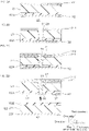
- a first porous laminate 81 is prepared first in the method.
- the first porous laminate 81 includes a second conductive layer 32, a one-side second adhesive layer 62A, the first porous insulating layer 21, and a first underlying layer 311 toward one side in the thickness direction.
- the second conductive layer 32 is disposed at the other side in the thickness direction of the first porous insulating layer 21 in the first porous laminate 81.
- the second conductive layer 32 of the first porous laminate 81 is yet to be patterned, and is not the second conductive layer 32 of the wiring circuit board 1 illustrated in FIG. 1 .
- the one-side second adhesive layer 62A is disposed on one surface in the thickness direction of the second conductive layer 32 and the other surface in the thickness direction of the first porous insulating layer 21.
- the first underlying layer 311 is disposed on one surface in the thickness direction of the first porous insulating layer 21.
- the first underlying layer 311 is included in the first conductive layer 31 of the wiring circuit board 1 illustrated in FIG. 1 .
- a method of preparing the first porous laminate 81 is described in, for example, Japanese Unexamined Patent Publication No. 2019-123851 .
- a first via 91 is formed in the first underlying layer 311, the first porous insulating layer 21, and the one-side second adhesive layer 62A.
- the first via 91 formed in the first porous insulating layer 21 is the above-described first penetrating hole 23.
- Examples of a method of forming the first via 91 include a piercing process.
- Examples of the piercing process include a laser process, a drilling process, and a blasting method.
- a laser process is used.
- the first plated layer 312 is formed on an inner peripheral surface of the first via 91 and one surface in the thickness direction of the first underlying layer 311.
- the first plated layer 312 formed on the inner peripheral surface of the first via 91 is the above-described first conductor connecting portion 41.
- the second conductive layer 32 is patterned to form the second signal wire 36 and the two second ground wires 37.
- Examples of the patterning of the second conductive layer 32 include wet etching and dry etching. Preferably wet etching is used.
- the second porous laminate 82 is bonded to the second conductive layer 32.
- the second porous laminate 82 is prepared first.
- the second porous laminate 82 includes the other-side second adhesive layer 62B, the second porous insulating layer 22, and a second underlying layer 331 sequentially toward the other side in the thickness direction.
- the other-side second adhesive layer 62B is disposed on one surface in the thickness direction of the second porous insulating layer 22.
- the second underlying layer 331 is disposed on the other surface in the thickness direction of the second porous insulating layer 22.
- the second underlying layer 331 is included in the third conductive layer 33.
- a method of preparing the second porous laminate 82 is described in, for example, Japanese Unexamined Patent Publication No. 2019-123851.
- the other-side second adhesive layer 62B of the second porous laminate 82 is bonded to the second conductive layer 32.
- a press machine (not illustrated) that can carry out the press in the thickness direction is used.
- the pressure of the press is not limited.
- the pressure of the press is, for example, 0.5 MPa or more, preferably 3 MPa or more, and, for example, 10 MPa or less.
- the press is carried out for a time of, for example, 1 minute or more, preferably 10 minutes or more, and, for example, 120 minutes or less.
- the press may be a hot press.
- the press is carried out at a temperature of, for example, 80°C or more, preferably 120°C or more, and, for example, 300°C or less.
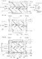
- the one-side second adhesive layer 62A and the other-side second adhesive layer 62B are deformed and enter between the adjacent second signal wire 36 and second ground wires 37. In this manner, the one-side second adhesive layer 62A and the other-side second adhesive layer 62B form the second adhesive layer 62.
- the phantom lines of FIG. 3A to FIG. 4B each illustrate the boundary between the one-side second adhesive layer 62A and the other-side second adhesive layer 62B. However, the boundary may not be observed.
- the one-side second adhesive layer 62A and the other-side second adhesive layer 62B are integrated.
- a second via 92 is formed in the first plated layer 312, the first underlying layer 311, and the one-side second adhesive layer 62A.
- the second vias 92 formed in the first porous insulating layer 21 are the second penetrating holes 24.
- a third via 93 is formed in the second underlying layer 331, the second porous insulating layer 22, and the other-side second adhesive layer 62B.
- the third vias 93 formed in the second porous insulating layer 22 are the third penetrating holes 25.
- Examples of a method of forming the second vias 92 and the third vias 93 include the method cited as the method of forming the first via 91.
- a second plated layer 313 is formed on one surface in the thickness direction of the first plated layer 312 and an inner peripheral surface of the second via 92.
- a third plated layer 332 is formed on the other surface in the thickness direction of the second underlying layer 331 and an inner peripheral surface of the third via 93.
- a first resist 95 and a second resist 96 are disposed on one surface in the thickness direction of the first plated layer 312 and the other surface in the thickness direction of the second underlying layer 331, respectively.
- the first resist 95 and the second resist 96 are resists for plating.
- the first resist 95 has a reverse pattern of the second plated layer 313.
- the second resist 96 has a reverse pattern of the third plated layer 332.
- a plating process is carried out by immersing a resist laminate 83 including the first plated layer 312 and the second underlying layer 331 in a plating bath, while the first resist 95 is disposed on the first plated layer 312 and the second resist 96 is disposed on the second underlying layer 331.
- the second plated layer 313 is deposited on one surface in the thickness direction of the first plated layer 312 that is exposed from the first resist 95, and on the inner peripheral surface of the second via 92. On the other hand, the second plated layer 313 is not deposited on one surface in the thickness direction of the first plated layer 312 on which the first resist 95 is disposed.
- the third plated layer 332 is deposited on the other surface in the thickness direction of the second underlying layer 331 that is exposed from the second resist 96, and on the inner peripheral surface of the third via 93. On the other hand, the third plated layer 332 is not deposited on the other surface in the thickness direction of the second underlying layer 331 on which the second resist 96 is disposed.
- the third conductive layer 33 including the third ground portion 38 and the fourth ground portions 39 is formed.
- the third ground portion 38 is formed from the second underlying layer 331.
- the thickness T3 of the third ground portion 38 is the same as that of the second underlying layer 331.
- the fourth ground portion 39 is formed from the second underlying layer 331 and the third plated layer 332.
- the thickness T4 of each of the fourth ground portions 39 is the same as the total thickness of the second underlying layer 331 and the third plated layer 332.
- the first plated layer 312 and the first underlying layer 311 are patterned.
- Examples of the patterning of the first plated layer 312 and the first underlying layer 311 include wet etching and dry etching. Preferably, wet etching is used. In this manner, the first conductive layer 31 including the first signal wire 34 and the first ground wire 35 is formed (implementation of the first step).
- the first signal wire 34 is formed from the patterned first underlying layer 311 and the patterned first plated layer 312.
- the thickness T1 of the first signal wire 34 is the total thickness of the first underlying layer 311 and the first plated layer 312.
- the first ground wire 35 is formed from the patterned first underlying layer 311, the patterned first plated layer 312, and the patterned second plated layer 313.
- the thickness T2 of the first ground wire 35 is the total thickness of the first underlying layer 311, the first plated layer 312, and the second plated layer 313.
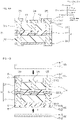
- a first cover laminate 85 is bonded to the first conductive layer 31 (implementation of the second step).
- the first cover laminate 85 includes the first insulating cover layer 51 and the first adhesive layer 61 sequentially toward the other side in the thickness direction.
- a second cover laminate 86 is bonded to the third conductive layer 63.
- the second cover laminate 86 includes the second insulating cover layer 52 and the third adhesive layer 63 sequentially toward one side in the thickness direction.
- the above-described press machine is used for the bonding.
- the conditions for the press are the same as described above.
- the first adhesive layer 61 enters between the adjacent first signal wire 34 and first ground wires 35.
- the first adhesive layer 61 is in contact with one surface in the thickness direction of the first porous insulating layer 21 exposed from the first signal wire 34 and the first ground wire 35.
- the second adhesive layer 62 is brought into contact with the other surface in the thickness direction of the second porous insulating layer 22 around the third conductive layer 33.
- the wiring circuit board 1 which includes the porous insulating layer 2, the conductive layer 3, the conductor connecting portion 4, the insulating cover layer 5, and the adhesive layer 6, is produced.
- the reinforcement layer 7 is bonded to the second insulating cover layer 52 via the fourth adhesive layer 64.
- the above-described press machine is used for the bonding of the reinforcement layer 7.
- the conditions for the press are the same as describe above.
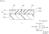
- the wiring circuit board 1 includes the first ground wires 35 each thicker than the first signal wire 34. In other words, the first signal wire 34 is thinner than each of the first ground wires 35.
- the pressing of the first porous insulating layer 21 in the thickness direction applies a lower pressure on the first porous insulating layer 21 that overlaps the first signal wire 34 in the thickness direction than on the first porous insulating layer 21 that overlaps the first ground wires 35 in the thickness direction.
- the change in the thickness of the first porous insulating layer 21 that overlaps the first signal wire 34 in the thickness direction is suppressed more than the change in the thickness of the first porous insulating layer 21 that overlaps the first ground wires (second wiring portions) 35 in the thickness direction.
- the mismatch in the characteristic impedance of the first signal wire 34 can be suppressed.
- the change in the electric properties of the first signal wire 34 is suppressed more than the change in the electric properties of the first ground wires 35.
- the first porous insulating layer 21 that overlaps the first ground wires 35 drastically changes.
- the faint current flowing through the first ground wire 35 is returned back to the ground by the electrical connection with the earth. This allows a large change in the electric properties of the first ground wires 35.
- the third conductive layer 33 which is a ground layer, includes the third ground portion 38, which overlaps the first signal wire 34, and the fourth ground portion 39, which overlaps the first ground wire 35 and is thicker than the third ground portion 38.
- the porous insulating layer 2 (the first porous insulating layer 21 and second porous insulating layer 22) that overlaps the first signal wire 34 in the thickness direction receives a lower pressure than the porous insulating layer 2 that overlaps the first ground wires 35 in the thickness direction does.
- the change in the thickness of the porous insulating layer 2 that overlaps the first signal wire 34 in the thickness direction is suppressed more than the change in the thickness of the porous insulating layer 2 that overlaps the first ground wires 35 in the thickness direction as described above.
- the change in the electric properties of the first signal wire 34 can be suppressed more than the change in the electric properties of the first ground wires 35.
- the first ground wire 35, the second ground wire 37, and the third conductive layer 33 may be a first power wire, a second power wire, and a power layer, respectively.
- the first power wire, the second power wire, and the power layer form a power path together with the second conductor connecting portion 42 and the third conductor connecting portion 43.
- a large current for example, 1A or more or 10A or more flows through the power path.
- the first signal wire 34 is disposed between the two first ground wires 35.
- a variation may include a first signal wire 34 disposed across one of the first ground wires 35 from the other first ground wire 35 in the first direction.
- the first signal wire 34 may be disposed across the other first ground wire 35 from the one first ground wire 35 in the first direction.
- the first signal wire 34 is disposed between the two first ground wires 35.
- the porous insulating layer 2 that overlaps the two first ground wires 35 in the thickness direction can receive the high pressure while keeping the balance between the pressures on the two overlapping parts during the press using a flat board-shaped pressing plate.
- the porous insulating layer 2 that overlaps the first signal wire 34 disposed between the two first ground wires 35 receives a lower pressure. This can suppress the change in the thickness of the porous insulating layer 2 that overlaps the first signal wire 34 in the thickness direction more than the change in the thickness of the porous insulating layer 2 that overlaps the first ground wires 35 in the thickness direction.
- one first ground wire (second wiring portion) 35 may be provided.
- the conductive layer 3 has a first conductive layer 30 that exemplifies a ground layer.
- the first conductive layer 30 is disposed on one surface in the thickness direction of the first porous insulating layer 21.
- the first conductive layer 30 includes a first ground portion 301 and a second ground portion 302.
- the first ground portion 301 is disposed on one surface in the thickness direction of the first porous insulating layer 21 between the two second penetrating holes 24.
- the first ground portion 301 extends in the first direction. When being projected in the thickness direction, the first ground portion 301 overlaps the third ground portion 38.
- the first ground portion 301 has a flat board shape.
- the other-side part in the thickness direction of one of the second ground portions 302 is coupled to one end in the first direction of the first ground portion 301.
- the other-side part in the thickness direction of the other second ground portion 302 is coupled to the other end in the first direction of the first ground portion 301. In this manner, the two second ground portions 302 are electrically connected to each other via the first ground portion 301.
- the first conductive layer 30, the second ground wires 37, the third conductive layer 33, and the conductor connecting portion 4 form a ground path having an approximately rectangular frame shape in the cross-sectional view.
- the rectangular frame surrounds the second signal wire 36 in the cross-sectional view.
- the wiring circuit board 1 includes one porous insulating layer 2, one conductive layer 3, two adhesive layers 6, and one insulating cover layer 5.
- the porous insulating layer 2 is the first porous insulating layer 21.
- the first porous insulating layer 21 does not include the second penetrating holes 24.
- the conductive layer 3 is the first conductive layer 31.
- the adhesive layers 6 include the first adhesive layer 61 and the second adhesive layer 62.
- the insulating cover layer 5 is the first insulating cover layer 51.
- the first porous insulating layer 21, the second adhesive layer 62, the first conductive layer 31, the first adhesive layer 61, and the first insulating cover layer 51 are disposed sequentially toward one side in the thickness direction.
- the conductive layer 3 includes the first conductive layer 31 and a third conductive layer 40.
- the third conductive layer 40 includes the second signal wire 36 and the two fourth ground portions 39.
- the porous insulating layer 2 includes a skin layer on one end and/or the other end in the thickness direction of the porous insulating layer 2.
- the skin layer extends in the surface direction.
- the skin layer is flat and smooth.
- the first porous insulating layer 21 includes a skin layer disposed on one end and/or the other end in the thickness direction of the first porous insulating layer 21.
- the second porous insulating layer 22 includes a skin layer on one end and/or the other end in the thickness direction of the second porous insulating layer 22.
- the skin layer located on one end of the first porous insulating layer 21 in the thickness direction forms one surface of the first porous insulating layer 21 in the thickness direction.
- the skin layer located on the other end of the first porous insulating layer 21 in the thickness direction forms the other surface of the first porous insulating layer 21 in the thickness direction.
- a ratio of the thickness of each of the skin layers to the thickness of the first porous insulating layer 21 is, for example, less than 0.1.
- the thickness of each of the skin layers is appropriately adjusted to ensure the peel strength of the skin layer from the first underlying layer 311.
- the skin layers each have a thickness, for example, 1 ⁇ m or more, and, for example, 50 ⁇ m or less, preferably, 30 ⁇ m or less.
- the skin layer located on one end of the second porous insulating layer 22 in the thickness direction forms one surface of the second porous insulating layer 22 in the thickness direction.
- the skin layer located on the other end of the second porous insulating layer 22 in the thickness direction forms the other surface of the second porous insulating layer 22 in the thickness direction.
- a ratio of the thickness of each of the skin layers to the thickness of the second porous insulating layer 22 is, for example, less than 0.1.
- the thickness of each of the skin layers is appropriately adjusted to ensure the peel strength of the skin layer from the other-side second adhesive layer 62B.
- the skin layers each have a thickness of, for example, 1 ⁇ m or more, and, for example, 50 ⁇ m or less, preferably, 30 ⁇ m or less.
- the adhesive layer 6 includes a fourth adhesive layer and a fifth adhesive layer, both of which are not illustrated.
- the fourth adhesive layer is disposed on one surface in the thickness direction of the first porous insulating layer 21.
- the fourth adhesive layer intervenes between the first porous insulating layer 21 and the first conductive layer 31.
- the fourth adhesive layer bonds the first porous insulating layer 21 to the first conductive layer 31.
- the fourth adhesive layer and the second adhesive layer 62 are disposed on one surface and the other surface in the thickness direction of the first porous insulating layer 21, respectively.
- the fifth adhesive layer is disposed on the other surface in the thickness direction of the second porous insulating layer 22.
- the fifth adhesive layer intervenes between the second porous insulating layer 22 and the third conductive layer 33.
- the fifth adhesive layer bonds the second porous insulating layer 22 to the third conductive layer 33.
- the second adhesive layer 62 (the other-side second adhesive layer 62B, see FIG. 3C ) and the fifth adhesive layer are disposed on one surface and the other surface in the thickness direction of the second porous insulating layer 22, respectively.
- a first porous laminate 81 which includes a second conductive layer 32, a one-side second adhesive layer 62A, a first porous insulating layer 21, a fourth adhesive layer not illustrated, and a first underlying layer 311 sequentially toward one side in the thickness direction as illustrated in FIG. 2A , is prepared.
- a second porous laminate 82 which includes the other-side second adhesive layer 62B, a second porous insulating layer 22, a fifth adhesive layer not illustrated, and a second underlying layer 331 sequentially toward the other side in the thickness direction as illustrated in the lower part of FIG. 2D , is used.
Landscapes
- Engineering & Computer Science (AREA)
- Microelectronics & Electronic Packaging (AREA)
- Manufacturing & Machinery (AREA)
- Physics & Mathematics (AREA)
- Electromagnetism (AREA)
- Structure Of Printed Boards (AREA)
Abstract
A wiring circuit board 1 includes a porous insulating layer 2, and a first conductive layer 31 sequentially toward one side in the thickness direction. The first conductive layer 31 includes a first signal wire 34 and first ground wires 35. Each of the first ground wires 35 is thicker than the first signal wire 34.
Description
- The present invention relates to a wiring circuit board and a method of producing the wiring circuit board.
- Wiring circuit boards each including a conductive layer and a wiring circuit board are known (for example, see
Patent document 1 below). The wiring circuit board described inPatent document 1 includes a conductive layer having a plurality of wires. The wire portions ofPatent document 1 are the same in thickness. - Patent Document 1:
Japanese Unexamined Patent Publication No. 2019-123851 - The wiring circuit board may be pressed in a thickness direction depending on the use and purpose. In such a case, the press uniformly changes the thickness of several parts of the porous insulating resin film that overlap the wire portions. Consequently, the uniform change in the thickness causes a disadvantage that the electric properties of the wires uniformly change.
- The present invention provides a wiring circuit board in which the change in the electric properties of the first wiring portion can be suppressed more than the change in the electric properties of the second wiring portion, and a method of producing the wiring circuit board.
- The present invention [1] includes a wiring circuit board comprising a porous insulating layer and a conductive layer sequentially toward one side in a thickness direction, wherein the conductive layer has a first wiring portion and a second wiring portion thicker than the first wiring portion.
- The wiring circuit board includes the second wiring portion thicker than the first wiring portion. In other words, the first wiring portion is thinner than the second wiring portion.
- Thus, when the wiring circuit board is pressed in the thickness direction, the porous insulating layer overlapping the first wiring portion in the thickness direction receives a lower pressure than the porous insulating layer overlapping the second wiring portion in the thickness direction does. This can suppress the change in the thickness of the porous insulating layer overlapping the first wiring portion in the thickness direction more than the change in the thickness of the porous insulating layer overlapping the second wiring portion in the thickness direction.
- As a result, the change in the electric properties of the first wiring portion can be suppressed more than the change in the electric properties of the second wiring portion.
- The present invention [2] includes the wiring circuit board in [1], wherein two of the second wiring portions are disposed and separated from each other by an interval in a direction orthogonal to the thickness direction, and the first wiring portion is disposed between the second wiring portions.
- When the wiring circuit board is pressed, the porous insulating layer that overlaps the two second wiring portions in the thickness direction can receive a high pressure while keeping the balance between the pressures on the two overlapping parts. Thus, the porous insulating layer that overlaps the first wiring portion disposed between the two second wiring portions receives a lower pressure. This can suppress the change in the thickness of the porous insulating layer overlapping the first wiring portion in the thickness direction more than the change in the thickness of the porous insulating layer overlapping each of the second wiring portions in the thickness direction.
- The present invention [3] includes the wiring circuit board described in [1] or [2], further comprising a ground layer disposed on the other surface in the thickness direction of the porous insulating layer, wherein the ground layer has a third wiring portion and a fourth wiring portion, the third wiring portion overlaps the first wiring portion and the fourth wiring portion overlaps the second wiring portion when being projected in the thickness direction, and the fourth wiring portion is thicker than the third wiring portion.
- In the wiring circuit board, the ground layer includes the third wiring portion, which overlaps the first wiring portion, and the fourth wiring portions, which overlap the second wiring portions and are thicker than the third wiring portion. Thus, when the wiring circuit board is pressed in the thickness direction, the porous insulating layer overlapping the first wiring portion in the thickness direction receives a lower pressure than the porous insulating layer overlapping each of the second wiring portions in the thickness direction does. This can suppress the change in the thickness of the porous insulating layer overlapping the first wiring portion in the thickness direction more than the change in the thickness of the porous insulating layer overlapping each of the second wiring portions in the thickness direction.
- The present invention [4] includes the wiring circuit board described in described in [3], wherein the porous insulating layer has a penetrating hole penetrating the porous insulating layer in the thickness direction, and the wiring circuit board further comprises a conductor connecting portion filling the penetrating hole and being in contact with the conductive layer and the ground layer.
- The present invention [5] includes the wiring circuit board described in described in any one of [1] to [4], further comprising: an adhesive layer; and an insulating cover layer, wherein the insulating cover layer covers the conductive layer and the porous insulating layer through the adhesive layer from one side in the thickness direction.
- The present invention [6] includes a method of producing a wiring circuit board, the method comprising: a first step of disposing a conductive layer on one surface in a thickness direction of a porous insulating layer, wherein the conductive layer includes a first wiring portion and a second wiring portion thicker than the first wiring portion; and a second step of pressing the insulating cover layer through an adhesive layer to the conductive layer and the porous insulating layer.
- Even when the insulating cover layer is pressed to the conductive layer and the porous insulating layer through the adhesive layer and a high pressure is applied on the porous insulating layer in the second step, the method of the present invention can suppress the change in the thickness of the porous insulating layer overlapping the first wiring portion in the thickness direction more than the change in the thickness of the porous insulating layer overlapping the second wiring portion in the thickness direction. As a result, the change in the electric properties of the first wiring portion can be suppressed more than the change in the electric properties of the second wiring portion.
- By using the wiring circuit board of the present invention and the method of producing the wiring circuit board, the change in the electric properties of the first wiring portion can be suppressed more than the change in the electric properties of the second wiring portion.
-
- [
FIG. 1] FIG. 1 is a cross-sectional view of one embodiment of the present invention. - [
FIG. 2] FIG. 2A to FIG. 2D illustrate the steps of producing the wiring circuit board ofFIG. 1 . -
FIG. 2A illustrates a step for preparing a first porous laminate.FIG. 2B illustrates a step for forming a first via.FIG. 2C illustrates a step for forming a first plated layer.FIG. 2D illustrates a step for patterning a second conductive layer. - [
FIG. 3 ] Subsequently toFIG. 2D ,FIG. 3A to FIG. 3C illustrate the steps of producing the wiring circuit board.FIG. 3A illustrates a step of bonding a second porous laminate to the second conductive layer.FIG. 3B illustrates a step of forming a second via and a third via. -
FIG. 3C illustrates a step of forming a second plated layer. - [
FIG. 4 ] Subsequently toFIG. 3C ,FIG. 4A and FIG. 4B illustrate the steps of producing the wiring circuit board.FIG. 4A illustrates a step of patterning a first plated layer and a first underlying layer.FIG. 4B illustrates a step of bonding the first cover laminate and the second cover laminate together. - [
FIG. 5] FIG. 5 is a cross-sectional view of a variation of the wiring circuit board. - [
FIG. 6] FIG. 6 is a cross-sectional view of a variation of the wiring circuit board. - [
FIG. 7] FIG. 7 is a cross-sectional view of a variation of the wiring circuit board. - One embodiment of the wiring circuit board of the present invention is described with reference to
FIG. 1 . - A
wiring circuit board 1 has a thickness. Thewiring circuit board 1 extends in a surface direction. The surface direction is orthogonal to a thickness direction. Thewiring circuit board 1 has an appropriately flat board shape. - The
wiring circuit board 1 includes a porous insulatinglayer 2 and aconductive layer 3 sequentially in the thickness direction. The porousinsulating layer 2 includes a first porous insulatinglayer 21 and a second porous insulatinglayer 22 sequentially in the thickness direction. Theconductive layer 3 includes a firstconductive layer 31, a secondconductive layer 32, and a thirdconductive layer 33 sequentially in the thickness direction. Specifically, thewiring circuit board 1 includes the thirdconductive layer 33, the second porous insulatinglayer 22, the secondconductive layer 32, the first porous insulatinglayer 21, and the firstconductive layer 31 toward one side in the thickness direction. Thewiring circuit board 1 further includes aconductor connecting portion 4, an insulatingcover layer 5, and anadhesive layer 6. - The porous
insulating layer 2 includes the first porous insulatinglayer 21 and the second porous insulatinglayer 22 toward the other side in the thickness direction. - The first porous insulating
layer 21 has a thickness. The first porous insulatinglayer 21 extends in the surface direction. The first porous insulatinglayer 21 has an appropriately flat board shape. The first porous insulatinglayer 21 includes a first penetratinghole 23 and two second penetrating holes 24. - The first penetrating
hole 23 is disposed at an intermediate portion of the first porous insulatinglayer 21 in a first direction. The first direction is included in the surface direction. - One of the second penetrating
holes 24 is disposed at one side of the first penetratinghole 23 in the first direction, holding an interval therebetween. The other second penetratinghole 24 is disposed at the other side of the first penetratinghole 23 in the first direction, holding an interval therebetween. The other second penetratinghole 24 is disposed across the first penetratinghole 23 from the one second penetratinghole 24 in the first direction. In this manner, the one second penetratinghole 24, the first penetratinghole 23, and the other second penetratinghole 24 are arranged sequentially in the first direction. In other words, the first penetratinghole 23 is disposed between the two second penetrating holes 24. - The first penetrating
hole 23 and the two second penetratingholes 24 penetrate the first porous insulatinglayer 21 in the thickness direction. Inner peripheral surfaces of the first porous insulatinglayer 21 go along the thickness direction and define the first penetratinghole 23 and the two second penetratingholes 24, respectively. The inner peripheral surfaces each may have a tapered shape having a cross-sectional area gradually increasing toward one side in the thickness direction. - The second porous insulating
layer 22 is disposed at the other side of the first porous insulatinglayer 21 in the thickness direction. The second porous insulatinglayer 22 is separated from the first porous insulatinglayer 21 by an interval in the thickness direction. The second porous insulatinglayer 22 is bonded to the first porous insulatinglayer 21 through a secondadhesive layer 62 that is described below. - The second porous insulating
layer 22 has a thickness. The second porous insulatinglayer 22 extends in the surface direction. The second porous insulatinglayer 22 has an appropriately flat board shape. The second porous insulatinglayer 22 has two third penetrating holes 25. - When being projected in the thickness direction, the two third penetrating
holes 25 overlap the two second penetratingholes 24, respectively. The two third penetratingholes 25 are next to each other in the first direction, holding an interval therebetween. - The two third penetrating
holes 25 penetrate the second porous insulatinglayer 22 in the thickness direction. Inner peripheral surfaces of the second porous insulatinglayer 22 go along the thickness direction and define the two third penetratingholes 25, respectively. The inner peripheral surfaces each may have a tapered shape having a cross-sectional area gradually increasing toward the other side in the thickness direction. - Examples of the material of the porous insulating
layer 2 include resin. The resin is not especially limited. Examples of the resin include polycarbonate resin, polyimide resin, polyimide fluoride resin, epoxy resin, phenol resin, urea resin, melamine resin, diallyl phthalate resin, silicone resin, thermosetting urethane resin, fluorine resin, and a liquid crystal polymer. Preferably, a polyimide resin and a liquid crystal polymer are used. - The porous
insulating layer 2 is porous. The porousinsulating layer 2 has a closed cell and/or an opened cell. - The porous
insulating layer 2 has a porosity of, for example, 50% or more, preferably 60% or more, more preferably 70% or more, even more preferably 80% or more. The porousinsulating layer 2 has a porosity of, for example, less than 100%, and 99% or less. When the material of the porous insulatinglayer 2 is a polyimide resin, the porosity of the porous insulatinglayer 2 is obtained by a calculation using the following formula.
- Here, the permittivity of the air is 1, and the permittivity of the polyimide resin is 3.5. Thus, the following formulas hold.


- The porous
insulating layer 2 has a permittivity of, for example, 2.5 or less, preferably 1.9 or less, more preferably 1.6 or less, and, for example, more than 1.0 at a frequency of 60 GHz. The permittivity of the porous insulatinglayer 2 is measured by a resonator method using a frequency of 60 GHz. - The dielectric loss tangent of the porous insulating
layer 2 at a frequency of 60 GHz is, for example, 0.006 or less, and, for example, more than 0. The dielectric loss tangent of the porous insulatinglayer 2 is measured by a resonator method using a frequency of 60 GHz. - The
conductive layer 3 extends in a second direction. The second direction intersects with the thickness direction and the first direction. Specifically, the second direction is orthogonal to the thickness direction and the first direction. - The
conductive layer 3 includes the firstconductive layer 31, the secondconductive layer 32, and the thirdconductive layer 33 sequentially toward the other side in the thickness direction. - The first
conductive layer 31 is disposed at one side in the thickness direction of the first porous insulatinglayer 21. Specifically, the firstconductive layer 31 is disposed on one surface in the thickness direction of the first porous insulatinglayer 21. The firstconductive layer 31 has afirst signal wire 34 which exemplifies a first wiring portion and twofirst ground wires 35 which exemplify two second wiring portions. - The
first signal wire 34 transmits a signal in the second direction. Examples of the signal include differential signals. The signal includes a low current of, for example, less than 1A, and less than 0.1A. Thefirst signal wire 34 is disposed at an intermediate portion of the firstconductive layer 31 in the first direction. Thefirst signal wire 34 is disposed at one side in the thickness direction of the first penetratinghole 23. Thefirst signal wire 34 closes one end in the thickness direction of the first penetratinghole 23. Thefirst signal wire 34 is in contact with one surface in the thickness direction of the first porous insulatinglayer 21 around the first penetratinghole 23. Thefirst signal wire 34 includes a signal terminal 341. The signal terminal 341 is disposed at an end in the second direction of thefirst signal wire 34. The signal terminal 341 is connected to an electrode of an outer board not illustrated. - The
first signal wire 34 is thinner than each of thefirst ground wires 35 described next. Specifically, thefirst signal wire 34 has a thickness T1 of, for example, 50 µm or less, preferably 35 µm or less, more preferably 18 µm or less, and, for example, 4 µm or more. The thickness T1 of thefirst signal wire 34 is a thickness-direction length between one surface in the thickness direction of the first porous insulatinglayer 21 and one surface in the thickness direction of thefirst signal wire 34. - 3.1.2 Two
First Ground Wires 35 - Each of the two
first ground wires 35 makes an electrical connection with the earth to return a faint current that affects thefirst signal wire 34 back to the ground. The faint current includes a current of, for example, less than 1A, and less than 0.1A. The twofirst ground wires 35 are disposed at one side in the thickness direction of the two second penetratingholes 24, respectively. The twofirst ground wires 35 close one ends in the thickness direction of the two second penetratingholes 24, respectively. Each of the twofirst ground wires 35 is in contact with the one surface in the thickness direction of the first porous insulatinglayer 21 around each of the two second penetrating holes 24. - The two
first ground wires 35 are separated from each other by an interval in the first direction. One of thefirst ground wires 35 is disposed at one side of thefirst signal wire 34 in the first direction, holding an interval therebetween. The otherfirst ground wire 35 is disposed at the other side of thefirst signal wire 34 in the first direction, holding an interval therebetween. The otherfirst ground wire 35 is disposed across thefirst signal wire 34 from the onefirst ground wire 35 in the first direction. In this manner, the onefirst ground wire 35, thefirst signal wire 34, and the otherfirst ground wires 35 are arranged in the first direction, holding an interval therebetween. In other words, thefirst signal wire 34 is disposed between the twofirst ground wires 35. - At least one of the two
first ground wires 35 includes aground terminal 351. Theground terminal 351 is disposed at an end in the second direction of thefirst ground wire 35. Theground terminal 351 is connected to an earth member not illustrated. - Each of the two
first ground wires 35 is thicker than thefirst signal wire 34. - When each of the two
first ground wires 35 has the same thickness as that of thefirst signal wire 34, the press described blow drastically changes the thickness of the porous insulatinglayer 2 that overlaps thefirst signal wire 34 and thefirst ground wires 35 in the thickness direction, and thus drastically changes the electric properties of thefirst signal wire 34. Specifically, this causes a mismatch in the characteristic impedance of thefirst signal wire 34. - The two
first ground wires 35 each have a thickness T2 of, for example, 6 µm or more, preferably 20 µm or more, more preferably 40 µm or more, and, for example, 52 µm or less. The thickness T2 of thefirst ground wire 35 is a thickness-direction between one surface in the thickness direction of the first porous insulatinglayer 21 and one surface in the thickness direction of thefirst ground wire 35. - A ratio (T2/T1) of the thickness T2 of the
first ground wire 35 to the thickness T1 of thefirst signal wire 34 is more than 1, preferably 1.2 or more, more preferably 1.4 or more, even more preferably 1.6 or more. The upper limit of the ratio (T2/T1) of the thickness T2 of thefirst ground wire 35 to the thickness T1 of thefirst signal wire 34 is not limited. The upper limit of the ratio (T2/T1) is, for example, 13. - The second
conductive layer 32 is disposed at the other side in the thickness direction of the first porous insulatinglayer 21. The secondconductive layer 32 is disposed across the first porous insulatinglayer 21 from the firstconductive layer 31 in the thickness direction. The secondconductive layer 32 is disposed between the first porous insulatinglayer 21 and the second porous insulatinglayer 22 the thickness direction. The secondconductive layer 32 is electrically connected to the firstconductive layer 31. The secondconductive layer 32 includes asecond signal wire 36 and twosecond ground wires 37. - The
second signal wire 36 transmits the above-described signal, working together with thefirst signal wire 34 in the second direction. When being projected in the thickness direction, thesecond signal wire 36 overlaps thefirst signal wire 34. Thesecond signal wire 36 is electrically connected to thefirst signal wire 34 in the thickness direction. - 3.2.2 Two
second ground wires 37 - The two
second ground wires 37 make an electrical connection with the earth to return a faint current that affects thefirst signal wire 34 and thesecond signal wire 36 back to the ground, working together with the twofirst ground wires 35. The twosecond ground wires 37 are disposed at one side and the other side in the first direction of thesecond signal wire 36, holding an interval therebetween. When being projected in the thickness direction, thesecond ground wire 37 overlaps thefirst ground wire 35. - Each of the two
second ground wires 37 is the same as thesecond signal wire 36 in thickness. - The third
conductive layer 33 is an example of a ground layer. In other words, the thirdconductive layer 33 makes an electrical connection with the earth to return a faint current that affects thefirst signal wire 34 and thesecond signal wire 36 back to the ground, working together with thefirst ground wire 35 and thesecond ground wire 37. - The third
conductive layer 33 is disposed at the other side in the thickness direction of the second porous insulatinglayer 22. Specifically, the thirdconductive layer 33 is disposed on the other surface in the thickness direction of the second porous insulatinglayer 22. The thirdconductive layer 33 is disposed across the second porous insulatinglayer 22 from the secondconductive layer 32 in the thickness direction. The thirdconductive layer 33 has athird ground portion 38 that exemplifies the third wiring portion and afourth ground portion 39 that exemplifies the fourth wiring portion. - The
third ground portion 38 is disposed on the other surface in the thickness direction of the second porous insulatinglayer 22 between the two third penetrating holes 25. Thethird ground portion 38 extends in the first direction. When being projected in the thickness direction, thethird ground portion 38 overlaps thefirst signal wire 34. When being projected in the thickness direction, thethird ground portion 38 includes thefirst signal wire 34.
Specifically, thethird ground portion 38 includes an overlap portion 381 and anon-overlap portion 382. The overlap portion 381 overlaps thefirst signal wire 34. Thenon-overlap portion 382 does not overlap thefirst signal wire 34. In the embodiment, the overlap portion 381 is an intermediate portion in the first direction of thethird ground portion 38. Thenon-overlap portions 382 extend outward from one end and the other end in the first direction of the overlap portion 381, respectively. Thethird ground portion 38 has a flat board shape. - The
third ground portion 38 is thinner than thefourth ground portion 39 described next. Specifically, thethird ground portion 38 has a thickness T3 of, for example, 50 µm or less, preferably 35 µm or less, more preferably 18 µm or less, and, for example, 4 µm or more. The thickness T3 of thethird ground portion 38 is a thickness-direction length between the other surface in the thickness direction of the second porous insulatinglayer 22 and the other surface in the thickness direction of thethird ground portion 38. - The two
fourth ground portions 39 are disposed at the other side in the thickness direction of the two third penetratingholes 25, respectively. The twofourth ground portions 39 close the other ends in the thickness direction of the two third penetratingholes 25, respectively. Each of the twofourth ground portions 39 is in contact with the other surface in the thickness direction of the second porous insulatinglayer 22 around each of the two third penetrating holes 25. - The two
fourth ground portions 39 are separated by an interval in the first direction. Each of the twofourth ground portions 39 has a flat board shape. When being projected in the thickness direction, thefourth ground portions 39 overlap thefirst ground wires 35. A one-side part in the thickness direction of one of thefourth ground portions 39 is coupled to one end in the first direction of the third ground portion 38 (non-overlap portion 382). A one-side part in the thickness direction of the otherfourth ground portion 39 is coupled to the other end in the first direction of the third ground portion 38 (overlap portion 382). In this manner, the twofourth ground portions 39 are electrically connected to each other via thethird ground portion 38. - Each of the two
fourth ground portions 39 is thicker than thethird ground portion 38. Each of the twofourth ground portions 39 thicker than thethird ground portion 38 can suppress a drastic change in the thickness of the porous insulatinglayer 2, which overlaps thethird ground portion 38 and thefourth ground portions 39 in the thickness direction, by the press described below, and consequently can suppress a drastic change in the electric properties of thefirst signal wire 34 andsecond signal wire 36. - Each of the two
fourth ground portions 39 has a thickness T4 of, for example, 6 µm or more, preferably 20 µm or more, more preferably 40 µm or more, and, for example, 52 µm or less. The thickness T4 of thefourth ground portion 39 is a thickness-direction between the other surface in the thickness direction of the second porous insulatinglayer 22 and the other surface in the thickness direction of thefourth ground portion 39. - A ratio (T4/T3) of the thickness T4 of the
fourth ground portion 39 to the thickness T3 of thethird ground portion 38 is more than 1, preferably 1.2 or more, more preferably 1.4 or more, even more preferably 1.6 or more. The upper limit of the ratio (T4/T3) of the thickness T4 of thefourth ground portion 39 to the thickness T3 of thethird ground portion 38 is not limited. The upper limit of the ratio (T4/T3) is, for example, 13. - The material of the
conductive layer 3 is not limited. Examples of the material of theconductive layer 3 include copper, iron, silver, gold, aluminum, nickel, and alloys thereof (stainless steels and bronze). Preferably copper is used as the material of theconductive layer 3. - The
conductor connecting portion 4 is disposed between the firstconductive layer 31 and the secondconductive layer 32 and between the secondconductive layer 32 and the thirdconductive layer 33 in the thickness direction. Theconductor connecting portion 4 is disposed in the first penetratinghole 23, the second penetratingholes 24, and the third penetrating holes 25. Theconductor connecting portion 4 has a firstconductor connecting portion 41, two second conductor connecting portions 42, and two thirdconductor connecting portions 43. - A part (major part) of the first
conductor connecting portion 41 fills the first penetratinghole 23, and the remaining part (the other end in the thickness direction) of the firstconductor connecting portion 41 protrudes from the first penetratinghole 23 toward the other side in the thickness direction. One end in the thickness direction of the firstconductor connecting portion 41 is in contact with (continues to) thefirst signal wire 34. The other end in the thickness direction of the firstconductor connecting portion 41 is in contact with thesecond signal wire 36. In this manner, thefirst signal wire 34 and thesecond signal wire 36 are electrically connected to each other via the firstconductor connecting portion 41. Consequently, thefirst signal wire 34, thesecond signal wire 36, and the firstconductor connecting portion 41 form an approximately I-shaped signal path in the cross-sectional view. The signal path extends in the thickness direction and the second direction. - A part (major part) of each of the second conductor connecting portions 42 fills each of the second penetrating
holes 24, and the remaining part (the other end in the thickness direction) of each of the second conductor connecting portions 42 protrudes from the second penetratinghole 24 toward the other side in the thickness direction. One end in the thickness direction of each of the second conductor connecting portions 42 is in contact with (continues to) each of thefirst ground wires 35. The other end in the thickness direction of each of the second conductor connecting portions 42 is contact with each of thesecond ground wires 37. In this manner, thefirst ground wires 35 and thesecond ground wires 37 are electrically connected to each other via the second conductor connecting portions 42. - A part (major part) of each of the third
conductor connecting portions 43 fills each of the third penetratingholes 25, the remaining part (one end in the thickness direction) of each of the thirdconductor connecting portions 43 protrudes from each of the third penetratingholes 25 toward one side in the thickness direction. The other end in the thickness direction of each of the thirdconductor connecting portions 43 is in contact with (continues to) each of thefourth ground portions 39. One end in the thickness direction of each of the thirdconductor connecting portions 43 is in contact with each of thesecond ground wires 37. In this manner, thesecond ground wires 37 and the thirdconductive layer 33 are electrically connected to each other via the thirdconductor connecting portions 43. - As described above, the
first ground wires 35, thesecond ground wires 37, the thirdconductive layer 33, the second conductor connecting portions 42, and the thirdconductor connecting portions 43 form an approximately U-shaped ground path in the cross-sectional view. The ground path opens toward one side in the thickness direction in the cross-sectional view. - The material of the
conductor connecting portion 4 is the same as the above-described material of theconductive layer 3. - The insulating
cover layer 5 is disposed at one side and the other side in the thickness direction of theconductive layer 3. The insulatingcover layer 5 has a first insulatingcover layer 51 and a secondinsulating cover layer 52. - The first
insulating cover layer 51 is disposed at one side of the firstconductive layer 31 in the thickness direction. The firstinsulating cover layer 51 forms one surface in the thickness direction of thewiring circuit board 1. The firstinsulating cover layer 51 exposes the signal terminal 341 and theground terminal 351. The firstinsulating cover layer 51 covers the firstconductive layer 31 other than the signal terminal 341 and theground terminal 351. - The second
insulating cover layer 52 is disposed at the other side of the thirdconductive layer 33 in the thickness direction. The secondinsulating cover layer 52 forms the other surface in the thickness direction of thewiring circuit board 1. The secondinsulating cover layer 52 covers the thirdconductive layer 33. - Examples of the material of the insulating
cover layer 5 include the resins cited above. - The
adhesive layer 6 is disposed between the above-described layers. The material (or raw material) of theadhesive layer 6 is not limited. Theadhesive layer 6 includes a firstadhesive layer 61, a secondadhesive layer 62, and a thirdadhesive layer 63 toward the other side in the thickness direction. - The first
adhesive layer 61 is disposed at one surfaces in the thickness direction of the firstconductive layer 31 and first porous insulatinglayer 21, and the other surface in the thickness direction of the first insulatingcover layer 51. The firstadhesive layer 61 bonds the firstconductive layer 31 and first porous insulatinglayer 21 to the first insulatingcover layer 51. The firstadhesive layer 61 is in contact with one surfaces and side surfaces in the thickness direction of the firstconductive layer 31, and one surface in the thickness direction of the first porous insulatinglayer 21 around the firstconductive layer 31. The firstadhesive layer 61 is in contact with the other surface in the thickness direction of the first insulatingcover layer 51. - The second
adhesive layer 62 is disposed at the other surface in the thickness direction of the first porous insulatinglayer 21 and one surface in the thickness direction of the second porous insulatinglayer 22. In other words, the secondadhesive layer 62 is disposed between the first porous insulatinglayer 21 and the second porous insulatinglayer 22. The secondadhesive layer 62 embeds the secondconductive layer 32 in the thickness direction. Specifically, the secondadhesive layer 62 is in contact with both surfaces in the thickness direction of the secondconductive layer 32 and side surfaces in the thickness direction of the secondconductive layer 32. The secondadhesive layer 62 is in contact with the side surfaces of the above-described remaining parts of theconductor connecting portion 4. Specifically, the secondadhesive layer 62 is in contact with a peripheral side surface of the other end in the thickness direction of the firstconductor connecting portion 41, a peripheral side surface of the other end in the thickness direction of the second conductor connecting portion 42, and a peripheral side surface of one end in the thickness direction of the thirdconductor connecting portion 43. - The third
adhesive layer 63 is disposed on the other surface in the thickness direction of the thirdconductive layer 33, the other surface in the thickness direction of the second porous insulatinglayer 22, and one surface in the thickness direction of the second insulatingcover layer 52.FIG. 1 does not illustrate a mode in which the thirdadhesive layer 63 is disposed on the other surface in the thickness direction of the second porous insulatinglayer 22. The thirdadhesive layer 63 bonds the thirdconductive layer 33 and second porous insulatinglayer 22 to the second insulatingcover layer 52. The thirdadhesive layer 63 is in contact with the other surface in the thickness direction of the thirdconductive layer 33 and side surfaces in the thickness direction of the thirdconductive layer 33, and the other surface in the thickness direction of the second porous insulatinglayer 22 around the thirdconductive layer 33. - The
wiring circuit board 1 may include a fourthadhesive layer 64 and areinforcement layer 7, both of which are illustrated by the phantom lines. - The fourth
adhesive layer 64 is disposed on the other surface in the thickness direction of the second insulatingcover layer 52. The fourthadhesive layer 64 bonds the second insulatingcover layer 52 to thereinforcement layer 7 described next. - The
reinforcement layer 7 reinforces thefirst signal wire 34 and thethird ground portion 38. Thereinforcement layer 7 is disposed at the other side in the thickness direction of the second insulatingcover layer 52. Specifically, thereinforcement layer 7 is bonded to the other surface in the thickness direction of the second insulatingcover layer 52 via the fourthadhesive layer 64. When being projected in the thickness direction, thereinforcement layer 7 overlaps thefirst signal wire 34 and thethird ground portion 38. Thereinforcement layer 7 has a flat board shape. The material of thereinforcement layer 7 is not limited. Examples of the material of thereinforcement layer 7 include metals and hard resins. Preferable examples of the material of thereinforcement layer 7 include metals, specifically, stainless-steel, copper, iron, and aluminum. The thickness of thereinforcement layer 7 is not limited. - Next, the method of producing the
wiring circuit board 1 is described with reference toFIG. 1 to FIG. 4B . - As illustrated in
FIG. 2A , a firstporous laminate 81 is prepared first in the method. - The first
porous laminate 81 includes a secondconductive layer 32, a one-side secondadhesive layer 62A, the first porous insulatinglayer 21, and a firstunderlying layer 311 toward one side in the thickness direction. - The second
conductive layer 32 is disposed at the other side in the thickness direction of the first porous insulatinglayer 21 in the firstporous laminate 81. The secondconductive layer 32 of the firstporous laminate 81 is yet to be patterned, and is not the secondconductive layer 32 of thewiring circuit board 1 illustrated inFIG. 1 . - The one-side second
adhesive layer 62A is disposed on one surface in the thickness direction of the secondconductive layer 32 and the other surface in the thickness direction of the first porous insulatinglayer 21. - The first
underlying layer 311 is disposed on one surface in the thickness direction of the first porous insulatinglayer 21. The firstunderlying layer 311 is included in the firstconductive layer 31 of thewiring circuit board 1 illustrated inFIG. 1 . - A method of preparing the first
porous laminate 81 is described in, for example,Japanese Unexamined Patent Publication No. 2019-123851 - As illustrated in
FIG. 2B , next, a first via 91 is formed in the firstunderlying layer 311, the first porous insulatinglayer 21, and the one-side secondadhesive layer 62A. The first via 91 formed in the first porous insulatinglayer 21 is the above-described first penetratinghole 23. - Examples of a method of forming the first via 91 include a piercing process. Examples of the piercing process include a laser process, a drilling process, and a blasting method. Preferably, a laser process is used.
- As illustrated in
FIG. 2C , next, the first platedlayer 312 is formed on an inner peripheral surface of the first via 91 and one surface in the thickness direction of the firstunderlying layer 311. The first platedlayer 312 formed on the inner peripheral surface of the first via 91 is the above-described firstconductor connecting portion 41. - As illustrated in
FIG. 2D , the secondconductive layer 32 is patterned to form thesecond signal wire 36 and the twosecond ground wires 37. Examples of the patterning of the secondconductive layer 32 include wet etching and dry etching. Preferably wet etching is used. - As illustrated by the lower part of
FIG. 2D andFIG. 3A , the secondporous laminate 82 is bonded to the secondconductive layer 32. - As illustrated by the lower part of
FIG. 2D , the secondporous laminate 82 is prepared first. The secondporous laminate 82 includes the other-side secondadhesive layer 62B, the second porous insulatinglayer 22, and a secondunderlying layer 331 sequentially toward the other side in the thickness direction. - The other-side second
adhesive layer 62B is disposed on one surface in the thickness direction of the second porous insulatinglayer 22. - The second
underlying layer 331 is disposed on the other surface in the thickness direction of the second porous insulatinglayer 22. The secondunderlying layer 331 is included in the thirdconductive layer 33. - A method of preparing the second
porous laminate 82 is described in, for example, Japanese Unexamined Patent Publication No. 2019-123851. - As illustrated by the arrow of
FIG. 2D andFIG. 3A , next, the other-side secondadhesive layer 62B of the secondporous laminate 82 is bonded to the secondconductive layer 32. At the time, a press machine (not illustrated) that can carry out the press in the thickness direction is used. The pressure of the press is not limited. The pressure of the press is, for example, 0.5 MPa or more, preferably 3 MPa or more, and, for example, 10 MPa or less. The press is carried out for a time of, for example, 1 minute or more, preferably 10 minutes or more, and, for example, 120 minutes or less. The press may be a hot press. The press is carried out at a temperature of, for example, 80°C or more, preferably 120°C or more, and, for example, 300°C or less. - During the above-mentioned bonding of the other-side second
adhesive layer 62B, the one-side secondadhesive layer 62A and the other-side secondadhesive layer 62B are deformed and enter between the adjacentsecond signal wire 36 andsecond ground wires 37. In this manner, the one-side secondadhesive layer 62A and the other-side secondadhesive layer 62B form the secondadhesive layer 62. The phantom lines ofFIG. 3A to FIG. 4B each illustrate the boundary between the one-side secondadhesive layer 62A and the other-side secondadhesive layer 62B. However, the boundary may not be observed. The one-side secondadhesive layer 62A and the other-side secondadhesive layer 62B are integrated. - As illustrated in
FIG. 3B , a second via 92 is formed in the first platedlayer 312, the firstunderlying layer 311, and the one-side secondadhesive layer 62A. The second vias 92 formed in the first porous insulatinglayer 21 are the second penetrating holes 24. - In addition, a third via 93 is formed in the second
underlying layer 331, the second porous insulatinglayer 22, and the other-side secondadhesive layer 62B. The third vias 93 formed in the second porous insulatinglayer 22 are the third penetrating holes 25. - Examples of a method of forming the second vias 92 and the third vias 93 include the method cited as the method of forming the first via 91.
- As illustrated in
FIG. 3C , next, a second platedlayer 313 is formed on one surface in the thickness direction of the first platedlayer 312 and an inner peripheral surface of the second via 92. In addition, a third platedlayer 332 is formed on the other surface in the thickness direction of the secondunderlying layer 331 and an inner peripheral surface of the third via 93. - Specifically, before the formation of the second plated
layer 313 and the third platedlayer 332, as illustrated inFIG. 3B , a first resist 95 and a second resist 96 are disposed on one surface in the thickness direction of the first platedlayer 312 and the other surface in the thickness direction of the secondunderlying layer 331, respectively. The first resist 95 and the second resist 96 are resists for plating. The first resist 95 has a reverse pattern of the second platedlayer 313. The second resist 96 has a reverse pattern of the third platedlayer 332. - Thereafter, a plating process is carried out by immersing a resist
laminate 83 including the first platedlayer 312 and the secondunderlying layer 331 in a plating bath, while the first resist 95 is disposed on the first platedlayer 312 and the second resist 96 is disposed on the secondunderlying layer 331. - The second plated
layer 313 is deposited on one surface in the thickness direction of the first platedlayer 312 that is exposed from the first resist 95, and on the inner peripheral surface of the second via 92. On the other hand, the second platedlayer 313 is not deposited on one surface in the thickness direction of the first platedlayer 312 on which the first resist 95 is disposed. - The third plated
layer 332 is deposited on the other surface in the thickness direction of the secondunderlying layer 331 that is exposed from the second resist 96, and on the inner peripheral surface of the third via 93. On the other hand, the third platedlayer 332 is not deposited on the other surface in the thickness direction of the secondunderlying layer 331 on which the second resist 96 is disposed. - In this manner, the third
conductive layer 33 including thethird ground portion 38 and thefourth ground portions 39 is formed. - The
third ground portion 38 is formed from the secondunderlying layer 331. Thus, the thickness T3 of thethird ground portion 38 is the same as that of the secondunderlying layer 331. - The
fourth ground portion 39 is formed from the secondunderlying layer 331 and the third platedlayer 332. Thus, the thickness T4 of each of thefourth ground portions 39 is the same as the total thickness of the secondunderlying layer 331 and the third platedlayer 332. - Thereafter, the first resist 95 and the second resist 96 are removed.
- As illustrated in
FIG. 4A , the first platedlayer 312 and the firstunderlying layer 311 are patterned. Examples of the patterning of the first platedlayer 312 and the firstunderlying layer 311 include wet etching and dry etching. Preferably, wet etching is used. In this manner, the firstconductive layer 31 including thefirst signal wire 34 and thefirst ground wire 35 is formed (implementation of the first step). - The
first signal wire 34 is formed from the patterned firstunderlying layer 311 and the patterned first platedlayer 312. Thus, the thickness T1 of thefirst signal wire 34 is the total thickness of the firstunderlying layer 311 and the first platedlayer 312. - The
first ground wire 35 is formed from the patterned firstunderlying layer 311, the patterned first platedlayer 312, and the patterned second platedlayer 313. Thus, the thickness T2 of thefirst ground wire 35 is the total thickness of the firstunderlying layer 311, the first platedlayer 312, and the second platedlayer 313. - As illustrated in
FIG. 4B , afirst cover laminate 85 is bonded to the first conductive layer 31 (implementation of the second step). As illustrated by the phantom lines, thefirst cover laminate 85 includes the first insulatingcover layer 51 and the firstadhesive layer 61 sequentially toward the other side in the thickness direction. - In addition, a
second cover laminate 86 is bonded to the thirdconductive layer 63. As illustrated by the phantom lines, thesecond cover laminate 86 includes the second insulatingcover layer 52 and the thirdadhesive layer 63 sequentially toward one side in the thickness direction. - The above-described press machine is used for the bonding. The conditions for the press are the same as described above.
- During the bonding of the
first cover laminate 85, the firstadhesive layer 61 enters between the adjacentfirst signal wire 34 andfirst ground wires 35. The firstadhesive layer 61 is in contact with one surface in the thickness direction of the first porous insulatinglayer 21 exposed from thefirst signal wire 34 and thefirst ground wire 35. - During the bonding of the
second cover laminate 86, the secondadhesive layer 62 is brought into contact with the other surface in the thickness direction of the second porous insulatinglayer 22 around the thirdconductive layer 33. - As described above, the
wiring circuit board 1, which includes the porous insulatinglayer 2, theconductive layer 3, theconductor connecting portion 4, the insulatingcover layer 5, and theadhesive layer 6, is produced. - When the
wiring circuit board 1 is provided with thereinforcement layer 7 as illustrated inFIG. 1 , thereinforcement layer 7 is bonded to the second insulatingcover layer 52 via the fourthadhesive layer 64. The above-described press machine is used for the bonding of thereinforcement layer 7. The conditions for the press are the same as describe above. - The
wiring circuit board 1 includes thefirst ground wires 35 each thicker than thefirst signal wire 34. In other words, thefirst signal wire 34 is thinner than each of thefirst ground wires 35. - Thus, for example, when the second
porous laminate 82 is bonded to the second conductive layer 32 (seeFIG. 2D ), and further, when thereinforcement layer 7 is provided to thewiring circuit board 1, the pressing of the first porous insulatinglayer 21 in the thickness direction applies a lower pressure on the first porous insulatinglayer 21 that overlaps thefirst signal wire 34 in the thickness direction than on the first porous insulatinglayer 21 that overlaps thefirst ground wires 35 in the thickness direction. Thus, the change in the thickness of the first porous insulatinglayer 21 that overlaps thefirst signal wire 34 in the thickness direction is suppressed more than the change in the thickness of the first porous insulatinglayer 21 that overlaps the first ground wires (second wiring portions) 35 in the thickness direction. Specifically, the mismatch in the characteristic impedance of thefirst signal wire 34 can be suppressed. - As a result, the change in the electric properties of the
first signal wire 34 is suppressed more than the change in the electric properties of thefirst ground wires 35. - On the other hand, the first porous insulating
layer 21 that overlaps thefirst ground wires 35 drastically changes. However, the faint current flowing through thefirst ground wire 35 is returned back to the ground by the electrical connection with the earth. This allows a large change in the electric properties of thefirst ground wires 35. - In the
wiring circuit board 1, the thirdconductive layer 33, which is a ground layer, includes thethird ground portion 38, which overlaps thefirst signal wire 34, and thefourth ground portion 39, which overlaps thefirst ground wire 35 and is thicker than thethird ground portion 38. Thus, when thewiring circuit board 1 is pressed in the thickness direction, the porous insulating layer 2 (the first porous insulatinglayer 21 and second porous insulating layer 22) that overlaps thefirst signal wire 34 in the thickness direction receives a lower pressure than the porous insulatinglayer 2 that overlaps thefirst ground wires 35 in the thickness direction does. This can suppress the change in the thickness of the porous insulatinglayer 2 that overlaps thefirst signal wire 34 in the thickness direction more than the change in the thickness of the porous insulatinglayer 2 that overlaps thefirst ground wires 35 in the thickness direction. Specifically, the mismatch in the characteristic impedance of thefirst signal wire 34 can be suppressed better. - Even when a high pressure is applied on the porous insulating layer 2 (the first porous insulating
layer 21 and second porous insulating layer 22) in the step of bonding thefirst cover laminate 85 to the firstconductive layer 31 as described inFIG. 4B in the production method, the change in the thickness of the porous insulatinglayer 2 that overlaps thefirst signal wire 34 in the thickness direction is suppressed more than the change in the thickness of the porous insulatinglayer 2 that overlaps thefirst ground wires 35 in the thickness direction as described above. As a result, the change in the electric properties of thefirst signal wire 34 can be suppressed more than the change in the electric properties of thefirst ground wires 35. - In each of the variations, the same members and steps as in one embodiment will be given the same numerical references and the detailed description thereof will be omitted. Further, the variations can have the same operations and effects as those of one embodiment unless especially described otherwise. Furthermore, one embodiment and the variations can appropriately be combined.
- The
first ground wire 35, thesecond ground wire 37, and the thirdconductive layer 33 may be a first power wire, a second power wire, and a power layer, respectively. The first power wire, the second power wire, and the power layer form a power path together with the second conductor connecting portion 42 and the thirdconductor connecting portion 43. A large current, for example, 1A or more or 10A or more flows through the power path. - As illustrated in
FIG. 1 , thefirst signal wire 34 is disposed between the twofirst ground wires 35. Although not illustrated, a variation may include afirst signal wire 34 disposed across one of thefirst ground wires 35 from the otherfirst ground wire 35 in the first direction. Alternatively, thefirst signal wire 34 may be disposed across the otherfirst ground wire 35 from the onefirst ground wire 35 in the first direction. - Preferably, the
first signal wire 34 is disposed between the twofirst ground wires 35. In such a disposition, the porous insulatinglayer 2 that overlaps the twofirst ground wires 35 in the thickness direction can receive the high pressure while keeping the balance between the pressures on the two overlapping parts during the press using a flat board-shaped pressing plate. Thus, the porous insulatinglayer 2 that overlaps thefirst signal wire 34 disposed between the twofirst ground wires 35 receives a lower pressure. This can suppress the change in the thickness of the porous insulatinglayer 2 that overlaps thefirst signal wire 34 in the thickness direction more than the change in the thickness of the porous insulatinglayer 2 that overlaps thefirst ground wires 35 in the thickness direction. - Although not illustrated, one first ground wire (second wiring portion) 35 may be provided.
- In the
wiring circuit board 1 illustrated inFIG. 5 , theconductive layer 3 has a firstconductive layer 30 that exemplifies a ground layer. The firstconductive layer 30 is disposed on one surface in the thickness direction of the first porous insulatinglayer 21. The firstconductive layer 30 includes afirst ground portion 301 and asecond ground portion 302. - The
first ground portion 301 is disposed on one surface in the thickness direction of the first porous insulatinglayer 21 between the two second penetrating holes 24. Thefirst ground portion 301 extends in the first direction. When being projected in the thickness direction, thefirst ground portion 301 overlaps thethird ground portion 38. Thefirst ground portion 301 has a flat board shape. - The other-side part in the thickness direction of one of the
second ground portions 302 is coupled to one end in the first direction of thefirst ground portion 301. The other-side part in the thickness direction of the othersecond ground portion 302 is coupled to the other end in the first direction of thefirst ground portion 301. In this manner, the twosecond ground portions 302 are electrically connected to each other via thefirst ground portion 301. - Hence, the first
conductive layer 30, thesecond ground wires 37, the thirdconductive layer 33, and theconductor connecting portion 4 form a ground path having an approximately rectangular frame shape in the cross-sectional view. The rectangular frame surrounds thesecond signal wire 36 in the cross-sectional view. - As illustrated in
FIG. 6 , thewiring circuit board 1 includes one porous insulatinglayer 2, oneconductive layer 3, twoadhesive layers 6, and one insulatingcover layer 5. - The porous
insulating layer 2 is the first porous insulatinglayer 21. The first porous insulatinglayer 21 does not include the second penetrating holes 24. - The
conductive layer 3 is the firstconductive layer 31. - The
adhesive layers 6 include the firstadhesive layer 61 and the secondadhesive layer 62. - The insulating
cover layer 5 is the first insulatingcover layer 51. - In the
wiring circuit board 1 illustrated inFIG. 6 , the first porous insulatinglayer 21, the secondadhesive layer 62, the firstconductive layer 31, the firstadhesive layer 61, and the first insulatingcover layer 51 are disposed sequentially toward one side in the thickness direction. - In the
wiring circuit board 1 illustrated inFIG. 7 , theconductive layer 3 includes the firstconductive layer 31 and a third conductive layer 40. - The third conductive layer 40 includes the
second signal wire 36 and the twofourth ground portions 39. - Although not illustrated, the porous insulating
layer 2 includes a skin layer on one end and/or the other end in the thickness direction of the porous insulatinglayer 2. The skin layer extends in the surface direction. The skin layer is flat and smooth. For example, the first porous insulatinglayer 21 includes a skin layer disposed on one end and/or the other end in the thickness direction of the first porous insulatinglayer 21. The second porous insulatinglayer 22 includes a skin layer on one end and/or the other end in the thickness direction of the second porous insulatinglayer 22. - The skin layer located on one end of the first porous insulating
layer 21 in the thickness direction forms one surface of the first porous insulatinglayer 21 in the thickness direction. The skin layer located on the other end of the first porous insulatinglayer 21 in the thickness direction forms the other surface of the first porous insulatinglayer 21 in the thickness direction. A ratio of the thickness of each of the skin layers to the thickness of the first porous insulatinglayer 21 is, for example, less than 0.1. The thickness of each of the skin layers is appropriately adjusted to ensure the peel strength of the skin layer from the firstunderlying layer 311. Specifically, the skin layers each have a thickness, for example, 1 µm or more, and, for example, 50 µm or less, preferably, 30 µm or less. - The skin layer located on one end of the second porous insulating
layer 22 in the thickness direction forms one surface of the second porous insulatinglayer 22 in the thickness direction. The skin layer located on the other end of the second porous insulatinglayer 22 in the thickness direction forms the other surface of the second porous insulatinglayer 22 in the thickness direction. A ratio of the thickness of each of the skin layers to the thickness of the second porous insulatinglayer 22 is, for example, less than 0.1. The thickness of each of the skin layers is appropriately adjusted to ensure the peel strength of the skin layer from the other-side secondadhesive layer 62B. Specifically, the skin layers each have a thickness of, for example, 1 µm or more, and, for example, 50 µm or less, preferably, 30 µm or less. - Although not illustrated, the
adhesive layer 6 includes a fourth adhesive layer and a fifth adhesive layer, both of which are not illustrated. - The fourth adhesive layer is disposed on one surface in the thickness direction of the first porous insulating
layer 21. The fourth adhesive layer intervenes between the first porous insulatinglayer 21 and the firstconductive layer 31. The fourth adhesive layer bonds the first porous insulatinglayer 21 to the firstconductive layer 31. In this variation, the fourth adhesive layer and the second adhesive layer 62 (the one-side secondadhesive layer 62A, seeFIG. 3C ) are disposed on one surface and the other surface in the thickness direction of the first porous insulatinglayer 21, respectively. - The fifth adhesive layer is disposed on the other surface in the thickness direction of the second porous insulating
layer 22. The fifth adhesive layer intervenes between the second porous insulatinglayer 22 and the thirdconductive layer 33. The fifth adhesive layer bonds the second porous insulatinglayer 22 to the thirdconductive layer 33. In this variation, the second adhesive layer 62 (the other-side secondadhesive layer 62B, seeFIG. 3C ) and the fifth adhesive layer are disposed on one surface and the other surface in the thickness direction of the second porous insulatinglayer 22, respectively. - To produce the
wiring circuit board 1 of this variation, a firstporous laminate 81, which includes a secondconductive layer 32, a one-side secondadhesive layer 62A, a first porous insulatinglayer 21, a fourth adhesive layer not illustrated, and a firstunderlying layer 311 sequentially toward one side in the thickness direction as illustrated inFIG. 2A , is prepared. - A second
porous laminate 82, which includes the other-side secondadhesive layer 62B, a second porous insulatinglayer 22, a fifth adhesive layer not illustrated, and a secondunderlying layer 331 sequentially toward the other side in the thickness direction as illustrated in the lower part ofFIG. 2D , is used. - While the illustrative embodiments of the present invention are provided in the above description, such is for illustrative purpose only and it is not to be construed as limiting in any manner. Modification and variation of the present invention that will be obvious to those skilled in the art is to be covered by the following claims.
-
- 1
- wiring circuit board
- 2
- porous insulating layer
- 3
- conductive layer
- 4
- conductor connecting portion
- 5
- insulating cover layer
- 21
- first porous insulating layer
- 22
- second porous insulating layer
- 23
- first penetrating hole
- 24
- second penetrating hole
- 25
- third penetrating hole
- 30, 31
- first conductive layer
- 32
- second conductive layer
- 33, 40
- third conductive layer (ground layer)
- 34
- first signal wire (first wiring portion)
- 35
- first ground wire (second wiring portion)
- 36
- second signal wire
- 37
- second ground wire
- 38
- third ground portion (third wiring portion)
- 39
- fourth ground portion (fourth wiring portion)
- 51
- first insulating cover layer
- 52
- second insulating cover layer
Claims (6)
- A wiring circuit board comprising a porous insulating layer and a conductive layer sequentially toward one side in a thickness direction, wherein the conductive layer has a first wiring portion and a second wiring portion thicker than the first wiring portion.
- The wiring circuit board according to Claim 1, whereintwo of the second wiring portions are disposed and separated from each other by an interval in a direction orthogonal to the thickness direction, andthe first wiring portion is disposed between the second wiring portions.
- The wiring circuit board according to Claim 1 or 2, further comprising a ground layer disposed on the other surface in the thickness direction of the porous insulating layer, whereinthe ground layer has a third wiring portion and a fourth wiring portion, the third wiring portion overlaps the first wiring portion and the fourth wiring portion overlaps the second wiring portion when being projected in the thickness direction, andthe fourth wiring portion is thicker than the third wiring portion.
- The wiring circuit board according to Claim 3, whereinthe porous insulating layer has a penetrating hole penetrating the porous insulating layer in the thickness direction, andthe wiring circuit board further comprises a conductor connecting portion filling the penetrating hole and being in contact with the conductive layer and the ground layer.
- The wiring circuit board according to any one of Claims 1 to 4, further comprising:an adhesive layer; andan insulating cover layer, whereinthe insulating cover layer covers the conductive layer and the porous insulating layer through the adhesive layer from one side in the thickness direction.
- A method of producing a wiring circuit board, the method comprising:a first step of disposing a conductive layer on one surface in a thickness direction of a porous insulating layer, wherein the conductive layer includes a first wiring portion and a second wiring portion thicker than the first wiring portion; anda second step of pressing the insulating cover layer through an adhesive layer to the conductive layer and the porous insulating layer.
Applications Claiming Priority (2)
| Application Number | Priority Date | Filing Date | Title |
|---|---|---|---|
| JP2021089752 | 2021-05-28 | ||
| JP2021184613A JP7762044B2 (en) | 2021-05-28 | 2021-11-12 | Wired circuit board and method of manufacturing the same |
Publications (1)
| Publication Number | Publication Date |
|---|---|
| EP4096370A1 true EP4096370A1 (en) | 2022-11-30 |
Family
ID=81750811
Family Applications (1)
| Application Number | Title | Priority Date | Filing Date |
|---|---|---|---|
| EP22174581.3A Withdrawn EP4096370A1 (en) | 2021-05-28 | 2022-05-20 | Wiring circuit board and method of producing the same |
Country Status (5)
| Country | Link |
|---|---|
| US (1) | US20220386453A1 (en) |
| EP (1) | EP4096370A1 (en) |
| KR (1) | KR20220161177A (en) |
| CN (1) | CN115413112A (en) |
| TW (1) | TW202247734A (en) |
Families Citing this family (1)
| Publication number | Priority date | Publication date | Assignee | Title |
|---|---|---|---|---|
| JP7478871B1 (en) * | 2023-02-28 | 2024-05-07 | 太陽ホールディングス株式会社 | Thermosetting resin composition, cured product, and printed wiring board |
Citations (4)
| Publication number | Priority date | Publication date | Assignee | Title |
|---|---|---|---|---|
| US4490690A (en) * | 1982-04-22 | 1984-12-25 | Junkosha Company, Ltd. | Strip line cable |
| JP2000101245A (en) * | 1998-09-24 | 2000-04-07 | Ngk Spark Plug Co Ltd | Laminated resin wiring board and method of manufacturing the same |
| US20180309182A1 (en) * | 2016-01-27 | 2018-10-25 | Murata Manufacturing Co., Ltd. | Signal transmission line |
| JP2019123851A (en) | 2017-04-06 | 2019-07-25 | 日東電工株式会社 | Film for millimetric wave antenna |
Family Cites Families (9)
| Publication number | Priority date | Publication date | Assignee | Title |
|---|---|---|---|---|
| US5883435A (en) * | 1996-07-25 | 1999-03-16 | International Business Machines Corporation | Personalization structure for semiconductor devices |
| JP3511171B2 (en) * | 2001-03-30 | 2004-03-29 | 富士通カンタムデバイス株式会社 | High frequency semiconductor device |
| JP2013243227A (en) * | 2012-05-18 | 2013-12-05 | Ibiden Co Ltd | Wiring board and method of manufacturing the same |
| US8970035B2 (en) * | 2012-08-31 | 2015-03-03 | Taiwan Semiconductor Manufacturing Company, Ltd. | Bump structures for semiconductor package |
| US9343419B2 (en) * | 2012-12-14 | 2016-05-17 | Taiwan Semiconductor Manufacturing Company, Ltd. | Bump structures for semiconductor package |
| JP2017152646A (en) * | 2016-02-26 | 2017-08-31 | 富士通株式会社 | Electronic components, electronic devices and electronic equipment |
| JP7077005B2 (en) * | 2017-12-19 | 2022-05-30 | 新光電気工業株式会社 | Wiring board and its manufacturing method |
| JP2019140174A (en) * | 2018-02-07 | 2019-08-22 | イビデン株式会社 | Printed wiring board and method for manufacturing printed wiring board |
| JP7032212B2 (en) * | 2018-04-02 | 2022-03-08 | 新光電気工業株式会社 | Manufacturing method of wiring board, semiconductor package and wiring board |
-
2022
- 2022-05-13 KR KR1020220058689A patent/KR20220161177A/en active Pending
- 2022-05-20 EP EP22174581.3A patent/EP4096370A1/en not_active Withdrawn
- 2022-05-23 US US17/750,999 patent/US20220386453A1/en not_active Abandoned
- 2022-05-25 CN CN202210579610.6A patent/CN115413112A/en active Pending
- 2022-05-27 TW TW111119891A patent/TW202247734A/en unknown
Patent Citations (4)
| Publication number | Priority date | Publication date | Assignee | Title |
|---|---|---|---|---|
| US4490690A (en) * | 1982-04-22 | 1984-12-25 | Junkosha Company, Ltd. | Strip line cable |
| JP2000101245A (en) * | 1998-09-24 | 2000-04-07 | Ngk Spark Plug Co Ltd | Laminated resin wiring board and method of manufacturing the same |
| US20180309182A1 (en) * | 2016-01-27 | 2018-10-25 | Murata Manufacturing Co., Ltd. | Signal transmission line |
| JP2019123851A (en) | 2017-04-06 | 2019-07-25 | 日東電工株式会社 | Film for millimetric wave antenna |
Also Published As
| Publication number | Publication date |
|---|---|
| KR20220161177A (en) | 2022-12-06 |
| CN115413112A (en) | 2022-11-29 |
| US20220386453A1 (en) | 2022-12-01 |
| TW202247734A (en) | 2022-12-01 |
Similar Documents
| Publication | Publication Date | Title |
|---|---|---|
| US6486394B1 (en) | Process for producing connecting conductors | |
| JP7762044B2 (en) | Wired circuit board and method of manufacturing the same | |
| US5774340A (en) | Planar redistribution structure and printed wiring device | |
| US8772643B2 (en) | Multilayer wiring substrate, and method of manufacturing the same | |
| US7388448B2 (en) | Semi-suspended coplanar waveguide on a printed circuit board | |
| EP2284882A1 (en) | Multilayer wiring board | |
| KR100884037B1 (en) | Small antenna and its manufacturing method | |
| US10854373B2 (en) | Inductor device | |
| CN100563407C (en) | Circuit board and manufacturing method thereof | |
| CN109600939A (en) | The production method of thin type antenna circuit board | |
| JP2002050519A (en) | High frequency coil device and method of manufacturing the same | |
| US8552815B2 (en) | High-frequency line structure for impedance matching a microstrip line to a resin substrate and method of making | |
| EP4096370A1 (en) | Wiring circuit board and method of producing the same | |
| CN107708287A (en) | Distributing board and its manufacture method | |
| KR20190078052A (en) | Coil component | |
| US20220007507A1 (en) | Wiring circuit board and producing method thereof | |
| US6740222B2 (en) | Method of manufacturing a printed wiring board having a discontinuous plating layer | |
| CN109310006A (en) | A printed circuit board | |
| JP2003133660A (en) | Flexible printed wiring board with combined power supply and signal circuits | |
| CN114126225B (en) | Method for manufacturing circuit board, circuit board and method for manufacturing circuit board | |
| CN210328113U (en) | High-frequency circuit board | |
| JP3449936B2 (en) | Manufacturing method of waveguide slot antenna | |
| JP4023339B2 (en) | Wiring board manufacturing method | |
| US20240397609A1 (en) | Wiring circuit board and method of producing the wiring circuit board | |
| US12279367B2 (en) | Wiring circuit board and producing method thereof |
Legal Events
| Date | Code | Title | Description |
|---|---|---|---|
| PUAI | Public reference made under article 153(3) epc to a published international application that has entered the european phase |
Free format text: ORIGINAL CODE: 0009012 |
|
| STAA | Information on the status of an ep patent application or granted ep patent |
Free format text: STATUS: THE APPLICATION HAS BEEN PUBLISHED |
|
| AK | Designated contracting states |
Kind code of ref document: A1 Designated state(s): AL AT BE BG CH CY CZ DE DK EE ES FI FR GB GR HR HU IE IS IT LI LT LU LV MC MK MT NL NO PL PT RO RS SE SI SK SM TR |
|
| STAA | Information on the status of an ep patent application or granted ep patent |
Free format text: STATUS: THE APPLICATION IS DEEMED TO BE WITHDRAWN |
|
| 18D | Application deemed to be withdrawn |
Effective date: 20230531 |