EP4096212B1 - Electronic device - Google Patents
Electronic device Download PDFInfo
- Publication number
- EP4096212B1 EP4096212B1 EP21743939.7A EP21743939A EP4096212B1 EP 4096212 B1 EP4096212 B1 EP 4096212B1 EP 21743939 A EP21743939 A EP 21743939A EP 4096212 B1 EP4096212 B1 EP 4096212B1
- Authority
- EP
- European Patent Office
- Prior art keywords
- unit
- abnormality
- display
- electronic apparatus
- correction processing
- Prior art date
- Legal status (The legal status is an assumption and is not a legal conclusion. Google has not performed a legal analysis and makes no representation as to the accuracy of the status listed.)
- Active
Links
Images









Classifications
-
- H—ELECTRICITY
- H04—ELECTRIC COMMUNICATION TECHNIQUE
- H04M—TELEPHONIC COMMUNICATION
- H04M1/00—Substation equipment, e.g. for use by subscribers
- H04M1/02—Constructional features of telephone sets
- H04M1/0202—Portable telephone sets, e.g. cordless phones, mobile phones or bar type handsets
- H04M1/026—Details of the structure or mounting of specific components
- H04M1/0264—Details of the structure or mounting of specific components for a camera module assembly
-
- H—ELECTRICITY
- H04—ELECTRIC COMMUNICATION TECHNIQUE
- H04N—PICTORIAL COMMUNICATION, e.g. TELEVISION
- H04N23/00—Cameras or camera modules comprising electronic image sensors; Control thereof
- H04N23/60—Control of cameras or camera modules
- H04N23/63—Control of cameras or camera modules by using electronic viewfinders
-
- G—PHYSICS
- G09—EDUCATION; CRYPTOGRAPHY; DISPLAY; ADVERTISING; SEALS
- G09G—ARRANGEMENTS OR CIRCUITS FOR CONTROL OF INDICATING DEVICES USING STATIC MEANS TO PRESENT VARIABLE INFORMATION
- G09G3/00—Control arrangements or circuits, of interest only in connection with visual indicators other than cathode-ray tubes
- G09G3/20—Control arrangements or circuits, of interest only in connection with visual indicators other than cathode-ray tubes for presentation of an assembly of a number of characters, e.g. a page, by composing the assembly by combination of individual elements arranged in a matrix no fixed position being assigned to or needed to be assigned to the individual characters or partial characters
-
- G—PHYSICS
- G06—COMPUTING OR CALCULATING; COUNTING
- G06T—IMAGE DATA PROCESSING OR GENERATION, IN GENERAL
- G06T5/00—Image enhancement or restoration
- G06T5/73—Deblurring; Sharpening
-
- G—PHYSICS
- G06—COMPUTING OR CALCULATING; COUNTING
- G06T—IMAGE DATA PROCESSING OR GENERATION, IN GENERAL
- G06T5/00—Image enhancement or restoration
- G06T5/77—Retouching; Inpainting; Scratch removal
-
- G—PHYSICS
- G06—COMPUTING OR CALCULATING; COUNTING
- G06T—IMAGE DATA PROCESSING OR GENERATION, IN GENERAL
- G06T5/00—Image enhancement or restoration
- G06T5/80—Geometric correction
-
- G—PHYSICS
- G06—COMPUTING OR CALCULATING; COUNTING
- G06T—IMAGE DATA PROCESSING OR GENERATION, IN GENERAL
- G06T7/00—Image analysis
- G06T7/0002—Inspection of images, e.g. flaw detection
- G06T7/0004—Industrial image inspection
-
- G—PHYSICS
- G06—COMPUTING OR CALCULATING; COUNTING
- G06T—IMAGE DATA PROCESSING OR GENERATION, IN GENERAL
- G06T7/00—Image analysis
- G06T7/70—Determining position or orientation of objects or cameras
-
- H—ELECTRICITY
- H04—ELECTRIC COMMUNICATION TECHNIQUE
- H04N—PICTORIAL COMMUNICATION, e.g. TELEVISION
- H04N23/00—Cameras or camera modules comprising electronic image sensors; Control thereof
- H04N23/57—Mechanical or electrical details of cameras or camera modules specially adapted for being embedded in other devices
-
- H—ELECTRICITY
- H04—ELECTRIC COMMUNICATION TECHNIQUE
- H04N—PICTORIAL COMMUNICATION, e.g. TELEVISION
- H04N23/00—Cameras or camera modules comprising electronic image sensors; Control thereof
- H04N23/60—Control of cameras or camera modules
- H04N23/63—Control of cameras or camera modules by using electronic viewfinders
- H04N23/633—Control of cameras or camera modules by using electronic viewfinders for displaying additional information relating to control or operation of the camera
-
- H—ELECTRICITY
- H04—ELECTRIC COMMUNICATION TECHNIQUE
- H04N—PICTORIAL COMMUNICATION, e.g. TELEVISION
- H04N23/00—Cameras or camera modules comprising electronic image sensors; Control thereof
- H04N23/60—Control of cameras or camera modules
- H04N23/67—Focus control based on electronic image sensor signals
- H04N23/672—Focus control based on electronic image sensor signals based on the phase difference signals
-
- H—ELECTRICITY
- H04—ELECTRIC COMMUNICATION TECHNIQUE
- H04N—PICTORIAL COMMUNICATION, e.g. TELEVISION
- H04N23/00—Cameras or camera modules comprising electronic image sensors; Control thereof
- H04N23/70—Circuitry for compensating brightness variation in the scene
- H04N23/73—Circuitry for compensating brightness variation in the scene by influencing the exposure time
-
- H—ELECTRICITY
- H04—ELECTRIC COMMUNICATION TECHNIQUE
- H04N—PICTORIAL COMMUNICATION, e.g. TELEVISION
- H04N23/00—Cameras or camera modules comprising electronic image sensors; Control thereof
- H04N23/80—Camera processing pipelines; Components thereof
- H04N23/81—Camera processing pipelines; Components thereof for suppressing or minimising disturbance in the image signal generation
- H04N23/811—Camera processing pipelines; Components thereof for suppressing or minimising disturbance in the image signal generation by dust removal, e.g. from surfaces of the image sensor or processing of the image signal output by the electronic image sensor
-
- H—ELECTRICITY
- H04—ELECTRIC COMMUNICATION TECHNIQUE
- H04N—PICTORIAL COMMUNICATION, e.g. TELEVISION
- H04N25/00—Circuitry of solid-state image sensors [SSIS]; Control thereof
- H04N25/60—Noise processing, e.g. detecting, correcting, reducing or removing noise
- H04N25/67—Noise processing, e.g. detecting, correcting, reducing or removing noise applied to fixed-pattern noise, e.g. non-uniformity of response
- H04N25/671—Noise processing, e.g. detecting, correcting, reducing or removing noise applied to fixed-pattern noise, e.g. non-uniformity of response for non-uniformity detection or correction
-
- H—ELECTRICITY
- H10—SEMICONDUCTOR DEVICES; ELECTRIC SOLID-STATE DEVICES NOT OTHERWISE PROVIDED FOR
- H10F—INORGANIC SEMICONDUCTOR DEVICES SENSITIVE TO INFRARED RADIATION, LIGHT, ELECTROMAGNETIC RADIATION OF SHORTER WAVELENGTH OR CORPUSCULAR RADIATION
- H10F39/00—Integrated devices, or assemblies of multiple devices, comprising at least one element covered by group H10F30/00, e.g. radiation detectors comprising photodiode arrays
- H10F39/10—Integrated devices
- H10F39/12—Image sensors
-
- H—ELECTRICITY
- H10—SEMICONDUCTOR DEVICES; ELECTRIC SOLID-STATE DEVICES NOT OTHERWISE PROVIDED FOR
- H10F—INORGANIC SEMICONDUCTOR DEVICES SENSITIVE TO INFRARED RADIATION, LIGHT, ELECTROMAGNETIC RADIATION OF SHORTER WAVELENGTH OR CORPUSCULAR RADIATION
- H10F39/00—Integrated devices, or assemblies of multiple devices, comprising at least one element covered by group H10F30/00, e.g. radiation detectors comprising photodiode arrays
- H10F39/80—Constructional details of image sensors
- H10F39/806—Optical elements or arrangements associated with the image sensors
-
- G—PHYSICS
- G06—COMPUTING OR CALCULATING; COUNTING
- G06T—IMAGE DATA PROCESSING OR GENERATION, IN GENERAL
- G06T2207/00—Indexing scheme for image analysis or image enhancement
- G06T2207/20—Special algorithmic details
- G06T2207/20081—Training; Learning
-
- G—PHYSICS
- G06—COMPUTING OR CALCULATING; COUNTING
- G06T—IMAGE DATA PROCESSING OR GENERATION, IN GENERAL
- G06T2207/00—Indexing scheme for image analysis or image enhancement
- G06T2207/30—Subject of image; Context of image processing
- G06T2207/30108—Industrial image inspection
-
- G—PHYSICS
- G06—COMPUTING OR CALCULATING; COUNTING
- G06T—IMAGE DATA PROCESSING OR GENERATION, IN GENERAL
- G06T2207/00—Indexing scheme for image analysis or image enhancement
- G06T2207/30—Subject of image; Context of image processing
- G06T2207/30168—Image quality inspection
-
- G—PHYSICS
- G09—EDUCATION; CRYPTOGRAPHY; DISPLAY; ADVERTISING; SEALS
- G09G—ARRANGEMENTS OR CIRCUITS FOR CONTROL OF INDICATING DEVICES USING STATIC MEANS TO PRESENT VARIABLE INFORMATION
- G09G2320/00—Control of display operating conditions
- G09G2320/06—Adjustment of display parameters
- G09G2320/0693—Calibration of display systems
-
- H—ELECTRICITY
- H04—ELECTRIC COMMUNICATION TECHNIQUE
- H04M—TELEPHONIC COMMUNICATION
- H04M1/00—Substation equipment, e.g. for use by subscribers
- H04M1/02—Constructional features of telephone sets
- H04M1/0202—Portable telephone sets, e.g. cordless phones, mobile phones or bar type handsets
- H04M1/026—Details of the structure or mounting of specific components
- H04M1/0266—Details of the structure or mounting of specific components for a display module assembly
-
- H—ELECTRICITY
- H04—ELECTRIC COMMUNICATION TECHNIQUE
- H04M—TELEPHONIC COMMUNICATION
- H04M1/00—Substation equipment, e.g. for use by subscribers
- H04M1/72—Mobile telephones; Cordless telephones, i.e. devices for establishing wireless links to base stations without route selection
- H04M1/724—User interfaces specially adapted for cordless or mobile telephones
- H04M1/72448—User interfaces specially adapted for cordless or mobile telephones with means for adapting the functionality of the device according to specific conditions
- H04M1/72454—User interfaces specially adapted for cordless or mobile telephones with means for adapting the functionality of the device according to specific conditions according to context-related or environment-related conditions
Definitions
- the present disclosure relates to an electronic apparatus.
- JP 2011 044094 A relates to a display device that includes a display part, an imaging part, a defective area determining part 6, and an image processing part 7.
- US 2015/288867 A1 relates to an image processing apparatus comprising an acquiring unit configured to acquire pixel signals in which light fluxes from a subject are stored, each pixel signal being such that a pixel has stored a pupil-divided light flux obtained by performing pupil division on the light flux, a determination unit configured to determine, with respect to pixels of the pixel signals that are associated with a predetermined region, whether or not a pixel value of each pixel satisfies a predetermined relationship to a pixel value of a pixel having stored another light flux from the same subject, and a detection unit configured to detect that there is an external factor that varies the pixel value in the predetermined region if the pixels of the pixel signals include a predetermined number or more of pixels that are determined to satisfy the predetermined relationship.
- Patent Literature 1 US 2018/0,069,060 A
- a touch sensor is built in a display unit of a smartphone or the like, and a fingerprint, hand oil, or the like often adheres to a display surface. Furthermore, there may be scratches on the display surface or a film for protecting the display surface, or bubbles may be generated between the display surface and the film.
- the present disclosure provides an electronic apparatus capable of capturing an image without being affected by an abnormality on a display surface.
- an electronic apparatus including:
- the display control unit may cause the display unit to display information urging removal of the abnormality.
- the information may include information corresponding to a type of the abnormality.
- the display control unit may cause the display unit to display an indicator indicating the position where the abnormality occurs.
- an electronic apparatus including:
- the abnormality detection unit may detect the abnormality on the display surface on the basis of a plurality of images captured by the imaging unit in a state in which a region overlapping with an angle of view of the imaging unit on the display surface is caused to emit light at each of the plurality of light emission wavelengths.
- an electronic apparatus including:
- the correction processing unit may correct the image captured by the imaging unit on the basis of information regarding at least one of a type of the abnormality, a color of the abnormality, a size of the abnormality, a position of the abnormality, or the number of the abnormalities.
- An abnormality determination unit that determines a type of the abnormality may be further provided and the correction processing unit may perform correction processing according to the type of the abnormality determined by the abnormality determination unit on the image captured by the imaging unit.
- the correction processing may include at least one of edge emphasis processing, distortion correction processing, or scratch correction processing.
- a model generation unit that generates a model correcting the image captured by the imaging unit on the basis of information regarding the abnormality may be further provided, the model being trained on the basis of at least one piece of information regarding a type of the abnormality, a color of the abnormality, a size of the abnormality, a position of the abnormality, or the number of the abnormalities, and an image before and after the correction processing unit performs correction, and the correction processing unit may correct the image captured by the imaging unit by giving the image captured by the imaging unit and the information regarding the abnormality to the trained model.
- the imaging unit may include a plurality of cameras that captures images at different angles of view, and the correction processing unit may remove the abnormality from the image captured by the imaging unit on the basis of a plurality of the images captured by the plurality of cameras.
- the imaging unit may include
- the imaging unit may include:
- the plurality of polarization elements may include a plurality of types of polarization elements that detects different polarization states.
- the imaging unit may include:
- a distance detection unit that detects a distance to an object imaged by the imaging unit may be further provided, and the abnormality detection unit may detect the abnormality on the basis of the distance detected by the distance detection unit.
- the imaging unit may include a plurality of cameras that captures images at different angles of view, and the distance detection unit may detect the distance on the basis of the captured images of the plurality of cameras.
- a fingerprint detection unit that detects a fingerprint of a finger brought into contact with the display surface on the basis of an image captured by the imaging unit.
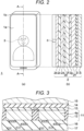
- Figs. 1A and 1B are schematic cross-sectional views of an electronic apparatus 1 according to the first embodiment.
- the electronic apparatus 1 of Fig. 1A is any electronic apparatus 1 having both a display function and an imaging function, such as a smartphone, a mobile phone, a tablet, or a PC.
- the electronic apparatus 1 of Fig. 1A includes a camera module (imaging unit) 3 disposed on the opposite side of a display surface 1a of a display unit 2. As described above, in the electronic apparatus 1 of Fig. 1A , the camera module is provided on the back side of the display surface 1a of the display unit 2. Therefore, the camera module captures an image through the display unit 2 .
- Fig. 2(a) is a schematic external view of the electronic apparatus 1 of Fig. 1A
- Fig. 2(b) is a cross-sectional view taken along line A-A of Fig. 2(a) .
- the display surface 1a extends to the vicinity of the external size of the electronic apparatus 1, and a width of a bezel 1b around the display surface 1a is set to several mm or less.
- a front camera is often mounted on the bezel 1b, but in Fig. 2(a) , as indicated by a broken line, a camera module 3 functioning as the front camera is disposed on a back surface side of a substantially central portion of the display surface 1a.
- the camera module 3 is disposed on the back surface side of the substantially central portion of the display surface 1a, but in the present embodiment, the camera module 3 is only required to be disposed on the back surface side of the display surface 1a, for example, the camera module 3 may be disposed on the back surface side near the peripheral edge portion of the display surface 1a. As described above, the camera module 3 in the present embodiment is disposed at an arbitrary position on the back surface side overlapping with the display surface 1a.
- the display unit 2 is a stacked body obtained by stacking a protective film 2b, a polyimide substrate 2c, a display layer 2d, a barrier layer 2e, a touch sensor layer 2f, an adhesive layer 2g, a circular polarization plate 2h, an optical clear adhesive (OCA) 2i, and a cover glass 2j in this order.
- the display layer 2d may be, for example, an organic light emitting device (OLED) display layer, a liquid crystal display layer, a MicroLED, or a display layer based on other display principles.
- the display layer 2d may include a plurality of layers.
- the display layer 2d may include a color filter layer, a backlight layer, and the like.
- the display unit 2 performs display using light in a visible light wavelength range, but the light displayed in the display unit 2 may include an infrared light component.
- the barrier layer 2e is a layer that prevents oxygen and moisture from entering the display layer 2d.
- a touch sensor is incorporated in the touch sensor layer 2f.
- touch sensors such as a capacitive type and a resistive film type, but any type may be adopted.
- the touch sensor layer 2f and the display layer 2d may be integrated.
- the adhesive layer 2g is provided for bonding the circular polarization plate 2h and the touch sensor layer 2f.
- a material having high visible light transmittance is used for the adhesive layer 2g.
- the circular polarization plate 2h is provided to reduce glare and increase visibility of the display surface 1a even in a bright environment.
- the optical clear adhesive 2i is provided to increase adhesion between the circular polarization plate 2h and the cover glass 2j.
- a material having high visible light transmittance is used as the optical clear adhesive 2i.
- the cover glass 2j is provided to protect the display layer 2d and the like. Note that the layer configuration of the display unit 2 is not necessarily limited to that illustrated in Figs. 1A and 2 .
- the camera module 3 is disposed on the opposite side to the display surface 1a of the display unit 2, that is, on a back side of the display unit 2.
- the camera module 3 includes an imaging unit 4 and an optical system 5.
- the optical system 5 is disposed on a light incident surface side of the imaging unit 4, that is, on a side close to the display unit 2, and condenses the light passing through the display unit 2 on the imaging unit 4.
- the optical system 5 usually includes a plurality of lenses. As described later, there may be a case where a plurality of the camera modules 3 is disposed on the opposite side to the display surface 1a of the display unit 2. In this case, a focal length of the optical system 5 of each of the camera modules 3 may be different from each other such that imaging with a different angle of view such as a wide-angle or a telephoto angle can be performed.
- the imaging unit 4 includes a photoelectric conversion unit 4a.
- the photoelectric conversion unit 4a photoelectrically converts light incident through the display unit 2.
- the photoelectric conversion unit 4a may be a complementary metal oxide semiconductor (CMOS) sensor or a charge coupled device (CCD) sensor.
- CMOS complementary metal oxide semiconductor
- CCD charge coupled device
- the photoelectric conversion unit 4a may be a photodiode or an organic photoelectric conversion film.
- the photoelectric conversion unit 4a includes a photoelectric conversion element such as a CMOS sensor or the like for each pixel.
- the pixels can be arranged in any manner. Specifically, the arrangement form of pixels may be a Bayer arrangement, an interline arrangement, a check pattern arrangement, a stripe arrangement, or other arrangements.
- Fig. 3 is a cross-sectional view illustrating an example of a cross-sectional structure of the imaging unit 4.
- the imaging unit 4 of Fig. 3 includes the photoelectric conversion unit 4a formed in a semiconductor substrate 11, and the photoelectric conversion unit 4a is divided by an element separation layer 12 for each pixel.
- a flattening layer 13 is disposed on the photoelectric conversion unit 4a, and a color filter layer 14 is disposed on the flattening layer 13.
- the color filter layer 14 may include a filter layer of three colors of RGB, or may include a filter layer of cyan, magenta, and yellow which are complementary colors of RGB.
- a filter layer that transmits colors other than visible light such as infrared light may be provided, a filter layer having a multispectral characteristic may be provided, or a filter layer of a decreased color such as white may be provided.
- sensing information such as depth information can be detected.
- An on-chip lens 15 is disposed on the color filter layer 14. The light enters through the on-chip lens 15.
- the side on which the on-chip lens 15 is disposed is referred to as a back surface side of the imaging unit 4.
- a readout circuit 16 is formed on the semiconductor substrate 11, and the periphery of the readout circuit 16 is covered by an interlayer insulation film 17.
- the readout circuit 16 includes a transfer transistor, a reset transistor, an amplification transistor, a selection transistor, and the like. Note that a cross-sectional structure of the imaging unit 4 is not limited to the cross-sectional structure illustrated in Fig. 3 .
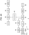
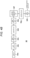
- Fig. 4A is a block diagram illustrating an internal configuration of the electronic apparatus 1 according to the first embodiment.
- the electronic apparatus 1 includes an imaging device 21, an application processor 22, an image signal generation unit 23, an A/D conversion unit 24, a display control unit 25, and the display unit 2.
- the A/D conversion unit 31 converts an analog pixel signal captured by the imaging unit 4 into digital pixel data.
- the signal processing unit 32 includes a clamp unit 32a, a color output unit 32b, a defect correction unit 32c, a linear matrix unit 32d, a gamma correction unit 32e, a luminance/chroma signal generation unit 32f, a noise reduction unit 32g, and an edge emphasis unit 32h.
- the clamp unit 32a performs processing of defining a black level. More specifically, the clamp unit 32a performs processing of subtracting black level data from the digital pixel data.
- the color output unit 32b outputs, for example, pixel data for each color of RGB.
- the defect correction unit 32c performs processing of correcting the imaged data of the specific pixel that cannot be correctly read for some reason in accordance with the imaged data of surrounding pixels.
- the linear matrix unit 32d performs matrix operation on color information for RGB to perform more correct color reproduction.
- the gamma correction unit 32e performs gamma correction so as to enable display excellent in visibility in accordance with a display characteristic of the display unit 2. For example, the gamma correction unit 32e performs conversion from ten bits to eight bits while changing a gradient.
- the luminance/chroma signal generation unit 32f generates a luminance/chroma signal for the display unit 2 to display on the basis of output data of the gamma correction unit 32e.
- the noise reduction unit 32g performs processing of reducing noise included in the luminance/chroma signal.
- the edge emphasis unit 32h performs processing of emphasizing an edge of an object image on the basis of the luminance/chroma signal.
- the noise reduction processing of the noise reduction unit 32g and the edge emphasis processing of the edge emphasis unit 32h may be performed only in a case where a predetermined condition is satisfied.
- the output unit 36 outputs the luminance/chroma signal subjected to the noise reduction processing.
- the imaging control unit 33 sets a frame rate at which the imaging unit 4 performs imaging on the basis of the luminance/chroma signal.
- the exposure adjustment unit 34 adjusts an exposure time according to the frame rate set by the imaging control unit 33.
- the photoelectric conversion unit 4a performs imaging for each pixel according to the exposure time adjusted by the exposure adjustment unit 34.
- the abnormality detection unit 35 detects an abnormality on the display surface of the display unit 2.
- the abnormality includes various deposits on the display surface, scratches on the display surface, deposits and scratches on a protective material such as a film for protecting the display surface, bubbles between the display surface and the protective material, and the like.
- the deposits include stains, hand oil, solidified substances, liquefied substances, and the like.
- the scratches include breaks, cracks, chips, and the like.
- the abnormality detection unit 35 detects a plurality of types of abnormalities.
- the abnormality may be collectively referred to as a foreign substance.
- the abnormality detection unit 35 transmits detected abnormality information to the application processor 22.
- the abnormality information is, for example, information on the type and position of the abnormality.
- the abnormality detection unit 35 transmits captured image data including the abnormality information to the output unit 36.
- the output unit 36 outputs the captured image data together with the abnormality information.
- the output unit 36 may send, to the image signal generation unit 23, the captured image data showing the abnormality.
- the application processor 22 is a semiconductor device separate from the camera module 3, and is mounted on the same substrate as or a different substrate from the camera module 3.
- the application processor 22 includes a central processing unit (CPU) and the like therein, and executes an operating system or programs such as various application software.
- the application processor 22 may have a function of performing image processing of a graphics processing unit (GPU), signal processing of a baseband processor, or the like.
- the application processor 22 executes various processing on the input image data and calculation result as necessary, performs control to display an image on the display unit 2 of the electronic apparatus 1, or transmits the image to an external cloud server via a predetermined network.
- the application processor 22 When receiving the abnormality information sent from the abnormality detection unit 35, the application processor 22 sends the information to the display control unit 25.
- the display control unit 25 highlights a position where the abnormality detected by the abnormality detection unit 35 occurs on the display unit 2. A specific example of highlighting will be described later.
- the image signal generation unit 23 generates an image signal for displaying the image on the display unit 2.
- the A/D conversion unit 24 converts the image signal into digital pixel data.
- the display control unit 25 performs control to display the digital pixel data on the display unit 2. At this time, as described above, the position where the abnormality occurs is highlighted on the basis of the abnormality information detected by the abnormality detection unit 35.
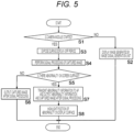
- Fig. 5 is a flowchart illustrating processing operation of the electronic apparatus 1 according to the first embodiment, and illustrates, for example, processing operation of the application processor 22, processing operation of the imaging control unit 33, and processing operation of the display control unit 25. This flowchart is continuously repeated while the electronic apparatus 1 is powered on.
- Step S1 it is determined whether or not a user of the electronic apparatus 1 starts the camera module 3 (Step S2).
- the image generated by the image signal generation unit 23 is displayed on the display unit 2 on the basis of an instruction from the application processor 22 (Step S2).
- Step S3 exposure is performed by the imaging unit 4 during a display-off period of the display unit 2 (Step S3).
- the display on the display unit 2 is updated at a frequency of 30 to 120 frames per second.
- the display is performed while scanning each horizontal line, and there is the display-off period in which the display is not performed between the horizontal lines.
- Step S3 exposure is performed by the imaging unit 4 within these display-off periods.
- the display-off period in Step S3 refers to a period in which the image display, which is displayed on the display unit 2 before the camera module 3 is started, is not performed.
- the signal processing unit 32 performs various signal processing on the captured image obtained by the exposure processing of the imaging unit 4 (Step S4).
- the abnormality detection unit 35 detects whether or not there is an abnormality on the display surface on the basis of the captured image data after the signal processing (Step S5).
- Various methods are conceivable as an abnormality detection method, and specific examples thereof will be described later.
- the captured image data output from the signal processing unit 32 is sent to the output unit 36 (Step S6).
- the abnormality detection unit 35 sends the abnormality information including the position where the abnormality occurs to the application processor 22, and sends the abnormality information and the captured image data to the output unit 36 (Step S7).
- the application processor 22 sends the abnormality information sent from the abnormality detection unit 35 to the display control unit 25.
- the display control unit 25 highlights the position where the abnormality occurs on the display surface (Step S8).
- Figs. 6A, 6B, 6C , and 6D are diagrams illustrating a specific example of highlighting a position where an abnormality 2p occurs.
- Fig. 6A illustrates an example of displaying an annular indicator 2q surrounding the position where the abnormality 2p occurs.
- the indicator 2q of Fig. 6A is desirably displayed in a display color different from the display color of the background image in a noticeable manner. Furthermore, a line width of the indicator 2q may be increased.
- the position where the abnormality 2p occurs is highlighted on the display unit 2. Therefore, it is possible to notify the user in advance that there is a problem in imaging by the imaging unit 4, and to urge the user to remove the abnormality 2p.
- An image quality of the captured image can be improved when the user performs the imaging by the imaging unit 4 after performing a work of eliminating the abnormality 2p, such as wiping the display surface, at the time of highlight of the display unit 2.
- the imaging by the camera module 3 is performed in the display-off period such as between frames or between the horizontal lines, but the light emissions in Figs. 7A to 7C are for detecting the foreign substances and is performed using a part of the display period.
- the electronic apparatus 1 has an internal configuration similar to that in Figs. 4A and 4B , but performs processing operation partially different from that in Fig. 5 .
- Fig. 8 is a flowchart illustrating processing operation of the electronic apparatus 1 according to the second embodiment.
- the processing operation different from that in Fig. 5 will be mainly described.
- the same operation as in Steps S1 and S2 of Fig. 5 is performed (Steps S11 and S12).
- the partial display region 20, which is within the angle-of-view range of the camera module 3, is caused to emit light at a first emission wavelength (Step S13). Since an angle-of-view range varies depending on the focal length of the lens included in the camera module 3, the size of the display region 20 caused to emit the light at the first emission wavelength also needs to be adjusted according to the focal length of the lens. Alternatively, the entire region of the display surface 1a may emit the light at the first emission wavelength.
- Step S13 While the light is emitted in Step S13, the imaging unit 4 performs exposure (Step S14), and the signal processing unit 32 performs various signal processing to generate captured image data (Step S15).
- Steps S13 to S15 is performed in a state in which the display region 20 is caused to emit light at a second emission wavelength as illustrated in Fig. 7B (Steps S16 to S18). Subsequently, the same operation as in Steps S13 to S15 is performed in a state in which the display region 20 is caused to emit light at a third emission wavelength as illustrated in Fig. 7C (Steps S19 to S21).
- the abnormality detection unit 35 detects the presence or absence of the abnormality 2p on the basis of the three pieces of captured image data obtained in Steps S15, S18, and S21 (Steps S22 to S24).
- the imaging unit 4 performs the imaging in a state in which the display region 20, which is at least a part of the display unit 2, is caused to emit light at a plurality of types of emission wavelengths, and the abnormality detection unit 35 detects the abnormality 2p on the basis of a plurality of pieces of the captured image data obtained.
- the type of abnormality 2p only light of a specific emission wavelength is reflected or transmitted. Therefore, by performing the imaging in a state in which the display unit 2 emits light at a plurality of types of emission wavelengths, the presence or absence of the abnormality 2p and the type of abnormality 2p can be easily specified.
- the correction processing for the captured image data is performed.
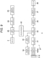
- Fig. 9 is a block diagram illustrating an internal configuration of the electronic apparatus 1 according to the third embodiment.
- the electronic apparatus 1 of Fig. 9 is obtained by adding a correction processing unit 37 to the electronic apparatus 1 of Fig. 4A .
- the correction processing unit 37 corrects the image displayed on the display unit 2 so that the abnormality 2p is not noticeable. More specifically, the correction processing unit 37 performs correction processing on the captured image data output from the signal processing unit 32 on the basis of information regarding the abnormality 2p detected by the abnormality detection unit 35, and outputs the image data after the correction processing.
- the image data output from the correction processing unit 37 is sent to the output unit 36 .
- the correction processing performed by the correction processing unit 37 may include, for example, at least one of edge emphasis processing, distortion correction processing, and scratch correction processing.
- the abnormality detection unit 35 in the electronic apparatus 1 according to the third embodiment may cause the display surface 1a to emit light at a plurality of emission wavelengths to detect the abnormality 2p of the display surface 1a as in the second embodiment.
- the abnormality detection unit 35 according to the present embodiment can detect the type of abnormality 2p , and an absorption characteristic and a scattering characteristic for a specific emission wavelength change in accordance with the type of abnormality 2p .
- the abnormality detection unit 35 can relatively accurately estimate the type of abnormality 2p from a correspondence relationship between the emission wavelength and the absorption characteristic or scattering characteristic.
- the correction processing unit 37 can perform appropriate correction processing according to the type of abnormality 2p.
- Fig. 10 is a flowchart illustrating a processing procedure of the correction processing performed by the correction processing unit 37.
- the correction processing of Fig. 10 is performed instead of Steps S7 and S8 of Fig. 5 or Steps S24 and S25 of Fig. 8 in a case where it is determined that there is an abnormality on the display surface 1a in Step S5 of Fig. 5 or Step S22 of Fig. 8 .
- the type of abnormality 2p is determined on the basis of the information regarding the abnormality 2p detected by the abnormality detection unit 35 (Step S31).
- Step S32 it is determined whether or not the correction processing unit 37 of the electronic apparatus 1 can perform effective correction processing.
- the electronic apparatus 1 is a portable apparatus such as a smartphone
- hardware performance is inferior to that of a PC, a server, or the like, and it is difficult to perform advanced correction processing. Therefore, in a case where the correction processing satisfying the user cannot be performed within several seconds, it is determined that the effective correction processing cannot be performed.
- the determination processing in Step S32 is performed by the correction processing unit 37, for example.
- the correction processing unit 37 performs the correction processing according to the type of abnormality 2p (Step S33). For example, when the abnormality detection unit 35 detects that the abnormality 2p is hand oil adhering on the display surface 1a, the edge of the captured image captured via the hand oil tends to be blurred. Therefore, the edge emphasis processing is performed. In this case, the edge emphasis processing may be performed inside the correction processing unit 37, or the correction processing unit 37 may instruct the edge emphasis unit 32h of the signal processing unit 32 to enhance the edge emphasis processing.
- the correction processing unit 37 may perform distortion correction processing, and when the abnormality detection unit 35 detects that the abnormality 2p is a scratch on the display surface 1a, the correction processing unit 37 may perform correction processing of removing the scratch.
- the image data after the correction processing is sent to the output unit 36 (Step S34).
- Step S32 when it is determined that the effective correction processing cannot be performed in Step S32, the captured image data output from the signal processing unit 32 and the information regarding the abnormality 2p detected by the abnormality detection unit 35 are transmitted to a specific information processing apparatus that performs advanced correction processing (Step S35).
- the information processing apparatus may be, for example, a server apparatus connected to a network or a high-performance PC. Thereafter, in the information processing apparatus, the correction processing is performed on the captured image data and the correction processing unit 37 receives the image data after the correction processing (Step S36). The received image data after the correction processing is sent to the output unit 36.
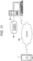
- Fig. 11 is a block diagram illustrating an example of a connection form between the electronic apparatus 1 and an information processing apparatus 41.
- the electronic apparatus 1 and the information processing apparatus 41 transmit and receive information via a network 42.
- the information processing apparatus 41 may be provided in an unspecified place separated from the electronic apparatus 1, that is, in a cloud environment, or may be provided in a place (for example, a base station or the like) relatively close to the electronic apparatus 1 in a similar manner to a mobile edge computing (MEC).
- MEC mobile edge computing
- a database apparatus 43 is connected to the information processing apparatus 41, and the database apparatus 43 stores information regarding a correspondence relationship between the type of abnormality 2p and the correction processing and information regarding a model that performs the correction processing according to the type of abnormality 2p.
- the information processing apparatus 41 learns a model by using the type of abnormality 2p and the captured image data as input data for the model such that the captured image data subjected to appropriate correction processing is output. In the process of learning, weight information of a neural network is variously changed to update the model.
- the information processing apparatus 41 accumulates various types of abnormality 2p and a result of the correction processing in the database apparatus 43, repeats learning of the model, and thus a highly reliable model can be generated. By learning such a model in advance, it is possible to perform highly reliable correction processing in a short time on the type of abnormality 2p and the captured image data, which are sent from the electronic apparatus 1 and return the image data after the correction processing to the electronic apparatus 1.
- the correction processing for the captured image data is performed such that the abnormality 2p is not noticeable. Therefore, high-quality captured image data can be obtained without the user performing the work of removing the abnormality 2p on the display surface 1a.
- a plurality of the camera modules 3 is disposed on the opposite side to the display surface 1a of the display unit 2.
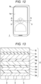
- Fig. 12 is a plan view of the electronic apparatus 1 according to the fourth embodiment.
- three camera modules 3 are disposed on the opposite side to the display surface 1a of the display unit 2. Note that the number of camera modules 3 is not limited to three. A focal length of each camera module 3 may be the same or different.
- Fig. 13 is a cross-sectional view taken along line A-A of Fig. 12 .
- the imaging range of each camera module 3 is indicated by a broken line.
- at least two camera modules 3 can image an arbitrary place on the display surface 1a of the display unit 2. Therefore, the abnormality 2p occurring at an arbitrary place on the display surface 1a can be imaged by a plurality of the camera modules 3.
- the type of abnormality 2p can be easily specified by imaging an abnormal place on the display surface 1a in different directions.
- the abnormality detection unit 35 detects the type of abnormality 2p with reference to a plurality of pieces of captured image data captured by a plurality of the camera modules 3.
- the imaging may be performed in a state in which the display surface 1a is caused to emit light at a plurality of different emission wavelengths.
- the correction processing unit 37 performs correction processing for removing the abnormality 2p on the basis of a plurality of pieces of captured image data captured by a plurality of the camera modules 3. It is possible to perform effective correction processing when performing the correction processing on the basis of a plurality of captured image data captured in a plurality of directions as compared with when performing the correction processing on the basis of captured image data captured in one direction. Note that, in a case where the correction processing unit 37 determines that the effective correction processing cannot be performed, a plurality of pieces of the captured image data captured by a plurality of the camera modules 3 may be transmitted to the external information processing apparatus 41, and the information processing apparatus 41 may perform the correction processing.
- the abnormality 2p in an arbitrary place on the display surface 1a can be imaged by at least two camera modules 3. Therefore, it is possible to more accurately detect the presence or absence of the abnormality 2p and the type of the abnormality 2p, and perform the correction processing for removing the abnormality 2p.
- the fifth embodiment relates to a specific detection method of the abnormality 2p, and can be applied to the abnormality detection unit 35 according to the first to fourth embodiments.
- Fig. 14 is a plan view illustrating an example of a pixel arrangement of the imaging unit 4 according to the fifth embodiment.
- pixels for three colors of RGB are disposed in a two-dimensional direction.
- Each of the pixels includes a photoelectric conversion unit 4a, and converts incident light into an electric signal corresponding to a light amount.
- Some of a plurality of the pixels are pixels for phase difference detection, and a pixel region is divided into two.
- Each of the divided pixels 10a and 10b in the pixel for the phase difference detection individually performs photoelectric conversion.
- a difference between the electrical signals photoelectrically converted by two divided pixels 10a and 10b is phase difference information, and a defocus amount can be detected on the basis of the phase difference information.
- the defocus amount can be used to adjust focus.
- the example is described in which the pixels for phase difference detection are disposed at four corners, but where and how many the pixels for phase difference detection are disposed are arbitrary.
- the presence or absence of the abnormality 2p can be detected by using the defocus amount obtained by the two divided pixels 10a and 10b constituting the pixel for the phase difference detection. That is, in a case where there is a foreign substance on the display surface 1a, the pixel for the phase difference detection recognizes the foreign substance as a part of the object and detects the defocus amount.
- the foreign substance can be detected by using the detected defocus amount.
- at least two camera modules 3 detect the defocus amount caused by the foreign substance, and thus it is possible to specify that the detected defocus amount is not caused by an originally intended object but caused by the foreign substance on the display surface 1a.
- the fifth embodiment by providing the pixels for phase difference detection in a part of the pixel arrangement for imaging, it is possible to accurately detect the abnormality 2p on the display surface 1a.
- the sixth embodiment detects the abnormality 2p on the display surface 1a by a method different from that of the fifth embodiment. Processing of detecting the abnormality 2p according to the sixth embodiment can be applied to the abnormality detection unit 35 according to the first to fourth embodiments.
- Fig. 15 is a plan view illustrating an example of a pixel arrangement of the imaging unit 4 according to the sixth embodiment.
- pixels for three colors of RGB are disposed in a two-dimensional direction.
- Each of the pixels includes a photoelectric conversion unit 4a.
- a polarization element 8b is disposed on a light incident surface side of the photoelectric conversion unit 4a.
- the pixel in which the polarization element 8b is disposed is referred to as a polarization pixel 10c
- the pixel in which the polarization element 8b is disposed is referred to as a non-polarization pixel 10d.
- the polarization element 8b polarizes light that is incident through the display unit 2.
- the light polarized by the polarization element 8b is incident on the corresponding photoelectric conversion unit 4a and is photoelectrically converted.
- Fig. 16 is a cross-sectional view of the imaging unit 4 according to the sixth embodiment.
- the same components as those in Fig. 3 are denoted by the same reference numerals, and differences will be mainly described below.
- a light shielding layer 18 and an underlying insulation layer 19 are disposed on the flattening layer 13, and a plurality of the polarization elements 8b is disposed on the underlying insulation layer 19 in a state of being separated from each other.
- the polarization element 8b is, for example, a wire grid polarization element 8b having a line-and-space structure disposed on a part of the underlying insulation layer 19.
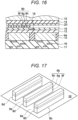
- Fig. 17 is a perspective view illustrating an example of a detailed structure of each polarization element 8b.
- each of a plurality of the polarization elements 8b includes a plurality of line portions 8d having a protruding shape extending in one direction and a space portion 8e between the line portions 8d.
- the angle between the arrangement direction of the photoelectric conversion unit 4a and the extending direction of the line portion 8d may be four types of angles of zero degrees, 45 degrees, 90 degrees, and 135 degrees, or may be other angles.
- a plurality of the polarization elements 8b may polarize light only in a single direction.
- a material of a plurality of the polarization elements 8b may be a metal material such as aluminum or tungsten, or an organic photoelectric conversion film.
- each of the polarization elements 8b passes light each having a different polarization state, and the corresponding photoelectric conversion unit 4a performs the photoelectric conversion.
- the types of light passing through four types of polarization elements 8b change in accordance with the type of abnormality 2p. Therefore, the type of abnormality 2p can be specified by analyzing electric signals photoelectrically converted by four types of polarization pixels 10c.
- the polarization pixel 10c can also be used for extracting and removing components of flare and diffraction light which are incident on the display surface 1a.
- the polarization output unit 32j outputs polarization information data.
- the flare extraction unit 32k extracts at least one of the flare component or the diffraction light component from the polarization information data. At least one of the flare component and the diffraction light component extracted by the flare extraction unit 32k is a correction amount.
- the flare correction signal generation unit 32m corrects digital pixel data by subtracting the correction amount extracted by the flare extraction unit 32k from the digital pixel data output from the color output unit 32b.
- the output data of the flare correction signal generation unit 32m is digital pixel data from which at least one of the flare component or the diffraction light component is removed.
- the flare correction signal generation unit 32m functions as a correction unit that corrects the captured image photoelectrically converted by a plurality of the non-polarization pixels 10d on the basis of the polarization information.
- a signal level of the digital pixel data at the pixel position of the polarization pixel 10c is lower by an amount of light passing through the polarization element 8b. Therefore, the defect correction unit 32c regards the polarization pixel 10c as a defect and performs predetermined defect correction processing.
- the polarization pixel 10c using the polarization element 8b is provided in a part of the pixel arrangement for imaging, the abnormality 2p on the display surface 1a can be detected using the polarization pixel 10c. Furthermore, in the polarization pixel 10c, the flare and diffraction light incident on the display surface 1a can be extracted and removed.
- the abnormality 2p on the display surface 1a is detected using a sensor that optically detects a distance to the object.
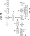
- Fig. 19 is a block diagram illustrating a schematic configuration of the electronic apparatus 1 according to the seventh embodiment.
- the electronic apparatus 1 of Fig. 19 includes a distance measurement unit 27 in addition to the block configuration of the electronic apparatus 1 of Fig. 4A .
- the distance measurement unit 27 includes a light projection unit 27a and a light reception unit 27b.
- the light projection unit 27a intermittently emits pulsed light having a predetermined wavelength, and the light reception unit 27b receives the light emitted by the light projection unit 27a and reflected by the object.
- the distance measurement unit 27 measures a distance to the object on the basis of a difference between a time when light is emitted by the light projection unit 27a and a time when the light is received by the light reception unit 27b.
- the light projection unit 27a may perform scanning in the light projecting direction within a predetermined angle range. Therefore, the light from the light projection unit 27a can be emitted to the entire region of the display surface 1a.
- the abnormality detection unit 35 can accurately detect whether or not the object is a foreign substance on the display surface 1a by using the distance measured by the distance measurement unit 27.
- the distance measurement unit 27 that optically detects the distance to the object since the distance measurement unit 27 that optically detects the distance to the object is provided, it is possible to simply and accurately detect whether or not there is the abnormality 2p on the display surface 1a.
- a plurality of cameras that captures images at different angles of view may be provided, and the distance to the object may be measured on the basis of the captured images captured by a plurality of the cameras.
- the imaging unit 4 of the electronic apparatus 1 is used to image the object, but the imaging unit 4 can be used for biometric authentication applications such as fingerprint detection, iris detection, retina detection, vein detection, and biometric detection. Since an appropriate focal length varies depending on the detection target of the living body, the electronic apparatus 1 of the first to seventh embodiments can be applied to detection of various pieces of biological information by providing a lens having a focal length matching the detection target and optimizing a prism, a light source, and the like.
- the optical system 5 of the camera module 3 is different from that of the first to eighth embodiments.
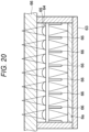
- Fig. 20 is a diagram illustrating a cross-sectional structure of the imaging unit 4 of the camera module 3 mounted on an electronic apparatus 1 according to the ninth embodiment.
- the imaging unit 4 of Fig. 20 includes a microlens array 64 instead of a single lens or a lens group in which single lenses are arranged in an optical axis direction.
- the imaging unit 4 of Fig. 20 includes a photoelectric conversion unit 4a disposed along a bottom surface of a housing 63, the microlens array 64 disposed above the photoelectric conversion unit 4a, a plurality of light shielding bodies 66 disposed between adjacent microlenses 65, and a light guide plate 67 disposed above the microlens array 64.
- the imaging unit 4 of Fig. 20 is applicable to any of the first to eighth embodiments described above.
- Fig. 21 is a plan view in a case where the electronic apparatus 1 according to the first to ninth embodiments is applied to a capsule endoscope 50.
- the capsule endoscope 50 of Fig. 21 includes, for example, a camera (ultra-small camera) 52 for capturing an image in a body cavity, a memory 53 for recording image data captured by the camera 52, and a wireless transmitter 55 for transmitting the recorded image data to the outside via an antenna 54 after the capsule endoscope 50 is discharged to the outside of a subject, in a housing 51 having both end surfaces hemispherical and a cylindrical central portion.
- a camera ultra-small camera
- a central processing unit (CPU) 56 and a coil (magnetic force/current conversion coil) 57 are provided.
- the CPU 56 controls imaging by the camera 52 and data accumulation operation in the memory 53, and controls data transmission of the wireless transmitter 55 from the memory 53 to a data reception device (not illustrated) outside the housing 51.
- the coil 57 supplies power to the camera 52, the memory 53, the wireless transmitter 55, the antenna 54, and a light source 52b to be described later.
- the housing 51 is provided with a magnetic (reed) switch 58 for detecting a state in which the capsule endoscope 50 is set in the data reception device.
- the CPU 56 supplies power from the coil 57 to the wireless transmitter 55 when the reed switch 58 detects the state of being set to the data reception device and data transmission becomes possible.
- the camera 52 includes, for example, an image sensor 52a including an objective optical system for capturing an image in the body cavity, and a plurality of the light sources 52b for illuminating the body cavity.
- the camera 52 includes, as the light source 52b, for example, a complementary metal oxide semiconductor (CMOS) sensor or a charge coupled device (CCD), which includes a light emitting diode (LED).
- CMOS complementary metal oxide semiconductor
- CCD charge coupled device
- the display unit 2 of the electronic apparatus 1 is a display unit including a light emitting body such as the light source 52b of Fig. 21 .
- the capsule endoscope 50 of Fig. 21 includes, for example, two light sources 52b, but these light sources 52b can be configured by a display panel having a plurality of light source units or an LED module having a plurality of LEDs. In this case, by disposing the imaging unit 4 of the camera 52 below the display panel or the LED module, restrictions on the layout arrangement of the camera 52 are reduced, and the capsule endoscope 50 having a smaller size can be realized.
- Fig. 22 is a rear view in a case where the electronic apparatus 1 according to the first to ninth embodiments is applied to a digital single-lens reflex camera 60.
- the digital single-lens reflex camera 60 and a compact camera include the display unit 2 that displays a preview screen on a back surface on an opposite side to the lens.
- the camera module 3 may be disposed on the opposite side to the display surface of the display unit 2 such that a face image of a photographer can be displayed on the display surface 1a of the display unit 2.
- the camera module 3 can be disposed in a region overlapping the display unit 2, it is not necessary to provide the camera module 3 in a frame portion of the display unit 2, and the size of the display unit 2 can be increased as much as possible.
- Fig. 23A is a plan view illustrating an example in which the electronic apparatus 1 according to the first to ninth embodiments is applied to a head mounted display (HMD) 61.
- the HMD 61 of Fig. 23A is used for virtual reality (VR), augmented reality (AR), mixed reality (MR), substituional reality (SR), and the like.
- a camera 62 is mounted on the outer surface, and the wearer of the HMD can visually recognize the surrounding image, but there is a problem that the surrounding people cannot recognize the expression of eyes or a face of the wearer of the HMD.
- the display surface of the display unit 2 is provided on the outer surface of the HMD 61, and the camera module 3 is provided on the opposite side to the display surface of the display unit 2. Therefore, the expression of the face of the wearer, which is imaged by the camera module 3, can be displayed on the display surface of the display unit 2, and the people around the wearer can grasp the expression of the face of the wearer and the movement of the eyes of the wearer in real time.
- Fig. 23A since the camera module 3 is provided on the back surface side of the display unit 2, there is no restriction on the installation location of the camera module 3, and the degree of freedom in design of the HMD 61 can be increased. Furthermore, since the camera can be disposed at an optimum position, it is possible to prevent problems such as misalignment of the eyes of the wearer displayed on the display surface.
- the electronic apparatus 1 according to the first to ninth embodiments can be used for various applications, and a utility value can be increased.
Landscapes
- Engineering & Computer Science (AREA)
- Signal Processing (AREA)
- Multimedia (AREA)
- Physics & Mathematics (AREA)
- General Physics & Mathematics (AREA)
- Theoretical Computer Science (AREA)
- Computer Vision & Pattern Recognition (AREA)
- Quality & Reliability (AREA)
- Computer Hardware Design (AREA)
- Studio Devices (AREA)
- Geometry (AREA)
- Mechanical Treatment Of Semiconductor (AREA)
Applications Claiming Priority (2)
| Application Number | Priority Date | Filing Date | Title |
|---|---|---|---|
| JP2020008524 | 2020-01-22 | ||
| PCT/JP2021/000399 WO2021149503A1 (ja) | 2020-01-22 | 2021-01-07 | 電子機器 |
Publications (3)
| Publication Number | Publication Date |
|---|---|
| EP4096212A1 EP4096212A1 (en) | 2022-11-30 |
| EP4096212A4 EP4096212A4 (en) | 2023-06-21 |
| EP4096212B1 true EP4096212B1 (en) | 2025-04-16 |
Family
ID=76878482
Family Applications (1)
| Application Number | Title | Priority Date | Filing Date |
|---|---|---|---|
| EP21743939.7A Active EP4096212B1 (en) | 2020-01-22 | 2021-01-07 | Electronic device |
Country Status (8)
| Country | Link |
|---|---|
| US (1) | US12165552B2 (cg-RX-API-DMAC7.html) |
| EP (1) | EP4096212B1 (cg-RX-API-DMAC7.html) |
| JP (1) | JP7646573B2 (cg-RX-API-DMAC7.html) |
| KR (1) | KR20220131236A (cg-RX-API-DMAC7.html) |
| CN (1) | CN113163106B (cg-RX-API-DMAC7.html) |
| DE (1) | DE112021000671T5 (cg-RX-API-DMAC7.html) |
| TW (1) | TW202147822A (cg-RX-API-DMAC7.html) |
| WO (1) | WO2021149503A1 (cg-RX-API-DMAC7.html) |
Families Citing this family (4)
| Publication number | Priority date | Publication date | Assignee | Title |
|---|---|---|---|---|
| JP7764464B2 (ja) * | 2021-03-19 | 2025-11-05 | 富士フイルム株式会社 | 画像データ処理装置、画像データ処理方法、画像データ処理プログラム及び撮像システム |
| JP2023045100A (ja) * | 2021-09-21 | 2023-04-03 | ソニーセミコンダクタソリューションズ株式会社 | 電子機器 |
| JP2023170242A (ja) * | 2022-05-18 | 2023-12-01 | キヤノンメディカルシステムズ株式会社 | 医用画像診断装置 |
| GB2636789A (en) * | 2023-12-21 | 2025-07-02 | Nokia Technologies Oy | An apparatus |
Family Cites Families (20)
| Publication number | Priority date | Publication date | Assignee | Title |
|---|---|---|---|---|
| JP2004153422A (ja) * | 2002-10-29 | 2004-05-27 | Toshiba Corp | 撮影装置、顔照合装置、撮影装置の汚れ検知方法、及び顔照合方法 |
| JP4333199B2 (ja) * | 2003-04-17 | 2009-09-16 | 株式会社ニコン | レンズ交換式デジタルカメラの異物検出治具、カメラ本体および異物検出システム |
| JP2006338122A (ja) * | 2005-05-31 | 2006-12-14 | Olympus Imaging Corp | 携帯端末装置 |
| JP4678860B2 (ja) * | 2006-01-24 | 2011-04-27 | キヤノン株式会社 | 撮像装置及びその制御方法とプログラム |
| JP4757085B2 (ja) * | 2006-04-14 | 2011-08-24 | キヤノン株式会社 | 撮像装置及びその制御方法、画像処理装置、画像処理方法、及びプログラム |
| JP5207057B2 (ja) * | 2008-11-28 | 2013-06-12 | サクサ株式会社 | 撮影装置の汚れを検知する汚れ検知装置及び同検知方法 |
| JP2011044094A (ja) * | 2009-08-24 | 2011-03-03 | Sharp Corp | 表示装置 |
| CN102648405B (zh) | 2009-11-20 | 2015-04-15 | 独立行政法人产业技术综合研究所 | 检查缺陷方法和装置、晶圆、半导体元件 |
| JP2011114542A (ja) * | 2009-11-26 | 2011-06-09 | Nikon Corp | デジタルカメラ |
| JP2013057570A (ja) | 2011-09-07 | 2013-03-28 | Jfe Steel Corp | 表面欠陥検出装置 |
| US8947627B2 (en) | 2011-10-14 | 2015-02-03 | Apple Inc. | Electronic devices having displays with openings |
| JP6156820B2 (ja) * | 2013-08-22 | 2017-07-05 | 住友化学株式会社 | 欠陥検査装置、光学部材の製造システム及び光学表示デバイスの生産システム |
| JP6276092B2 (ja) * | 2014-03-31 | 2018-02-07 | 国立大学法人 東京大学 | 検査システムおよび検査方法 |
| JP6506506B2 (ja) | 2014-04-02 | 2019-04-24 | キヤノン株式会社 | 画像処理装置、撮像装置、制御方法およびプログラム |
| JP6693712B2 (ja) | 2015-07-01 | 2020-05-13 | 株式会社ソニー・インタラクティブエンタテインメント | 撮像装置および情報処理装置 |
| US10897148B2 (en) | 2016-09-23 | 2021-01-19 | Apple Inc. | Wireless charging mats with multi-layer transmitter coil arrangements |
| CN110044931B (zh) | 2019-04-23 | 2021-03-26 | 华中科技大学 | 一种曲面玻璃表面和内部缺陷的检测装置 |
| US11076071B2 (en) * | 2019-05-08 | 2021-07-27 | Lenovo (Singapore) Pte. Ltd. | Device having a camera overlaid by display and method for implementing same |
| US10812699B1 (en) * | 2019-05-08 | 2020-10-20 | Lenovo (Singapore) Pte. Ltd. | Device having a camera overlaid by display and method for implementing the same |
| CN110286130B (zh) * | 2019-07-26 | 2020-05-15 | 上海御微半导体技术有限公司 | 一种缺陷检测装置及其方法 |
-
2021
- 2021-01-07 EP EP21743939.7A patent/EP4096212B1/en active Active
- 2021-01-07 WO PCT/JP2021/000399 patent/WO2021149503A1/ja not_active Ceased
- 2021-01-07 US US17/790,785 patent/US12165552B2/en active Active
- 2021-01-07 JP JP2021573060A patent/JP7646573B2/ja active Active
- 2021-01-07 KR KR1020227024526A patent/KR20220131236A/ko active Pending
- 2021-01-07 DE DE112021000671.1T patent/DE112021000671T5/de active Pending
- 2021-01-14 CN CN202110050279.4A patent/CN113163106B/zh active Active
- 2021-01-15 TW TW110101557A patent/TW202147822A/zh unknown
Also Published As
| Publication number | Publication date |
|---|---|
| CN113163106A (zh) | 2021-07-23 |
| JP7646573B2 (ja) | 2025-03-17 |
| US12165552B2 (en) | 2024-12-10 |
| JPWO2021149503A1 (cg-RX-API-DMAC7.html) | 2021-07-29 |
| EP4096212A1 (en) | 2022-11-30 |
| DE112021000671T5 (de) | 2022-11-10 |
| CN113163106B (zh) | 2026-01-30 |
| EP4096212A4 (en) | 2023-06-21 |
| WO2021149503A1 (ja) | 2021-07-29 |
| KR20220131236A (ko) | 2022-09-27 |
| US20230042435A1 (en) | 2023-02-09 |
| TW202147822A (zh) | 2021-12-16 |
Similar Documents
| Publication | Publication Date | Title |
|---|---|---|
| US12165552B2 (en) | Electronic apparatus | |
| CN112887625B (zh) | 电子设备 | |
| US8497897B2 (en) | Image capture using luminance and chrominance sensors | |
| CN112637387B (zh) | 电子设备 | |
| CN115486056B (zh) | 电子设备和成像装置 | |
| CN214381044U (zh) | 电子设备 | |
| EP4060405B1 (en) | Electronic device | |
| CN115023938B (zh) | 电子装置 | |
| CN113468942B (zh) | 电子设备 | |
| WO2023106010A1 (ja) | 電子機器 |
Legal Events
| Date | Code | Title | Description |
|---|---|---|---|
| STAA | Information on the status of an ep patent application or granted ep patent |
Free format text: STATUS: THE INTERNATIONAL PUBLICATION HAS BEEN MADE |
|
| PUAI | Public reference made under article 153(3) epc to a published international application that has entered the european phase |
Free format text: ORIGINAL CODE: 0009012 |
|
| STAA | Information on the status of an ep patent application or granted ep patent |
Free format text: STATUS: REQUEST FOR EXAMINATION WAS MADE |
|
| 17P | Request for examination filed |
Effective date: 20220713 |
|
| AK | Designated contracting states |
Kind code of ref document: A1 Designated state(s): AL AT BE BG CH CY CZ DE DK EE ES FI FR GB GR HR HU IE IS IT LI LT LU LV MC MK MT NL NO PL PT RO RS SE SI SK SM TR |
|
| DAV | Request for validation of the european patent (deleted) | ||
| DAX | Request for extension of the european patent (deleted) | ||
| REG | Reference to a national code |
Ref country code: DE Ref legal event code: R079 Ipc: H04N0023810000 Ref country code: DE Ref legal event code: R079 Ref document number: 602021029256 Country of ref document: DE Free format text: PREVIOUS MAIN CLASS: H04N0005232000 Ipc: H04N0023810000 |
|
| A4 | Supplementary search report drawn up and despatched |
Effective date: 20230524 |
|
| RIC1 | Information provided on ipc code assigned before grant |
Ipc: G06T 7/00 20170101ALI20230517BHEP Ipc: G06T 5/00 20060101ALI20230517BHEP Ipc: H04M 1/02 20060101ALI20230517BHEP Ipc: H04N 23/73 20230101ALI20230517BHEP Ipc: H04N 23/57 20230101ALI20230517BHEP Ipc: H04N 23/81 20230101AFI20230517BHEP |
|
| REG | Reference to a national code |
Ref country code: DE Ref legal event code: R079 Free format text: PREVIOUS MAIN CLASS: H04N0023810000 Ipc: H04N0023670000 Ref country code: DE Ref legal event code: R079 Ref document number: 602021029256 Country of ref document: DE Free format text: PREVIOUS MAIN CLASS: H04N0023810000 Ipc: H04N0023670000 |
|
| GRAP | Despatch of communication of intention to grant a patent |
Free format text: ORIGINAL CODE: EPIDOSNIGR1 |
|
| STAA | Information on the status of an ep patent application or granted ep patent |
Free format text: STATUS: GRANT OF PATENT IS INTENDED |
|
| RIC1 | Information provided on ipc code assigned before grant |
Ipc: H04N 25/671 20230101ALI20241113BHEP Ipc: H04M 1/02 20060101ALI20241113BHEP Ipc: G06T 5/80 20240101ALI20241113BHEP Ipc: G06T 5/77 20240101ALI20241113BHEP Ipc: G06T 5/73 20240101ALI20241113BHEP Ipc: H01L 27/146 20060101ALI20241113BHEP Ipc: H04N 23/73 20230101ALI20241113BHEP Ipc: H04N 23/57 20230101ALI20241113BHEP Ipc: H04N 23/81 20230101ALI20241113BHEP Ipc: H04N 23/67 20230101AFI20241113BHEP |
|
| INTG | Intention to grant announced |
Effective date: 20241125 |
|
| GRAS | Grant fee paid |
Free format text: ORIGINAL CODE: EPIDOSNIGR3 |
|
| GRAA | (expected) grant |
Free format text: ORIGINAL CODE: 0009210 |
|
| STAA | Information on the status of an ep patent application or granted ep patent |
Free format text: STATUS: THE PATENT HAS BEEN GRANTED |
|
| P01 | Opt-out of the competence of the unified patent court (upc) registered |
Free format text: CASE NUMBER: APP_8100/2025 Effective date: 20250218 |
|
| AK | Designated contracting states |
Kind code of ref document: B1 Designated state(s): AL AT BE BG CH CY CZ DE DK EE ES FI FR GB GR HR HU IE IS IT LI LT LU LV MC MK MT NL NO PL PT RO RS SE SI SK SM TR |
|
| REG | Reference to a national code |
Ref country code: GB Ref legal event code: FG4D |
|
| REG | Reference to a national code |
Ref country code: CH Ref legal event code: EP |
|
| REG | Reference to a national code |
Ref country code: IE Ref legal event code: FG4D |
|
| REG | Reference to a national code |
Ref country code: DE Ref legal event code: R096 Ref document number: 602021029256 Country of ref document: DE |
|
| REG | Reference to a national code |
Ref country code: NL Ref legal event code: MP Effective date: 20250416 |
|
| PG25 | Lapsed in a contracting state [announced via postgrant information from national office to epo] |
Ref country code: NL Free format text: LAPSE BECAUSE OF FAILURE TO SUBMIT A TRANSLATION OF THE DESCRIPTION OR TO PAY THE FEE WITHIN THE PRESCRIBED TIME-LIMIT Effective date: 20250416 |
|
| REG | Reference to a national code |
Ref country code: AT Ref legal event code: MK05 Ref document number: 1786662 Country of ref document: AT Kind code of ref document: T Effective date: 20250416 |
|
| PG25 | Lapsed in a contracting state [announced via postgrant information from national office to epo] |
Ref country code: FI Free format text: LAPSE BECAUSE OF FAILURE TO SUBMIT A TRANSLATION OF THE DESCRIPTION OR TO PAY THE FEE WITHIN THE PRESCRIBED TIME-LIMIT Effective date: 20250416 Ref country code: PT Free format text: LAPSE BECAUSE OF FAILURE TO SUBMIT A TRANSLATION OF THE DESCRIPTION OR TO PAY THE FEE WITHIN THE PRESCRIBED TIME-LIMIT Effective date: 20250818 Ref country code: ES Free format text: LAPSE BECAUSE OF FAILURE TO SUBMIT A TRANSLATION OF THE DESCRIPTION OR TO PAY THE FEE WITHIN THE PRESCRIBED TIME-LIMIT Effective date: 20250416 |
|
| REG | Reference to a national code |
Ref country code: LT Ref legal event code: MG9D |
|
| PG25 | Lapsed in a contracting state [announced via postgrant information from national office to epo] |
Ref country code: NO Free format text: LAPSE BECAUSE OF FAILURE TO SUBMIT A TRANSLATION OF THE DESCRIPTION OR TO PAY THE FEE WITHIN THE PRESCRIBED TIME-LIMIT Effective date: 20250716 Ref country code: GR Free format text: LAPSE BECAUSE OF FAILURE TO SUBMIT A TRANSLATION OF THE DESCRIPTION OR TO PAY THE FEE WITHIN THE PRESCRIBED TIME-LIMIT Effective date: 20250717 |
|
| PG25 | Lapsed in a contracting state [announced via postgrant information from national office to epo] |
Ref country code: PL Free format text: LAPSE BECAUSE OF FAILURE TO SUBMIT A TRANSLATION OF THE DESCRIPTION OR TO PAY THE FEE WITHIN THE PRESCRIBED TIME-LIMIT Effective date: 20250416 |
|
| PG25 | Lapsed in a contracting state [announced via postgrant information from national office to epo] |
Ref country code: BG Free format text: LAPSE BECAUSE OF FAILURE TO SUBMIT A TRANSLATION OF THE DESCRIPTION OR TO PAY THE FEE WITHIN THE PRESCRIBED TIME-LIMIT Effective date: 20250416 |
|
| PG25 | Lapsed in a contracting state [announced via postgrant information from national office to epo] |
Ref country code: HR Free format text: LAPSE BECAUSE OF FAILURE TO SUBMIT A TRANSLATION OF THE DESCRIPTION OR TO PAY THE FEE WITHIN THE PRESCRIBED TIME-LIMIT Effective date: 20250416 |
|
| PG25 | Lapsed in a contracting state [announced via postgrant information from national office to epo] |
Ref country code: AT Free format text: LAPSE BECAUSE OF FAILURE TO SUBMIT A TRANSLATION OF THE DESCRIPTION OR TO PAY THE FEE WITHIN THE PRESCRIBED TIME-LIMIT Effective date: 20250416 |
|
| PG25 | Lapsed in a contracting state [announced via postgrant information from national office to epo] |
Ref country code: RS Free format text: LAPSE BECAUSE OF FAILURE TO SUBMIT A TRANSLATION OF THE DESCRIPTION OR TO PAY THE FEE WITHIN THE PRESCRIBED TIME-LIMIT Effective date: 20250716 |
|
| PG25 | Lapsed in a contracting state [announced via postgrant information from national office to epo] |
Ref country code: IS Free format text: LAPSE BECAUSE OF FAILURE TO SUBMIT A TRANSLATION OF THE DESCRIPTION OR TO PAY THE FEE WITHIN THE PRESCRIBED TIME-LIMIT Effective date: 20250816 |
|
| PG25 | Lapsed in a contracting state [announced via postgrant information from national office to epo] |
Ref country code: LV Free format text: LAPSE BECAUSE OF FAILURE TO SUBMIT A TRANSLATION OF THE DESCRIPTION OR TO PAY THE FEE WITHIN THE PRESCRIBED TIME-LIMIT Effective date: 20250416 |
|
| PG25 | Lapsed in a contracting state [announced via postgrant information from national office to epo] |
Ref country code: DK Free format text: LAPSE BECAUSE OF FAILURE TO SUBMIT A TRANSLATION OF THE DESCRIPTION OR TO PAY THE FEE WITHIN THE PRESCRIBED TIME-LIMIT Effective date: 20250416 Ref country code: SM Free format text: LAPSE BECAUSE OF FAILURE TO SUBMIT A TRANSLATION OF THE DESCRIPTION OR TO PAY THE FEE WITHIN THE PRESCRIBED TIME-LIMIT Effective date: 20250416 |
|
| REG | Reference to a national code |
Ref country code: DE Ref legal event code: R097 Ref document number: 602021029256 Country of ref document: DE |
|
| PG25 | Lapsed in a contracting state [announced via postgrant information from national office to epo] |
Ref country code: CZ Free format text: LAPSE BECAUSE OF FAILURE TO SUBMIT A TRANSLATION OF THE DESCRIPTION OR TO PAY THE FEE WITHIN THE PRESCRIBED TIME-LIMIT Effective date: 20250416 |
|
| PG25 | Lapsed in a contracting state [announced via postgrant information from national office to epo] |
Ref country code: EE Free format text: LAPSE BECAUSE OF FAILURE TO SUBMIT A TRANSLATION OF THE DESCRIPTION OR TO PAY THE FEE WITHIN THE PRESCRIBED TIME-LIMIT Effective date: 20250416 |
|
| PG25 | Lapsed in a contracting state [announced via postgrant information from national office to epo] |
Ref country code: SK Free format text: LAPSE BECAUSE OF FAILURE TO SUBMIT A TRANSLATION OF THE DESCRIPTION OR TO PAY THE FEE WITHIN THE PRESCRIBED TIME-LIMIT Effective date: 20250416 |
|
| PG25 | Lapsed in a contracting state [announced via postgrant information from national office to epo] |
Ref country code: IT Free format text: LAPSE BECAUSE OF FAILURE TO SUBMIT A TRANSLATION OF THE DESCRIPTION OR TO PAY THE FEE WITHIN THE PRESCRIBED TIME-LIMIT Effective date: 20250416 |
|
| PLBE | No opposition filed within time limit |
Free format text: ORIGINAL CODE: 0009261 |
|
| STAA | Information on the status of an ep patent application or granted ep patent |
Free format text: STATUS: NO OPPOSITION FILED WITHIN TIME LIMIT |
|
| REG | Reference to a national code |
Ref country code: CH Ref legal event code: L10 Free format text: ST27 STATUS EVENT CODE: U-0-0-L10-L00 (AS PROVIDED BY THE NATIONAL OFFICE) Effective date: 20260225 |
|
| 26N | No opposition filed |
Effective date: 20260119 |
|
| PG25 | Lapsed in a contracting state [announced via postgrant information from national office to epo] |
Ref country code: LT Free format text: LAPSE BECAUSE OF FAILURE TO SUBMIT A TRANSLATION OF THE DESCRIPTION OR TO PAY THE FEE WITHIN THE PRESCRIBED TIME-LIMIT Effective date: 20250416 |
|
| PG25 | Lapsed in a contracting state [announced via postgrant information from national office to epo] |
Ref country code: SE Free format text: LAPSE BECAUSE OF FAILURE TO SUBMIT A TRANSLATION OF THE DESCRIPTION OR TO PAY THE FEE WITHIN THE PRESCRIBED TIME-LIMIT Effective date: 20250416 |