EP4096021B1 - Antenna device - Google Patents
Antenna device Download PDFInfo
- Publication number
- EP4096021B1 EP4096021B1 EP21767282.3A EP21767282A EP4096021B1 EP 4096021 B1 EP4096021 B1 EP 4096021B1 EP 21767282 A EP21767282 A EP 21767282A EP 4096021 B1 EP4096021 B1 EP 4096021B1
- Authority
- EP
- European Patent Office
- Prior art keywords
- metasurface
- low
- antenna
- film
- layer
- Prior art date
- Legal status (The legal status is an assumption and is not a legal conclusion. Google has not performed a legal analysis and makes no representation as to the accuracy of the status listed.)
- Active
Links
Images









Classifications
-
- H—ELECTRICITY
- H01—ELECTRIC ELEMENTS
- H01Q—ANTENNAS, i.e. RADIO AERIALS
- H01Q1/00—Details of, or arrangements associated with, antennas
- H01Q1/27—Adaptation for use in or on movable bodies
- H01Q1/273—Adaptation for carrying or wearing by persons or animals
-
- H—ELECTRICITY
- H01—ELECTRIC ELEMENTS
- H01Q—ANTENNAS, i.e. RADIO AERIALS
- H01Q1/00—Details of, or arrangements associated with, antennas
- H01Q1/40—Radiating elements coated with or embedded in protective material
-
- H—ELECTRICITY
- H01—ELECTRIC ELEMENTS
- H01Q—ANTENNAS, i.e. RADIO AERIALS
- H01Q15/00—Devices for reflection, refraction, diffraction or polarisation of waves radiated from an antenna, e.g. quasi-optical devices
- H01Q15/0006—Devices acting selectively as reflecting surface, as diffracting or as refracting device, e.g. frequency filtering or angular spatial filtering devices
- H01Q15/006—Selective devices having photonic band gap materials or materials of which the material properties are frequency dependent, e.g. perforated substrates, high-impedance surfaces
-
- H—ELECTRICITY
- H01—ELECTRIC ELEMENTS
- H01Q—ANTENNAS, i.e. RADIO AERIALS
- H01Q15/00—Devices for reflection, refraction, diffraction or polarisation of waves radiated from an antenna, e.g. quasi-optical devices
- H01Q15/0006—Devices acting selectively as reflecting surface, as diffracting or as refracting device, e.g. frequency filtering or angular spatial filtering devices
- H01Q15/006—Selective devices having photonic band gap materials or materials of which the material properties are frequency dependent, e.g. perforated substrates, high-impedance surfaces
- H01Q15/008—Selective devices having photonic band gap materials or materials of which the material properties are frequency dependent, e.g. perforated substrates, high-impedance surfaces said selective devices having Sievenpipers' mushroom elements
-
- H—ELECTRICITY
- H01—ELECTRIC ELEMENTS
- H01Q—ANTENNAS, i.e. RADIO AERIALS
- H01Q1/00—Details of, or arrangements associated with, antennas
- H01Q1/36—Structural form of radiating elements, e.g. cone, spiral, umbrella; Particular materials used therewith
- H01Q1/38—Structural form of radiating elements, e.g. cone, spiral, umbrella; Particular materials used therewith formed by a conductive layer on an insulating support
-
- H—ELECTRICITY
- H01—ELECTRIC ELEMENTS
- H01Q—ANTENNAS, i.e. RADIO AERIALS
- H01Q15/00—Devices for reflection, refraction, diffraction or polarisation of waves radiated from an antenna, e.g. quasi-optical devices
- H01Q15/0006—Devices acting selectively as reflecting surface, as diffracting or as refracting device, e.g. frequency filtering or angular spatial filtering devices
- H01Q15/0093—Devices acting selectively as reflecting surface, as diffracting or as refracting device, e.g. frequency filtering or angular spatial filtering devices having a fractal shape
Definitions
- the present invention relates to an antenna device and particularly to an antenna device to be used at or near a human body or other conductors.
- Electronic devices such as earphones and headphones to be used in close contact with a human body have also been already used. Furthermore, electronic devices such as mobile phones and smart phones are obviously used in close contact with or close to a human body.
- US 2008/0129511 A1 describes an RFID chip attached to an antenna.
- the RFID chip and the antenna are mounted to an electromagnetic band gap structure.
- the antenna includes metal patches vias and two layers of dielectric material.
- AGARWAL KUSH ET AL dealt with a wearable antenna device comprising a Yagi-Uda antenna and a multilayered periodic metasurface printed on latex substrates having two overlapping AMC layers
- Wearable AMC Backed Near-Endfire Antenna for On-Body Communications on Latex Substrate IEEE TRANSACTIONS ON COMPONENTS, PACKAGING AND MANUFACTURING TECHNOLOGY, IEEE, USA, vol. 6, no. 3, 10 February 2016, pages 346-358 ).
- the inventors of the present application have focused on the fact that using a known electronic device with an antenna in close contact with or at or near a human body (head or hand) causes the following problem.
- the problem is that radio waves emitted from the antenna are reflected on the human body, and thus emission characteristics of the antenna are distorted. In this case, the radio waves are not sufficiently emitted from the antenna in the target direction.
- An object of the present invention is to suppress reflection from a human body or other conductors in an antenna device and thereby allow radio waves to be sufficiently emitted in the target direction.
- An antenna device configured to be used in contact with or close to a human body or a conductor is provided by claim 1.
- the metasurface layer is a layer that is layered on the antenna and disposed on a human body side.
- the metasurface layer includes a low-loss film and a metasurface formed on the low-loss film.
- the metasurface layer is disposed on the human body side of the antenna. Accordingly, the metasurface layer suppresses reflection of electromagnetic waves from the human body side, allowing the influence on the antenna to be reduced. As a result, radio waves are sufficiently emitted in the target direction.
- the metasurface is disposed on the low-loss film.
- using the thin low-loss film allows the small antenna device to be implemented.
- a plurality of the low-loss films may be used.
- the metasurface may be formed on each of the plurality of the low-loss films.
- the device forms the metasurfaces on the low-loss films in a multi-layer, allowing even the thin low-loss film to configure a filter equivalent circuit that suppresses multiple reflection with a multi-stage circuit configuration. This enables impedance matching.
- the low-loss film may have a thickness of 150 ⁇ m or less.
- the metasurface may have a fractal shape.
- An antenna device suppresses reflection from the human body, allowing radio waves to be sufficiently emitted in the target direction.
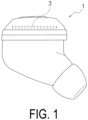
- FIG. 1 is a schematic perspective view of the wireless earbud in which an antenna device according to a first embodiment of the present invention is incorporated.
- the wireless earbud 1 includes an antenna device 3 and the like that are incorporated in a housing.
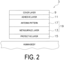
- FIG. 2 is a schematic diagram illustrating a layer configuration of the antenna device.
- a lower side in the drawing is a human body side.
- the antenna device 3 is, for example, Bluetooth (trade name), and includes a cover layer 9, an adhesive layer 11, a metasurface layer 13 (an example of a metasurface layer), and a protective layer 15 from an upper side to the lower side in the drawing.
- the metasurface layer 13 includes one or more low-loss films and metasurfaces (described below).
- An antenna pattern 17 (an example of an antenna) is formed on an upper surface of the metasurface layer 13 in the drawing.
- the metasurface layer 13 is disposed on the human body side with respect to the antenna pattern 17.
- An antenna film 19 is formed of the metasurface layer 13 and the antenna pattern 17 that are described above.
- the cover layer 9 is made of, for example, polycarbonate, and has a thickness of 2 mm.
- the adhesive layer 11 is, for example, OCA, and has a thickness of 25 ⁇ m.
- the antenna pattern 17 is made of, for example, copper, and has a thickness of 3 ⁇ m.
- FIG. 3 is a schematic diagram illustrating a cross-sectional configuration of the antenna film.
- the antenna film 19 includes a first low-loss film 20A, a second low-loss film 20B, and a third low-loss film 20C from the lower side in the drawing.
- the films are layered one another.
- Each of the low-loss films is made of, for example, PET or COP, and has a thickness of 50 to 150 ⁇ m.
- the low-loss film may be made of any material having a low tan ⁇ (low-dielectric loss material) and is not limited to particular materials.
- the total thickness of the low-loss film is preferably 150 ⁇ m or less.
- the antenna pattern 17 is formed on an upper surface of the third low-loss film 20C.
- a first electrode 21A1 of a first metasurface 21A is formed on an upper surface of the first low-loss film 20A.
- a second electrode 21B1 of a second metasurface 21B is formed on an upper surface of the second low-loss film 20B.
- the metasurface is made of, for example, copper, and has a thickness of 3 ⁇ m .
- the metasurface may be formed of a visible light transparent conductive film. Specifically, Indium Tin Oxide (ITO) and transparent conductive ink (for example, silver nanowire ink) are used.
- ITO Indium Tin Oxide
- transparent conductive ink for example, silver nanowire ink
- the metasurface is "a periodic structure shorter than an artificially constructed incident radio wavelength". Electromagnetic field characteristics are determined by a resonance phenomenon of the periodic structure in the metasurface, and appropriately designing the periodic structure allows peculiar electromagnetic field characteristics having a negative refractive index, which cannot be obtained from the natural world, to be obtained.
- a ground 29 is formed on a lower surface of the first low-loss film 20A.
- the ground 29 is a fully formed solid layer.
- the first electrodes 21A1 are disposed at intervals from each other, for example, in a grid. Capacitance components are generated between the intervals. Further, capacitance components are also generated between the first electrodes 21A1 and the ground 29. Furthermore, inductance components are generated in the first electrode 21A1 itself.
- the first metasurface 21A includes a first through-hole 21A2 through which the first electrode 21A1 is connected to the ground 29.
- the second metasurface 21B includes a second through-hole 21B2 through which the second electrode 21B1 is connected to the ground 29.
- the first through-hole 21A2 corresponds to each one of the first electrodes 21A1 and extends through the second low-loss film 20B and the first low-loss film 20A to connect the first electrode 21A1 to the ground 29. Therefore, an inductance component is generated in the first through-hole 21A2.
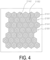
- FIG. 4 is a schematic plan view illustrating a plane position of a metasurface.
- the first electrode 21A1 and the second electrode 21B1 are regular hexagons.
- the first electrodes 21A1 and the second electrodes 21B 1 in respective rows are alternately arranged side by side and are not overlapped with each other in a planar view. Note that the first through-hole 21A2 is provided corresponding to the first electrode 21A1 and that the second through-hole 21B2 is provided corresponding to the second electrode 21B1.
- ECG electromagnetic band gap
- AMC artificial magnetic conductor
- Adopting the EBG structure as described above allows the thickness of the antenna (for example, the thickness of the antenna film 19) of ⁇ /4 or less while maintaining emission efficiency. This is because the periodic structure is well formed in accordance with the target frequency and thus electromagnetic waves incident on the EBG structure can be in phase with reflected electromagnetic waves. In a case where the phase is the same, electromagnetic waves reflected from the EBG structure and electromagnetic waves emitted into the space without being reflected intensify together even when the thickness is not set to ⁇ /4. Therefore, the thickness can be reduced with emission efficiency maintained.
- the first metasurface 21A and the second metasurface 21B are respectively disposed on the first low-loss film 20A and the second low-loss film 20B.
- using thin low-loss films enables the small antenna device to be established.
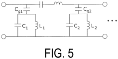
- FIG. 5 is an equivalent circuit diagram of the antenna device.
- Inductance components L 1 and L 2 are respectively generated between the first electrode 21A1 and the first through-hole 21A2 and between the second electrode 21B1 and the second through-hole 21B2. Further, capacitance components C 1 and C 2 are respectively generated between the first electrode 21A1 and the ground 29 and between the second electrode 21B1 and the ground 29. Furthermore, capacitance components C g1 and C g2 are respectively generated between the first electrode 21A1 and the antenna pattern 17 and between the second electrode 21B1 and the antenna pattern 17.
- Forming the first electrode 21A1 and the second electrode 21B 1 on a plurality of layers of the thin first low-loss film 20A and the thin second low-loss film 20B, respectively, as described above allows even thin films to form equivalent circuits (of the EBG structure) in which filters made up of inductance and capacitance are disposed on a periodic basis.
- Adjusting, with simulation, filter characteristics made up of such L and C, the shape and size of the electrode, which is the smallest unit of the periodic structure, the number of repetitions, and the thickness of the plurality of films enables broadband impedance matching, and a reflection coefficient ⁇ can be set to +1.
- energy on the surface can be controlled in view of the filter equivalent circuits, that is, multiple reflection is suppressed by the multi-stage configuration of the metasurfaces disposed on the human body side with respect to the antenna pattern 17, and thus the energy emitted from the antenna pattern 17 to the human body is reduced. Consequently, the reflection of radio waves from the human body can be reduced. As a result, the influence on the antenna pattern 17 is reduced, allowing the radio waves to be sufficiently emitted in the target direction.
- the metasurface may be formed of holes disposed in a two-dimensional square grid (that is, in a matrix) having periodicity in conductive members.
- the shape of the conductive members or the holes is not limited to particular shapes and can be various if the conductive members or the holes can be periodically disposed.
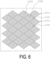
- FIG. 6 is a schematic plan view illustrating a plane position of a metasurface according to the modified example.
- the basic configuration is the same as that in the embodiment described above.
- a third electrode 21C1 and a fourth electrode 21D1 correspond to the first electrode 21A1 and the second electrode 21B1 of the first embodiment and have regular hexagons.
- the third electrodes 21C1 and the fourth electrodes 21D1 in respective rows are alternately arranged side by side and are not overlapped with each other in a planar view. Note that a third through-hole 21C2 is provided corresponding to the third electrode 21C1 and that a fourth through-hole 21D2 is provided corresponding to the fourth electrode 21D1.
- the number of layers of the low-loss films may be three but may be three or more.
- FIG. 7 is a schematic diagram illustrating a cross-sectional configuration of an antenna device according to the second embodiment.
- FIG. 8 is a schematic plan view illustrating plane positions of an antenna and a metasurface in each low-loss film.
- the antenna device 3 is, for example, a plate inverted F antenna (PIFA), and includes the metasurface layer 13.
- PIFA plate inverted F antenna
- the metasurface layer 13 includes a plurality of low-loss films and metasurfaces (described below).
- the antenna pattern 17 is formed on the upper surface of the metasurface layer 13 in the drawing.
- the antenna film 19 is formed of the metasurface layer 13 and the antenna pattern 17 that are described above.
- the antenna film 19 includes the first low-loss film 20A, the second low-loss film 20B, the third low-loss film 20C, and a fourth low-loss film 20D from the lower side in the drawing.
- the films are layered together.
- the antenna pattern 17 is formed on an upper surface of the fourth low-loss film 20D.
- the first electrode 21A1 of the first metasurface 21A is formed on the upper surface of the first low-loss film 20A.
- the second electrode 21B 1 of the second metasurface 21B is formed on the upper surface of the second low-loss film 20B.
- the ground 29 is formed on the lower surface of the first low-loss film 20A.
- the first electrodes 21A1 are disposed at intervals from each other, for example, in a grid. The same applies to the second electrode 21B 1.
- the first metasurface 21A includes the first through-hole 21A2 through which the first electrode 21A1 is connected to the ground 29.
- the second metasurface 21B includes the second through-hole 21B2 through which the second electrode 21B1 is connected to the ground 29.
- the first through-hole 21A2 corresponds to each one of the first electrodes 21A1 and extends through the second low-loss film 20B and the first low-loss film 20A to connect the first electrode 21A1 to the ground 29.
- the number of layers of the low-loss films are three in the first embodiment but may be three or more.
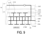
- FIG. 9 is a schematic diagram illustrating a cross-sectional configuration of an antenna device according to the third embodiment.
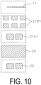
- FIG. 10 is a schematic plan view illustrating plane positions of an antenna and a metasurface in each low-loss film.
- the lower side in the drawing is the human body side.
- the antenna device 3 is, for example, a plate inverted F antenna (PIFA), and includes the metasurface layer 13.
- PIFA plate inverted F antenna
- the metasurface layer 13 includes a plurality of low-loss films and metasurfaces (described below).
- the antenna pattern 17 is formed on the upper surface of the metasurface layer 13 in the drawing.
- the antenna film 19 is formed of the metasurface layer 13 and the antenna pattern 17 that are described above.
- the antenna film 19 includes the first low-loss film 20A, the second low-loss film 20B, the third low-loss film 20C, the fourth low-loss film 20D, and a fifth low-loss film 20E from the lower side in the drawing.
- the films are layered together.
- the antenna pattern 17 is formed on an upper surface of the fifth low-loss film 20E.
- the first electrode 21A1 of the first metasurface 21A is formed on the upper surface of the second low-loss film 20B.
- the second electrode 21B 1 of the second metasurface 21B is formed on the upper surface of the third low-loss film 20C.
- the ground 29 is formed on the upper surface of the first low-loss film 20A.
- Third electrodes 30 are formed on a lower surface of the first low-loss film 20A.
- the first electrodes 21A1 are disposed at intervals from each other, for example, in a grid. The same applies to the second electrode 21B 1.
- the first metasurface 21A includes the first through-hole 21A2 through which the first electrode 21A1, the ground 29, and the third electrode 30 are connected.
- the second metasurface 21B includes the second through-hole 21B2 through which the second electrode 21B1 is connected to the ground 29.
- the first through-hole 21A2 corresponds to each one of the first electrodes 21A1 and each one of the third electrodes 30 and extends through the second low-loss film 20B and the first low-loss film 20A.
- the number of low-loss films on which metasurfaces are formed are two in the first to third embodiments but may be two or more.
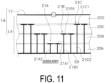
- FIG. 11 is a schematic diagram illustrating a cross-sectional configuration of an antenna device according to the fourth embodiment.
- FIG. 12 is a schematic plan view illustrating plane positions of an antenna and a metasurface in each low-loss film.
- the lower side in the drawing is the human body side.
- the antenna device 3 is, for example, a dipole antenna, and includes the metasurface layer 13.
- the metasurface layer 13 includes a plurality of low-loss films and metasurfaces (described below).
- the antenna pattern 17 is formed on the upper surface of the metasurface layer 13 in the drawing.
- the antenna film 19 is formed of the metasurface layer 13 and the antenna pattern 17 that are described above.
- the antenna film 19 includes the first low-loss film 20A, the second low-loss film 20B, the third low-loss film 20C, and the fourth low-loss film 20D from the lower side in the drawing.
- the films are layered together.
- the antenna pattern 17 is formed on the upper surface of the fourth low-loss film 20D.
- the first electrode 21A1 of the first metasurface 21A is formed on the upper surface of the first low-loss film 20A.
- the second electrode 21B 1 of the second metasurface 21B is formed on the upper surface of the second low-loss film 20B.
- the third electrodes 21C1 of the third metasurface 21C are formed on the upper surface of the third low-loss film 20C.
- the ground 29 is formed on the lower surface of the first low-loss film 20A.
- the first electrodes 21A1 are disposed at intervals from each other in a grid. The same applies to the second electrode 21B 1 and the third electrode 21C1.
- the first metasurface 21A includes the first through-hole 21A2 through which the first electrode 21A1 is connected to the ground 29.
- the second metasurface 21B includes the second through-hole 21B2 through which the second electrode 21B1 is connected to the ground 29.
- the third metasurface 21C includes a third through-hole 21C2 through which the third electrode 21C1 is connected to the ground 29.
- the first through-hole 21A2 corresponds to each one of the first electrodes 21A1 and extends through the first low-loss film 20A to connect the first electrode 21A1 to the ground 29.
- the electrode of the metasurface is connected via the through-hole to the ground; however, by increasing the area of the electrode or decreasing an interval between the layers, the through-hole for the electrode may be omitted.
- FIG. 13 is a schematic diagram illustrating a cross-sectional configuration of an antenna device according to the fifth embodiment.
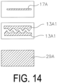
- FIG. 14 is a schematic plan view illustrating plane positions of an antenna and a metasurface in each low-loss film.
- the antenna device 3 is, for example, a plate inverted F antenna (PIFA), and includes a metasurface layer 13A.
- PIFA plate inverted F antenna
- the metasurface layer 13A includes a plurality of low-loss films and metasurfaces (described below).
- An antenna pattern 17A is formed on an upper surface of the metasurface layer 13A in the drawing.
- An antenna film 19A is formed of the metasurface layer 13A and the antenna pattern 17A that are described above.
- the antenna film 19A includes a first low-loss film 22A, a second low-loss film 22B, and a third low-loss film 22C from the lower side in the drawing.
- the films are layered together.
- the antenna pattern 17A is formed on an upper surface of the third low-loss film 22C.
- Electrodes 13A1 of the metasurface are formed below the second low-loss film 20B.
- the electrodes 13A1 include, for example, as illustrated in FIG. 14 , a combination of a pair of electrodes extending in one direction while being disposed side by side. More specifically, the pair of electrodes of the electrodes 13A1 include triangular projections extending toward each other and leave a portion where a zigzag-shaped (sawtooth-shaped) electrode is not formed between the pair of electrodes.
- a ground 29A is formed on a lower surface of the first low-loss film 22A. As described above, only the first low-loss film 22A is disposed between the electrodes 13A1 of the metasurface and the ground 29A.
- the antenna performance is maintained by one or a plurality of features such as the wide shape of the electrode, the short distance between the electrode and the ground, and the like.
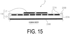
- FIG. 15 is a schematic diagram illustrating a cross-sectional configuration of an antenna device according to the sixth embodiment.
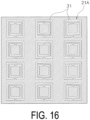
- FIG. 16 is a schematic plan view illustrating a plane position of a metasurface.
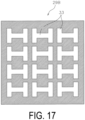
- FIG. 17 is a schematic plan view illustrating a planar configuration of a ground.
- the lower side in the drawing is the human body side.
- the antenna device 3 includes the metasurface layer 13.
- the metasurface layer 13 includes a plurality of low-loss films and metasurfaces (described below).
- the antenna pattern 17 is formed on the upper surface of the metasurface layer 13 in the drawing.
- the antenna film 19 is formed of the metasurface layer 13 and the antenna pattern 17 that are described above.
- the antenna film 19 includes the first low-loss film 20A, the second low-loss film 20B from the lower side in the drawing.
- the films are layered together.
- the antenna pattern 17 is formed on the upper surface of the second low-loss film 20B.
- the first metasurface 21A is formed on the upper surface of the first low-loss film 20A. As illustrated in FIG. 16 , the first metasurface 21A is a complementary split ring resonator (CSRR) and includes cutouts 31 having a split ring shape.
- CSRR complementary split ring resonator
- a ground 29B is formed on the lower side of the first low-loss film 20A.
- the ground 29B is a defect ground structure (DGS) in which cutouts 33 corresponding to the first metasurface 21A are formed.
- the cutouts 33 are each formed in an H-shape.
- the antenna film 19 without through-holes is implemented.
- the metasurface which is one layer, can further achieve a multi-stage equivalent circuit as in the first embodiment.
- FIG. 18 is a schematic plan view illustrating plane positions of an antenna and a metasurface in each low-loss film according to the seventh embodiment.
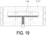
- FIG. 19 is a schematic plan view of a metasurface according to a modified example.
- the layer configuration of the seventh embodiment is the same as that of the fifth embodiment.
- the metasurface is one layer.
- the antenna pattern 17A has a linear shape extending in one direction.
- the power supply of the antenna pattern 17A is performed at the intermediate position in whole.
- the first electrode 21A1 of the first metasurface 21A has an H-shape in a planar view.
- an antenna pattern 17B is a co-planar wave-line (CPW) path structure, and the power supply to the antenna is performed at a lower end of the CPW.
- CPW co-planar wave-line
- FIG. 20 is a schematic plan view of a metasurface according to the eighth embodiment.
- electrodes 41 of a metasurface 21 have a fractal shape.
- the fractal refers to one in which a diagram portion and the entire portion are self-similar (recursion).
- the electrodes 41 of the metasurface 21 each have the shape formed of a large number of self-similar rectangles.
- the minimum unit of the electrode 41 is a rectangular conductive member, and the conductive member includes a rectangular portion in the center in which a conductive member is not formed.
- the electrodes of the metasurface adopt the fractal shape as described above, it can be easy to provide broadband and miniaturization. In particular, broadband characteristics can be obtained as the fractal order increases.
- the electrode of the metasurface having a fractal shape as in the present embodiment allows various equivalent circuits to be created, allowing the entire size to be reduced while maintaining performance. This allows through-holes to be omitted.
- the metasurface includes one layer but may include multiple layers. In the case of the multiple layers, through-holes may be provided or may be omitted.
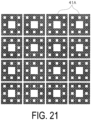
- FIG. 21 is a schematic plan view illustrating a metasurface according to the ninth embodiment.
- electrodes 41A of the metasurface 21 have a fractal shape. Specifically, the electrodes 41A of the metasurface 21 each have the shape formed of a large number of self-similar rectangles.
- the electrode 41A is an example in which the fractal order is greater than that of the electrode 41.
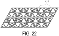
- FIG. 22 is a schematic plan view of a metasurface according to the tenth embodiment.
- electrodes 41B of the metasurface 21 have a fractal shape.
- the electrodes 41B are each a graphic formed of an infinite number of self-similar triangles. Note that the minimum unit of the electrode 41B is a triangular conductive member, and a reversed triangular portion in which a conductive member is not formed is present between the three conductive members oriented in the same direction.
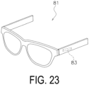
- FIG. 23 is a schematic perspective view of smart glasses in which an antenna device according to the eleventh embodiment is incorporated.
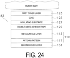
- FIG. 24 is a schematic diagram illustrating a layer configuration of the antenna device.
- smart glasses 81 internally include an antenna device 83.
- the antenna device 83 is, for example, Bluetooth (trade name), and includes a first cover layer 123, a GND 125, an insulating substrate 127, double-sided adhesive tape 129, a metasurface layer 113 (an example of the metasurface layer), and a second cover layer 131 from the upper side toward the lower side in the drawing.
- Bluetooth trademark
- the antenna device 83 includes a first cover layer 123, a GND 125, an insulating substrate 127, double-sided adhesive tape 129, a metasurface layer 113 (an example of the metasurface layer), and a second cover layer 131 from the upper side toward the lower side in the drawing.
- the metasurface layer 113 includes one or a plurality of low-loss films and metasurfaces (described below).
- An antenna pattern 117 is formed on a lower surface of the metasurface layer 113 in the drawing.
- the metasurface layer 113 is disposed on the human body side with respect to the antenna pattern 117.
- An antenna film 119 is formed of the metasurface layer 113 and the antenna pattern 117 that are described above.
- the configuration of the metasurface layer 113 is the same as those of the metasurface layers according to the first to tenth embodiments.
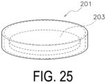
- FIG. 25 is a schematic perspective view of a continuous glucose monitoring in which an antenna device according to the twelfth embodiment is incorporated.
- FIG. 26 is a schematic diagram illustrating a cross-sectional configuration of the antenna device.
- FIG. 27 is a schematic perspective view of the antenna device.
- FIG. 28 is a schematic plan view of the antenna device.
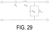
- FIG. 29 is an equivalent circuit diagram of the antenna device.
- a continuous glucose monitoring (GMC) 201 is mounted on a person's arm, and a measurement result is displayed, for example, on a display device (not illustrated).
- the GMC 201 includes an antenna device 203.
- the antenna device 203 is, for example, a dipole antenna, and includes an antenna film 205 as illustrated in FIG. 26 .
- the antenna film 205 includes a first low-loss film 207, a second low-loss film 209, and a third low-loss film 211 from the lower side toward the upper side in the drawing.
- the films are layered together.
- the antenna film 205 includes a ground 221 formed on a lower surface of the first low-loss film 207.
- the antenna film 205 includes a first conductor pattern 213 formed on an upper surface of the first low-loss film 207.
- the first conductor pattern 213 is a circular shape in a planar view.
- a first through-hole 215 extends from the first conductor pattern 213 to the ground 221. The first through-hole 215 configures an antenna feed.
- the antenna film 205 includes a second conductor pattern 217 formed on an upper surface of the second low-loss film 209.
- the second conductor pattern 217 is a circular shape in a planar view.
- the second conductor pattern 217 is larger in area than the first conductor pattern 213 and covers the first conductor pattern 213 in a planar view.
- a plurality of second through-holes 219 extends from the second conductor pattern 217 to the ground 221.
- the second through-holes 219 are disposed around the first conductor pattern 213.
- a capacitance component C L is generated between the first conductor pattern 213 and the second conductor pattern 217.
- a capacitance component C R is generated between the second conductor pattern 217 and the ground 221.
- An inductance component L R is generated in the second conductor pattern 217.
- An inductance component L L is generated in the second through-holes 219.
- this embodiment provides four of the second through-holes 219 disposed at equal intervals in a circumferential direction, that is, with periodicity.
- ZOR zero order resonance
- the number of second through-holes is not limited.
- the present invention is widely applicable to an antenna device used at or near a human body or other conductor.
Landscapes
- Physics & Mathematics (AREA)
- Optics & Photonics (AREA)
- Details Of Aerials (AREA)
- Aerials With Secondary Devices (AREA)
Description
- The present invention relates to an antenna device and particularly to an antenna device to be used at or near a human body or other conductors.
- In recent years, various types such as watch type, spectacle type, ring type, shoe type, pocket type, and pendant type of wearable computers have been developed.
- Electronic devices such as earphones and headphones to be used in close contact with a human body have also been already used. Furthermore, electronic devices such as mobile phones and smart phones are obviously used in close contact with or close to a human body.
- Various types of antennas for performing communication are incorporated in the electronic devices described above (for example, see Patent Document 1).
-
US 2008/0129511 A1 describes an RFID chip attached to an antenna. The RFID chip and the antenna are mounted to an electromagnetic band gap structure. The antenna includes metal patches vias and two layers of dielectric material. - SAKTHI ABIRAMI BALAKRISHNAN ET AL dealt with a conformal self-balanced EBG integrated printed folded dipole antenna for wireless body area networks ("Conformal self-balanced EBG integrated printed folded dipole antenna for wireless body area networks", IET MICROWAVES, ANTENNAS & PROPAGATION, THE INSTITUTION OF ENGINEERING AND TECHNOLOGY, UNITED KINGDOM, vol. 13, no. 14, 14 August 2019, pages 2480-2485). The antenna is printed on a polyester film of a thickness of 0.1 mm as substrate and has a dipole length of λ/4 < 1 < λ. A unit cell is generated by adding squares on all the four comers of the primitive unit cell. In iterations, smaller squares are added subsequently.
- AGARWAL KUSH ET AL dealt with a wearable antenna device comprising a Yagi-Uda antenna and a multilayered periodic metasurface printed on latex substrates having two overlapping AMC layers ("Wearable AMC Backed Near-Endfire Antenna for On-Body Communications on Latex Substrate", IEEE TRANSACTIONS ON COMPONENTS, PACKAGING AND MANUFACTURING TECHNOLOGY, IEEE, USA, vol. 6, no. 3, 10 February 2016, pages 346-358).
- The inventors of the present application have focused on the fact that using a known electronic device with an antenna in close contact with or at or near a human body (head or hand) causes the following problem.
- The problem is that radio waves emitted from the antenna are reflected on the human body, and thus emission characteristics of the antenna are distorted. In this case, the radio waves are not sufficiently emitted from the antenna in the target direction.
- An object of the present invention is to suppress reflection from a human body or other conductors in an antenna device and thereby allow radio waves to be sufficiently emitted in the target direction.
- Some aspects will be described below as means to solve the problems.
- An antenna device according to an aspect of the present invention configured to be used in contact with or close to a human body or a conductor is provided by
claim 1. - The metasurface layer is a layer that is layered on the antenna and disposed on a human body side. The metasurface layer includes a low-loss film and a metasurface formed on the low-loss film.
- In the device, the metasurface layer is disposed on the human body side of the antenna. Accordingly, the metasurface layer suppresses reflection of electromagnetic waves from the human body side, allowing the influence on the antenna to be reduced. As a result, radio waves are sufficiently emitted in the target direction.
- In the device, the metasurface is disposed on the low-loss film. In this case, using the thin low-loss film allows the small antenna device to be implemented.
- A plurality of the low-loss films may be used.
- The metasurface may be formed on each of the plurality of the low-loss films.
- The device forms the metasurfaces on the low-loss films in a multi-layer, allowing even the thin low-loss film to configure a filter equivalent circuit that suppresses multiple reflection with a multi-stage circuit configuration. This enables impedance matching.
- The low-loss film may have a thickness of 150 µm or less.
- The metasurface may have a fractal shape.
- In the device, increasing the fractal order of the metasurface allows broadband characteristics to be easily achieved.
- An antenna device according to the present invention suppresses reflection from the human body, allowing radio waves to be sufficiently emitted in the target direction.
-
-
FIG. 1 is a schematic perspective view of a wireless earbud in which an antenna device according to a first embodiment of the present invention is incorporated. -
FIG. 2 is a schematic diagram illustrating a layer configuration of the antenna device. -
FIG. 3 is a schematic diagram illustrating a cross-sectional configuration of an antenna film. -
FIG. 4 is a schematic plan view illustrating a plane position of a metasurface. -
FIG. 5 is an equivalent circuit diagram of the antenna device. -
FIG. 6 is a schematic plan view illustrating a plane position of a metasurface according to a modified example. -
FIG. 7 is a schematic diagram illustrating a cross-sectional configuration of an antenna device according to a second embodiment of the present invention. -
FIG. 8 is a schematic plan view illustrating plane positions of an antenna and a metasurface in each low-loss film. -
FIG. 9 is a schematic diagram illustrating a cross-sectional configuration of an antenna device according to a third embodiment of the present invention. -
FIG. 10 is a schematic plan view illustrating plane positions of an antenna and a metasurface in each low-loss film. -
FIG. 11 is a schematic diagram illustrating a cross-sectional configuration of an antenna device according to a fourth embodiment of the present invention. -
FIG. 12 is a schematic plan view illustrating plane positions of an antenna and a metasurface in each low-loss film. -
FIG. 13 is a schematic diagram illustrating a cross-sectional configuration of an antenna device according to a fifth embodiment of the present invention. -
FIG. 14 is a schematic plan view illustrating a plane position of a metasurface. -
FIG. 15 is a schematic diagram illustrating a cross-sectional configuration of an antenna device according to a sixth embodiment of the present invention. -
FIG. 16 is a schematic plan view illustrating a plane position of a metasurface. -
FIG. 17 is a schematic diagram illustrating a planar configuration of a ground. -
FIG. 18 is a schematic plan view illustrating plane positions of an antenna and a metasurface in each low-loss film according to a seventh embodiment of the present invention. -
FIG. 19 is a schematic plan view of a metasurface according to a modified example. -
FIG. 20 is a schematic plan view of a metasurface according to an eighth embodiment of the present invention. -
FIG. 21 is a schematic plan view of a metasurface according to a ninth embodiment of the present invention. -
FIG. 22 is a schematic plan view of a metasurface according to a tenth embodiment of the present invention. -
FIG. 23 is a schematic perspective view of smart glasses in which an antenna device according to an eleventh embodiment of the present invention is incorporated. -
FIG. 24 is a schematic diagram illustrating a layer configuration of the antenna device. -
FIG. 25 is a drawing illustrating a use state of a continuous glucose monitoring in which an antenna device according to a twelfth embodiment of the present invention is incorporated. A schematic perspective view of the continuous glucose monitoring. -
FIG. 26 is a schematic diagram illustrating a cross-sectional configuration of the antenna device. -
FIG. 27 is a schematic perspective view of the antenna device. -
FIG. 28 is a schematic plan view of the antenna device. -
FIG. 29 is an equivalent circuit diagram of the antenna device. - A
wireless earbud 1 will be described with the use ofFIG. 1. FIG. 1 is a schematic perspective view of the wireless earbud in which an antenna device according to a first embodiment of the present invention is incorporated. - The
wireless earbud 1 includes anantenna device 3 and the like that are incorporated in a housing. - The
antenna device 3 will be described with the use ofFIG. 2. FIG. 2 is a schematic diagram illustrating a layer configuration of the antenna device. - In
FIG. 2 , a lower side in the drawing is a human body side. Theantenna device 3 is, for example, Bluetooth (trade name), and includes a cover layer 9, anadhesive layer 11, a metasurface layer 13 (an example of a metasurface layer), and aprotective layer 15 from an upper side to the lower side in the drawing. - The
metasurface layer 13 includes one or more low-loss films and metasurfaces (described below). An antenna pattern 17 (an example of an antenna) is formed on an upper surface of themetasurface layer 13 in the drawing. Themetasurface layer 13 is disposed on the human body side with respect to theantenna pattern 17. Anantenna film 19 is formed of themetasurface layer 13 and theantenna pattern 17 that are described above. - The cover layer 9 is made of, for example, polycarbonate, and has a thickness of 2 mm. The
adhesive layer 11 is, for example, OCA, and has a thickness of 25 µm. Theantenna pattern 17 is made of, for example, copper, and has a thickness of 3 µm. - The
antenna film 19 will be described with the use ofFIG. 3. FIG. 3 is a schematic diagram illustrating a cross-sectional configuration of the antenna film. - The
antenna film 19 includes a first low-loss film 20A, a second low-loss film 20B, and a third low-loss film 20C from the lower side in the drawing. The films are layered one another. Each of the low-loss films is made of, for example, PET or COP, and has a thickness of 50 to 150 µm. The low-loss film may be made of any material having a low tan δ (low-dielectric loss material) and is not limited to particular materials. The total thickness of the low-loss film is preferably 150 µm or less. - The
antenna pattern 17 is formed on an upper surface of the third low-loss film 20C. - A first electrode 21A1 of a
first metasurface 21A is formed on an upper surface of the first low-loss film 20A. A second electrode 21B1 of asecond metasurface 21B is formed on an upper surface of the second low-loss film 20B. The metasurface is made of, for example, copper, and has a thickness of 3 µm . Also, the metasurface may be formed of a visible light transparent conductive film. Specifically, Indium Tin Oxide (ITO) and transparent conductive ink (for example, silver nanowire ink) are used. - Note that the metasurface is "a periodic structure shorter than an artificially constructed incident radio wavelength". Electromagnetic field characteristics are determined by a resonance phenomenon of the periodic structure in the metasurface, and appropriately designing the periodic structure allows peculiar electromagnetic field characteristics having a negative refractive index, which cannot be obtained from the natural world, to be obtained.
- A
ground 29 is formed on a lower surface of the first low-loss film 20A. Theground 29 is a fully formed solid layer. - The first electrodes 21A1 are disposed at intervals from each other, for example, in a grid. Capacitance components are generated between the intervals. Further, capacitance components are also generated between the first electrodes 21A1 and the
ground 29. Furthermore, inductance components are generated in the first electrode 21A1 itself. - The same applies to the second electrode 21B1.
- The
first metasurface 21A includes a first through-hole 21A2 through which the first electrode 21A1 is connected to theground 29. - The
second metasurface 21B includes a second through-hole 21B2 through which the second electrode 21B1 is connected to theground 29. - The first through-hole 21A2 corresponds to each one of the first electrodes 21A1 and extends through the second low-
loss film 20B and the first low-loss film 20A to connect the first electrode 21A1 to theground 29. Therefore, an inductance component is generated in the first through-hole 21A2. - The same applies to the second through-hole 21B2.
- The pattern arrangement of the first metasurface and the second metasurface will be described with the use of
FIG. 4. FIG. 4 is a schematic plan view illustrating a plane position of a metasurface. - The first electrode 21A1 and the second electrode 21B1 are regular hexagons. The first electrodes 21A1 and the
second electrodes 21B - The structure described above allows an electromagnetic band gap (EBG) or artificial magnetic conductor (AMC) structure to be implemented.
- Adopting the EBG structure as described above allows the thickness of the antenna (for example, the thickness of the antenna film 19) of λ/4 or less while maintaining emission efficiency. This is because the periodic structure is well formed in accordance with the target frequency and thus electromagnetic waves incident on the EBG structure can be in phase with reflected electromagnetic waves. In a case where the phase is the same, electromagnetic waves reflected from the EBG structure and electromagnetic waves emitted into the space without being reflected intensify together even when the thickness is not set to λ/4. Therefore, the thickness can be reduced with emission efficiency maintained.
- As described above, the
first metasurface 21A and thesecond metasurface 21B are respectively disposed on the first low-loss film 20A and the second low-loss film 20B. In this case, using thin low-loss films enables the small antenna device to be established. - An equivalent circuit of the antenna device will be described with the use of
FIG. 5. FIG. 5 is an equivalent circuit diagram of the antenna device. - Inductance components L1 and L2 are respectively generated between the first electrode 21A1 and the first through-hole 21A2 and between the second electrode 21B1 and the second through-hole 21B2. Further, capacitance components C1 and C2 are respectively generated between the first electrode 21A1 and the
ground 29 and between the second electrode 21B1 and theground 29. Furthermore, capacitance components Cg1 and Cg2 are respectively generated between the first electrode 21A1 and theantenna pattern 17 and between the second electrode 21B1 and theantenna pattern 17. - Forming the first electrode 21A1 and the
second electrode 21Bloss film 20A and the thin second low-loss film 20B, respectively, as described above allows even thin films to form equivalent circuits (of the EBG structure) in which filters made up of inductance and capacitance are disposed on a periodic basis. - Adjusting, with simulation, filter characteristics made up of such L and C, the shape and size of the electrode, which is the smallest unit of the periodic structure, the number of repetitions, and the thickness of the plurality of films enables broadband impedance matching, and a reflection coefficient Γ can be set to +1.
- In other words, energy on the surface can be controlled in view of the filter equivalent circuits, that is, multiple reflection is suppressed by the multi-stage configuration of the metasurfaces disposed on the human body side with respect to the
antenna pattern 17, and thus the energy emitted from theantenna pattern 17 to the human body is reduced. Consequently, the reflection of radio waves from the human body can be reduced. As a result, the influence on theantenna pattern 17 is reduced, allowing the radio waves to be sufficiently emitted in the target direction. - Note that the metasurface may be formed of holes disposed in a two-dimensional square grid (that is, in a matrix) having periodicity in conductive members. Also, the shape of the conductive members or the holes is not limited to particular shapes and can be various if the conductive members or the holes can be periodically disposed.
- A modified example of the metasurface in a shape in a planar view will be described with the use of
FIG. 6. FIG. 6 is a schematic plan view illustrating a plane position of a metasurface according to the modified example. The basic configuration is the same as that in the embodiment described above. - A third electrode 21C1 and a fourth electrode 21D1 correspond to the first electrode 21A1 and the second electrode 21B1 of the first embodiment and have regular hexagons. The third electrodes 21C1 and the fourth electrodes 21D1 in respective rows are alternately arranged side by side and are not overlapped with each other in a planar view. Note that a third through-hole 21C2 is provided corresponding to the third electrode 21C1 and that a fourth through-hole 21D2 is provided corresponding to the fourth electrode 21D1.
- In the first embodiment, the number of layers of the low-loss films may be three but may be three or more.
- A second embodiment of the present invention will be described as such an embodiment with the use of
FIGS. 7 and8 .FIG. 7 is a schematic diagram illustrating a cross-sectional configuration of an antenna device according to the second embodiment.FIG. 8 is a schematic plan view illustrating plane positions of an antenna and a metasurface in each low-loss film. - The
antenna device 3 is, for example, a plate inverted F antenna (PIFA), and includes themetasurface layer 13. - The
metasurface layer 13 includes a plurality of low-loss films and metasurfaces (described below). Theantenna pattern 17 is formed on the upper surface of themetasurface layer 13 in the drawing. Theantenna film 19 is formed of themetasurface layer 13 and theantenna pattern 17 that are described above. - The
antenna film 19 includes the first low-loss film 20A, the second low-loss film 20B, the third low-loss film 20C, and a fourth low-loss film 20D from the lower side in the drawing. The films are layered together. - The
antenna pattern 17 is formed on an upper surface of the fourth low-loss film 20D. - The first electrode 21A1 of the
first metasurface 21A is formed on the upper surface of the first low-loss film 20A. Thesecond electrode 21Bsecond metasurface 21B is formed on the upper surface of the second low-loss film 20B. - The
ground 29 is formed on the lower surface of the first low-loss film 20A. - The first electrodes 21A1 are disposed at intervals from each other, for example, in a grid. The same applies to the
second electrode 21B - The
first metasurface 21A includes the first through-hole 21A2 through which the first electrode 21A1 is connected to theground 29. - The
second metasurface 21B includes the second through-hole 21B2 through which the second electrode 21B1 is connected to theground 29. - The first through-hole 21A2 corresponds to each one of the first electrodes 21A1 and extends through the second low-
loss film 20B and the first low-loss film 20A to connect the first electrode 21A1 to theground 29. - The same applies to the second through-hole 21B2.
- The number of layers of the low-loss films are three in the first embodiment but may be three or more.
- A third embodiment of the present invention will be described as such an embodiment with the use of
FIGS. 9 and10 .FIG. 9 is a schematic diagram illustrating a cross-sectional configuration of an antenna device according to the third embodiment.FIG. 10 is a schematic plan view illustrating plane positions of an antenna and a metasurface in each low-loss film. - In
FIG. 9 , the lower side in the drawing is the human body side. Theantenna device 3 is, for example, a plate inverted F antenna (PIFA), and includes themetasurface layer 13. - The
metasurface layer 13 includes a plurality of low-loss films and metasurfaces (described below). Theantenna pattern 17 is formed on the upper surface of themetasurface layer 13 in the drawing. Theantenna film 19 is formed of themetasurface layer 13 and theantenna pattern 17 that are described above. - In
FIG. 9 , theantenna film 19 includes the first low-loss film 20A, the second low-loss film 20B, the third low-loss film 20C, the fourth low-loss film 20D, and a fifth low-loss film 20E from the lower side in the drawing. The films are layered together. - The
antenna pattern 17 is formed on an upper surface of the fifth low-loss film 20E. - The first electrode 21A1 of the
first metasurface 21A is formed on the upper surface of the second low-loss film 20B. Thesecond electrode 21Bsecond metasurface 21B is formed on the upper surface of the third low-loss film 20C. - The
ground 29 is formed on the upper surface of the first low-loss film 20A. -
Third electrodes 30 are formed on a lower surface of the first low-loss film 20A. - The first electrodes 21A1 are disposed at intervals from each other, for example, in a grid. The same applies to the
second electrode 21B - The
first metasurface 21A includes the first through-hole 21A2 through which the first electrode 21A1, theground 29, and thethird electrode 30 are connected. - The
second metasurface 21B includes the second through-hole 21B2 through which the second electrode 21B1 is connected to theground 29. - The first through-hole 21A2 corresponds to each one of the first electrodes 21A1 and each one of the
third electrodes 30 and extends through the second low-loss film 20B and the first low-loss film 20A. - The same applies to the second through-hole 21B2.
- The number of low-loss films on which metasurfaces are formed are two in the first to third embodiments but may be two or more.
- A fourth embodiment of the present invention will be described as such an embodiment with the use of
FIGS. 11 and12 .FIG. 11 is a schematic diagram illustrating a cross-sectional configuration of an antenna device according to the fourth embodiment.FIG. 12 is a schematic plan view illustrating plane positions of an antenna and a metasurface in each low-loss film. - In
FIG. 11 , the lower side in the drawing is the human body side. Theantenna device 3 is, for example, a dipole antenna, and includes themetasurface layer 13. - The
metasurface layer 13 includes a plurality of low-loss films and metasurfaces (described below). Theantenna pattern 17 is formed on the upper surface of themetasurface layer 13 in the drawing. Theantenna film 19 is formed of themetasurface layer 13 and theantenna pattern 17 that are described above. - In
FIG. 11 , theantenna film 19 includes the first low-loss film 20A, the second low-loss film 20B, the third low-loss film 20C, and the fourth low-loss film 20D from the lower side in the drawing. The films are layered together. - The
antenna pattern 17 is formed on the upper surface of the fourth low-loss film 20D. - The first electrode 21A1 of the
first metasurface 21A is formed on the upper surface of the first low-loss film 20A. Thesecond electrode 21Bsecond metasurface 21B is formed on the upper surface of the second low-loss film 20B. The third electrodes 21C1 of thethird metasurface 21C are formed on the upper surface of the third low-loss film 20C. - The
ground 29 is formed on the lower surface of the first low-loss film 20A. - The first electrodes 21A1 are disposed at intervals from each other in a grid. The same applies to the
second electrode 21B - The
first metasurface 21A includes the first through-hole 21A2 through which the first electrode 21A1 is connected to theground 29. - The
second metasurface 21B includes the second through-hole 21B2 through which the second electrode 21B1 is connected to theground 29. - The
third metasurface 21C includes a third through-hole 21C2 through which the third electrode 21C1 is connected to theground 29. - The first through-hole 21A2 corresponds to each one of the first electrodes 21A1 and extends through the first low-
loss film 20A to connect the first electrode 21A1 to theground 29. - The same applies to the second through-hole 21B2 and the third through-hole 21C2.
- In first to fourth embodiments, the electrode of the metasurface is connected via the through-hole to the ground; however, by increasing the area of the electrode or decreasing an interval between the layers, the through-hole for the electrode may be omitted.
- A fifth embodiment of the present invention will be described as such an embodiment with the use of
FIGS. 13 and14 .FIG. 13 is a schematic diagram illustrating a cross-sectional configuration of an antenna device according to the fifth embodiment.FIG. 14 is a schematic plan view illustrating plane positions of an antenna and a metasurface in each low-loss film. - The
antenna device 3 is, for example, a plate inverted F antenna (PIFA), and includes ametasurface layer 13A. - The
metasurface layer 13A includes a plurality of low-loss films and metasurfaces (described below). Anantenna pattern 17A is formed on an upper surface of themetasurface layer 13A in the drawing. Anantenna film 19A is formed of themetasurface layer 13A and theantenna pattern 17A that are described above. - The
antenna film 19A includes a first low-loss film 22A, a second low-loss film 22B, and a third low-loss film 22C from the lower side in the drawing. The films are layered together. - The
antenna pattern 17A is formed on an upper surface of the third low-loss film 22C. - Electrodes 13A1 of the metasurface are formed below the second low-
loss film 20B. The electrodes 13A1 include, for example, as illustrated inFIG. 14 , a combination of a pair of electrodes extending in one direction while being disposed side by side. More specifically, the pair of electrodes of the electrodes 13A1 include triangular projections extending toward each other and leave a portion where a zigzag-shaped (sawtooth-shaped) electrode is not formed between the pair of electrodes. - A
ground 29A is formed on a lower surface of the first low-loss film 22A. As described above, only the first low-loss film 22A is disposed between the electrodes 13A1 of the metasurface and theground 29A. - In this embodiment, no through-hole that connects the electrode to the ground is formed. However, for example, the antenna performance is maintained by one or a plurality of features such as the wide shape of the electrode, the short distance between the electrode and the ground, and the like.
- Other embodiments in which the metasurface without through-holes will be described.
- A sixth embodiment of the present invention will be described as such an embodiment with the use of
FIGS. 15 to 17 .FIG. 15 is a schematic diagram illustrating a cross-sectional configuration of an antenna device according to the sixth embodiment.FIG. 16 is a schematic plan view illustrating a plane position of a metasurface.FIG. 17 is a schematic plan view illustrating a planar configuration of a ground. - In
FIG. 15 , the lower side in the drawing is the human body side. Theantenna device 3 includes themetasurface layer 13. - The
metasurface layer 13 includes a plurality of low-loss films and metasurfaces (described below). Theantenna pattern 17 is formed on the upper surface of themetasurface layer 13 in the drawing. Theantenna film 19 is formed of themetasurface layer 13 and theantenna pattern 17 that are described above. - In
FIG. 15 , theantenna film 19 includes the first low-loss film 20A, the second low-loss film 20B from the lower side in the drawing. The films are layered together. - The
antenna pattern 17 is formed on the upper surface of the second low-loss film 20B. - The
first metasurface 21A is formed on the upper surface of the first low-loss film 20A. As illustrated inFIG. 16 , thefirst metasurface 21A is a complementary split ring resonator (CSRR) and includescutouts 31 having a split ring shape. - A
ground 29B is formed on the lower side of the first low-loss film 20A. - As illustrated in
FIG. 17 , theground 29B is a defect ground structure (DGS) in which cutouts 33 corresponding to thefirst metasurface 21A are formed. The cutouts 33 are each formed in an H-shape. - As described above, the
antenna film 19 without through-holes is implemented. - As described above, the metasurface, which is one layer, can further achieve a multi-stage equivalent circuit as in the first embodiment.
- A seventh embodiment of the present invention will be described with the use of
FIGS. 18 and19 .FIG. 18 is a schematic plan view illustrating plane positions of an antenna and a metasurface in each low-loss film according to the seventh embodiment.FIG. 19 is a schematic plan view of a metasurface according to a modified example. - The layer configuration of the seventh embodiment is the same as that of the fifth embodiment. In other words, the metasurface is one layer.
- The
antenna pattern 17A has a linear shape extending in one direction. The power supply of theantenna pattern 17A is performed at the intermediate position in whole. - The first electrode 21A1 of the
first metasurface 21A has an H-shape in a planar view. - As described above, an artificial magnetic conductor (AMC) is implemented. Therefore, emission efficiency and impedance matching can be maintained through the reflection coefficient Γ = +1 characteristics. As a result, the impact on the human body can be minimized.
- In the modified example illustrated in
FIG. 19 , anantenna pattern 17B is a co-planar wave-line (CPW) path structure, and the power supply to the antenna is performed at a lower end of the CPW. - An eighth embodiment of the present invention will be described with the use of
FIG. 20. FIG. 20 is a schematic plan view of a metasurface according to the eighth embodiment. - In this embodiment,
electrodes 41 of a metasurface 21 have a fractal shape. The fractal refers to one in which a diagram portion and the entire portion are self-similar (recursion). - Specifically, the
electrodes 41 of the metasurface 21 each have the shape formed of a large number of self-similar rectangles. Note that the minimum unit of theelectrode 41 is a rectangular conductive member, and the conductive member includes a rectangular portion in the center in which a conductive member is not formed. - Since the electrodes of the metasurface adopt the fractal shape as described above, it can be easy to provide broadband and miniaturization. In particular, broadband characteristics can be obtained as the fractal order increases.
- In the related art, it has been considered to omit through-holes from the metasurface due to manufacturing problems. In that case, unfortunately, the metasurface area and the entire area increase to have the same performance.
- The electrode of the metasurface having a fractal shape as in the present embodiment allows various equivalent circuits to be created, allowing the entire size to be reduced while maintaining performance. This allows through-holes to be omitted.
- In this embodiment, the metasurface includes one layer but may include multiple layers. In the case of the multiple layers, through-holes may be provided or may be omitted.
- A ninth embodiment of the present invention will be described with the use of
FIG. 21. FIG. 21 is a schematic plan view illustrating a metasurface according to the ninth embodiment. - In this embodiment,
electrodes 41A of the metasurface 21 have a fractal shape. Specifically, theelectrodes 41A of the metasurface 21 each have the shape formed of a large number of self-similar rectangles. Theelectrode 41A is an example in which the fractal order is greater than that of theelectrode 41. - A tenth embodiment of the present invention will be described with the use of
FIG. 22. FIG. 22 is a schematic plan view of a metasurface according to the tenth embodiment. - In this embodiment,
electrodes 41B of the metasurface 21 have a fractal shape. Specifically, theelectrodes 41B are each a graphic formed of an infinite number of self-similar triangles. Note that the minimum unit of theelectrode 41B is a triangular conductive member, and a reversed triangular portion in which a conductive member is not formed is present between the three conductive members oriented in the same direction. - An eleventh embodiment of the present invention will be described with the use of
FIGS. 23 and24 .FIG. 23 is a schematic perspective view of smart glasses in which an antenna device according to the eleventh embodiment is incorporated.FIG. 24 is a schematic diagram illustrating a layer configuration of the antenna device. - As illustrated in
FIG. 23 ,smart glasses 81 internally include anantenna device 83. - In
FIG. 24 , the lower side in the drawing is the human body side. Theantenna device 83 is, for example, Bluetooth (trade name), and includes afirst cover layer 123, aGND 125, an insulatingsubstrate 127, double-sidedadhesive tape 129, a metasurface layer 113 (an example of the metasurface layer), and asecond cover layer 131 from the upper side toward the lower side in the drawing. - The
metasurface layer 113 includes one or a plurality of low-loss films and metasurfaces (described below). Anantenna pattern 117 is formed on a lower surface of themetasurface layer 113 in the drawing. Themetasurface layer 113 is disposed on the human body side with respect to theantenna pattern 117. Anantenna film 119 is formed of themetasurface layer 113 and theantenna pattern 117 that are described above. - The configuration of the
metasurface layer 113 is the same as those of the metasurface layers according to the first to tenth embodiments. - A twelfth embodiment of the present invention will be described with the use of
FIGS. 25 to 29 .FIG. 25 is a schematic perspective view of a continuous glucose monitoring in which an antenna device according to the twelfth embodiment is incorporated.FIG. 26 is a schematic diagram illustrating a cross-sectional configuration of the antenna device.FIG. 27 is a schematic perspective view of the antenna device.FIG. 28 is a schematic plan view of the antenna device.FIG. 29 is an equivalent circuit diagram of the antenna device. - A continuous glucose monitoring (GMC) 201 is mounted on a person's arm, and a measurement result is displayed, for example, on a display device (not illustrated).
- As illustrated in
FIG. 25 , theGMC 201 includes anantenna device 203. - The
antenna device 203 is, for example, a dipole antenna, and includes anantenna film 205 as illustrated inFIG. 26 . Theantenna film 205 includes a first low-loss film 207, a second low-loss film 209, and a third low-loss film 211 from the lower side toward the upper side in the drawing. The films are layered together. - The
antenna film 205 includes aground 221 formed on a lower surface of the first low-loss film 207. - The
antenna film 205 includes afirst conductor pattern 213 formed on an upper surface of the first low-loss film 207. Thefirst conductor pattern 213 is a circular shape in a planar view. A first through-hole 215 extends from thefirst conductor pattern 213 to theground 221. The first through-hole 215 configures an antenna feed. - The
antenna film 205 includes asecond conductor pattern 217 formed on an upper surface of the second low-loss film 209. Thesecond conductor pattern 217 is a circular shape in a planar view. Thesecond conductor pattern 217 is larger in area than thefirst conductor pattern 213 and covers thefirst conductor pattern 213 in a planar view. - A plurality of second through-
holes 219 extends from thesecond conductor pattern 217 to theground 221. The second through-holes 219 are disposed around thefirst conductor pattern 213. - A capacitance component CL is generated between the
first conductor pattern 213 and thesecond conductor pattern 217. A capacitance component CR is generated between thesecond conductor pattern 217 and theground 221. An inductance component LR is generated in thesecond conductor pattern 217. An inductance component LL is generated in the second through-holes 219. - As illustrated in
FIGS. 27 and28 , this embodiment provides four of the second through-holes 219 disposed at equal intervals in a circumferential direction, that is, with periodicity. - As illustrated in
FIG. 29 , the configuration described above forms an equivalent circuit that achieves composite right-/left-handed transmission line (CRLH) characteristics. - With the configuration described above, zero order resonance (ZOR) characteristics causes an electric current to be carried to the second through-
holes 219 both in the human body and the surrounding environment and a large amount of the electric current of the dipole antenna to be totally carried. As a result, theantenna film 205 functions as a broadband antenna. - The number of second through-holes is not limited.
- Although the plurality of embodiments of the present invention has been described as above, the present invention is not limited to the above-described embodiments, and various modified examples are possible without departing from the scope of the invention as defined by the appended claims.
- The present invention is widely applicable to an antenna device used at or near a human body or other conductor.
-
- 1: Wireless earbud
- 3: Antenna device
- 9: Cover layer
- 11: Adhesive layer
- 13: Metasurface layer
- 19: Antenna film
- 20A: First low-loss film
- 20B: Second low-loss film
- 21A: First metasurface
- 21A1: First electrode
- 21A2: First through-hole
- 21B: Second metasurface
- 21B1: Second electrode
- 21B2: Second through-hole
- 21B: Second metasurface
- 21B1: Second electrode
- 21B2: Second through-hole
Claims (4)
- An antenna device (3) configured to be used in contact with or close to a human body or a conductor, the antenna device (3) comprising:an antenna; and a metasurface layer (13) that is layered on the antenna, configured to be disposed on the human body side or the conductor, and includes a low-loss film and a metasurface formed on the low-loss film, whereinthe low-loss film includes a first-layer low-loss film (20A) and a second-layer low-loss film (20B) that are layered,the metasurface includes a first-layer metasurface (21A) made of a plurality of first-layer electrodes (21A1, 21C1) formed on the first-layer low-loss film (20A) and a second-layer metasurface (21B) made of a plurality of second-layer electrodes (21B1) formed on the second-layer low-loss film (20B),the plurality of first-layer electrodes (21A1) is disposed not overlapping the plurality of second-layer electrodes (21B 1) in plan view, andthe plurality of second-layer electrodes (21B 1) is disposed not overlapping the plurality of first-layer electrodes (21A1) in plan view,wherein the plurality of first electrodes (21A1) and the plurality of second electrodes (21B1) in respective rows are alternately arranged side by side.
- The antenna device (3) according to claim 1, whereinthe low-loss film is one of a plurality of low-loss films layered, andthe metasurface is formed on each of the plurality of low-loss films.
- The antenna device (3) according to claim 1 or 2, wherein the low-loss film has a thickness of 150 µm or less.
- The antenna device (3) according to any one of claims 1 to 3, wherein the metasurface has a fractal shape.
Applications Claiming Priority (2)
| Application Number | Priority Date | Filing Date | Title |
|---|---|---|---|
| JP2020044691A JP7142049B2 (en) | 2020-03-13 | 2020-03-13 | antenna device |
| PCT/JP2021/006929 WO2021182106A1 (en) | 2020-03-13 | 2021-02-24 | Antenna device |
Publications (3)
| Publication Number | Publication Date |
|---|---|
| EP4096021A1 EP4096021A1 (en) | 2022-11-30 |
| EP4096021A4 EP4096021A4 (en) | 2023-08-23 |
| EP4096021B1 true EP4096021B1 (en) | 2024-08-21 |
Family
ID=77670666
Family Applications (1)
| Application Number | Title | Priority Date | Filing Date |
|---|---|---|---|
| EP21767282.3A Active EP4096021B1 (en) | 2020-03-13 | 2021-02-24 | Antenna device |
Country Status (6)
| Country | Link |
|---|---|
| US (1) | US12308513B2 (en) |
| EP (1) | EP4096021B1 (en) |
| JP (1) | JP7142049B2 (en) |
| CN (1) | CN115280591B (en) |
| TW (1) | TWI872217B (en) |
| WO (1) | WO2021182106A1 (en) |
Families Citing this family (3)
| Publication number | Priority date | Publication date | Assignee | Title |
|---|---|---|---|---|
| KR102586162B1 (en) * | 2023-03-07 | 2023-10-05 | 국방과학연구소 | All-metal vivaldi antenna having band notch and operation frequency tunable characteristics and array antenna including the same |
| CN116706532B (en) * | 2023-08-08 | 2023-10-03 | 安徽大学 | A high front-to-back ratio UHF RFID reader antenna |
| FR3152180B1 (en) * | 2023-08-18 | 2025-09-05 | Thales Sa | Device and method for reconstructing a wavefront |
Family Cites Families (19)
| Publication number | Priority date | Publication date | Assignee | Title |
|---|---|---|---|---|
| JP3666411B2 (en) * | 2001-05-07 | 2005-06-29 | ソニー株式会社 | High frequency module device |
| JP4557169B2 (en) * | 2005-10-03 | 2010-10-06 | 株式会社デンソー | antenna |
| JP2007312164A (en) * | 2006-05-19 | 2007-11-29 | Hitachi Ltd | Piezoelectric thin film resonator, high frequency filter and high frequency module using the same |
| JP5271714B2 (en) * | 2006-11-22 | 2013-08-21 | Necトーキン株式会社 | EBG structure, antenna device, RFID tag, noise filter, noise absorbing sheet, and wiring board with noise absorbing function |
| US7612676B2 (en) | 2006-12-05 | 2009-11-03 | The Hong Kong University Of Science And Technology | RFID tag and antenna |
| JP5805626B2 (en) * | 2010-03-31 | 2015-11-04 | レノボ・イノベーションズ・リミテッド(香港) | Wireless communication apparatus and current reduction method |
| CN102593606B (en) * | 2012-02-29 | 2013-12-25 | 深圳光启创新技术有限公司 | Metamaterial antenna of inclined reflect sheet and satellite television receiving system |
| US10068703B1 (en) * | 2014-07-21 | 2018-09-04 | Energous Corporation | Integrated miniature PIFA with artificial magnetic conductor metamaterials |
| US9500772B2 (en) * | 2014-12-11 | 2016-11-22 | The United States Of America As Represented By The Secretary Of The Navy | Metafilm for loss-induced super-scattering and gain-induced absorption of electromagnetic wave |
| US20160174842A1 (en) * | 2014-12-17 | 2016-06-23 | Elwha Llc | Epidermal electronics systems having radio frequency antennas systems and methods |
| EP3479401A4 (en) * | 2016-07-01 | 2020-03-04 | INTEL Corporation | SEMICONDUCTOR PACKAGES WITH ANTENNAS |
| JP2018170679A (en) | 2017-03-30 | 2018-11-01 | 株式会社村田製作所 | ANTENNA DEVICE AND ELECTRONIC DEVICE |
| CA3079086A1 (en) * | 2017-10-30 | 2019-05-09 | Wafer, Llc | Multi-layer liquid crystal phase modulator |
| CN108183320A (en) * | 2017-11-07 | 2018-06-19 | 扬州悦扬光电科技有限公司 | A kind of microstrip antenna based on EBG structures |
| KR102458448B1 (en) * | 2017-12-22 | 2022-10-26 | 삼성디스플레이 주식회사 | Display device |
| US20190207315A1 (en) * | 2018-01-04 | 2019-07-04 | Electronics And Telecommunications Research Institute | Antenna and method for manufacturing the same |
| DE102020108280A1 (en) * | 2019-03-26 | 2020-10-01 | Sony Corporation | MICROWAVE ANTENNA DEVICE |
| CN110690580A (en) * | 2019-09-18 | 2020-01-14 | 中国科学院国家空间科学中心 | Terahertz low-loss two-dimensional multi-beam super-surface antenna and design method thereof |
| CN117096586A (en) * | 2020-12-31 | 2023-11-21 | 华为技术有限公司 | Patch antennas and electronic equipment |
-
2020
- 2020-03-13 JP JP2020044691A patent/JP7142049B2/en active Active
-
2021
- 2021-02-24 CN CN202180020498.6A patent/CN115280591B/en active Active
- 2021-02-24 US US17/910,155 patent/US12308513B2/en active Active
- 2021-02-24 EP EP21767282.3A patent/EP4096021B1/en active Active
- 2021-02-24 WO PCT/JP2021/006929 patent/WO2021182106A1/en not_active Ceased
- 2021-03-08 TW TW110108045A patent/TWI872217B/en active
Also Published As
| Publication number | Publication date |
|---|---|
| TWI872217B (en) | 2025-02-11 |
| CN115280591A (en) | 2022-11-01 |
| WO2021182106A1 (en) | 2021-09-16 |
| EP4096021A1 (en) | 2022-11-30 |
| JP7142049B2 (en) | 2022-09-26 |
| CN115280591B (en) | 2025-08-19 |
| US12308513B2 (en) | 2025-05-20 |
| JP2021145318A (en) | 2021-09-24 |
| TW202207523A (en) | 2022-02-16 |
| US20230130575A1 (en) | 2023-04-27 |
| EP4096021A4 (en) | 2023-08-23 |
Similar Documents
| Publication | Publication Date | Title |
|---|---|---|
| Soni et al. | Design consideration and recent developments in flexible, transparent and wearable antenna technology: A review | |
| Morimoto et al. | Optically transparent antenna for smart glasses | |
| EP2748893B1 (en) | Antenna isolation using metamaterial | |
| CA2596545C (en) | Fractal dipole antenna | |
| EP4096021A1 (en) | Antenna device | |
| US12500330B2 (en) | Patch antenna and electronic device | |
| EP4035894B1 (en) | Cover with antenna function | |
| US20200136234A1 (en) | Electronic Devices Having Antennas that Radiate Through a Display | |
| KR20140028001A (en) | Electronic device including a patch antenna and photovoltaic layer and related methods | |
| CN103503236A (en) | Electronic device including electrically conductive mesh layer patch antenna and related methods | |
| CN110708406A (en) | Shell, preparation method thereof and electronic equipment | |
| KR20140024004A (en) | Electronic device including a patch antenna and visual display layer and related methods | |
| JP7307207B2 (en) | Housing assemblies, antenna assemblies and electronic devices | |
| WO2011159262A1 (en) | Metamaterial based ultra thin microstrip antennas | |
| Hong et al. | Invisible antennas using mesoscale conductive polymer wires embedded within OLED displays | |
| CN111952717B (en) | Electronic equipment | |
| JP2011217028A (en) | Antenna substrate, and rfid tag | |
| CN101728641B (en) | Radome and microstrip patch antenna containing the radome | |
| CN112312690B (en) | Housing assembly, antenna assembly and electronic equipment | |
| Abdalla et al. | An Ultra-Thin Compact Highly Efficient Π-Section CRLH–EBG Based Antenna for ISM Applications | |
| US20250372861A1 (en) | Electronic Device with Antenna Overlapping Inactive Display Region | |
| JP5543795B2 (en) | Antenna device and RFID tag including the same | |
| CN212366219U (en) | directional antenna | |
| Shamina et al. | Flexible Antennas–A New Frontier in 5G Technology: A Review | |
| JP2023116347A (en) | Antenna device and electronic device |
Legal Events
| Date | Code | Title | Description |
|---|---|---|---|
| STAA | Information on the status of an ep patent application or granted ep patent |
Free format text: STATUS: THE INTERNATIONAL PUBLICATION HAS BEEN MADE |
|
| PUAI | Public reference made under article 153(3) epc to a published international application that has entered the european phase |
Free format text: ORIGINAL CODE: 0009012 |
|
| STAA | Information on the status of an ep patent application or granted ep patent |
Free format text: STATUS: REQUEST FOR EXAMINATION WAS MADE |
|
| 17P | Request for examination filed |
Effective date: 20220825 |
|
| AK | Designated contracting states |
Kind code of ref document: A1 Designated state(s): AL AT BE BG CH CY CZ DE DK EE ES FI FR GB GR HR HU IE IS IT LI LT LU LV MC MK MT NL NO PL PT RO RS SE SI SK SM TR |
|
| DAV | Request for validation of the european patent (deleted) | ||
| DAX | Request for extension of the european patent (deleted) | ||
| REG | Reference to a national code |
Ref country code: DE Ref legal event code: R079 Free format text: PREVIOUS MAIN CLASS: H01Q0001380000 Ipc: H01Q0001400000 Ref country code: DE Ref legal event code: R079 Ref document number: 602021017613 Country of ref document: DE Free format text: PREVIOUS MAIN CLASS: H01Q0001380000 Ipc: H01Q0001400000 |
|
| A4 | Supplementary search report drawn up and despatched |
Effective date: 20230721 |
|
| RIC1 | Information provided on ipc code assigned before grant |
Ipc: H01Q 1/38 20060101ALN20230717BHEP Ipc: H01Q 15/00 20060101ALI20230717BHEP Ipc: H01Q 1/27 20060101ALI20230717BHEP Ipc: H01Q 1/40 20060101AFI20230717BHEP |
|
| STAA | Information on the status of an ep patent application or granted ep patent |
Free format text: STATUS: EXAMINATION IS IN PROGRESS |
|
| 17Q | First examination report despatched |
Effective date: 20240130 |
|
| GRAP | Despatch of communication of intention to grant a patent |
Free format text: ORIGINAL CODE: EPIDOSNIGR1 |
|
| STAA | Information on the status of an ep patent application or granted ep patent |
Free format text: STATUS: GRANT OF PATENT IS INTENDED |
|
| RIC1 | Information provided on ipc code assigned before grant |
Ipc: H01Q 1/38 20060101ALN20240408BHEP Ipc: H01Q 15/00 20060101ALI20240408BHEP Ipc: H01Q 1/27 20060101ALI20240408BHEP Ipc: H01Q 1/40 20060101AFI20240408BHEP |
|
| INTG | Intention to grant announced |
Effective date: 20240510 |
|
| GRAS | Grant fee paid |
Free format text: ORIGINAL CODE: EPIDOSNIGR3 |
|
| GRAA | (expected) grant |
Free format text: ORIGINAL CODE: 0009210 |
|
| STAA | Information on the status of an ep patent application or granted ep patent |
Free format text: STATUS: THE PATENT HAS BEEN GRANTED |
|
| AK | Designated contracting states |
Kind code of ref document: B1 Designated state(s): AL AT BE BG CH CY CZ DE DK EE ES FI FR GB GR HR HU IE IS IT LI LT LU LV MC MK MT NL NO PL PT RO RS SE SI SK SM TR |
|
| REG | Reference to a national code |
Ref country code: GB Ref legal event code: FG4D |
|
| REG | Reference to a national code |
Ref country code: CH Ref legal event code: EP |
|
| REG | Reference to a national code |
Ref country code: DE Ref legal event code: R096 Ref document number: 602021017613 Country of ref document: DE |
|
| REG | Reference to a national code |
Ref country code: IE Ref legal event code: FG4D |
|
| REG | Reference to a national code |
Ref country code: LT Ref legal event code: MG9D |
|
| REG | Reference to a national code |
Ref country code: NL Ref legal event code: MP Effective date: 20240821 |
|
| PG25 | Lapsed in a contracting state [announced via postgrant information from national office to epo] |
Ref country code: NO Free format text: LAPSE BECAUSE OF FAILURE TO SUBMIT A TRANSLATION OF THE DESCRIPTION OR TO PAY THE FEE WITHIN THE PRESCRIBED TIME-LIMIT Effective date: 20241121 |
|
| REG | Reference to a national code |
Ref country code: AT Ref legal event code: MK05 Ref document number: 1716452 Country of ref document: AT Kind code of ref document: T Effective date: 20240821 |
|
| PG25 | Lapsed in a contracting state [announced via postgrant information from national office to epo] |
Ref country code: PT Free format text: LAPSE BECAUSE OF FAILURE TO SUBMIT A TRANSLATION OF THE DESCRIPTION OR TO PAY THE FEE WITHIN THE PRESCRIBED TIME-LIMIT Effective date: 20241223 Ref country code: GR Free format text: LAPSE BECAUSE OF FAILURE TO SUBMIT A TRANSLATION OF THE DESCRIPTION OR TO PAY THE FEE WITHIN THE PRESCRIBED TIME-LIMIT Effective date: 20241122 Ref country code: NL Free format text: LAPSE BECAUSE OF FAILURE TO SUBMIT A TRANSLATION OF THE DESCRIPTION OR TO PAY THE FEE WITHIN THE PRESCRIBED TIME-LIMIT Effective date: 20240821 Ref country code: PL Free format text: LAPSE BECAUSE OF FAILURE TO SUBMIT A TRANSLATION OF THE DESCRIPTION OR TO PAY THE FEE WITHIN THE PRESCRIBED TIME-LIMIT Effective date: 20240821 Ref country code: FI Free format text: LAPSE BECAUSE OF FAILURE TO SUBMIT A TRANSLATION OF THE DESCRIPTION OR TO PAY THE FEE WITHIN THE PRESCRIBED TIME-LIMIT Effective date: 20240821 |
|
| PG25 | Lapsed in a contracting state [announced via postgrant information from national office to epo] |
Ref country code: BG Free format text: LAPSE BECAUSE OF FAILURE TO SUBMIT A TRANSLATION OF THE DESCRIPTION OR TO PAY THE FEE WITHIN THE PRESCRIBED TIME-LIMIT Effective date: 20240821 |
|
| PG25 | Lapsed in a contracting state [announced via postgrant information from national office to epo] |
Ref country code: LV Free format text: LAPSE BECAUSE OF FAILURE TO SUBMIT A TRANSLATION OF THE DESCRIPTION OR TO PAY THE FEE WITHIN THE PRESCRIBED TIME-LIMIT Effective date: 20240821 |
|
| PG25 | Lapsed in a contracting state [announced via postgrant information from national office to epo] |
Ref country code: AT Free format text: LAPSE BECAUSE OF FAILURE TO SUBMIT A TRANSLATION OF THE DESCRIPTION OR TO PAY THE FEE WITHIN THE PRESCRIBED TIME-LIMIT Effective date: 20240821 Ref country code: IS Free format text: LAPSE BECAUSE OF FAILURE TO SUBMIT A TRANSLATION OF THE DESCRIPTION OR TO PAY THE FEE WITHIN THE PRESCRIBED TIME-LIMIT Effective date: 20241221 |
|
| PG25 | Lapsed in a contracting state [announced via postgrant information from national office to epo] |
Ref country code: HR Free format text: LAPSE BECAUSE OF FAILURE TO SUBMIT A TRANSLATION OF THE DESCRIPTION OR TO PAY THE FEE WITHIN THE PRESCRIBED TIME-LIMIT Effective date: 20240821 |
|
| PG25 | Lapsed in a contracting state [announced via postgrant information from national office to epo] |
Ref country code: ES Free format text: LAPSE BECAUSE OF FAILURE TO SUBMIT A TRANSLATION OF THE DESCRIPTION OR TO PAY THE FEE WITHIN THE PRESCRIBED TIME-LIMIT Effective date: 20240821 Ref country code: RS Free format text: LAPSE BECAUSE OF FAILURE TO SUBMIT A TRANSLATION OF THE DESCRIPTION OR TO PAY THE FEE WITHIN THE PRESCRIBED TIME-LIMIT Effective date: 20241121 |
|
| PG25 | Lapsed in a contracting state [announced via postgrant information from national office to epo] |
Ref country code: RS Free format text: LAPSE BECAUSE OF FAILURE TO SUBMIT A TRANSLATION OF THE DESCRIPTION OR TO PAY THE FEE WITHIN THE PRESCRIBED TIME-LIMIT Effective date: 20241121 Ref country code: PT Free format text: LAPSE BECAUSE OF FAILURE TO SUBMIT A TRANSLATION OF THE DESCRIPTION OR TO PAY THE FEE WITHIN THE PRESCRIBED TIME-LIMIT Effective date: 20241223 Ref country code: PL Free format text: LAPSE BECAUSE OF FAILURE TO SUBMIT A TRANSLATION OF THE DESCRIPTION OR TO PAY THE FEE WITHIN THE PRESCRIBED TIME-LIMIT Effective date: 20240821 Ref country code: NO Free format text: LAPSE BECAUSE OF FAILURE TO SUBMIT A TRANSLATION OF THE DESCRIPTION OR TO PAY THE FEE WITHIN THE PRESCRIBED TIME-LIMIT Effective date: 20241121 Ref country code: NL Free format text: LAPSE BECAUSE OF FAILURE TO SUBMIT A TRANSLATION OF THE DESCRIPTION OR TO PAY THE FEE WITHIN THE PRESCRIBED TIME-LIMIT Effective date: 20240821 Ref country code: LV Free format text: LAPSE BECAUSE OF FAILURE TO SUBMIT A TRANSLATION OF THE DESCRIPTION OR TO PAY THE FEE WITHIN THE PRESCRIBED TIME-LIMIT Effective date: 20240821 Ref country code: IS Free format text: LAPSE BECAUSE OF FAILURE TO SUBMIT A TRANSLATION OF THE DESCRIPTION OR TO PAY THE FEE WITHIN THE PRESCRIBED TIME-LIMIT Effective date: 20241221 Ref country code: HR Free format text: LAPSE BECAUSE OF FAILURE TO SUBMIT A TRANSLATION OF THE DESCRIPTION OR TO PAY THE FEE WITHIN THE PRESCRIBED TIME-LIMIT Effective date: 20240821 Ref country code: GR Free format text: LAPSE BECAUSE OF FAILURE TO SUBMIT A TRANSLATION OF THE DESCRIPTION OR TO PAY THE FEE WITHIN THE PRESCRIBED TIME-LIMIT Effective date: 20241122 Ref country code: FI Free format text: LAPSE BECAUSE OF FAILURE TO SUBMIT A TRANSLATION OF THE DESCRIPTION OR TO PAY THE FEE WITHIN THE PRESCRIBED TIME-LIMIT Effective date: 20240821 Ref country code: ES Free format text: LAPSE BECAUSE OF FAILURE TO SUBMIT A TRANSLATION OF THE DESCRIPTION OR TO PAY THE FEE WITHIN THE PRESCRIBED TIME-LIMIT Effective date: 20240821 Ref country code: BG Free format text: LAPSE BECAUSE OF FAILURE TO SUBMIT A TRANSLATION OF THE DESCRIPTION OR TO PAY THE FEE WITHIN THE PRESCRIBED TIME-LIMIT Effective date: 20240821 Ref country code: AT Free format text: LAPSE BECAUSE OF FAILURE TO SUBMIT A TRANSLATION OF THE DESCRIPTION OR TO PAY THE FEE WITHIN THE PRESCRIBED TIME-LIMIT Effective date: 20240821 |
|
| PG25 | Lapsed in a contracting state [announced via postgrant information from national office to epo] |
Ref country code: SM Free format text: LAPSE BECAUSE OF FAILURE TO SUBMIT A TRANSLATION OF THE DESCRIPTION OR TO PAY THE FEE WITHIN THE PRESCRIBED TIME-LIMIT Effective date: 20240821 Ref country code: RO Free format text: LAPSE BECAUSE OF FAILURE TO SUBMIT A TRANSLATION OF THE DESCRIPTION OR TO PAY THE FEE WITHIN THE PRESCRIBED TIME-LIMIT Effective date: 20240821 Ref country code: DK Free format text: LAPSE BECAUSE OF FAILURE TO SUBMIT A TRANSLATION OF THE DESCRIPTION OR TO PAY THE FEE WITHIN THE PRESCRIBED TIME-LIMIT Effective date: 20240821 |
|
| PG25 | Lapsed in a contracting state [announced via postgrant information from national office to epo] |
Ref country code: EE Free format text: LAPSE BECAUSE OF FAILURE TO SUBMIT A TRANSLATION OF THE DESCRIPTION OR TO PAY THE FEE WITHIN THE PRESCRIBED TIME-LIMIT Effective date: 20240821 |
|
| PG25 | Lapsed in a contracting state [announced via postgrant information from national office to epo] |
Ref country code: CZ Free format text: LAPSE BECAUSE OF FAILURE TO SUBMIT A TRANSLATION OF THE DESCRIPTION OR TO PAY THE FEE WITHIN THE PRESCRIBED TIME-LIMIT Effective date: 20240821 |
|
| PG25 | Lapsed in a contracting state [announced via postgrant information from national office to epo] |
Ref country code: SK Free format text: LAPSE BECAUSE OF FAILURE TO SUBMIT A TRANSLATION OF THE DESCRIPTION OR TO PAY THE FEE WITHIN THE PRESCRIBED TIME-LIMIT Effective date: 20240821 Ref country code: IT Free format text: LAPSE BECAUSE OF FAILURE TO SUBMIT A TRANSLATION OF THE DESCRIPTION OR TO PAY THE FEE WITHIN THE PRESCRIBED TIME-LIMIT Effective date: 20240821 |
|
| REG | Reference to a national code |
Ref country code: DE Ref legal event code: R097 Ref document number: 602021017613 Country of ref document: DE |
|
| PLBE | No opposition filed within time limit |
Free format text: ORIGINAL CODE: 0009261 |
|
| STAA | Information on the status of an ep patent application or granted ep patent |
Free format text: STATUS: NO OPPOSITION FILED WITHIN TIME LIMIT |
|
| 26N | No opposition filed |
Effective date: 20250522 |
|
| PG25 | Lapsed in a contracting state [announced via postgrant information from national office to epo] |
Ref country code: SE Free format text: LAPSE BECAUSE OF FAILURE TO SUBMIT A TRANSLATION OF THE DESCRIPTION OR TO PAY THE FEE WITHIN THE PRESCRIBED TIME-LIMIT Effective date: 20240821 |
|
| PG25 | Lapsed in a contracting state [announced via postgrant information from national office to epo] |
Ref country code: MC Free format text: LAPSE BECAUSE OF FAILURE TO SUBMIT A TRANSLATION OF THE DESCRIPTION OR TO PAY THE FEE WITHIN THE PRESCRIBED TIME-LIMIT Effective date: 20240821 |
|
| REG | Reference to a national code |
Ref country code: CH Ref legal event code: PL |
|
| PG25 | Lapsed in a contracting state [announced via postgrant information from national office to epo] |
Ref country code: LU Free format text: LAPSE BECAUSE OF NON-PAYMENT OF DUE FEES Effective date: 20250224 |
|
| PG25 | Lapsed in a contracting state [announced via postgrant information from national office to epo] |
Ref country code: CH Free format text: LAPSE BECAUSE OF NON-PAYMENT OF DUE FEES Effective date: 20250228 |
|
| REG | Reference to a national code |
Ref country code: BE Ref legal event code: MM Effective date: 20250228 |
|
| PG25 | Lapsed in a contracting state [announced via postgrant information from national office to epo] |
Ref country code: BE Free format text: LAPSE BECAUSE OF NON-PAYMENT OF DUE FEES Effective date: 20250228 |
|
| PG25 | Lapsed in a contracting state [announced via postgrant information from national office to epo] |
Ref country code: IE Free format text: LAPSE BECAUSE OF NON-PAYMENT OF DUE FEES Effective date: 20250224 |
|
| PGFP | Annual fee paid to national office [announced via postgrant information from national office to epo] |
Ref country code: GB Payment date: 20260220 Year of fee payment: 6 |
|
| PGFP | Annual fee paid to national office [announced via postgrant information from national office to epo] |
Ref country code: DE Payment date: 20260218 Year of fee payment: 6 |
|
| PGFP | Annual fee paid to national office [announced via postgrant information from national office to epo] |
Ref country code: FR Payment date: 20260219 Year of fee payment: 6 |