EP4095908A1 - Copper-bonded memory dies in a memory stack which is copper-bonded to a logic die via a buffer die - Google Patents
Copper-bonded memory dies in a memory stack which is copper-bonded to a logic die via a buffer die Download PDFInfo
- Publication number
- EP4095908A1 EP4095908A1 EP22175023.5A EP22175023A EP4095908A1 EP 4095908 A1 EP4095908 A1 EP 4095908A1 EP 22175023 A EP22175023 A EP 22175023A EP 4095908 A1 EP4095908 A1 EP 4095908A1
- Authority
- EP
- European Patent Office
- Prior art keywords
- memory
- die
- memory stack
- logic die
- stack
- Prior art date
- Legal status (The legal status is an assumption and is not a legal conclusion. Google has not performed a legal analysis and makes no representation as to the accuracy of the status listed.)
- Pending
Links
Images




Classifications
-
- H—ELECTRICITY
- H10—SEMICONDUCTOR DEVICES; ELECTRIC SOLID-STATE DEVICES NOT OTHERWISE PROVIDED FOR
- H10W—GENERIC PACKAGES, INTERCONNECTIONS, CONNECTORS OR OTHER CONSTRUCTIONAL DETAILS OF DEVICES COVERED BY CLASS H10
- H10W20/00—Interconnections in chips, wafers or substrates
- H10W20/01—Manufacture or treatment
- H10W20/021—Manufacture or treatment of interconnections within wafers or substrates
- H10W20/023—Manufacture or treatment of interconnections within wafers or substrates the interconnections being through-semiconductor vias
-
- H—ELECTRICITY
- H10—SEMICONDUCTOR DEVICES; ELECTRIC SOLID-STATE DEVICES NOT OTHERWISE PROVIDED FOR
- H10W—GENERIC PACKAGES, INTERCONNECTIONS, CONNECTORS OR OTHER CONSTRUCTIONAL DETAILS OF DEVICES COVERED BY CLASS H10
- H10W90/00—Package configurations
-
- H—ELECTRICITY
- H10—SEMICONDUCTOR DEVICES; ELECTRIC SOLID-STATE DEVICES NOT OTHERWISE PROVIDED FOR
- H10P—GENERIC PROCESSES OR APPARATUS FOR THE MANUFACTURE OR TREATMENT OF DEVICES COVERED BY CLASS H10
- H10P72/00—Handling or holding of wafers, substrates or devices during manufacture or treatment thereof
- H10P72/70—Handling or holding of wafers, substrates or devices during manufacture or treatment thereof for supporting or gripping
- H10P72/74—Handling or holding of wafers, substrates or devices during manufacture or treatment thereof for supporting or gripping using temporarily an auxiliary support
-
- H—ELECTRICITY
- H10—SEMICONDUCTOR DEVICES; ELECTRIC SOLID-STATE DEVICES NOT OTHERWISE PROVIDED FOR
- H10W—GENERIC PACKAGES, INTERCONNECTIONS, CONNECTORS OR OTHER CONSTRUCTIONAL DETAILS OF DEVICES COVERED BY CLASS H10
- H10W20/00—Interconnections in chips, wafers or substrates
- H10W20/20—Interconnections within wafers or substrates, e.g. through-silicon vias [TSV]
-
- H—ELECTRICITY
- H10—SEMICONDUCTOR DEVICES; ELECTRIC SOLID-STATE DEVICES NOT OTHERWISE PROVIDED FOR
- H10W—GENERIC PACKAGES, INTERCONNECTIONS, CONNECTORS OR OTHER CONSTRUCTIONAL DETAILS OF DEVICES COVERED BY CLASS H10
- H10W40/00—Arrangements for thermal protection or thermal control
- H10W40/20—Arrangements for cooling
- H10W40/22—Arrangements for cooling characterised by their shape, e.g. having conical or cylindrical projections
-
- H—ELECTRICITY
- H10—SEMICONDUCTOR DEVICES; ELECTRIC SOLID-STATE DEVICES NOT OTHERWISE PROVIDED FOR
- H10W—GENERIC PACKAGES, INTERCONNECTIONS, CONNECTORS OR OTHER CONSTRUCTIONAL DETAILS OF DEVICES COVERED BY CLASS H10
- H10W40/00—Arrangements for thermal protection or thermal control
- H10W40/20—Arrangements for cooling
- H10W40/22—Arrangements for cooling characterised by their shape, e.g. having conical or cylindrical projections
- H10W40/226—Arrangements for cooling characterised by their shape, e.g. having conical or cylindrical projections characterised by projecting parts, e.g. fins to increase surface area
-
- H—ELECTRICITY
- H10—SEMICONDUCTOR DEVICES; ELECTRIC SOLID-STATE DEVICES NOT OTHERWISE PROVIDED FOR
- H10W—GENERIC PACKAGES, INTERCONNECTIONS, CONNECTORS OR OTHER CONSTRUCTIONAL DETAILS OF DEVICES COVERED BY CLASS H10
- H10W70/00—Package substrates; Interposers; Redistribution layers [RDL]
- H10W70/60—Insulating or insulated package substrates; Interposers; Redistribution layers
- H10W70/62—Insulating or insulated package substrates; Interposers; Redistribution layers characterised by their interconnections
- H10W70/65—Shapes or dispositions of interconnections
-
- H—ELECTRICITY
- H10—SEMICONDUCTOR DEVICES; ELECTRIC SOLID-STATE DEVICES NOT OTHERWISE PROVIDED FOR
- H10B—ELECTRONIC MEMORY DEVICES
- H10B12/00—Dynamic random access memory [DRAM] devices
- H10B12/50—Peripheral circuit region structures
-
- H—ELECTRICITY
- H10—SEMICONDUCTOR DEVICES; ELECTRIC SOLID-STATE DEVICES NOT OTHERWISE PROVIDED FOR
- H10P—GENERIC PROCESSES OR APPARATUS FOR THE MANUFACTURE OR TREATMENT OF DEVICES COVERED BY CLASS H10
- H10P72/00—Handling or holding of wafers, substrates or devices during manufacture or treatment thereof
- H10P72/70—Handling or holding of wafers, substrates or devices during manufacture or treatment thereof for supporting or gripping
- H10P72/74—Handling or holding of wafers, substrates or devices during manufacture or treatment thereof for supporting or gripping using temporarily an auxiliary support
- H10P72/7416—Handling or holding of wafers, substrates or devices during manufacture or treatment thereof for supporting or gripping using temporarily an auxiliary support used during dicing or grinding
-
- H—ELECTRICITY
- H10—SEMICONDUCTOR DEVICES; ELECTRIC SOLID-STATE DEVICES NOT OTHERWISE PROVIDED FOR
- H10W—GENERIC PACKAGES, INTERCONNECTIONS, CONNECTORS OR OTHER CONSTRUCTIONAL DETAILS OF DEVICES COVERED BY CLASS H10
- H10W40/00—Arrangements for thermal protection or thermal control
- H10W40/10—Arrangements for heating
-
- H—ELECTRICITY
- H10—SEMICONDUCTOR DEVICES; ELECTRIC SOLID-STATE DEVICES NOT OTHERWISE PROVIDED FOR
- H10W—GENERIC PACKAGES, INTERCONNECTIONS, CONNECTORS OR OTHER CONSTRUCTIONAL DETAILS OF DEVICES COVERED BY CLASS H10
- H10W72/00—Interconnections or connectors in packages
- H10W72/01—Manufacture or treatment
- H10W72/0198—Manufacture or treatment batch processes
-
- H—ELECTRICITY
- H10—SEMICONDUCTOR DEVICES; ELECTRIC SOLID-STATE DEVICES NOT OTHERWISE PROVIDED FOR
- H10W—GENERIC PACKAGES, INTERCONNECTIONS, CONNECTORS OR OTHER CONSTRUCTIONAL DETAILS OF DEVICES COVERED BY CLASS H10
- H10W72/00—Interconnections or connectors in packages
- H10W72/90—Bond pads, in general
- H10W72/921—Structures or relative sizes of bond pads
- H10W72/923—Bond pads having multiple stacked layers
-
- H—ELECTRICITY
- H10—SEMICONDUCTOR DEVICES; ELECTRIC SOLID-STATE DEVICES NOT OTHERWISE PROVIDED FOR
- H10W—GENERIC PACKAGES, INTERCONNECTIONS, CONNECTORS OR OTHER CONSTRUCTIONAL DETAILS OF DEVICES COVERED BY CLASS H10
- H10W72/00—Interconnections or connectors in packages
- H10W72/90—Bond pads, in general
- H10W72/941—Dispositions of bond pads
- H10W72/944—Dispositions of multiple bond pads
-
- H—ELECTRICITY
- H10—SEMICONDUCTOR DEVICES; ELECTRIC SOLID-STATE DEVICES NOT OTHERWISE PROVIDED FOR
- H10W—GENERIC PACKAGES, INTERCONNECTIONS, CONNECTORS OR OTHER CONSTRUCTIONAL DETAILS OF DEVICES COVERED BY CLASS H10
- H10W72/00—Interconnections or connectors in packages
- H10W72/90—Bond pads, in general
- H10W72/951—Materials of bond pads
- H10W72/952—Materials of bond pads comprising metals or metalloids, e.g. PbSn, Ag or Cu
-
- H—ELECTRICITY
- H10—SEMICONDUCTOR DEVICES; ELECTRIC SOLID-STATE DEVICES NOT OTHERWISE PROVIDED FOR
- H10W—GENERIC PACKAGES, INTERCONNECTIONS, CONNECTORS OR OTHER CONSTRUCTIONAL DETAILS OF DEVICES COVERED BY CLASS H10
- H10W80/00—Direct bonding of chips, wafers or substrates
- H10W80/211—Direct bonding of chips, wafers or substrates using auxiliary members, e.g. aids for protecting the bonding area
-
- H—ELECTRICITY
- H10—SEMICONDUCTOR DEVICES; ELECTRIC SOLID-STATE DEVICES NOT OTHERWISE PROVIDED FOR
- H10W—GENERIC PACKAGES, INTERCONNECTIONS, CONNECTORS OR OTHER CONSTRUCTIONAL DETAILS OF DEVICES COVERED BY CLASS H10
- H10W80/00—Direct bonding of chips, wafers or substrates
- H10W80/301—Bonding techniques, e.g. hybrid bonding
- H10W80/312—Bonding techniques, e.g. hybrid bonding characterised by the direct bonding of electrically conductive pads
-
- H—ELECTRICITY
- H10—SEMICONDUCTOR DEVICES; ELECTRIC SOLID-STATE DEVICES NOT OTHERWISE PROVIDED FOR
- H10W—GENERIC PACKAGES, INTERCONNECTIONS, CONNECTORS OR OTHER CONSTRUCTIONAL DETAILS OF DEVICES COVERED BY CLASS H10
- H10W80/00—Direct bonding of chips, wafers or substrates
- H10W80/701—Direct bonding of chips, wafers or substrates characterised by the pads after the direct bonding
- H10W80/743—Direct bonding of chips, wafers or substrates characterised by the pads after the direct bonding having disposition changed during the connecting
-
- H—ELECTRICITY
- H10—SEMICONDUCTOR DEVICES; ELECTRIC SOLID-STATE DEVICES NOT OTHERWISE PROVIDED FOR
- H10W—GENERIC PACKAGES, INTERCONNECTIONS, CONNECTORS OR OTHER CONSTRUCTIONAL DETAILS OF DEVICES COVERED BY CLASS H10
- H10W90/00—Package configurations
- H10W90/20—Configurations of stacked chips
- H10W90/22—Configurations of stacked chips the stacked chips being on both top and bottom sides of a package substrate, interposer or RDL
-
- H—ELECTRICITY
- H10—SEMICONDUCTOR DEVICES; ELECTRIC SOLID-STATE DEVICES NOT OTHERWISE PROVIDED FOR
- H10W—GENERIC PACKAGES, INTERCONNECTIONS, CONNECTORS OR OTHER CONSTRUCTIONAL DETAILS OF DEVICES COVERED BY CLASS H10
- H10W90/00—Package configurations
- H10W90/20—Configurations of stacked chips
- H10W90/24—Configurations of stacked chips at least one of the stacked chips being laterally offset from a neighbouring stacked chip, e.g. chip stacks having a staircase shape
-
- H—ELECTRICITY
- H10—SEMICONDUCTOR DEVICES; ELECTRIC SOLID-STATE DEVICES NOT OTHERWISE PROVIDED FOR
- H10W—GENERIC PACKAGES, INTERCONNECTIONS, CONNECTORS OR OTHER CONSTRUCTIONAL DETAILS OF DEVICES COVERED BY CLASS H10
- H10W90/00—Package configurations
- H10W90/20—Configurations of stacked chips
- H10W90/288—Configurations of stacked chips characterised by arrangements for thermal management of the stacked chips
-
- H—ELECTRICITY
- H10—SEMICONDUCTOR DEVICES; ELECTRIC SOLID-STATE DEVICES NOT OTHERWISE PROVIDED FOR
- H10W—GENERIC PACKAGES, INTERCONNECTIONS, CONNECTORS OR OTHER CONSTRUCTIONAL DETAILS OF DEVICES COVERED BY CLASS H10
- H10W90/00—Package configurations
- H10W90/20—Configurations of stacked chips
- H10W90/297—Configurations of stacked chips characterised by the through-semiconductor vias [TSVs] in the stacked chips
-
- H—ELECTRICITY
- H10—SEMICONDUCTOR DEVICES; ELECTRIC SOLID-STATE DEVICES NOT OTHERWISE PROVIDED FOR
- H10W—GENERIC PACKAGES, INTERCONNECTIONS, CONNECTORS OR OTHER CONSTRUCTIONAL DETAILS OF DEVICES COVERED BY CLASS H10
- H10W90/00—Package configurations
- H10W90/701—Package configurations characterised by the relative positions of pads or connectors relative to package parts
- H10W90/721—Package configurations characterised by the relative positions of pads or connectors relative to package parts of bump connectors
- H10W90/722—Package configurations characterised by the relative positions of pads or connectors relative to package parts of bump connectors between stacked chips
-
- H—ELECTRICITY
- H10—SEMICONDUCTOR DEVICES; ELECTRIC SOLID-STATE DEVICES NOT OTHERWISE PROVIDED FOR
- H10W—GENERIC PACKAGES, INTERCONNECTIONS, CONNECTORS OR OTHER CONSTRUCTIONAL DETAILS OF DEVICES COVERED BY CLASS H10
- H10W90/00—Package configurations
- H10W90/701—Package configurations characterised by the relative positions of pads or connectors relative to package parts
- H10W90/721—Package configurations characterised by the relative positions of pads or connectors relative to package parts of bump connectors
- H10W90/724—Package configurations characterised by the relative positions of pads or connectors relative to package parts of bump connectors between a chip and a stacked insulating package substrate, interposer or RDL
-
- H—ELECTRICITY
- H10—SEMICONDUCTOR DEVICES; ELECTRIC SOLID-STATE DEVICES NOT OTHERWISE PROVIDED FOR
- H10W—GENERIC PACKAGES, INTERCONNECTIONS, CONNECTORS OR OTHER CONSTRUCTIONAL DETAILS OF DEVICES COVERED BY CLASS H10
- H10W90/00—Package configurations
- H10W90/701—Package configurations characterised by the relative positions of pads or connectors relative to package parts
- H10W90/791—Package configurations characterised by the relative positions of pads or connectors relative to package parts of direct-bonded pads
- H10W90/792—Package configurations characterised by the relative positions of pads or connectors relative to package parts of direct-bonded pads between multiple chips
-
- H—ELECTRICITY
- H10—SEMICONDUCTOR DEVICES; ELECTRIC SOLID-STATE DEVICES NOT OTHERWISE PROVIDED FOR
- H10W—GENERIC PACKAGES, INTERCONNECTIONS, CONNECTORS OR OTHER CONSTRUCTIONAL DETAILS OF DEVICES COVERED BY CLASS H10
- H10W90/00—Package configurations
- H10W90/701—Package configurations characterised by the relative positions of pads or connectors relative to package parts
- H10W90/791—Package configurations characterised by the relative positions of pads or connectors relative to package parts of direct-bonded pads
- H10W90/794—Package configurations characterised by the relative positions of pads or connectors relative to package parts of direct-bonded pads between a chip and a stacked insulating package substrate, interposer or RDL
-
- H—ELECTRICITY
- H10—SEMICONDUCTOR DEVICES; ELECTRIC SOLID-STATE DEVICES NOT OTHERWISE PROVIDED FOR
- H10W—GENERIC PACKAGES, INTERCONNECTIONS, CONNECTORS OR OTHER CONSTRUCTIONAL DETAILS OF DEVICES COVERED BY CLASS H10
- H10W90/00—Package configurations
- H10W90/701—Package configurations characterised by the relative positions of pads or connectors relative to package parts
- H10W90/791—Package configurations characterised by the relative positions of pads or connectors relative to package parts of direct-bonded pads
- H10W90/798—Package configurations characterised by the relative positions of pads or connectors relative to package parts of direct-bonded pads between a chip and a stacked discrete passive device
Definitions
- the present description relates generally to integrated circuits and, in particular, to copper-bonded memory stacks with copper-bonded interconnection memory systems.
- High-bandwidth memory is widely used to provide a large-capacity memory with high-bandwidth interconnection to a processing logic die in an integrated module for high-performance computing, artificial intelligence, machine learning and other applications.
- Conventional HBM is implemented with several layers of dynamic random-access memory (DRAM) die stacked on a buffer die using solder microbump interconnections.
- DRAM dynamic random-access memory
- Direct copper bonding hybrid copper bonding or copper-fusion bonding, hereafter referred to as "copper bonding” can provide much denser interconnection pitch compared to solder microbumps, while also reducing the thermal resistance and parasitic electrical impedance between the bonded die.
- Replacing the solder microbumps with copper bonding has the potential to significantly increase the practical stacking limit in HBM stacks. For example, present solder-bonded maximum stack height is perhaps 12 layers. However, with copper bonding 24 or 32 layers might be stacked with thinner silicon per layer, lower thermal resistance, and higher bonding yields. As copper bonding is used to increase the maximum capacity in HBM stacks, a memory structure is needed to use copper bonding to also increase the interconnection bandwidth between HBM stacks and logic die.
- the subject technology is directed to memory systems and systems for copper-bonded memory stacks with copper-bonded interconnection memory systems.
- the disclosed invention defines three different physical configurations for replacing the solder microbump and interposer and/or package connection from the HBM to the logic die with copper-bonded connections, along with process sequences for assembly of the proposed copper-bonded HBMs with copper-bonded connections to logic die.
- the copper-bonded interconnection memory systems of the subject technology increase the interconnection bandwidth between high-bandwidth-memory (HBM) stacks and logic die.
- HBM high-bandwidth-memory
- Conventional HBM achieves high-bandwidth interconnection relative to other conventional memories through a wider connection to the logic die, i.e., a connection with a larger number of data wires.
- the width of the interface is 1,024 data wires (compared to 64 data wires in other conventional memories, for example).
- Memory stacks with copper-bonded interconnect can significantly increase the number of data wires, and thus the interconnection bandwidth, compared to conventional solder-bonded HBMs.
- the increased data-wire capacity comes from decreased copper-bonded connection pitch compared to solder microbump pitch.
- a conventional HBM stack might use a 55 ⁇ m solder microbump pitch, while a copper-bonded memory stack might have a 9 ⁇ m connection pitch (or less), for a connection density multiplier of 55 2 / 9 2 that is greater than 37 times.
- the increased interconnection density with copper bonding also allows much shorter link distances as the connection array area decreases drastically.
- link wire lengths are typically several millimeters, while copper-bonded link lengths might be half a millimeter or less. Reduced link lengths and reduced parasitic capacitance, resistance, and inductance of copper-bonded connections also allow higher energy efficiency compared to a conventional solder-bonded HBM.
- copper-bonded interconnect is important to realizing the full potential benefit of copper-bonded dynamic random-access memory (DRAM) stacks.
- DRAM dynamic random-access memory
- Copper-bonded stacks can potentially significantly increase memory-stack capacity by increasing the practical limits on the number of layers in the stack, due to improved thermal conductivity, improved bonding yield, and increased planarity and mechanical integrity supporting thinner individual DRAM silicon layers. But the value of the increasing total capacity of the copper-bonded DRAM stack may not be fully realized in system functionality if the interconnection bandwidth does not also increase.
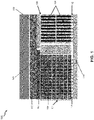
- FIG. 1 is a schematic diagram illustrating an example memory system 100 including a hybrid copper-bonded (HCB) bridge-connected memory stack 104, according to various aspects of the subject technology.
- the memory system 100 includes the HCB bridge-connected memory stack 104 (hereinafter, memory stack 100), a logic die 102 (e.g., including data-processing circuitry), a memory stack 104 (e.g., DRAM stack), an interposer 110, a buffer die 120, a silicon carrier 130, a heat sink 132, and a passive bridge die 140.
- the memory stack 104 includes a number of memory dies that are interconnected via copper bonding 108.
- the memory stack 104 is connected to the interposer 110 via conductive microbumps 112.
- the logic die 102 is coupled to the interposed 110 via copper bonding 108, through-silicon vias (TSVs) 124 and the conductive microbumps 112.
- the passive bridge die 140 is copper bonded to the logic die 102 and the buffer die 120 and provides interconnections between the logic die 102 and the memory stack 104.
- the implementation of the passive bridge die 140 as a medium to facilitate coupling the logic die 102 and the buffer die 120 memory stack 104 through copper bonding 108 is an important feature of the subject technology that allows the data signals to pass through copper bonding rather than TSVs and microbumps. This can increase the interconnection bandwidth between the logic die 102 and the memory stack 104. It should be noted that the structural features shown in FIG. 1 are not drawn to the scale.
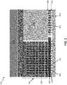
- FIG. 2 is a schematic diagram illustrating an example of a memory system 200 including an HBM stack 204 with a bottom overlapping buffer-die connection, according to various aspects of the subject technology.
- the memory system 200 includes the HBM stack 204 (e.g., DRAM stack), a logic die 202 (e.g., including data-processing circuitry), an interposer 210, a buffer die 220, a silicon carrier 230 and a heat sink 232.
- the HBM stack 204 includes a number of memory dies that are interconnected via copper bonding 208.
- the HBM stack 204 is connected to the interposer 210 via conductive microbumps 212.
- the logic die 202 is coupled to the interposer 210 via copper bonding 208, TSVs 224 passing through a support die 206, and the conductive microbumps 212.
- the buffer die 220 is extended toward the support dies die 206 and is connected to the logic die 202 via copper bonding 208.
- the buffer die 220 facilitates coupling the HBM stack 204 to the logic die 202 via copper bonding 208.
- the implementation of extension of the buffer die 220 as a medium to provide coupling between the logic die 202 and HBM stack 204 through copper bonding 208 is a significant feature of the present disclosure that allows the data signals to pass through copper bonding rather than TSVs and microbumps, which increases interconnection bandwidth between the logic die 202 and the HBM stack 204.
- the maximum data capacity is increased by the use of copper bonding within the layers of the stack, enabling a larger maximum number of layers through improved thermal conductance, mechanical integrity and electrical characteristics.
- the copper-bonded interconnection, through the bridge die in this case may not increase the capacity, but it does allow the system to take full advantage of the increased capacity, which otherwise would be bottle-necked by the narrower conventional interface between the memory and the logic die.
- the buffer die 220 is on the bottom of the HBM stack 204 with buffer extended to overlap the logic die 202 (processor).
- the support die 206 depth on the logic die 202 is limited to exactly one level. It should be noted that the structural features shown in FIG. 2 are not drawn to the scale.
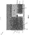
- FIG. 3 is a schematic diagram illustrating an example of a memory system 300 including an HBM stack 304 with a middle overlapping buffer-die connection, according to various aspects of the subject technology.
- the memory system 300 includes the HBM stack 304 (e.g., DRAM stack), a logic die 302 (e.g., including data-processing circuitry), an interposer 310, a buffer die 320, a silicon carrier 330 and a heat sink 332.
- the HBM stack 304 includes a number of memory dies that are interconnected via copper bonding 308.
- the HBM stack 304 is connected to the interposer 310 via conductive microbumps 312.
- the logic die 302 is coupled to the interposer 210 via copper bonding 308, TSVs 324 passing through support dies 306, and conductive microbumps 312.
- the buffer die 320 is disposed in the middle of the HBM stack 304 and is extended toward the support dies 306 and is connected to the logic die 302 via copper bonding 308.
- the middle buffer die 320 facilitates coupling the HBM stack 304 to the logic die 302 via copper bonding 308.
- the extension of the middle buffer die 320 as a medium to provide coupling between the logic die 302 and HBM stack 304 through copper bonding 308 is an important feature of the present disclosure and allows the data signals to pass through copper bonding rather than TSVs and microbumps, which increases the interconnection bandwidth between the logic die 302 and the HBM stack 304.
- the buffer die 320 is in the middle of the HBM stack 304 with the buffer die 320 extended to overlap the logic die 302 (processor).
- the support die 306 depth on logic die 302 is greater or equal to two levels. It should be noted that the structural features shown in FIG. 3 are not drawn to the scale.
- FIGs. 4A and 4B are diagrams illustrating an example of process flows 400A and 400B for fabricating an HBM dynamic DRAM stack connected by a passive HCB bridge, according to various aspects of the subject technology.
- the process flow 400A only shows major steps and skips descriptions of process flow for individual layers, which are well known.
- a structure 415 including a logic die 410 (e.g., including data-processing circuitry), a buffer die 420, with each of 410 and 420 including a copper bonding 408 and active layer 418 (including active elements such as transistors) are attached with face-down (i.e., with active surface 418 and copper bonding layer 408 oriented downward) on a temporary carrier 425, using temporary adhesive layer 409.
- a logic die 410 e.g., including data-processing circuitry
- a buffer die 420 with each of 410 and 420 including a copper bonding 408 and active layer 418 (including active elements such as transistors) are attached with face-down (i.
- process step 402 fillers 417 (e.g., dielectric material) are deposited and the structure 415 (including the buffer die 420 and logic die 410 are) is thinned to a desired thickness.
- process step 403 a silicon carrier layer 430 is permanently bonded to the in-process product of the process step 402, and the result is flipped so that the temporary carrier 425 can be removed in the next process step 404. It should be noted that what is described above with respect to processing a single die in practice applies ton entire wafer full of such dies that are processed simultaneously. Also, although the drawings only show one memory stack attached to the logic die, in actual use several memory stacks would be connected to each logic die, and various logic die might also themselves be interconnected to one another by copper-bonded bridge during the formation of the overall system.
- the process flow 400B of FIG. 4B is the continuation of the process flow 400A and includes process steps 405, 406 and 407.
- process step 405 the structure 435 including a HCB memory stack 424, a support die 426, a passive bridge 442 and corresponding active layers and copper bonding layers are prepared and face-to-face and die-to-wafer aligned with the in-process product of step 404 (e.g., reconstituted wafer)
- the memory stack 424, the passive bridge 442 and the support die 426 are copper bonded to the in-process product of step 404.
- the back surfaces of the attached die 424, 432, and 426 are machined (e.g., using chemical-mechanical polishing) to a desired thickness to reveal the TSVs.
- the structure is then completed by addition of solder microbumps or pillars and attaching of the interposer and heat sink (steps not shown) to produce the memory system 100 of FIG. 1 .
- FIGs. 5A , 5B and 5C are diagrams illustrating an example of process flows 500A, 500B and 500C for fabricating an HCB DRAM stack with overlapping buffer at the bottom of the stack, according to various aspects of the subject technology.
- the process flow 500A only shows major steps and skips descriptions of process flow for individual layers, which are well known.
- a logic die e.g., including a processor
- a memory stack die 524 e.g., the HCB DRAM stack
- fillers 517 e.g., dielectric material
- a silicon carrier wafer 530 is permanently bonded to the in-process product of the process step 502 and the result is flipped so that the temporary carrier 525 can be removed in a next process step 504 of FIG. 5B .
- the process flow 500B of FIG. 5B is the continuation of the process flow 500A and includes process steps 504, 505 and 506 and 507.
- the temporary carrier 525 is removed so that the logic die 510 and the memory stack die 524 and corresponding copper bonding layers are exposed.
- a buffer die 520, a support die 516 and corresponding active layers and copper bonding layers are prepared and face-to-face and die-to-wafer aligned with the in-process product of step 504.
- the buffer die 520 and support die 516 of process step 505 is copper bonded to the already aligned in-process product of step 504.
- FIG. 5C is the continuation of the process flow 500B and includes process step 507.
- the buffer die 520 and support die 516 which are bonded to the in-process product of step 504, is machined (e.g., by chemical-mechanical polishing) to a desired thickness to produce part of the memory system 300 of FIG. 3 (e.g., the logic die 302, a top portion of memory stack 304, the buffer dies 320, the support die 308 and the silicon carrier 330).
- FIGs. 6A , 6B , 6C and 6D are diagrams illustrating an example of process flows 600A, 600B, 600C and 600D for fabricating an HCB DRAM stack with overlapping buffer in the middle of the stack, according to various aspects of the subject technology.
- the description herein is of placement of the overlapping copper-bonded buffer exactly in the middle of the stack ("half-stacks" on either side), for minimizing the worst-case path latency, in some implementations, the buffer could be anywhere within the stack.
- the process flow 600A only shows major steps and skips descriptions of process flow for individual layers, which are well known.
- a logic die e.g., including a processor
- a half memory stack 624 e.g., the HCB DRAM stack
- fillers 617 are deposited to fill gaps as shown in FIG. 6A .
- a silicon carrier wafer 630 is permanently bonded to the in-process product of the process step 602 and the result is flipped so that the temporary carrier 625 can be removed in a next process step 604 of FIG. 6B .
- the process flow 600B of FIG. 6B is the continuation of the process flow 600A and includes process steps 604, 605 and 606.
- the temporary carrier 625 is removed so that the logic die 610 and the half memory stack die 624 and corresponding copper bonding layers are exposed.
- a buffer die 620, a support die 616 and corresponding active layers and copper bonding layers are prepared and face-to-face and die-to-wafer aligned with the in-process product of step 604.
- the buffer die 620 and support die 616 of process step 605 are copper bonded to the already aligned in-process product of step 604.
- FIG. 6C is the continuation of the process flow 600B and includes process steps 607 and 608.
- the buffer die 620 and support die 616 which is are bonded to the in-process product of step 604, is are machined to a desired thickness, exposing the TSVs.
- the process step 607b shows preparation of the product of process step 607a for subsequent copper bonding by addition of patterned copper bonding layers 615 over the revealed TSVs.
- a half memory stack 626 and a second support die 618 and corresponding active layers and copper bonding are prepared and face-to-face and die-to-wafer aligned with the in-process product of step 607.
- FIG. 6D is the continuation of the process flow 600C and includes process steps 609 and 610.
- process steps 609 the half memory stack 626 and a second support die 618 are permanently bonded to the in-process product of step 607b.
- process steps 610 the half memory stack 626 and the second support die 618, which are bonded to the in-process product of step 607b, are machined to a desired thickness, exposing the TSVs.
- a half memory stack 626 and a second support die 618 and corresponding active layers and copper bonding are prepared and face-to-face and die-to-wafer aligned with the in-process product of step 607 to produce part of the memory system 200 of FIG. 2 (e.g., the logic die 202, memory stack 204, the buffer dies 220, the support die 208 and the silicon carrier 230).
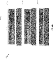
- FIG. 7 is diagram illustrating a comparison of HCB-connected DRAM stack configuration 710, 720 and 730, according to various aspects of the subject technology.
- the HCB-connected DRAM stack configuration 710, 720 and 730 are respectively the products of process flows of FIG. 4 ( 4A and 4B ), FIG. 5 ( 5A , 5B and 5C ) and FIG. 6 ( 6A , 6B , 6C and 6D ) and are completed by addition of a copper redistribution layer with associated dielectrics and solder microbumps for connection to an interposer or other packages.
- primary heat removal is through the top surface, which is the back surface of the silicon carrier.
- the silicon carrier might include embedded microfluidic cooling.
- Power and ground connections are provided for the DRAM stack (and to the logic die) through the microbump connections to the interposer or other packages (not shown) connected to the revealed TSV arrays at the bottom of surface as oriented in configurations of FIG. 7 .
- the configuration 710 and 730 power and ground for the buffer die is fed through the DRAM stack
- the TSV arrays in the DRAM stack carry only power for the DRAM layers (as in a conventional HBM).
- the external connections to the logic die need to be brought down to the same interposer/package plane used by the bottom TSV connections on the DRAM stack. As shown in the diagrams of FIG. 7 , this could be done through one or more layers of support die stacked with the logic die, or it might be accomplished using through dielectric vias (not shown). Additional methods for making these external connections to the dummy die might include substitution of passive glass die with through-glass vias for the support die presently shown, or the use of three-dimensional spring structures formed on and released from an interposer surface.
- the three configurations 710, 720 and 730 provide different depths available for the stacking of support die, with the bridge-die configurations 710 providing the most depth, the buffer-on-bottom configuration 720 providing the least, and the buffer-in-middle configuration 730 the providing a medium depth.
- the buffer-in-middle configuration 730 has a potential benefit in that the maximum vertical distance from any DRAM layer to the buffer is cut in half compared to the other configurations, possibly improving efficiency or reducing latency.
- FIG. 8 is a schematic diagram illustrating an example of a conventional memory stack 800.
- the conventional memory system 800 includes the HBM stack 804 (e.g., DRAM stack), a logic die 802 (e.g., including a data-processing circuitry), an interposer 810, a buffer die 820 and a heat sink 832.
- the HBM stack 804 includes a number of memory dies that are interconnected via solder microbump interconnections 808.
- the HBM stack 804 is connected to buffer die 820 via solder microbumps 808, the buffer die 820 is connected face down to interposer 810 through solder bumps 812, power-delivery network (PDN) for logic die 802 is achieved through TSV and solder bumps and communication between the logic die 802 and the HBM stack 804 is provided through solder bumps and interposer.
- PDN power-delivery network
- the buffer die connected with back surface to silicon carrier, PDN for both memory die and buffer die is through TSV and copper-to-copper bonds
- communication to processor is provided through copper-bonded bridge, as described above with respect to FIG. 1 .
- the subject technology has a number of applications, for example, the application in high-performance logic systems, such as processing units or networking equipment typically installed in data centers. Systems requiring the memory capacity of such memory stacks typically consume too much power and produce too much heat for mobile applications.
- any specific order or hierarchy of blocks in the processes disclosed is an illustration of example approaches. Based upon design preferences, it is understood that the specific order or hierarchy of blocks in the processes may be rearranged, or that all illustrated blocks should be performed. Any of the blocks may be simultaneously performed. In one or more implementations, multitasking and parallel processing may be advantageous. Moreover, the separation of various system components in the embodiments described above should not be understood as requiring such separation in all embodiments, and it should be understood that the described program components and systems could generally be integrated together in a single software product or packaged into multiple software products.
- base station As used in this specification and any claims of this application, the terms “base station,” “receiver,” “computer,” “server,” “processor,” and “memory” all refer to electronic or other technological devices. These terms exclude people or groups of people.
- display or “displaying” means displaying on an electronic device.
- the phrase "at least one of' preceding a series of items, with the term “and” or “or” to separate any of the items, modifies the list as a whole, rather than each member of the list (i.e., each item).
- phrases “at least one of A, B, and C” and “at least one of A, B, or C” each refer to only A, only B, or only C; any combination of A, B, and C; and/or at least one of each of A, B, and C.
- a processor configured to monitor and control an operation or a component may also mean the processor being programmed to monitor and control the operation or the processor being operable to monitor and control the operation.
- a processor configured to execute code can be construed as a processor programmed to execute code or operable to execute code.
- phrases such as “an aspect,” “the aspect,” “another aspect,” “some aspects,” “one or more aspects,” “an implementation,” “the implementation,” “another implementation,” “some implementations,” “one or more implementations,” “an embodiment,” “the embodiment,” “another embodiment,” “some embodiments,” “one or more embodiments,” “a configuration,” “the configuration,” “another configuration,” “some configurations,” “one or more configurations,” “the subject technology,” “the disclosure,” “the present disclosure,” and other variations thereof and alike are for convenience and do not imply that a disclosure relating to such phrase(s) is essential to the subject technology or that such disclosure applies to all configurations of the subject technology. A disclosure relating to such phrase(s) may apply to all configurations, or one or more configurations. A disclosure relating to such phrase(s) may provide one or more examples.
- a phrase such as “an aspect” or “some aspects” may refer to one or more aspects and vice versa, and this applies similarly to other foregoing phrases.
Landscapes
- Semiconductor Memories (AREA)
- Engineering & Computer Science (AREA)
- Manufacturing & Machinery (AREA)
Abstract
Description
- The present description relates generally to integrated circuits and, in particular, to copper-bonded memory stacks with copper-bonded interconnection memory systems.
- High-bandwidth memory (HBM) is widely used to provide a large-capacity memory with high-bandwidth interconnection to a processing logic die in an integrated module for high-performance computing, artificial intelligence, machine learning and other applications. Conventional HBM is implemented with several layers of dynamic random-access memory (DRAM) die stacked on a buffer die using solder microbump interconnections. Direct copper bonding (hybrid copper bonding or copper-fusion bonding, hereafter referred to as "copper bonding") can provide much denser interconnection pitch compared to solder microbumps, while also reducing the thermal resistance and parasitic electrical impedance between the bonded die.
- Replacing the solder microbumps with copper bonding has the potential to significantly increase the practical stacking limit in HBM stacks. For example, present solder-bonded maximum stack height is perhaps 12 layers. However, with copper bonding 24 or 32 layers might be stacked with thinner silicon per layer, lower thermal resistance, and higher bonding yields. As copper bonding is used to increase the maximum capacity in HBM stacks, a memory structure is needed to use copper bonding to also increase the interconnection bandwidth between HBM stacks and logic die.
- Certain features of the subject technology are set forth in the appended claims. However, for purposes of explanation, several embodiments of the subject technology are set forth in the following figures.
-
FIG. 1 is a schematic diagram illustrating an example of a memory system including a hybrid copper-bonded (HCB) bridge-connected memory stack, according to various aspects of the subject technology. -
FIG. 2 is a schematic diagram illustrating an example of a memory system including a high-bandwidth memory (HBM) stack with a bottom overlapping buffer-die connection, according to various aspects of the subject technology. -
FIG. 3 is a schematic diagram illustrating an example of a memory system including an HBM stack with a middle overlapping buffer-die connection, according to various aspects of the subject technology. -
FIGs. 4A and4B are diagrams illustrating an example of a process flow for fabricating an HBM dynamic random-access memory (DRAM) stack connected by a passive hybrid copper-bonded (HCB) bridge, according to various aspects of the subject technology. -
FIGs. 5A ,5B and5C are diagrams illustrating an example of a process flow for fabricating an HCB DRAM stack with overlapping buffer at the bottom of the stack, according to various aspects of the subject technology. -
FIGs. 6A ,6B ,6C , and6D are diagrams illustrating an example of a process flow for fabricating an HCB DRAM stack with overlapping buffer in the middle of the stack, according to various aspects of the subject technology. -
FIG. 7 is a diagram illustrating a comparison of HCB-connected DRAM stack configuration, according to various aspects of the subject technology. -
FIG. 8 is a schematic diagram illustrating an example of a conventional memory stack. - The detailed description set forth below is intended as a description of various configurations of the subject technology and is not intended to represent the only configurations in which the subject technology may be practiced. The appended drawings are incorporated herein and constitute part of the detailed description, which includes specific details for providing a thorough understanding of the subject technology. However, the subject technology is not limited to the specific details set forth herein and may be practiced without one or more of the specific details. In some instances, structures and components are shown in a block-diagram form in order to avoid obscuring the concepts of the subject technology.
- The subject technology is directed to memory systems and systems for copper-bonded memory stacks with copper-bonded interconnection memory systems. The disclosed invention defines three different physical configurations for replacing the solder microbump and interposer and/or package connection from the HBM to the logic die with copper-bonded connections, along with process sequences for assembly of the proposed copper-bonded HBMs with copper-bonded connections to logic die. The copper-bonded interconnection memory systems of the subject technology increase the interconnection bandwidth between high-bandwidth-memory (HBM) stacks and logic die. Conventional HBM achieves high-bandwidth interconnection relative to other conventional memories through a wider connection to the logic die, i.e., a connection with a larger number of data wires. In the case of traditional HBM memory, the width of the interface is 1,024 data wires (compared to 64 data wires in other conventional memories, for example). Memory stacks with copper-bonded interconnect can significantly increase the number of data wires, and thus the interconnection bandwidth, compared to conventional solder-bonded HBMs. The increased data-wire capacity comes from decreased copper-bonded connection pitch compared to solder microbump pitch.
- A conventional HBM stack might use a 55 µm solder microbump pitch, while a copper-bonded memory stack might have a 9 µm connection pitch (or less), for a connection density multiplier of 552 / 92 that is greater than 37 times. The increased interconnection density with copper bonding also allows much shorter link distances as the connection array area decreases drastically. In conventional HBMs, link wire lengths are typically several millimeters, while copper-bonded link lengths might be half a millimeter or less. Reduced link lengths and reduced parasitic capacitance, resistance, and inductance of copper-bonded connections also allow higher energy efficiency compared to a conventional solder-bonded HBM.
- The increased interconnection bandwidth provided by copper-bonded interconnect is important to realizing the full potential benefit of copper-bonded dynamic random-access memory (DRAM) stacks. Copper-bonded stacks can potentially significantly increase memory-stack capacity by increasing the practical limits on the number of layers in the stack, due to improved thermal conductivity, improved bonding yield, and increased planarity and mechanical integrity supporting thinner individual DRAM silicon layers. But the value of the increasing total capacity of the copper-bonded DRAM stack may not be fully realized in system functionality if the interconnection bandwidth does not also increase.
-
FIG. 1 is a schematic diagram illustrating anexample memory system 100 including a hybrid copper-bonded (HCB) bridge-connectedmemory stack 104, according to various aspects of the subject technology. Thememory system 100 includes the HCB bridge-connected memory stack 104 (hereinafter, memory stack 100), a logic die 102 (e.g., including data-processing circuitry), a memory stack 104 (e.g., DRAM stack), aninterposer 110, a buffer die 120, asilicon carrier 130, aheat sink 132, and apassive bridge die 140. Thememory stack 104 includes a number of memory dies that are interconnected viacopper bonding 108. Thememory stack 104 is connected to theinterposer 110 viaconductive microbumps 112. The logic die 102 is coupled to the interposed 110 viacopper bonding 108, through-silicon vias (TSVs) 124 and theconductive microbumps 112. The passive bridge die 140 is copper bonded to the logic die 102 and the buffer die 120 and provides interconnections between the logic die 102 and thememory stack 104. The implementation of the passive bridge die 140 as a medium to facilitate coupling the logic die 102 and the buffer die 120memory stack 104 throughcopper bonding 108 is an important feature of the subject technology that allows the data signals to pass through copper bonding rather than TSVs and microbumps. This can increase the interconnection bandwidth between thelogic die 102 and thememory stack 104. It should be noted that the structural features shown inFIG. 1 are not drawn to the scale. -
FIG. 2 is a schematic diagram illustrating an example of amemory system 200 including anHBM stack 204 with a bottom overlapping buffer-die connection, according to various aspects of the subject technology. Thememory system 200 includes the HBM stack 204 (e.g., DRAM stack), a logic die 202 (e.g., including data-processing circuitry), aninterposer 210, a buffer die 220, asilicon carrier 230 and aheat sink 232. TheHBM stack 204 includes a number of memory dies that are interconnected viacopper bonding 208. TheHBM stack 204 is connected to theinterposer 210 viaconductive microbumps 212. The logic die 202 is coupled to theinterposer 210 viacopper bonding 208,TSVs 224 passing through a support die 206, and theconductive microbumps 212. The buffer die 220 is extended toward the support dies die 206 and is connected to the logic die 202 viacopper bonding 208. The buffer die 220 facilitates coupling theHBM stack 204 to the logic die 202 viacopper bonding 208. The implementation of extension of the buffer die 220 as a medium to provide coupling between thelogic die 202 andHBM stack 204 throughcopper bonding 208 is a significant feature of the present disclosure that allows the data signals to pass through copper bonding rather than TSVs and microbumps, which increases interconnection bandwidth between thelogic die 202 and theHBM stack 204. The maximum data capacity is increased by the use of copper bonding within the layers of the stack, enabling a larger maximum number of layers through improved thermal conductance, mechanical integrity and electrical characteristics. The copper-bonded interconnection, through the bridge die in this case, may not increase the capacity, but it does allow the system to take full advantage of the increased capacity, which otherwise would be bottle-necked by the narrower conventional interface between the memory and the logic die. As described above, in thememory system 200, thebuffer die 220 is on the bottom of theHBM stack 204 with buffer extended to overlap the logic die 202 (processor). The support die 206 depth on the logic die 202 is limited to exactly one level. It should be noted that the structural features shown inFIG. 2 are not drawn to the scale. -
FIG. 3 is a schematic diagram illustrating an example of amemory system 300 including anHBM stack 304 with a middle overlapping buffer-die connection, according to various aspects of the subject technology. Thememory system 300 includes the HBM stack 304 (e.g., DRAM stack), a logic die 302 (e.g., including data-processing circuitry), aninterposer 310, abuffer die 320, asilicon carrier 330 and aheat sink 332. TheHBM stack 304 includes a number of memory dies that are interconnected viacopper bonding 308. TheHBM stack 304 is connected to theinterposer 310 viaconductive microbumps 312. The logic die 302 is coupled to theinterposer 210 viacopper bonding 308,TSVs 324 passing through support dies 306, andconductive microbumps 312. The buffer die 320 is disposed in the middle of theHBM stack 304 and is extended toward the support dies 306 and is connected to the logic die 302 viacopper bonding 308. The middle buffer die 320 facilitates coupling theHBM stack 304 to the logic die 302 viacopper bonding 308. Therefore, the extension of the middle buffer die 320 as a medium to provide coupling between the logic die 302 andHBM stack 304 throughcopper bonding 308 is an important feature of the present disclosure and allows the data signals to pass through copper bonding rather than TSVs and microbumps, which increases the interconnection bandwidth between the logic die 302 and theHBM stack 304. In thememory system 300, the buffer die 320 is in the middle of theHBM stack 304 with the buffer die 320 extended to overlap the logic die 302 (processor). The support die 306 depth on logic die 302 is greater or equal to two levels. It should be noted that the structural features shown inFIG. 3 are not drawn to the scale. -
FIGs. 4A and4B are diagrams illustrating an example of process flows 400A and 400B for fabricating an HBM dynamic DRAM stack connected by a passive HCB bridge, according to various aspects of the subject technology. The process flow 400A only shows major steps and skips descriptions of process flow for individual layers, which are well known. Inprocess step 401, astructure 415 including a logic die 410 (e.g., including data-processing circuitry), abuffer die 420, with each of 410 and 420 including acopper bonding 408 and active layer 418 (including active elements such as transistors) are attached with face-down (i.e., withactive surface 418 andcopper bonding layer 408 oriented downward) on atemporary carrier 425, using temporaryadhesive layer 409. These dies have been fabricated by normal wafer fabrication processes through the standard interconnect stack completion, followed by addition of the copper bonding layers 408, and singulation, prior to attach to the temporary carrier in the first drawing 401). Inprocess step 402, fillers 417 (e.g., dielectric material) are deposited and the structure 415 (including the buffer die 420 and logic die 410 are) is thinned to a desired thickness. Inprocess step 403, asilicon carrier layer 430 is permanently bonded to the in-process product of theprocess step 402, and the result is flipped so that thetemporary carrier 425 can be removed in thenext process step 404. It should be noted that what is described above with respect to processing a single die in practice applies ton entire wafer full of such dies that are processed simultaneously. Also, although the drawings only show one memory stack attached to the logic die, in actual use several memory stacks would be connected to each logic die, and various logic die might also themselves be interconnected to one another by copper-bonded bridge during the formation of the overall system. - The
process flow 400B ofFIG. 4B is the continuation of theprocess flow 400A and includes process steps 405, 406 and 407. Inprocess step 405, thestructure 435 including aHCB memory stack 424, a support die 426, apassive bridge 442 and corresponding active layers and copper bonding layers are prepared and face-to-face and die-to-wafer aligned with the in-process product of step 404 (e.g., reconstituted wafer)Inprocess step 406, thememory stack 424, thepassive bridge 442 and the support die 426 are copper bonded to the in-process product ofstep 404. Inprocess step 407, the back surfaces of the attacheddie step 404, are machined (e.g., using chemical-mechanical polishing) to a desired thickness to reveal the TSVs. The structure is then completed by addition of solder microbumps or pillars and attaching of the interposer and heat sink (steps not shown) to produce thememory system 100 ofFIG. 1 . -
FIGs. 5A ,5B and5C are diagrams illustrating an example of process flows 500A, 500B and 500C for fabricating an HCB DRAM stack with overlapping buffer at the bottom of the stack, according to various aspects of the subject technology. The process flow 500A only shows major steps and skips descriptions of process flow for individual layers, which are well known. Inprocess step 501, a logic die (e.g., including a processor) 510 and a memory stack die 524 (e.g., the HCB DRAM stack) are mounted on atemporary carrier 525 using a temporaryadhesive layer 513. Inprocess step 502, fillers 517 (e.g., dielectric material) are deposited to fill gaps as shown inFIG. 5A . Inprocess step 503, asilicon carrier wafer 530 is permanently bonded to the in-process product of theprocess step 502 and the result is flipped so that thetemporary carrier 525 can be removed in anext process step 504 ofFIG. 5B . - The
process flow 500B ofFIG. 5B is the continuation of theprocess flow 500A and includes process steps 504, 505 and 506 and 507. Inprocess step 504, thetemporary carrier 525 is removed so that the logic die 510 and the memory stack die 524 and corresponding copper bonding layers are exposed. Inprocess step 505, abuffer die 520, a support die 516 and corresponding active layers and copper bonding layers are prepared and face-to-face and die-to-wafer aligned with the in-process product ofstep 504. Inprocess step 506, the buffer die 520 and support die 516 ofprocess step 505 is copper bonded to the already aligned in-process product ofstep 504. -
FIG. 5C is the continuation of theprocess flow 500B and includesprocess step 507. In theprocess step 507, the buffer die 520 and support die 516, which are bonded to the in-process product ofstep 504, is machined (e.g., by chemical-mechanical polishing) to a desired thickness to produce part of thememory system 300 ofFIG. 3 (e.g., the logic die 302, a top portion ofmemory stack 304, the buffer dies 320, the support die 308 and the silicon carrier 330). -
FIGs. 6A ,6B ,6C and6D are diagrams illustrating an example of process flows 600A, 600B, 600C and 600D for fabricating an HCB DRAM stack with overlapping buffer in the middle of the stack, according to various aspects of the subject technology. Although the description herein is of placement of the overlapping copper-bonded buffer exactly in the middle of the stack ("half-stacks" on either side), for minimizing the worst-case path latency, in some implementations, the buffer could be anywhere within the stack. The process flow 600A only shows major steps and skips descriptions of process flow for individual layers, which are well known. Inprocess step 601, a logic die (e.g., including a processor) 610 and a half memory stack 624 (e.g., the HCB DRAM stack) are bonded to atemporary carrier 625 using a temporaryadhesive layer 613. Inprocess step 602, fillers 617 (e.g., dielectric material) are deposited to fill gaps as shown inFIG. 6A . Inprocess step 603, asilicon carrier wafer 630 is permanently bonded to the in-process product of theprocess step 602 and the result is flipped so that thetemporary carrier 625 can be removed in anext process step 604 ofFIG. 6B . - The
process flow 600B ofFIG. 6B is the continuation of theprocess flow 600A and includes process steps 604, 605 and 606. Inprocess step 604, thetemporary carrier 625 is removed so that the logic die 610 and the half memory stack die 624 and corresponding copper bonding layers are exposed. Inprocess step 605, abuffer die 620, a support die 616 and corresponding active layers and copper bonding layers are prepared and face-to-face and die-to-wafer aligned with the in-process product ofstep 604. Inprocess step 606, the buffer die 620 and support die 616 ofprocess step 605 are copper bonded to the already aligned in-process product ofstep 604. -
FIG. 6C is the continuation of theprocess flow 600B and includes process steps 607 and 608. In theprocess step 607a, the buffer die 620 and support die 616, which is are bonded to the in-process product ofstep 604, is are machined to a desired thickness, exposing the TSVs. Theprocess step 607b shows preparation of the product ofprocess step 607a for subsequent copper bonding by addition of patterned copper bonding layers 615 over the revealed TSVs. In theprocess step 608, ahalf memory stack 626 and a second support die 618 and corresponding active layers and copper bonding are prepared and face-to-face and die-to-wafer aligned with the in-process product of step 607. -
FIG. 6D is the continuation of theprocess flow 600C and includes process steps 609 and 610. In process steps 609, thehalf memory stack 626 and a second support die 618 are permanently bonded to the in-process product ofstep 607b. In process steps 610, thehalf memory stack 626 and the second support die 618, which are bonded to the in-process product ofstep 607b, are machined to a desired thickness, exposing the TSVs. In theprocess step 608, ahalf memory stack 626 and a second support die 618 and corresponding active layers and copper bonding are prepared and face-to-face and die-to-wafer aligned with the in-process product of step 607 to produce part of thememory system 200 ofFIG. 2 (e.g., the logic die 202,memory stack 204, the buffer dies 220, the support die 208 and the silicon carrier 230). -
FIG. 7 is diagram illustrating a comparison of HCB-connectedDRAM stack configuration DRAM stack configuration FIG. 4 (4A and4B ),FIG. 5 (5A ,5B and5C ) andFIG. 6 (6A ,6B ,6C and6D ) and are completed by addition of a copper redistribution layer with associated dielectrics and solder microbumps for connection to an interposer or other packages. In the orientation shown in these configurations, primary heat removal is through the top surface, which is the back surface of the silicon carrier. Note that the silicon carrier might include embedded microfluidic cooling. - Power and ground connections are provided for the DRAM stack (and to the logic die) through the microbump connections to the interposer or other packages (not shown) connected to the revealed TSV arrays at the bottom of surface as oriented in configurations of
FIG. 7 . Note that in theconfiguration configuration 720, the TSV arrays in the DRAM stack carry only power for the DRAM layers (as in a conventional HBM). - The external connections to the logic die need to be brought down to the same interposer/package plane used by the bottom TSV connections on the DRAM stack. As shown in the diagrams of
FIG. 7 , this could be done through one or more layers of support die stacked with the logic die, or it might be accomplished using through dielectric vias (not shown). Additional methods for making these external connections to the dummy die might include substitution of passive glass die with through-glass vias for the support die presently shown, or the use of three-dimensional spring structures formed on and released from an interposer surface. The threeconfigurations configurations 710 providing the most depth, the buffer-on-bottom configuration 720 providing the least, and the buffer-in-middle configuration 730 the providing a medium depth. The buffer-in-middle configuration 730 has a potential benefit in that the maximum vertical distance from any DRAM layer to the buffer is cut in half compared to the other configurations, possibly improving efficiency or reducing latency. -
FIG. 8 is a schematic diagram illustrating an example of aconventional memory stack 800. Theconventional memory system 800 includes the HBM stack 804 (e.g., DRAM stack), a logic die 802 (e.g., including a data-processing circuitry), aninterposer 810, a buffer die 820 and aheat sink 832. TheHBM stack 804 includes a number of memory dies that are interconnected viasolder microbump interconnections 808. TheHBM stack 804 is connected to buffer die 820 viasolder microbumps 808, the buffer die 820 is connected face down tointerposer 810 throughsolder bumps 812, power-delivery network (PDN) for logic die 802 is achieved through TSV and solder bumps and communication between the logic die 802 and theHBM stack 804 is provided through solder bumps and interposer. In the implementation of the subject technology (e.g., 710 ofFIG. 7 ) the buffer die connected with back surface to silicon carrier, PDN for both memory die and buffer die is through TSV and copper-to-copper bonds, and communication to processor is provided through copper-bonded bridge, as described above with respect toFIG. 1 . - The subject technology has a number of applications, for example, the application in high-performance logic systems, such as processing units or networking equipment typically installed in data centers. Systems requiring the memory capacity of such memory stacks typically consume too much power and produce too much heat for mobile applications.
- Those of skill in the art would appreciate that the various illustrative blocks, modules, elements, components, memory systems, and algorithms described herein may be implemented as electronic hardware, computer software, or combinations of both. To illustrate this interchangeability of hardware and software, various illustrative blocks, modules, elements, components, memory systems, and algorithms have been described above generally in terms of their functionality. Whether such functionality is implemented as hardware or software depends upon the particular application and design constraints imposed on the overall system. Skilled artisans may implement the described functionality in varying ways for each particular application. Various components and blocks may be arranged differently (e.g., arranged in a different order, or partitioned in a different way) all without departing from the scope of the subject technology.
- It is understood that any specific order or hierarchy of blocks in the processes disclosed is an illustration of example approaches. Based upon design preferences, it is understood that the specific order or hierarchy of blocks in the processes may be rearranged, or that all illustrated blocks should be performed. Any of the blocks may be simultaneously performed. In one or more implementations, multitasking and parallel processing may be advantageous. Moreover, the separation of various system components in the embodiments described above should not be understood as requiring such separation in all embodiments, and it should be understood that the described program components and systems could generally be integrated together in a single software product or packaged into multiple software products.
- As used in this specification and any claims of this application, the terms "base station," "receiver," "computer," "server," "processor," and "memory" all refer to electronic or other technological devices. These terms exclude people or groups of people. For the purposes of the specification, the term "display" or "displaying" means displaying on an electronic device.
- As used herein, the phrase "at least one of' preceding a series of items, with the term "and" or "or" to separate any of the items, modifies the list as a whole, rather than each member of the list (i.e., each item). The phrase "at least one of' does not require selection of at least one of each item listed; rather, the phrase allows a meaning that includes at least one of any one of the items, and/or at least one of any combination of the items, and/or at least one of each of the items. By way of example, the phrases "at least one of A, B, and C" and "at least one of A, B, or C" each refer to only A, only B, or only C; any combination of A, B, and C; and/or at least one of each of A, B, and C.
- The predicate words "configured to," "operable to," and "programmed to" do not imply any particular tangible or intangible modification of a subject but rather are intended to be used interchangeably. In one or more implementations, a processor configured to monitor and control an operation or a component may also mean the processor being programmed to monitor and control the operation or the processor being operable to monitor and control the operation. Likewise, a processor configured to execute code can be construed as a processor programmed to execute code or operable to execute code.
- Phrases such as "an aspect," "the aspect," "another aspect," "some aspects," "one or more aspects," "an implementation," "the implementation," "another implementation," "some implementations," "one or more implementations," "an embodiment," "the embodiment," "another embodiment," "some embodiments," "one or more embodiments," "a configuration," "the configuration," "another configuration," "some configurations," "one or more configurations," "the subject technology," "the disclosure," "the present disclosure," and other variations thereof and alike are for convenience and do not imply that a disclosure relating to such phrase(s) is essential to the subject technology or that such disclosure applies to all configurations of the subject technology. A disclosure relating to such phrase(s) may apply to all configurations, or one or more configurations. A disclosure relating to such phrase(s) may provide one or more examples. A phrase such as "an aspect" or "some aspects" may refer to one or more aspects and vice versa, and this applies similarly to other foregoing phrases.
- The word "exemplary" is used herein to mean "serving as an example, instance, or illustration." Any embodiment described herein as "exemplary" or as an "example" is not necessarily to be construed as preferred or advantageous over other embodiments. Furthermore, to the extent that the term "include," "have," or the like is used in the description or the claims, such term is intended to be inclusive in a manner similar to the term "comprise" as "comprise" is interpreted when employed as a transitional word in a claim.
- All structural and functional equivalents to the elements of the various aspects described throughout this disclosure that are known or later come to be known to those of ordinary skilled in the art are expressly incorporated herein by reference and are intended to be encompassed by the claims. Moreover, nothing disclosed herein is intended to be dedicated to the public, regardless of whether such disclosure is explicitly recited in the claims. No claim element is to be construed under the provisions of 35 U.S.C. § 112(f) unless the element is expressly recited using the phrase "means for" or, in the case of a memory system claim, the element is recited using the phrase "step for."
- The previous description is provided to enable any person skilled in the art to practice the various aspects described herein. Various modifications to these aspects would be readily apparent to those skilled in the art, and the generic principles defined herein may be applied to other aspects. Thus, the claims are not intended to be limited to the aspects shown herein, but are to be accorded the full scope consistent with the language claims, wherein reference to an element in the singular is not intended to mean "one and only one" unless specifically so stated, but rather "one or more." Unless specifically stated otherwise, the term "some" refers to one or more. Pronouns in the masculine (e.g., his) include the feminine and neuter gender (e.g., her and its) and vice versa. Headings and subheadings, if any, are used for convenience only and do not limit the subject disclosure.
Claims (15)
- A memory system comprising:a memory stack including a plurality of memory dies interconnected via copper bonding;a logic die coupled to the memory stack via a copper bonding;a buffer die extended to provide the copper bonding between the logic die and the memory stack; anda silicon carrier layer bonded to the memory stack and the logic die.
- The memory system of claim 1, wherein the buffer dies is located in a middle position of the memory stack.
- The memory system of claim 1 or 2, wherein the buffer die is located in a bottom position of the memory stack.
- The memory system of claim 3, further comprising a passive bridge die located between the memory stack and the logic die, wherein in particular the passive bridge die is conductively coupled to the logic die and the buffer die via copper bonding, and wherein the buffer dies is connected to the memory stack via copper bonding.
- The memory system of any of claims 1 to 4, comprising at least one of the following features:wherein the logic die includes one or data-processing circuitry;wherein the memory stack comprises hybrid-copper boded (HCB) memory including dynamic random-access memory (DRAM).
- The memory system of any of claims 1 to 5, further comprising an interposer layer conductively coupled to the logic die and the memory stack.
- The memory system of claim 6, wherein the interposer layer is coupled to the logic die via one or more support dies including through-silicon vias (TSVs) coupled to one another and to the logic die via copper bonding.
- The memory system of claim 7, further comprising a heatsink layer bonded to the silicon carrier layer.
- A method comprising:fabricating a memory stack by interconnecting a plurality of memory dies via copper bonding;coupling a logic die to the memory stack via copper bonding;disposing an extended buffer die to provide the copper bonding between the logic die and the memory stack; andbonding a silicon carrier layer to the memory stack and the logic die.
- The method of claim 9, further comprising disposing the extended buffer die in a bottom position of the memory stack.
- The method of claim 9 or 10, further comprising disposing the extended buffer die in a middle position of the memory stack.
- The method of claim 11, further comprising:disposing a passive bridge die between the memory stack and the logic die;conductively coupling the passive bridge die to the logic die and the extended buffer die via copper bonding; andconnecting the extended buffer dies to the memory stack via copper bonding.
- The method of any of claims 9 to 12, comprising at least one of the following features:further comprising conductively coupling an interposer layer to the logic die and the memory stack, in particular further comprising: coupling the interposer layer to the logic die via one ormore support dies including TSVs and coupling the one or more support dies to one another and to the logic die via copper bonding;further comprising bonding a heatsink layer to the silicon carrier layer;wherein fabricating the memory stack comprises fabricating a HCB memory including DRAM, and wherein coupling the logic die comprises coupling data-processing circuitry.
- A system comprising:memory; anda processor coupled to the memory,wherein:the memory comprises a memory stack including a plurality of memory dies interconnected via copper bonding;the processor is implemented on a logic die coupled to the memory stack via a copper bonding; andan extended buffer die is used to provide the copper bonding between the logic die and the memory stack.
- The system of claim 14, wherein:the extended buffer die is located in one of a middle position or a bottom position of the memory stack,an interposer layer is coupled to the logic die via one or more support dies including TSVs coupled to one another and to the logic die via copper bonding, andthe interposer layer is coupled to the memory stack through solder microbumps.
Applications Claiming Priority (1)
| Application Number | Priority Date | Filing Date | Title |
|---|---|---|---|
| US17/331,196 US11721685B2 (en) | 2021-05-26 | 2021-05-26 | Copper-bonded memory stacks with copper-bonded interconnection memory systems |
Publications (1)
| Publication Number | Publication Date |
|---|---|
| EP4095908A1 true EP4095908A1 (en) | 2022-11-30 |
Family
ID=81850648
Family Applications (1)
| Application Number | Title | Priority Date | Filing Date |
|---|---|---|---|
| EP22175023.5A Pending EP4095908A1 (en) | 2021-05-26 | 2022-05-24 | Copper-bonded memory dies in a memory stack which is copper-bonded to a logic die via a buffer die |
Country Status (3)
| Country | Link |
|---|---|
| US (3) | US11721685B2 (en) |
| EP (1) | EP4095908A1 (en) |
| CN (1) | CN115411038B (en) |
Families Citing this family (3)
| Publication number | Priority date | Publication date | Assignee | Title |
|---|---|---|---|---|
| KR20210131392A (en) * | 2019-02-22 | 2021-11-02 | 마이크론 테크놀로지, 인크. | Memory device interfaces and methods |
| US20240006399A1 (en) * | 2022-06-29 | 2024-01-04 | Intel Corporation | Die-stacked and molded architecture for memory on package (mop) |
| US20260047482A1 (en) * | 2024-08-06 | 2026-02-12 | Adeia Semiconductor Technologies Llc | Monolithically unified logic-discrete memory cell array system architecture |
Citations (5)
| Publication number | Priority date | Publication date | Assignee | Title |
|---|---|---|---|---|
| US20160093597A1 (en) * | 2014-09-30 | 2016-03-31 | Taiwan Semiconductor Manufacturing Company, Ltd. | Package and Method for Making the Same |
| US20180047704A1 (en) * | 2016-01-11 | 2018-02-15 | Invensas Corporation | Multi-chip package with interconnects extending through logic chip |
| US20200013754A1 (en) * | 2018-07-06 | 2020-01-09 | Invensas Bonding Technologies, Inc. | Molded direct bonded and interconnected stack |
| US20200328184A1 (en) * | 2017-06-02 | 2020-10-15 | Ultramemory Inc. | Semiconductor module |
| US20200357746A1 (en) * | 2017-11-21 | 2020-11-12 | Ultramemory Inc. | Semiconductor module |
Family Cites Families (27)
| Publication number | Priority date | Publication date | Assignee | Title |
|---|---|---|---|---|
| WO2012061304A1 (en) * | 2010-11-02 | 2012-05-10 | Georgia Tech Research Corporation | Ultra-thin interposer assemblies with through vias |
| JP5970078B2 (en) * | 2011-12-02 | 2016-08-17 | インテル・コーポレーション | Stacked memory that enables device interconnect changes |
| WO2013095674A1 (en) * | 2011-12-23 | 2013-06-27 | Intel Corporation | Memory operations using system thermal sensor data |
| JP2014011169A (en) * | 2012-06-27 | 2014-01-20 | Ps4 Luxco S A R L | Silicon interposer and semiconductor device with the same |
| US8922243B2 (en) * | 2012-12-23 | 2014-12-30 | Advanced Micro Devices, Inc. | Die-stacked memory device with reconfigurable logic |
| US9129944B2 (en) * | 2013-01-18 | 2015-09-08 | Taiwan Semiconductor Manufacturing Company, Ltd. | Fan-out package structure and methods for forming the same |
| US9263157B2 (en) * | 2013-12-23 | 2016-02-16 | International Business Machines Corporation | Detecting defective connections in stacked memory devices |
| KR20160047841A (en) * | 2014-10-23 | 2016-05-03 | 삼성전자주식회사 | Semiconductor package |
| US10056155B2 (en) * | 2016-09-30 | 2018-08-21 | Intel Corporation | Systems, methods, and apparatuses for implementing testing of a far memory subsystem within two-level memory (2LM) stacked die subsystems |
| CN108022905A (en) * | 2016-11-04 | 2018-05-11 | 超威半导体公司 | Use the switching board transmission line of multiple metal layers |
| US10910317B2 (en) * | 2016-12-29 | 2021-02-02 | Intel Corporation | Semiconductor package having wafer-level active die and external die mount |
| US10217719B2 (en) * | 2017-04-06 | 2019-02-26 | Micron Technology, Inc. | Semiconductor device assemblies with molded support substrates |
| US10784202B2 (en) * | 2017-12-01 | 2020-09-22 | International Business Machines Corporation | High-density chip-to-chip interconnection with silicon bridge |
| US10854552B2 (en) * | 2018-06-29 | 2020-12-01 | Taiwan Semiconductor Manufacturing Company, Ltd. | Semiconductor device and method of manufacture |
| US11818475B2 (en) * | 2018-09-28 | 2023-11-14 | Sony Corporation | Data processing device, data processing method, and program |
| EP3671833A1 (en) * | 2018-12-20 | 2020-06-24 | IMEC vzw | A method for packaging semiconductor dies |
| US10770430B1 (en) * | 2019-03-22 | 2020-09-08 | Xilinx, Inc. | Package integration for memory devices |
| US11152343B1 (en) * | 2019-05-31 | 2021-10-19 | Kepler Computing, Inc. | 3D integrated ultra high-bandwidth multi-stacked memory |
| US11282816B2 (en) * | 2020-01-17 | 2022-03-22 | Taiwan Semiconductor Manufacturing Company, Ltd. | Memory packages and methods of forming same |
| US11309246B2 (en) * | 2020-02-05 | 2022-04-19 | Apple Inc. | High density 3D interconnect configuration |
| US11837519B2 (en) * | 2020-02-06 | 2023-12-05 | Intel Corporation | Heatsink cutout and insulating through silicon vias to cut thermal cross-talk |
| US11244939B2 (en) * | 2020-03-26 | 2022-02-08 | Taiwan Semiconductor Manufacturing Company, Ltd. | Package structure and method of forming the same |
| KR102818700B1 (en) * | 2020-07-09 | 2025-06-09 | 삼성전자주식회사 | Interposer and semiconductor package including the same |
| KR102823977B1 (en) * | 2020-08-20 | 2025-06-24 | 삼성전자주식회사 | Semiconductor package and manufacturing method thereof |
| US11373989B1 (en) * | 2020-08-28 | 2022-06-28 | Xilinx, Inc. | Package integration for laterally mounted IC dies with dissimilar solder interconnects |
| US12198942B2 (en) * | 2020-09-18 | 2025-01-14 | Sj Semiconductor(Jiangyin) Corporation | Packaging structure and method for preparing same |
| KR102915100B1 (en) * | 2020-12-14 | 2026-01-21 | 삼성전자주식회사 | Semiconductor package |
-
2021
- 2021-05-26 US US17/331,196 patent/US11721685B2/en active Active
-
2022
- 2022-05-24 EP EP22175023.5A patent/EP4095908A1/en active Pending
- 2022-05-24 CN CN202210570775.7A patent/CN115411038B/en active Active
-
2023
- 2023-06-15 US US18/335,578 patent/US12166027B2/en active Active
-
2024
- 2024-11-05 US US18/937,869 patent/US20250062306A1/en active Pending
Patent Citations (5)
| Publication number | Priority date | Publication date | Assignee | Title |
|---|---|---|---|---|
| US20160093597A1 (en) * | 2014-09-30 | 2016-03-31 | Taiwan Semiconductor Manufacturing Company, Ltd. | Package and Method for Making the Same |
| US20180047704A1 (en) * | 2016-01-11 | 2018-02-15 | Invensas Corporation | Multi-chip package with interconnects extending through logic chip |
| US20200328184A1 (en) * | 2017-06-02 | 2020-10-15 | Ultramemory Inc. | Semiconductor module |
| US20200357746A1 (en) * | 2017-11-21 | 2020-11-12 | Ultramemory Inc. | Semiconductor module |
| US20200013754A1 (en) * | 2018-07-06 | 2020-01-09 | Invensas Bonding Technologies, Inc. | Molded direct bonded and interconnected stack |
Also Published As
| Publication number | Publication date |
|---|---|
| US20230343771A1 (en) | 2023-10-26 |
| US20220384407A1 (en) | 2022-12-01 |
| CN115411038B (en) | 2025-01-21 |
| US11721685B2 (en) | 2023-08-08 |
| US20250062306A1 (en) | 2025-02-20 |
| US12166027B2 (en) | 2024-12-10 |
| CN115411038A (en) | 2022-11-29 |
Similar Documents
| Publication | Publication Date | Title |
|---|---|---|
| US12166027B2 (en) | Copper-bonded memory stacks with copper-bonded interconnection memory systems | |
| US12033982B2 (en) | Fully interconnected heterogeneous multi-layer reconstructed silicon device | |
| US6887769B2 (en) | Dielectric recess for wafer-to-wafer and die-to-die metal bonding and method of fabricating the same | |
| US8390109B2 (en) | Chip package with plank stack of semiconductor dies | |
| US20240071940A1 (en) | Creating interconnects between dies using a cross-over die and through-die vias | |
| US20180040587A1 (en) | Vertical Memory Module Enabled by Fan-Out Redistribution Layer | |
| CN103620777B (en) | About the layout of semiconductor package body and the method that include multi-memory nude film | |
| US11776926B2 (en) | Combination-bonded die pair packaging and associated systems and methods | |
| US8384215B2 (en) | Wafer level molding structure | |
| US12334488B2 (en) | Stacking power delivery device dies | |
| US20250300144A1 (en) | System and methods for embedded multi-stack packages | |
| CN117577614A (en) | Chip packaging structure, method and electronic equipment | |
| CN114725033A (en) | Chip stack packaging structure with TSV (through silicon via) interconnection lines and manufacturing method thereof | |
| US20250343107A1 (en) | Through-chip vias extending through multiple chips for top-down power redistribution | |
| EP4632814A2 (en) | System and methods for bridge arch for semiconductor packages | |
| EP4664515A1 (en) | Panel-scale or wafer-scale semiconductor device | |
| EP4539115A2 (en) | System and methods for an embedded bridge architecture | |
| US12525578B2 (en) | Thermally-aware semiconductor packages | |
| KR20250095514A (en) | System and methods for a liquid cooling package architecture | |
| TW202539021A (en) | Device, system, and methods for backside power delivery for semiconductor packages | |
| WO2025025584A1 (en) | Chip stacking structure, electronic apparatus, and preparation method for chip stacking structure | |
| CN115425020A (en) | Multi-chip packaging interconnection structure, manufacturing method and electronic equipment | |
| CN118866863A (en) | A chip three-dimensional stacking structure and its manufacturing process | |
| CN119447057A (en) | Semiconductor device and method of forming the same |
Legal Events
| Date | Code | Title | Description |
|---|---|---|---|
| PUAI | Public reference made under article 153(3) epc to a published international application that has entered the european phase |
Free format text: ORIGINAL CODE: 0009012 |
|
| STAA | Information on the status of an ep patent application or granted ep patent |
Free format text: STATUS: THE APPLICATION HAS BEEN PUBLISHED |
|
| AK | Designated contracting states |
Kind code of ref document: A1 Designated state(s): AL AT BE BG CH CY CZ DE DK EE ES FI FR GB GR HR HU IE IS IT LI LT LU LV MC MK MT NL NO PL PT RO RS SE SI SK SM TR |
|
| RAP1 | Party data changed (applicant data changed or rights of an application transferred) |
Owner name: AVAGO TECHNOLOGIES INTERNATIONAL SALES PTE. LIMITED |
|
| STAA | Information on the status of an ep patent application or granted ep patent |
Free format text: STATUS: REQUEST FOR EXAMINATION WAS MADE |
|
| 17P | Request for examination filed |
Effective date: 20230525 |
|
| RBV | Designated contracting states (corrected) |
Designated state(s): AL AT BE BG CH CY CZ DE DK EE ES FI FR GB GR HR HU IE IS IT LI LT LU LV MC MK MT NL NO PL PT RO RS SE SI SK SM TR |