EP4095859A1 - Data transmission circuit and method, and storage device - Google Patents
Data transmission circuit and method, and storage device Download PDFInfo
- Publication number
- EP4095859A1 EP4095859A1 EP21908092.6A EP21908092A EP4095859A1 EP 4095859 A1 EP4095859 A1 EP 4095859A1 EP 21908092 A EP21908092 A EP 21908092A EP 4095859 A1 EP4095859 A1 EP 4095859A1
- Authority
- EP
- European Patent Office
- Prior art keywords
- mode register
- data
- array area
- storage unit
- delay
- Prior art date
- Legal status (The legal status is an assumption and is not a legal conclusion. Google has not performed a legal analysis and makes no representation as to the accuracy of the status listed.)
- Granted
Links
Images





Classifications
-
- G—PHYSICS
- G11—INFORMATION STORAGE
- G11C—STATIC STORES
- G11C7/00—Arrangements for writing information into, or reading information out from, a digital store
- G11C7/10—Input/output [I/O] data interface arrangements, e.g. I/O data control circuits, I/O data buffers
- G11C7/1051—Data output circuits, e.g. read-out amplifiers, data output buffers, data output registers, data output level conversion circuits
- G11C7/1066—Output synchronization
-
- G—PHYSICS
- G11—INFORMATION STORAGE
- G11C—STATIC STORES
- G11C7/00—Arrangements for writing information into, or reading information out from, a digital store
- G11C7/10—Input/output [I/O] data interface arrangements, e.g. I/O data control circuits, I/O data buffers
- G11C7/1048—Data bus control circuits, e.g. precharging, presetting, equalising
-
- G—PHYSICS
- G06—COMPUTING OR CALCULATING; COUNTING
- G06F—ELECTRIC DIGITAL DATA PROCESSING
- G06F12/00—Accessing, addressing or allocating within memory systems or architectures
- G06F12/02—Addressing or allocation; Relocation
- G06F12/06—Addressing a physical block of locations, e.g. base addressing, module addressing, memory dedication
- G06F12/0646—Configuration or reconfiguration
-
- G—PHYSICS
- G06—COMPUTING OR CALCULATING; COUNTING
- G06F—ELECTRIC DIGITAL DATA PROCESSING
- G06F3/00—Input arrangements for transferring data to be processed into a form capable of being handled by the computer; Output arrangements for transferring data from processing unit to output unit, e.g. interface arrangements
- G06F3/06—Digital input from, or digital output to, record carriers, e.g. RAID, emulated record carriers or networked record carriers
- G06F3/0601—Interfaces specially adapted for storage systems
- G06F3/0628—Interfaces specially adapted for storage systems making use of a particular technique
- G06F3/0655—Vertical data movement, i.e. input-output transfer; data movement between one or more hosts and one or more storage devices
- G06F3/0658—Controller construction arrangements
-
- G—PHYSICS
- G06—COMPUTING OR CALCULATING; COUNTING
- G06F—ELECTRIC DIGITAL DATA PROCESSING
- G06F3/00—Input arrangements for transferring data to be processed into a form capable of being handled by the computer; Output arrangements for transferring data from processing unit to output unit, e.g. interface arrangements
- G06F3/06—Digital input from, or digital output to, record carriers, e.g. RAID, emulated record carriers or networked record carriers
- G06F3/0601—Interfaces specially adapted for storage systems
- G06F3/0628—Interfaces specially adapted for storage systems making use of a particular technique
- G06F3/0655—Vertical data movement, i.e. input-output transfer; data movement between one or more hosts and one or more storage devices
- G06F3/0659—Command handling arrangements, e.g. command buffers, queues, command scheduling
-
- G—PHYSICS
- G11—INFORMATION STORAGE
- G11C—STATIC STORES
- G11C11/00—Digital stores characterised by the use of particular electric or magnetic storage elements; Storage elements therefor
- G11C11/21—Digital stores characterised by the use of particular electric or magnetic storage elements; Storage elements therefor using electric elements
- G11C11/34—Digital stores characterised by the use of particular electric or magnetic storage elements; Storage elements therefor using electric elements using semiconductor devices
- G11C11/40—Digital stores characterised by the use of particular electric or magnetic storage elements; Storage elements therefor using electric elements using semiconductor devices using transistors
- G11C11/401—Digital stores characterised by the use of particular electric or magnetic storage elements; Storage elements therefor using electric elements using semiconductor devices using transistors forming cells needing refreshing or charge regeneration, i.e. dynamic cells
- G11C11/4063—Auxiliary circuits, e.g. for addressing, decoding, driving, writing, sensing or timing
- G11C11/407—Auxiliary circuits, e.g. for addressing, decoding, driving, writing, sensing or timing for memory cells of the field-effect type
- G11C11/4076—Timing circuits
-
- G—PHYSICS
- G11—INFORMATION STORAGE
- G11C—STATIC STORES
- G11C11/00—Digital stores characterised by the use of particular electric or magnetic storage elements; Storage elements therefor
- G11C11/21—Digital stores characterised by the use of particular electric or magnetic storage elements; Storage elements therefor using electric elements
- G11C11/34—Digital stores characterised by the use of particular electric or magnetic storage elements; Storage elements therefor using electric elements using semiconductor devices
- G11C11/40—Digital stores characterised by the use of particular electric or magnetic storage elements; Storage elements therefor using electric elements using semiconductor devices using transistors
- G11C11/401—Digital stores characterised by the use of particular electric or magnetic storage elements; Storage elements therefor using electric elements using semiconductor devices using transistors forming cells needing refreshing or charge regeneration, i.e. dynamic cells
- G11C11/4063—Auxiliary circuits, e.g. for addressing, decoding, driving, writing, sensing or timing
- G11C11/407—Auxiliary circuits, e.g. for addressing, decoding, driving, writing, sensing or timing for memory cells of the field-effect type
- G11C11/409—Read-write [R-W] circuits
- G11C11/4093—Input/output [I/O] data interface arrangements, e.g. data buffers
-
- G—PHYSICS
- G11—INFORMATION STORAGE
- G11C—STATIC STORES
- G11C11/00—Digital stores characterised by the use of particular electric or magnetic storage elements; Storage elements therefor
- G11C11/21—Digital stores characterised by the use of particular electric or magnetic storage elements; Storage elements therefor using electric elements
- G11C11/34—Digital stores characterised by the use of particular electric or magnetic storage elements; Storage elements therefor using electric elements using semiconductor devices
- G11C11/40—Digital stores characterised by the use of particular electric or magnetic storage elements; Storage elements therefor using electric elements using semiconductor devices using transistors
- G11C11/401—Digital stores characterised by the use of particular electric or magnetic storage elements; Storage elements therefor using electric elements using semiconductor devices using transistors forming cells needing refreshing or charge regeneration, i.e. dynamic cells
- G11C11/4063—Auxiliary circuits, e.g. for addressing, decoding, driving, writing, sensing or timing
- G11C11/407—Auxiliary circuits, e.g. for addressing, decoding, driving, writing, sensing or timing for memory cells of the field-effect type
- G11C11/409—Read-write [R-W] circuits
- G11C11/4096—Input/output [I/O] data management or control circuits, e.g. reading or writing circuits, I/O drivers or bit-line switches
-
- G—PHYSICS
- G11—INFORMATION STORAGE
- G11C—STATIC STORES
- G11C7/00—Arrangements for writing information into, or reading information out from, a digital store
- G11C7/10—Input/output [I/O] data interface arrangements, e.g. I/O data control circuits, I/O data buffers
- G11C7/1015—Read-write modes for single port memories, i.e. having either a random port or a serial port
- G11C7/1045—Read-write mode select circuits
-
- G—PHYSICS
- G11—INFORMATION STORAGE
- G11C—STATIC STORES
- G11C7/00—Arrangements for writing information into, or reading information out from, a digital store
- G11C7/10—Input/output [I/O] data interface arrangements, e.g. I/O data control circuits, I/O data buffers
- G11C7/1051—Data output circuits, e.g. read-out amplifiers, data output buffers, data output registers, data output level conversion circuits
-
- G—PHYSICS
- G11—INFORMATION STORAGE
- G11C—STATIC STORES
- G11C7/00—Arrangements for writing information into, or reading information out from, a digital store
- G11C7/10—Input/output [I/O] data interface arrangements, e.g. I/O data control circuits, I/O data buffers
- G11C7/1051—Data output circuits, e.g. read-out amplifiers, data output buffers, data output registers, data output level conversion circuits
- G11C7/1063—Control signal output circuits, e.g. status or busy flags, feedback command signals
-
- G—PHYSICS
- G11—INFORMATION STORAGE
- G11C—STATIC STORES
- G11C7/00—Arrangements for writing information into, or reading information out from, a digital store
- G11C7/10—Input/output [I/O] data interface arrangements, e.g. I/O data control circuits, I/O data buffers
- G11C7/1078—Data input circuits, e.g. write amplifiers, data input buffers, data input registers, data input level conversion circuits
-
- G—PHYSICS
- G11—INFORMATION STORAGE
- G11C—STATIC STORES
- G11C7/00—Arrangements for writing information into, or reading information out from, a digital store
- G11C7/10—Input/output [I/O] data interface arrangements, e.g. I/O data control circuits, I/O data buffers
- G11C7/1078—Data input circuits, e.g. write amplifiers, data input buffers, data input registers, data input level conversion circuits
- G11C7/109—Control signal input circuits
-
- G—PHYSICS
- G11—INFORMATION STORAGE
- G11C—STATIC STORES
- G11C7/00—Arrangements for writing information into, or reading information out from, a digital store
- G11C7/22—Read-write [R-W] timing or clocking circuits; Read-write [R-W] control signal generators or management
-
- G—PHYSICS
- G11—INFORMATION STORAGE
- G11C—STATIC STORES
- G11C7/00—Arrangements for writing information into, or reading information out from, a digital store
- G11C7/22—Read-write [R-W] timing or clocking circuits; Read-write [R-W] control signal generators or management
- G11C7/222—Clock generating, synchronizing or distributing circuits within memory device
-
- Y—GENERAL TAGGING OF NEW TECHNOLOGICAL DEVELOPMENTS; GENERAL TAGGING OF CROSS-SECTIONAL TECHNOLOGIES SPANNING OVER SEVERAL SECTIONS OF THE IPC; TECHNICAL SUBJECTS COVERED BY FORMER USPC CROSS-REFERENCE ART COLLECTIONS [XRACs] AND DIGESTS
- Y02—TECHNOLOGIES OR APPLICATIONS FOR MITIGATION OR ADAPTATION AGAINST CLIMATE CHANGE
- Y02D—CLIMATE CHANGE MITIGATION TECHNOLOGIES IN INFORMATION AND COMMUNICATION TECHNOLOGIES [ICT], I.E. INFORMATION AND COMMUNICATION TECHNOLOGIES AIMING AT THE REDUCTION OF THEIR OWN ENERGY USE
- Y02D10/00—Energy efficient computing, e.g. low power processors, power management or thermal management
Definitions
- the present application relates to, but not limit to a data transmission circuit and method, and a storage device.
- a semiconductor storage device usually includes a storage array area and a peripheral circuit area, wherein the storage array area is provided with a storage unit array including a plurality of storage units; the peripheral circuit area is provided with a control circuit for controlling reading and writing and a mode register for storing mode register data.
- the mode register data stored in the mode register can be read out by the mode register read command.
- the time of reading out the mode register data in response to the mode register read command is set to match the time of reading out the array area data in response to the array area data read command, so the timing of the transmission path of reading out the mode register data in response to the mode register read command is the same as the timing of the transmission path of reading out the array area data in response to the array area data read command.
- a first aspect of the present application provides a data transmission circuit, including a mode register data storage unit, and an array area data storage unit.
- the mode register data storage unit is configured to output mode register data in response to a first clock signal.
- An output terminal of the array area data storage unit and an output terminal of the mode register data storage unit are both connected to a first node.
- the array area data storage unit is configured to receive array area data in response to a first pointer signal, and is also configured to output the array area data in response to a second pointer signal.
- the differential control of mode register data storage unit and array area data storage unit is realized, so that the time of reading out the mode register data in response to a mode register read command matches the time of reading out the array area data in response to an array area data read command, so as to accurately control the mode register data and array area data to be output through their respective output channels in turn.
- a second aspect of the present application provides a data transmission circuit, including a controllable delay module, a mode register data processing unit, an array area data storage unit, and a mode register data storage unit, wherein the controllable delay module is configured to generate a preset read delay signal in response to a mode register read command; the mode register data processing unit is connected with the controllable delay module, and is configured to read out mode register data from a mode register in response to the mode register read command, and is also configured to output the mode register data to the mode register data storage unit in response to the preset read delay signal; an output terminal of the array area data storage unit and an output terminal of the mode register data storage unit are connected to a first node, and the array area data storage unit is configured to receive array area data in response to a first pointer signal and is also configured to output the array area data in response to a second pointer signal; and the mode register data storage unit is configured to output the mode register data in response to a first clock signal.
- the controllable delay module is configured to generate a prese
- the mode register data processing unit reads out the mode register data from the mode register in response to the mode register read command, and outputs the mode register data to the mode register data storage unit in response to the preset read delay signal; and by setting the mode register data storage unit to output the mode register data in response to the first clock signal, the output terminal of the array area data storage unit and the output terminal of the mode register data storage unit to be both connected to the first node, and the array area data storage unit to receive the array area data in response to the first pointer signal and to output the array area data in response to the second pointer signal, the differential control of mode register data storage unit and array area data storage unit is realized, so that the time of reading out the mode register data in response to the mode register read command matches the time of reading out the array area data in response to an array area data read command, so as to accurately control the mode register data and array area data to be output through their respective output channels in
- the operation delay of the controllable delay module in the present application is determined, it is less affected by changes in the working environment, which can effectively avoid control errors in the data transmission path due to the influence of the working environment; and the operation delay of the controllable delay module can be controlled and adjusted, which can meet the working parameter requirements of different types of semiconductor storage devices.
- a third aspect of the present application provides a data transmission circuit, including: a delay module, a mode register data processing unit, an array area data storage unit, and a mode register data storage unit, wherein the delay module is configured to generate a preset read delay signal, after delaying a first preset time from the moment of receiving a mode register read command; the mode register data processing unit is connected to the delay module, and is configured to read out mode register data from a mode register in response to the mode register read command, and is also configured to output the mode register data to the mode register data storage unit in response to the preset read delay signal; an output terminal of the array area data storage unit and an output terminal of the mode register data storage unit are both connected to a first node and the array area data storage unit is configured to receive array area data in response to a first pointer signal and output the array area data in response to a second pointer signal; and the mode register data storage unit is configured to output the mode register data in response to a first clock signal.
- the mode register data processing unit reads out the mode register data from the mode register in response to the mode register read command, and outputs the mode register data to the mode register data storage unit in response to the preset read delay signal; and by setting the mode register data storage unit to output the mode register data in response to the first clock signal, the output terminal of the array area data storage unit and the output terminal of the mode register data storage unit to be both connected to the first node, and the array area data storage unit to receive the array area data in response to the first pointer signal and to output the array area data in response to the second pointer signal, the differential control of mode register data storage unit and array area data storage unit is realized, so that the time of reading out the mode register data in response to the mode register read command matches the time of reading out the array area data in response to an array area data read command, so as to accurately control the mode register data and array area data
- a fourth aspect of the present application provides a storage device, including a storage unit array, a mode register, and any of the data transmission circuits described in the embodiments of the present application; wherein the storage unit array is configured to store array area data, and the mode register is configured to store mode register data.
- the time of reading out the mode register data in response to the mode register read command matches the time of reading out the array area data in response to an array area data read command, so that the timing of the transmission path of reading out the mode register data in response to the mode register read command is the same as the timing of the transmission path of reading out the array area data in response to the array area data read command.
- a fifth aspect of the present application provides a data transmission method, including:
- a sixth aspect of the present application provides a data transmission method, including:
- a seventh aspect of the present application provides a data transmission method, including:
- first, second, etc. may be used herein to describe various elements, these elements should not be limited by these terms. These terms are only used to distinguish one element from another element.
- first element may be referred to as the second element, and similarly, the second element may be referred to as the first element.
- a data transmission circuit 100 including a mode register data storage unit 1 and an array area data storage unit 3.
- the mode register data storage unit 1 is configured to output the mode register data MrrData2 in response to a first clock signal MrrClk; the output terminal of the array area data storage unit 3 and the output terminal of the mode register data storage unit 1 are both connected to the first node A, and the array area data storage unit 3 is configured to receive the array area data ArrayData in response to the first pointer signal FifoIn_array, and output the array area data ArrayData in response to the second pointer signal FifoOut_array.
- the mode register data storage unit 1 by setting the mode register data storage unit 1 to output the mode register data MrrData2 in response to the first clock signal MrrClk, wherein before the mode register data storage unit 1 outputs the mode register data MrrData2 in response to the first clock signal MrrClk, the mode register data storage unit 1 reads the mode register data MrrData1 from the previous data line; then setting the output terminal of the array area data storage unit 3 and the output terminal of the mode register data storage unit 1 to be both connected to the first node A, and the array area data storage unit 3 to receive the array area data ArrayData in response to the first pointer signal FifoIn_array, and to output the array area data ArrayData in response to the second pointer signal FifoOut_array; the differential control of the mode register data storage unit 1 and the array area data storage unit 3 is realized, so that the time of reading out the mode register data MrrData2 in response to a mode register read command matches the time of reading out the array area data Array
- the array area data storage unit 3 includes eight first storage units 31, and the output terminal of each first storage unit 31 is connected to the first node A, and the input terminal of each first storage unit 31 is connected to the first data signal line ArrayDataL, wherein, the first data signal line ArrayDataL is used to transmit the array area data ArrayData, so as to realize the accurate control of the transmission of the array area data ArrayData.
- the driving clock frequency of the first pointer signal FifoIn_array is the same as the driving clock frequency of the second pointer signal FifoOut_array, so as to set the transmission rate of the input data and output data of the array area data storage unit 3 to be consistent, and realize the data in and out at the same time.
- the data transmission circuit 100 further includes a serial-to-parallel conversion circuit 70 and a data driving module 80.
- the input terminal of the serial-to-parallel conversion circuit 70 is connected to the first node A; the data driving module 80 is connected to the output terminal of the serial-to-parallel conversion circuit 70, and is used to output the mode register data MrrData2 or the array area data ArrayData.
- the serial-to-parallel conversion circuit 70 By using the serial-to-parallel conversion circuit 70 to convert the received data into serial data and then provide the serial data to the data driving module 80 for output, it is convenient to improve the efficiency of data transmission.
- the data transmission circuit 100 further includes a mode register data processing unit 20.
- the mode register data processing unit 20 includes a first-in first-out pointer processing unit 21, a first-in first-out data processing unit 22 and a mode register read command processing unit 23; wherein the first-in first-out pointer processing unit 21 is configured to generate a third pointer signal MrFifoIn and a fourth pointer signal MrFifoOut in response to the mode register read command MrrCmd; the first-in first-out data processing unit 22 is connected to both the first-in first-out pointer processing unit 21 and the mode register data storage unit 1, and the first-in first-out data processing unit 22 is configured to read out the mode register data MrrData0 from the mode register 200 in response to the third pointer signal MrFifoIn, and is also configured to output the mode register data MrrData1 to the mode register data storage unit 1 in response to the fourth pointer signal MrFifoOut; and the mode register read command processing
- the mode register data MrrData1 By controlling the time when the mode register data MrrData1 is output through the mode register data storage unit 1, according to the mode register read command MrrCmd, the second clock signal Clk and the preset read delay signal Read Latency, it can accurately control the mode register data MrrData0 and the array area data ArrayData to be output through their respective data output channels in turn.
- the MrrData0 and MrrData1 here can be the same or can match a preset algorithm.
- the driving clock frequency of the third pointer signal MrFifoIn is the same as the driving clock frequency of the fourth pointer signal MrFifoOut, so as to accurately control the time difference between the read data and the output data of the first-in first-out data processing unit 22.
- the data transmission circuit 100 further includes a command decoding circuit 30 and an array area data processing unit.
- the first output terminal of the command decoding circuit 30 is connected to both the input terminal of the mode register read command processing unit 23 and the input terminal of the first-in first-out pointer processing unit 21, and the command decoding circuit 30 is configured to receive the read command Read, decode the read command Read and determine whether the read command is the mode register read command MrrCmd. If so, the mode register read command MrrCmd is output, otherwise, the array area data read command ReadCmd is generated.
- the input terminal of the array area data processing unit 40 is connected to the second output terminal of the command decoding circuit 30, and the array area data processing unit 40 is configured to read out the array area data ArrayData from the storage unit array 300, in response to the array area data read command ReadCmd,and provide the array area data ArrayData to the array area data storage unit 3.
- the mode register data MrrData2 and the array area data ArrayData are read out via a data transmission circuit 100, as opposed to reading out the mode register data MrrData and array area data ArrayData through different data transmission paths.
- the selection module 52 is configured to receive the mode register data MrrData1 and the array area data ArrayData; and the output terminal of the selection module 52 is connected to the first-in first-out storage unit 51; the first-in first-out storage unit 51 includes j third storage units 511 connected in parallel, j is a positive integer, and j can be set to be equal to the bit width of the array area data ArrayData.
- the mode register data MrrData1 and the array area data ArrayData are sequentially output through the first-in first-out storage unit 51, the serial-to-parallel conversion circuit 70, the data driving module 80 and the data terminal 90 by controlling the switching of the selection module 52. Referring to FIG.
- the mode register data MrrData0 and the array area data ArrayData in FIG. 5a are transmitted to the serial-to-parallel conversion circuit 70 through different FIFOs (first-in first-out registers); the mode register data MrrData0 and the array area data ArrayData in FIG. 5b are transmitted to the serial-to-parallel conversion circuit 70 through the same FIFO.
- the technical scheme of FIG. 5a is more flexible for the timing control of the data transmission circuit, and the technical scheme of FIG. 5b can make the area of the data transmission circuit smaller.
- the first-in first-out data processing unit 22 includes a second storage unit 221, and the output terminal of each second storage unit 221 is connected to the second node O;
- the second storage unit 221 includes a storage subunit 2211 and a driver 2212, the input terminal of the driver 2212 is connected to the output terminal of the storage subunit 2211;
- the storage subunit 2211 is driven by the third pointer signal MrFifoIn to receive the mode register data MrrDataO; and the driver 2212 is driven by the fourth pointer signal MrFifoOut to output the mode register data MrrData1.
- the first-in first-out data processing unit 22 cooperates with the first-in first-out pointer processing unit 21 to achieve the accurate control of the time of reading out the mode register data MrrData1 in response to the mode register read command MrrCmd, thereby the time of reading out the mode register data MrrData 1 in response to the mode register read command MrrCmd can be accurately controlled to match the time of reading out the array area data ArrayData in response to the array area data read command ReadCmd.
- each storage subunit 2211 the data input terminal of each storage subunit 2211 is connected to the mode register 200, so that each storage subunit 2211 reads out the mode register data MrrData0 from the mode register 200 in response to the third pointer signal MrFifoIn, each driver 2212 outputs the mode register data MrrData1 in response to the fourth pointer signal MrFifoOut.
- the driving clock frequency of the third pointer signal MrFifoIn and the driving clock frequency of the fourth pointer signal MrFifoOut are the same, so as to accurately control the time difference between the read data and the output data of the first-in first-out data processing unit 22.
- a data transmission circuit 100 including a controllable delay module 10, a mode register data processing unit 20, an array area data storage unit 3, and a mode register data storage unit 1.
- the controllable delay module 10 is configured to generate a preset read delay signal Read Latency in response to the mode register read command MrrCmd;
- the mode register data processing unit 20 is connected to the controllable delay module, and the mode register data processing unit 20 is configured to read out the mode register data MrrData0 from the mode register 200 in response to the mode register read command MrrCmd, and is also configured to output the mode register data MrrData1 to the mode register data storage unit 1 in response to the preset read delay signal Read Latency;
- the output terminal of the array area data storage unit 3 and the output terminal of the mode register data storage unit 1 are both connected to the first node A, and the array area data storage unit 3 is configured to receive array area data ArrayData in response to the first pointer signal FifoIn_array, and is
- the mode register data processing unit 20 reads out the mode register data MrrData0 from the mode register 200 in response to the mode register read command MrrCmd, and outputs the mode register data MrrData1 to the mode register data storage unit 1 in response to the preset read delay signal Read Latency; and by setting the mode register data storage unit 1 to output the mode register data MrrData2 in response to the first clock signal MrrClk, the output terminal of the array area data storage unit 3 and the output terminal of the mode register data storage unit 1 to be both connected to the first node A, and the array area data storage unit 3 to receive the array area data ArrayData in response to the first pointer signal FifoIn_array, and to output the array area data ArrayData in response to the second pointer signal FifoOut_array, the differential control of the mode register data storage unit 1
- the operation delay of the controllable delay module 10 in the present application is determined, it is less affected by changes in the working environment, which can effectively avoid control errors in the data transmission path due to the influence of the working environment; and the operation delay of the controllable delay module 10 can control and adjust to meet the working parameter requirements of different types of semiconductor storage devices.
- the time difference between the starting time when the mode register data processing unit 20 outputs the mode register data MrrData1 and the time when the controllable delay module 10 receives the mode register read command MrrCmd is the first preset threshold, so that the time of reading out the mode register data MrrData1 in response to the mode register read command MrrCmd matches the time of reading out the array area data ArrayData in response to the array area data read command ReadCmd.
- the controllable delay module 10 includes a reference delay unit 11 and a controllable delay unit 12.
- the reference delay unit 11 is configured to generate an initial preset read delay signal Read Latency in response to the mode register read command MrrCmd;
- the controllable delay unit 12 is connected to the output terminal of the reference delay unit 11 and the input terminal of the mode register data processing unit 20, and the controllable delay unit 12 is configured to generate a preset read delay signal Read Latency after delaying the preset delay time from the moment of receiving the initial preset read delay signal Read Latency, wherein, the sum of the operation delay of the controllable delay unit 12 and the operation delay of the reference delay unit 11 is equal to the first preset threshold.
- the operation delay range of the controllable delay unit 12 is reduced to improve the efficiency and accuracy of adjusting the operation delay of the controllable delay module 10 to the first preset threshold.
- the controllable delay unit 10 includes three delay units 121 connected in series; wherein, two delay units 121 each are connected in parallel with a first controllable switch unit 122; wherein by controlling the on and off of each first controllable switch unit 122, the number of the delay units 121 in the controllable delay unit 12 connected in series between the reference delay unit 11 and the mode register data processing unit 20 is changed to adjust the operation delay of the controllable delay unit 12, so as to realize the gradient control of the operation delay of the controllable delay unit 12, to improve the efficiency and accuracy of adjusting the operation delay of the controllable delay module 10 to the first preset threshold.
- the array area data storage unit 3 includes a plurality of first storage units 31, and the output terminal of each first storage unit 31 is connected to the first node A, the input terminal of each first storage unit 31 is connected to the first data signal line ArrayDataL, and the first data signal line ArrayDataL is used to transmit the array area data ArrayData, so as to realize the accurate control of the transmission of the array area data ArrayData.
- the driving clock frequency of the first pointer signal FifoIn_array and the driving clock frequency of the second pointer signal FifoOut_array are the same, so as to set the transmission rate of the input data and the output data of the array area data storage unit 3 to be consistent, and realize the data in and out at the same time.
- the mode register data processing unit 20 includes a first-in first-out pointer processing unit 21, a first-in first-out data processing unit 22, and a mode register read command processing unit 23.
- the mode register read command processing unit 23 is configured to generate the first clock signal MrrClk according to the received mode register read command MrrCmd, the second clock signal Clk and the preset read delay signal Read Latency;
- the first-in first-out pointer processing unit 21 is configured to generate the third pointer signal MrFifoIn and the fourth pointer signal MrFifoOut in response to the mode register read command MrrCmd;
- the first-in first-out data processing unit 22 is connected with the first-in first-out pointer processing unit 21 and the mode register data storage unit 1, and the first-in first-out data processing unit 22 is configured to read out the mode register data MrrData0 from the mode register 200 in response to the third pointer signal MrFifoIn, and is also configured to output the mode register data Mr
- the driving clock frequency of the third pointer signal MrFifoIn and the driving clock frequency of the fourth pointer signal MrFifoOut are the same, so as to accurately control the time difference between the read data and the output data of the first-in first-out data processing unit 22.
- the data transmission circuit 100 further includes a command decoding circuit 30 and an array area data processing unit 40, wherein a first output terminal of the command decoding circuit 30 is connected to the input terminal of the mode register read command processing unit 23 and the input terminal of the first-in first-out pointer processing unit 21, and the command decoding circuit 30 is configured to receive the read command, decode the read command Read and determine whether the read command Read is the mode register read command MrrCmd. If so, the mode register read command MrrCmd is output, otherwise, the array area data read command ReadCmd is generated.
- the input terminal of the array area data processing unit 40 is connected to a second output terminal of the command decoding circuit 30, and the array area data processing unit 40 is configured to read out the array area data ArrayData from the storage unit array 300 in response to the array area data read command ReadCmd to provide the array area data ArrayData to the array area data storage unit 3.
- the reference delay unit 11 includes several sub-delay units connected in series, wherein the sub-delay units can be used to copy the operation delay of the functional unit with fixed delay time in the path of array area data read out by the array area data processing unit 40 in response to the array area data read command, and set the delay time of the operation delay of the controllable delay unit to match the delay time of the functional unit with variable delay time in the path of the array area data read out by the array area data processing unit 40 in response to the array area data reading command, so as to realize the gradient control of the operation delay of the controllable delay unit, to improve the efficiency and accuracy of adjusting the operation delay of the controllable delay module to the first preset threshold.
- a data transmission circuit 100 which includes a delay module 4, a mode register data processing unit 20, an array area data storage unit 3, and a mode register data storage unit 1.
- the delay module 4 is configured to generate a preset read delay signal Read Latency, after delaying a first preset time from the moment of receiving the mode register read command MrrCmd;
- the mode register data processing unit 20 is connected to the delay module 4 and the mode register data storage unit 1, and is configured to read out the mode register data MrrData0 from the mode register 200 in response to the mode register read command MrrCmd, and is also configured to output the mode register data MrrData1 to the mode register data storage unit 1 in response to the preset read delay signal Read Latency;
- the output terminal of the array area data storage unit 3, and the output terminal of the mode register data storage unit 1 are both connected to the first node A, and the array area data storage unit 3 is configured to receive the array area data ArrayData in response to the first pointer signal Fifo
- the mode register data processing unit 20 reads out the mode register data MrrData0 from the mode register 200 in response to the mode register read command MrrCmd, and outputs the mode register data MrrData1 to the mode register data storage unit 1 in response to the preset read delay signal Read Latency; and by setting the mode register data storage unit 1 to output the mode register data MrrData2 in response to the first clock signal MrrClk, the output terminal of the array area data storage unit 3 and the output terminal of the mode register data storage unit 1 to be both connected to the first node, and the array area data storage unit 3 to receive the array area data ArrayData in response to the first pointer signal FifoIn_array and to output the array area data ArrayData in response to the second pointer signal FifoOut_array, the differential control of the mode register
- the delay module 4 includes a first delay unit 41, a second delay unit 42, and a third delay unit 43.
- the first delay unit 41 is configured to generate a first preset read delay signal, after delaying a second preset time from the moment of receiving the mode register read command MrrCmd;
- the second delay unit 42 is connected to the output terminal of the first delay unit 41, and is configured to generate a second preset read delay signal, after delaying a third preset time from the moment of receiving the first preset read delay signal, and the third preset time is equal to the operation delay of the column selection control module (not shown);
- the third delay unit 43 is connected to the output terminal of the second delay unit 42 and the input terminal of the mode register data processing unit 20and is configured to generate a preset read delay signal Read Latency, after delaying a fourth preset time from the moment of receiving the second preset read delay signal; wherein, the sum of the second preset time, the third preset time, and the fourth preset
- the third delay unit 43 includes a first sub-delay unit 431 and a second sub-delay unit 432.
- the first sub-delay unit 431 is connected to the output terminal of the second delay unit 42, and is configured to generate a third preset read delay signal, after delaying a fifth preset time from the moment of receiving the second preset read delay signal, and the fifth preset time is equal to the operation delay of the read-write amplifier;
- the second sub-delay unit 432 is connected to the output terminal of the first sub-delay unit 431 and the input terminal of the mode register data processing unit 20, and is configured to generate the preset read delay signal Read Latency, after delaying a sixth preset time from the moment of receiving the third preset read delay signal; wherein the sum of the fifth preset time and the sixth preset time is equal to the fourth preset time.
- This embodiment can avoid the influence of the operation delay of the read-write amplifier in a specific type of semiconductor storage device on the transmission circuit.
- the array area data storage unit 3 includes a plurality of first storage units 31 (not shown in FIG. 9c ), wherein the output terminal of each first storage unit 31 is connected to the first node A, the input terminal of each first storage unit 31 is connected to the first data signal line, and the first data signal line is used to transmit array area data ArrayData.
- the driving clock frequency of the first pointer signal FifoIn_array and the driving clock frequency of the second pointer signal FifoOut_array are the same.
- the mode register data processing unit 20 includes a first-in first-out pointer processing unit 21, a first-in first-out data processing unit 22, and a mode register read command processing unit 23.
- the mode register read command processing unit 23 is configured to generate the first clock signal MrrClk according to the received mode register read command MrrCmd, the second clock signal Clk and the preset read delay signal Read Latency;
- the first-in first-out pointer processing unit 21 is configured to generate the third pointer signal MrFifoIn and the fourth pointer signal MrFifoOut in response to the mode register read command MrrCmd;
- the first-in first-out data processing unit 22 is connected with the first-in first-out pointer processing unit 21 and the mode register data storage unit 1, and is configured to read out the mode register data MrrData0 from the mode register 200 in response to the third pointer signal MrFifoIn, and is also configured to output the mode register data MrrData1 to the mode register data storage unit 1
- the data transmission circuit 100 further includes a command decoding circuit 30 and an array area data processing unit 40, a first output terminal of the command decoding circuit 30 is connected to both an input terminal of the mode register read command processing unit 23 and an input terminal of the first-in first-out pointer processing unit 21, and the command decoding circuit 30 is configured to receive the read command, decode the read command Read and determine whether the read command Read is the mode register read command MrrCmd. If so, the mode register read command MrrCmd is output, otherwise, the array area data read command ReadCmd is generated.
- the input terminal of the array area data processing unit is connected to the second output terminal of the command decoding circuit 30, and the array area data processing unit is configured to read out the array area data ArrayData from the storage unit array 300, in response to the array area data read command ReadCmd, and provide the array area data ArrayData to the array area data storage unit 3.
- the delay time of the array area data read out by the array area data processing unit 40 in response to the array area data read command can be equivalent to the sum of the delay time of the first read operation delay unit 1101 and the operation delay of column selection control module 1201 and the delay time of the third read operation delay unit 1301.
- the second delay unit 12 By setting the second delay unit 12 to copy the operation delay of the column selection control module 1201, setting the delay time of the first delay unit 11 to match the delay time of the first read operation delay unit 1101, and setting the delay time of the third delay unit 13 to match the delay time of the third read operation delay unit 1301, so that the time of reading out the setting parameter MrrData2 in response to the mode register read command MrrCmd matches the time of reading out the array area data in response to the array area data read command.
- the difference between the operation delay of the array area data processing unit 40 and the first preset time can be set as a preset threshold, so as to meet the working parameter requirements of specific types of semiconductor storage devices, such as dynamic random access memory (DRAM).
- DRAM dynamic random access memory
- the third pointer signal MrFifoIn can be set to have the same frequency as the mode register read command MrrCmd
- the fourth pointer signal MrFifoOut can be set to have the same frequency as the preset read delay signal Read Latency,.
- the time difference between the driving time of the preset read delay signal Read Latency and the driving time of the mode register read command MrrCmd is set to be the first preset time Td, and the difference between the operation delay of the array area data processing unit 40 and the first preset time is set to be the preset threshold, so that the time of reading out the setting parameter MrrData2 in response to the mode register read command MrrCmd matches the time of reading out the array area data ArrayData in response to the array area data read command ReadCmd.
- the preset threshold may be set to an integer multiple of the column refresh cycle to meet the working parameter requirements of specific types of semiconductor storage devices, such as LPDDR4.
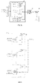
- FIG. 11a is a delay circuit 2000 in a data transmission circuit for reading out the setting parameter MrrData0 from the mode register 200 in response to the mode register read command MrrCmd
- FIG. 11b is a schematic diagram of the working time sequence of FIG. 11a .
- the delay circuit 2000 includes a first flip-flop 501, a second flip-flop 502, a third flip-flop 503, a fourth flip-flop 504, and a delay chain 400.
- the delay chain 400 is configured to generate the first clock signal Clk1, the second clock signal Clk2, the third clock signal Clk3, the fourth clock signal Clk4, and the preset read delay signal Read Latency in response to the mode register read command MrrCmd, wherein the first flip-flop 501 is configured to receive the setting parameter MrrData0 in response to the first clock signal Clk1, and the second flip-flop 502 is configured to receive data provided by the first flip-flop 501 in response to the second clock signal Clk2, the third flip-flop 503 is configured to receive data provided by the second flip-flop 502 in response to the third clock signal Clk3, and the fourth flip-flop 504 is configured to receive data provided by the third flip-flop 503 and output the setting parameter MrrData1 in response to the fourth clock signal Clk4.
- the time of reading out the setting parameter MrrData2 in response to mode register read command is controlled to match the time of reading out the array area data ArrayData in response to the array area data read command ReadCmd.
- FIG. 11a Refer to FIG. 11a and FIG. 11c at the same time.
- Each clock (Clk1, Clk2, Clk3, Clk4) in FIG. 11a needs to be adjusted to ensure the correct timing of MrrData1 to MrrData2.
- FIG. 11c only needs to adjust the timing from MrrCmd to Read Latency, and the technical scheme of FIG. 11c is easier to adjust.
- a storage device including a storage unit array 300, a mode register 200, and any data transmission circuit in the embodiments of the present application; wherein, the storage unit array 300 is configured to store the array area data ArrayData, and the mode register 200 is configured to store the mode register data MrrData0.
- This embodiment realizes the differential control of the mode register data storage unit 1 and the array area data storage unit 3, so that the time of reading out the mode register data MrrData2 in response to the mode register read command matches the time of reading out the array area data ArrayData in response to an array area data read command, so as to accurately control the mode register data MrrData2 and array area data ArrayData to be output through their respective output channels in turn.
- a data transmission method is provided according to an embodiment of the present application, the data transmission method includes:
- a data transmission method including:
- the mode register data processing unit responds to the mode register read command to read out the mode register data from the mode register, and responds to the preset read delay signal to output the mode register data to the mode register data storage unit; based on the mode register data storage unit responding to the first clock signal to output the mode register data, and based on the array area data storage unit being able to respond to the first pointer signal to receive the array area data and respond to the second pointer signal to output the array area data, wherein the output terminal of the array area data storage unit and the output terminal of the mode register data storage unit are both connected to the first node, the differential control of the mode register data storage unit and the array area data storage unit is realized, so that the time of reading out the mode register data in response to the mode register read command matches the time of reading out the array area data in response to the array area data read command, so as to accurately control the mode register data
- the operation delay of the controllable delay module in the present application is determined, it is less affected by changes in the working environment, which can effectively avoid control errors in the data transmission path due to the influence of the working environment; and the operation delay of the controllable delay module can be controlled and adjusted to meet the working parameter requirements of different types of semiconductor storage devices.
- the operation delay of the controllable delay module is determined, it is less affected by changes in the working environment, which can effectively avoid control errors in the data transmission path due to the influence of the working environment; and the operation delay of the controllable delay module can be controlled and adjusted to meet the working parameter requirements of different types of semiconductor storage devices.
- a data transmission method including:
- the mode register data processing unit responds to the mode register read command to read out the mode register data from the mode register, and responds to the preset read delay signal to output the mode register data to the mode register data storage unit; based on the array area data storage unit responding to the first pointer signal to receive the array area data, and responding to the second pointer signal to output the array area data; and based on the mode register data storage unit responding to the first clock signal to output the mode register data; wherein, the output terminal of the array area data storage unit and the output terminal of the mode register data storage unit are both connected to the first node; the differential control of the mode register data storage unit and the array area data storage unit is realized, so that the time of reading out the mode register data in response to the mode register read command matches the time of reading out the array area data in response to the array area data read command, so as to
- FIGS. 12-14 are displayed in sequence as indicated by the arrows, these steps are not necessarily performed in sequence in the order indicated by the arrows. Unless there is a clear description in this application, there is no strict order for the execution of these steps, and these steps can be executed in other orders. Moreover, at least part of the steps in FIG.s 12-14 may include multiple steps or multiple stages. These steps or stages are not necessarily executed at the same time, but can be executed at different times. The order of execution is not necessarily performed sequentially, but may be performed alternately with other steps or at least a part of the steps or stages in other steps.
- Non-volatile memory may include read only memory (ROM), programmable ROM (PROM), electrically programmable ROM (EPROM), electrically erasable programmable ROM (EEPROM), or flash memory.
- Volatile memory may include random access memory (RAM) or external cache memory.
- RAM is available in many forms, such as static RAM (SRAM), dynamic RAM (DRAM), synchronous DRAM (SDRAM), double data rate SDRAM (DDRSDRAM), enhanced SDRAM (ESDRAM), synchronous link (Synchlink) DRAM (SLDRAM), direct memory bus dynamic RAM (DRDRAM), and memory bus dynamic RAM (RDRAM), etc.
- SRAM static RAM
- DRAM dynamic RAM
- SDRAM synchronous DRAM
- DDRSDRAM double data rate SDRAM
- ESDRAM enhanced SDRAM
- SLDRAM synchronous link (Synchlink) DRAM
- DRAM direct memory bus dynamic RAM
- RDRAM memory bus dynamic RAM
Landscapes
- Engineering & Computer Science (AREA)
- Theoretical Computer Science (AREA)
- Physics & Mathematics (AREA)
- General Engineering & Computer Science (AREA)
- General Physics & Mathematics (AREA)
- Microelectronics & Electronic Packaging (AREA)
- Computer Hardware Design (AREA)
- Human Computer Interaction (AREA)
- Databases & Information Systems (AREA)
- Dram (AREA)
- Information Transfer Systems (AREA)
- Communication Control (AREA)
Abstract
Description
- The present application claims the benefit of priority to Chinese patent application
CN202110336625.5 filed with the Chinese Patent Office on March 29, 2021 - The present application relates to, but not limit to a data transmission circuit and method, and a storage device.
- A semiconductor storage device usually includes a storage array area and a peripheral circuit area, wherein the storage array area is provided with a storage unit array including a plurality of storage units; the peripheral circuit area is provided with a control circuit for controlling reading and writing and a mode register for storing mode register data. The mode register data stored in the mode register can be read out by the mode register read command.
- If, on the premise of meeting the working parameter requirements of a specific type of semiconductor storage device, the time of reading out the mode register data in response to the mode register read command is set to match the time of reading out the array area data in response to the array area data read command, so the timing of the transmission path of reading out the mode register data in response to the mode register read command is the same as the timing of the transmission path of reading out the array area data in response to the array area data read command.
- A first aspect of the present application provides a data transmission circuit, including a mode register data storage unit, and an array area data storage unit. The mode register data storage unit is configured to output mode register data in response to a first clock signal. An output terminal of the array area data storage unit and an output terminal of the mode register data storage unit are both connected to a first node. The array area data storage unit is configured to receive array area data in response to a first pointer signal, and is also configured to output the array area data in response to a second pointer signal.
- In the data transmission circuit of the above embodiment, by setting the mode register data storage unit to output the mode register data in response to the first clock signal, and setting that the output terminal of the array area data storage unit and the output terminal of the mode register data storage unit are connected to the first node, and that the array area data storage unit is configured to receive the array area data in response to the first pointer signal and output the array area data in response to the second pointer signal, the differential control of mode register data storage unit and array area data storage unit is realized, so that the time of reading out the mode register data in response to a mode register read command matches the time of reading out the array area data in response to an array area data read command, so as to accurately control the mode register data and array area data to be output through their respective output channels in turn.
- A second aspect of the present application provides a data transmission circuit, including a controllable delay module, a mode register data processing unit, an array area data storage unit, and a mode register data storage unit, wherein the controllable delay module is configured to generate a preset read delay signal in response to a mode register read command; the mode register data processing unit is connected with the controllable delay module, and is configured to read out mode register data from a mode register in response to the mode register read command, and is also configured to output the mode register data to the mode register data storage unit in response to the preset read delay signal; an output terminal of the array area data storage unit and an output terminal of the mode register data storage unit are connected to a first node, and the array area data storage unit is configured to receive array area data in response to a first pointer signal and is also configured to output the array area data in response to a second pointer signal; and the mode register data storage unit is configured to output the mode register data in response to a first clock signal.
- In the data transmission circuit in the above embodiment, by setting the controllable delay module to generate the preset read delay signal in response to the mode register read command, the mode register data processing unit reads out the mode register data from the mode register in response to the mode register read command, and outputs the mode register data to the mode register data storage unit in response to the preset read delay signal; and by setting the mode register data storage unit to output the mode register data in response to the first clock signal, the output terminal of the array area data storage unit and the output terminal of the mode register data storage unit to be both connected to the first node, and the array area data storage unit to receive the array area data in response to the first pointer signal and to output the array area data in response to the second pointer signal, the differential control of mode register data storage unit and array area data storage unit is realized, so that the time of reading out the mode register data in response to the mode register read command matches the time of reading out the array area data in response to an array area data read command, so as to accurately control the mode register data and array area data to be output through their respective output channels in turn. Once the operation delay of the controllable delay module in the present application is determined, it is less affected by changes in the working environment, which can effectively avoid control errors in the data transmission path due to the influence of the working environment; and the operation delay of the controllable delay module can be controlled and adjusted, which can meet the working parameter requirements of different types of semiconductor storage devices.
- A third aspect of the present application provides a data transmission circuit, including: a delay module, a mode register data processing unit, an array area data storage unit, and a mode register data storage unit, wherein the delay module is configured to generate a preset read delay signal, after delaying a first preset time from the moment of receiving a mode register read command; the mode register data processing unit is connected to the delay module, and is configured to read out mode register data from a mode register in response to the mode register read command, and is also configured to output the mode register data to the mode register data storage unit in response to the preset read delay signal; an output terminal of the array area data storage unit and an output terminal of the mode register data storage unit are both connected to a first node and the array area data storage unit is configured to receive array area data in response to a first pointer signal and output the array area data in response to a second pointer signal; and the mode register data storage unit is configured to output the mode register data in response to a first clock signal.
- In the data transmission circuit according to the above embodiment, by setting the delay module to generate the preset read delay signal, after delaying the first preset time from the moment of receiving the mode register read command, the mode register data processing unit reads out the mode register data from the mode register in response to the mode register read command, and outputs the mode register data to the mode register data storage unit in response to the preset read delay signal; and by setting the mode register data storage unit to output the mode register data in response to the first clock signal, the output terminal of the array area data storage unit and the output terminal of the mode register data storage unit to be both connected to the first node, and the array area data storage unit to receive the array area data in response to the first pointer signal and to output the array area data in response to the second pointer signal, the differential control of mode register data storage unit and array area data storage unit is realized, so that the time of reading out the mode register data in response to the mode register read command matches the time of reading out the array area data in response to an array area data read command, so as to accurately control the mode register data and array area data to be output through their respective output channels in turn.
- A fourth aspect of the present application provides a storage device, including a storage unit array, a mode register, and any of the data transmission circuits described in the embodiments of the present application; wherein the storage unit array is configured to store array area data, and the mode register is configured to store mode register data. In this embodiment, the time of reading out the mode register data in response to the mode register read command matches the time of reading out the array area data in response to an array area data read command, so that the timing of the transmission path of reading out the mode register data in response to the mode register read command is the same as the timing of the transmission path of reading out the array area data in response to the array area data read command.
- A fifth aspect of the present application provides a data transmission method, including:
- outputting mode register data based on a mode register data storage unit in response to a first clock signal, and;
- receiving array area data, based on an array area data storage unit in response to a first pointer signal and outputting the array area data, based on the array area data storage unit in response to a second pointer signal, wherein an output terminal of the array area data storage unit and an output terminal of the mode register data storage unit are both connected to a first node.
- A sixth aspect of the present application provides a data transmission method, including:
- generating a preset read delay signal, based on a controllable delay module in response to a mode register read command;
- reading out mode register data from a mode register, based on a mode register data processing unit in response to the mode register read command, and outputting the mode register data to a mode register data storage unit, based on the mode register data processing unit in response to the preset read delay signal;
- outputting the mode register data, based on the mode register data storage unit in response to a first clock signal; and
- receiving array area data, based on an array area data storage unit in response to a first pointer signal, and outputting the array area data, based on the array area data storage unit in response to a second pointer signal, wherein an output terminal of the array area data storage unit and an output terminal of the mode register data storage unit are both connected to a first node.
- A seventh aspect of the present application provides a data transmission method, including:
- generating a preset read delay signal from a delay module, after delaying a first preset time, from the moment when a mode register read command is received;
- reading out mode register data from a mode register, based on a mode register data processing unit in response to the mode register read command, and outputting the mode register data to a mode register data storage unit, based on the mode register data processing unit in response to the preset read delay signal;
- outputting the mode register data, based on the mode register data storage unit in response to a first clock signal; and
- receiving array area data, based on an array area data storage unit in response to a first pointer signal, and outputting the array area data, based on the array area data storage unit in response to a second pointer signal, wherein an output terminal of the array area data storage unit and an output terminal of the mode register data storage unit are both connected to a first node.
- To more clearly describe the technical scheme in the embodiments of the present application, the following will briefly introduce the drawings in the description of the embodiments. It is obvious that the drawings in the following description are only some embodiments of the present application. For those of ordinary skill in the art, other drawings can be obtained based on these drawings without creative work.
-
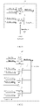
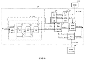
FIG. 1 is a structural block diagram of a data transmission circuit provided according to the first embodiment of the present application; -
FIG. 2 is a structural block diagram of a data transmission circuit provided according to the second embodiment of the present application; -
FIG. 3 is a structural block diagram of a data transmission circuit provided according to the third embodiment of the present application; -
FIG. 4 is a structural block diagram of a data transmission circuit provided according to the fourth embodiment of the present application; -
FIG. 5a is a structural block diagram of a data transmission circuit provided according to a fifth embodiment of the present application; -
FIG. 5b is a structural block diagram of a data transmission circuit provided according to the sixth embodiment of the present application; -
FIG. 6 is a structural block diagram of a first-in first-out data processing unit in a data transmission circuit provided according to an embodiment of the present application; -
FIG. 7 is a structural block diagram of a first-in first-out data processing unit in a data transmission circuit provided according to another embodiment of the present application; -
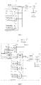
FIG. 8a is a structural block diagram of a data transmission circuit provided according to a seventh embodiment of the present application; -
FIG. 8b is a structural block diagram of a data transmission circuit provided according to the eighth embodiment of the present application; -
FIG. 8c is a structural block diagram of a data transmission circuit provided according to the ninth embodiment of the present application; -
FIG. 8d is a structural block diagram of an array area data storage unit in a data transmission circuit provided according to an embodiment of the present application; -
FIG. 8e is a structural block diagram of a data transmission circuit provided according to the tenth embodiment of the present application; -
FIG. 8f is a structural block diagram of a data transmission circuit provided according to the eleventh embodiment of the present application; -
FIG. 8g is a schematic diagram of an embodiment ofFIG. 8f ; -
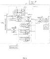
FIG. 9a is a structural block diagram of a data transmission circuit provided according to a twelfth embodiment of the present application; -
FIG. 9b is a structural block diagram of a data transmission circuit provided according to the thirteenth embodiment of the present application; -
FIG. 9c is a structural block diagram of a data transmission circuit provided according to the fourteenth embodiment of the present application; -
FIG. 9d is a structural block diagram of a data transmission circuit provided according to the fifteenth embodiment of the present application; -
FIG. 9e is a structural block diagram of a data transmission circuit provided according to the sixteenth embodiment of the present application; -
FIG. 9f is a schematic diagram of an embodiment ofFIG. 9e ; -
FIG. 10a is a schematic diagram of a response timing sequence of a data transmission circuit to a read command according to an embodiment of the present application; -
FIG. 10b is a schematic diagram of a working sequence of a data transmission circuit provided according to an embodiment of the present application; -
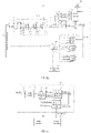
FIG. 11a is a structural block diagram of a delay circuit for responding to a mode register read command; -
FIG. 11b is a schematic diagram of the working time sequence ofFIG. 11a ; -
FIG. 11c is a block diagram of another delay circuit for responding to mode register read commands; -
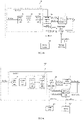
FIG. 12 is a schematic flowchart of a data transmission method provided according to an embodiment of the present application; -
FIG. 13 is a schematic flowchart of a data transmission method provided according to another embodiment of the present application; and -
FIG. 14 is a schematic flowchart of a data transmission method provided according to another embodiment of the present application. - 100. Data transmission circuit; 1. Mode register data storage unit; 3. Array area data storage unit; 4. Delay module; 31. First storage unit; 10. Controllable delay module; 20. Mode register data processing unit; 200. Mode register; 11. Reference delay unit; 12. Controllable delay unit; 121. Delay unit; 122. First controllable switch unit; 41. First delay unit; 42. Second delay unit; 43. Third delay unit; 431. The first sub-delay unit; 432. The second sub-delay unit; 1101. The first read operation delay unit; 1201. The column selection control module; 1301. The third read operation delay unit; 21. The first-in first-out pointer processing unit; 22. First-in first-out data processing unit; 23. Mode register read command processing unit; 221. Second storage unit; 2211. Storage sub-unit; 2212. Driver; 30. Command decoding circuit; 40. Array area data processing unit; 300. Storage unit array; 50. First selector; 51. First-in first-out storage unit; 52. Selection module; 511. Third storage unit; 60. First-in first-out memory; 70. Serial-to-parallel conversion circuit; 80. Data driving module; 90. Data terminal; 501. First flip-flop; 502. Second flip-flop; 503. Third flip-flop; 504. Fourth flip-flop; 400. Delay chain; 1000. Storage device; and 2000. Delay circuit.
- In order to facilitate the understanding of the present application, the following will make a more comprehensive description of the present application with reference to the relevant drawings. The preferred embodiment of the present application is shown in the accompanying drawings. However, the present application can be implemented in many different forms and is not limited to the embodiments described herein. On the contrary, the purpose of providing these embodiments is to make the disclosure of the present application more thorough and comprehensive.
- Unless otherwise defined, all technical and scientific terms used herein have the same meaning as commonly understood by those skilled in the technical field of the present application. The terminology used in the specification of the present application herein is only for the purpose of describing specific embodiments, and is not intended to limit the present application.
- In addition, certain terms used throughout the specification and the following claims refer to specific elements. Those skilled in the art will understand that manufacturers can refer to components with different names. The present application does not intend to distinguish between components with different names but the same function. In the following description and embodiments, the terms "including" and "include" are used openly, and therefore should be interpreted as "including, but not limited to...". Likewise, the term "connected" is intended to express an indirect or direct electrical connection. Correspondingly, if one device is connected to another device, the connection can be done through a direct electrical connection, or through an indirect electrical connection between the other equipment and the connector.
- It should be understood that although the terms "first", "second", etc. may be used herein to describe various elements, these elements should not be limited by these terms. These terms are only used to distinguish one element from another element. For example, without departing from the scope of the present application, the first element may be referred to as the second element, and similarly, the second element may be referred to as the first element.
- Please refer to
FIG. 1 , in an embodiment of the present application, adata transmission circuit 100 is provided, including a mode registerdata storage unit 1 and an array areadata storage unit 3. The mode registerdata storage unit 1 is configured to output the mode register data MrrData2 in response to a first clock signal MrrClk; the output terminal of the array areadata storage unit 3 and the output terminal of the mode registerdata storage unit 1 are both connected to the first node A, and the array areadata storage unit 3 is configured to receive the array area data ArrayData in response to the first pointer signal FifoIn_array, and output the array area data ArrayData in response to the second pointer signal FifoOut_array. - As an example, please continue to refer to
FIG. 1 , by setting the mode registerdata storage unit 1 to output the mode register data MrrData2 in response to the first clock signal MrrClk, wherein before the mode registerdata storage unit 1 outputs the mode register data MrrData2 in response to the first clock signal MrrClk, the mode registerdata storage unit 1 reads the mode register data MrrData1 from the previous data line; then setting the output terminal of the array areadata storage unit 3 and the output terminal of the mode registerdata storage unit 1 to be both connected to the first node A, and the array areadata storage unit 3 to receive the array area data ArrayData in response to the first pointer signal FifoIn_array, and to output the array area data ArrayData in response to the second pointer signal FifoOut_array; the differential control of the mode registerdata storage unit 1 and the array areadata storage unit 3 is realized, so that the time of reading out the mode register data MrrData2 in response to a mode register read command matches the time of reading out the array area data ArrayData in response to an array area data read command, and accurately control the mode register data MrrData and the array area data ArrayData to be output through the respective output channels in turn. The MrrData1 and MrrData2 here can be the same or can match a preset algorithm. - Further, referring to
FIG. 2 , in an embodiment of the present application, the array areadata storage unit 3 includes eightfirst storage units 31, and the output terminal of eachfirst storage unit 31 is connected to the first node A, and the input terminal of eachfirst storage unit 31 is connected to the first data signal line ArrayDataL, wherein, the first data signal line ArrayDataL is used to transmit the array area data ArrayData, so as to realize the accurate control of the transmission of the array area data ArrayData. - Further, continue to refer to
FIG. 2 , in an embodiment of the present application, the driving clock frequency of the first pointer signal FifoIn_array is the same as the driving clock frequency of the second pointer signal FifoOut_array, so as to set the transmission rate of the input data and output data of the array areadata storage unit 3 to be consistent, and realize the data in and out at the same time. - Further, referring to
FIG. 3 , in an embodiment of the present application, thedata transmission circuit 100 further includes a serial-to-parallel conversion circuit 70 and adata driving module 80. The input terminal of the serial-to-parallel conversion circuit 70 is connected to the first node A; thedata driving module 80 is connected to the output terminal of the serial-to-parallel conversion circuit 70, and is used to output the mode register data MrrData2 or the array area data ArrayData. By using the serial-to-parallel conversion circuit 70 to convert the received data into serial data and then provide the serial data to thedata driving module 80 for output, it is convenient to improve the efficiency of data transmission. - Further, referring to
FIG. 4 , in an embodiment of the present application, thedata transmission circuit 100 further includes a mode registerdata processing unit 20. The mode registerdata processing unit 20 includes a first-in first-outpointer processing unit 21, a first-in first-outdata processing unit 22 and a mode register readcommand processing unit 23; wherein the first-in first-outpointer processing unit 21 is configured to generate a third pointer signal MrFifoIn and a fourth pointer signal MrFifoOut in response to the mode register read command MrrCmd; the first-in first-outdata processing unit 22 is connected to both the first-in first-outpointer processing unit 21 and the mode registerdata storage unit 1, and the first-in first-outdata processing unit 22 is configured to read out the mode register data MrrData0 from themode register 200 in response to the third pointer signal MrFifoIn, and is also configured to output the mode register data MrrData1 to the mode registerdata storage unit 1 in response to the fourth pointer signal MrFifoOut; and the mode register readcommand processing unit 23 is configured to generate the first clock signal MrrClk according to the received mode register read command MrrCmd, the second clock signal Clk, and the preset read delay signal Read Latency. By controlling the time when the mode register data MrrData1 is output through the mode registerdata storage unit 1, according to the mode register read command MrrCmd, the second clock signal Clk and the preset read delay signal Read Latency, it can accurately control the mode register data MrrData0 and the array area data ArrayData to be output through their respective data output channels in turn. The MrrData0 and MrrData1 here can be the same or can match a preset algorithm. - As an example, please continue to refer to
FIG. 4 , in an embodiment of the present application, the driving clock frequency of the third pointer signal MrFifoIn is the same as the driving clock frequency of the fourth pointer signal MrFifoOut, so as to accurately control the time difference between the read data and the output data of the first-in first-outdata processing unit 22. - Further, referring to
FIGS. 5a and5b , in an embodiment of the present application, thedata transmission circuit 100 further includes acommand decoding circuit 30 and an array area data processing unit. The first output terminal of thecommand decoding circuit 30 is connected to both the input terminal of the mode register readcommand processing unit 23 and the input terminal of the first-in first-outpointer processing unit 21, and thecommand decoding circuit 30 is configured to receive the read command Read, decode the read command Read and determine whether the read command is the mode register read command MrrCmd. If so, the mode register read command MrrCmd is output, otherwise, the array area data read command ReadCmd is generated. The input terminal of the array areadata processing unit 40 is connected to the second output terminal of thecommand decoding circuit 30, and the array areadata processing unit 40 is configured to read out the array area data ArrayData from thestorage unit array 300, in response to the array area data read command ReadCmd,and provide the array area data ArrayData to the array areadata storage unit 3. In this embodiment, the mode register data MrrData2 and the array area data ArrayData are read out via adata transmission circuit 100, as opposed to reading out the mode register data MrrData and array area data ArrayData through different data transmission paths. - As an example shown in
FIG. 5b , in an embodiment of the present application, theselection module 52 is configured to receive the mode register data MrrData1 and the array area data ArrayData; and the output terminal of theselection module 52 is connected to the first-in first-out storage unit 51; the first-in first-out storage unit 51 includes jthird storage units 511 connected in parallel, j is a positive integer, and j can be set to be equal to the bit width of the array area data ArrayData. The mode register data MrrData1 and the array area data ArrayData are sequentially output through the first-in first-out storage unit 51, the serial-to-parallel conversion circuit 70, thedata driving module 80 and thedata terminal 90 by controlling the switching of theselection module 52. Referring toFIG. 5a andFIG. 5b at the same time, the mode register data MrrData0 and the array area data ArrayData inFIG. 5a are transmitted to the serial-to-parallel conversion circuit 70 through different FIFOs (first-in first-out registers); the mode register data MrrData0 and the array area data ArrayData inFIG. 5b are transmitted to the serial-to-parallel conversion circuit 70 through the same FIFO. The technical scheme ofFIG. 5a is more flexible for the timing control of the data transmission circuit, and the technical scheme ofFIG. 5b can make the area of the data transmission circuit smaller. - As an example shown in
FIG. 6 , in an embodiment of the present application, the first-in first-outdata processing unit 22 includes asecond storage unit 221, and the output terminal of eachsecond storage unit 221 is connected to the second node O; thesecond storage unit 221 includes astorage subunit 2211 and adriver 2212, the input terminal of thedriver 2212 is connected to the output terminal of thestorage subunit 2211; thestorage subunit 2211 is driven by the third pointer signal MrFifoIn to receive the mode register data MrrDataO; and thedriver 2212 is driven by the fourth pointer signal MrFifoOut to output the mode register data MrrData1. So as to make the first-in first-outdata processing unit 22 cooperate with the first-in first-outpointer processing unit 21 to achieve the accurate control of the time of reading out the mode register data MrrData1 in response to the mode register read command MrrCmd, thereby the time of reading out the moderegister data MrrData 1 in response to the mode register read command MrrCmd can be accurately controlled to match the time of reading out the array area data ArrayData in response to the array area data read command ReadCmd. - As an example, please refer to
FIG. 7 , in an embodiment of the present application, the data input terminal of eachstorage subunit 2211 is connected to themode register 200, so that eachstorage subunit 2211 reads out the mode register data MrrData0 from themode register 200 in response to the third pointer signal MrFifoIn, eachdriver 2212 outputs the mode register data MrrData1 in response to the fourth pointer signal MrFifoOut. - As an example shown in
FIG. 7 , in an embodiment of the present application, the driving clock frequency of the third pointer signal MrFifoIn and the driving clock frequency of the fourth pointer signal MrFifoOut are the same, so as to accurately control the time difference between the read data and the output data of the first-in first-outdata processing unit 22. - Referring to
FIG. 8a , in an embodiment of the present application, adata transmission circuit 100 is provided, including acontrollable delay module 10, a mode registerdata processing unit 20, an array areadata storage unit 3, and a mode registerdata storage unit 1. Thecontrollable delay module 10 is configured to generate a preset read delay signal Read Latency in response to the mode register read command MrrCmd; the mode registerdata processing unit 20 is connected to the controllable delay module, and the mode registerdata processing unit 20 is configured to read out the mode register data MrrData0 from themode register 200 in response to the mode register read command MrrCmd, and is also configured to output the mode register data MrrData1 to the mode registerdata storage unit 1 in response to the preset read delay signal Read Latency; the output terminal of the array areadata storage unit 3 and the output terminal of the mode registerdata storage unit 1 are both connected to the first node A, and the array areadata storage unit 3 is configured to receive array area data ArrayData in response to the first pointer signal FifoIn_array, and is also configured to output the array area data ArrayData in response to the second pointer signal FifoOut_array; and the mode registerdata storage unit 1 is configured to output the mode register data MrrData2 in response to the first clock signal MrrClk. - As an example, please continue to refer to
FIG. 8a , by setting the controllable delay module 10 to generate the preset read delay signal Read Latency in response to the mode register read command MrrCmd, the mode register data processing unit 20 reads out the mode register data MrrData0 from the mode register 200 in response to the mode register read command MrrCmd, and outputs the mode register data MrrData1 to the mode register data storage unit 1 in response to the preset read delay signal Read Latency; and by setting the mode register data storage unit 1 to output the mode register data MrrData2 in response to the first clock signal MrrClk, the output terminal of the array area data storage unit 3 and the output terminal of the mode register data storage unit 1 to be both connected to the first node A, and the array area data storage unit 3 to receive the array area data ArrayData in response to the first pointer signal FifoIn_array, and to output the array area data ArrayData in response to the second pointer signal FifoOut_array, the differential control of the mode register data storage unit 1 and the array area data storage unit 3 is realized, so that the time of reading out the mode register data MrrData2 in response to the mode register read command MrrCmd matches the time of reading out the array area data ArrayData in response to the array area data read command ReadCmd, so as to accurately control the mode register data MrrData2 and array area data ArrayData to be output through their respective output channels in turn. Once the operation delay of thecontrollable delay module 10 in the present application is determined, it is less affected by changes in the working environment, which can effectively avoid control errors in the data transmission path due to the influence of the working environment; and the operation delay of thecontrollable delay module 10 can control and adjust to meet the working parameter requirements of different types of semiconductor storage devices. - As an example, please continue to refer to
FIG. 8a , in an embodiment of the present application, the time difference between the starting time when the mode registerdata processing unit 20 outputs the mode register data MrrData1 and the time when thecontrollable delay module 10 receives the mode register read command MrrCmd is the first preset threshold, so that the time of reading out the mode register data MrrData1 in response to the mode register read command MrrCmd matches the time of reading out the array area data ArrayData in response to the array area data read command ReadCmd. - Further, referring to
FIG. 8b , in an embodiment of the present application, thecontrollable delay module 10 includes areference delay unit 11 and acontrollable delay unit 12. Thereference delay unit 11 is configured to generate an initial preset read delay signal Read Latency in response to the mode register read command MrrCmd; thecontrollable delay unit 12 is connected to the output terminal of thereference delay unit 11 and the input terminal of the mode registerdata processing unit 20, and thecontrollable delay unit 12 is configured to generate a preset read delay signal Read Latency after delaying the preset delay time from the moment of receiving the initial preset read delay signal Read Latency, wherein, the sum of the operation delay of thecontrollable delay unit 12 and the operation delay of thereference delay unit 11 is equal to the first preset threshold. By setting the sum of the operation delay of thereference delay unit 11 and the operation delay of thecontrollable delay unit 12 to be equal to the first preset threshold, the operation delay range of thecontrollable delay unit 12 is reduced to improve the efficiency and accuracy of adjusting the operation delay of thecontrollable delay module 10 to the first preset threshold. - Further, referring to
FIG. 8c , in an embodiment of the present application, thecontrollable delay unit 10 includes threedelay units 121 connected in series; wherein, twodelay units 121 each are connected in parallel with a firstcontrollable switch unit 122; wherein by controlling the on and off of each firstcontrollable switch unit 122, the number of thedelay units 121 in thecontrollable delay unit 12 connected in series between thereference delay unit 11 and the mode registerdata processing unit 20 is changed to adjust the operation delay of thecontrollable delay unit 12, so as to realize the gradient control of the operation delay of thecontrollable delay unit 12, to improve the efficiency and accuracy of adjusting the operation delay of thecontrollable delay module 10 to the first preset threshold. - As an example, please refer to
FIG. 8d , in an embodiment of the present application, the array areadata storage unit 3 includes a plurality offirst storage units 31, and the output terminal of eachfirst storage unit 31 is connected to the first node A, the input terminal of eachfirst storage unit 31 is connected to the first data signal line ArrayDataL, and the first data signal line ArrayDataL is used to transmit the array area data ArrayData, so as to realize the accurate control of the transmission of the array area data ArrayData. - As an example, please continue to refer to
FIG. 8d , in an embodiment of the present application, the driving clock frequency of the first pointer signal FifoIn_array and the driving clock frequency of the second pointer signal FifoOut_array are the same, so as to set the transmission rate of the input data and the output data of the array areadata storage unit 3 to be consistent, and realize the data in and out at the same time. - Further, referring to
FIG. 8e , in an embodiment of the present application, the mode registerdata processing unit 20 includes a first-in first-outpointer processing unit 21, a first-in first-outdata processing unit 22, and a mode register readcommand processing unit 23. The mode register readcommand processing unit 23 is configured to generate the first clock signal MrrClk according to the received mode register read command MrrCmd, the second clock signal Clk and the preset read delay signal Read Latency; the first-in first-outpointer processing unit 21 is configured to generate the third pointer signal MrFifoIn and the fourth pointer signal MrFifoOut in response to the mode register read command MrrCmd; the first-in first-outdata processing unit 22 is connected with the first-in first-outpointer processing unit 21 and the mode registerdata storage unit 1, and the first-in first-outdata processing unit 22 is configured to read out the mode register data MrrData0 from themode register 200 in response to the third pointer signal MrFifoIn, and is also configured to output the mode register data MrrData1 to the mode registerdata storage unit 1 in response to the fourth pointer signal MrFifoOut. - As an example, please continue to refer to
FIG. 8e , in an embodiment of the present application, the driving clock frequency of the third pointer signal MrFifoIn and the driving clock frequency of the fourth pointer signal MrFifoOut are the same, so as to accurately control the time difference between the read data and the output data of the first-in first-outdata processing unit 22. - Further, referring to
FIG. 8f , in an embodiment of the present application, thedata transmission circuit 100 further includes acommand decoding circuit 30 and an array areadata processing unit 40, wherein a first output terminal of thecommand decoding circuit 30 is connected to the input terminal of the mode register readcommand processing unit 23 and the input terminal of the first-in first-outpointer processing unit 21, and thecommand decoding circuit 30 is configured to receive the read command, decode the read command Read and determine whether the read command Read is the mode register read command MrrCmd. If so, the mode register read command MrrCmd is output, otherwise, the array area data read command ReadCmd is generated. The input terminal of the array areadata processing unit 40 is connected to a second output terminal of thecommand decoding circuit 30, and the array areadata processing unit 40 is configured to read out the array area data ArrayData from thestorage unit array 300 in response to the array area data read command ReadCmd to provide the array area data ArrayData to the array areadata storage unit 3. - As an example, please refer to
FIG. 8g . It can be set that thereference delay unit 11 includes several sub-delay units connected in series, wherein the sub-delay units can be used to copy the operation delay of the functional unit with fixed delay time in the path of array area data read out by the array areadata processing unit 40 in response to the array area data read command, and set the delay time of the operation delay of the controllable delay unit to match the delay time of the functional unit with variable delay time in the path of the array area data read out by the array areadata processing unit 40 in response to the array area data reading command, so as to realize the gradient control of the operation delay of the controllable delay unit, to improve the efficiency and accuracy of adjusting the operation delay of the controllable delay module to the first preset threshold.. - Please refer to
FIG. 9a . In an embodiment of the present application, adata transmission circuit 100 is provided, which includes adelay module 4, a mode registerdata processing unit 20, an array areadata storage unit 3, and a mode registerdata storage unit 1. Thedelay module 4 is configured to generate a preset read delay signal Read Latency, after delaying a first preset time from the moment of receiving the mode register read command MrrCmd; the mode registerdata processing unit 20 is connected to thedelay module 4 and the mode registerdata storage unit 1, and is configured to read out the mode register data MrrData0 from themode register 200 in response to the mode register read command MrrCmd, and is also configured to output the mode register data MrrData1 to the mode registerdata storage unit 1 in response to the preset read delay signal Read Latency; and the output terminal of the array areadata storage unit 3, and the output terminal of the mode registerdata storage unit 1 are both connected to the first node A, and the array areadata storage unit 3 is configured to receive the array area data ArrayData in response to the first pointer signal FifoIn_array, and is also configured to output the array area data ArrayData in response to the second pointer signal FifoOut_array; wherein the mode registerdata storage unit 1 is configured to output the mode register data MrrData2 in response to the first clock signal MrrClk. - As an example, please refer to
FIG. 9a , by setting the delay module 4 to generate the preset read delay signal Read Latency, after delaying the first preset time from the moment of receiving the mode register read command MrrCmd, the mode register data processing unit 20 reads out the mode register data MrrData0 from the mode register 200 in response to the mode register read command MrrCmd, and outputs the mode register data MrrData1 to the mode register data storage unit 1 in response to the preset read delay signal Read Latency; and by setting the mode register data storage unit 1 to output the mode register data MrrData2 in response to the first clock signal MrrClk, the output terminal of the array area data storage unit 3 and the output terminal of the mode register data storage unit 1 to be both connected to the first node, and the array area data storage unit 3 to receive the array area data ArrayData in response to the first pointer signal FifoIn_array and to output the array area data ArrayData in response to the second pointer signal FifoOut_array, the differential control of the mode register data storage unit 1 and array area data storage unit 3 is realized, so that the time of reading out the mode register data MrrData2 in response to the mode register read command MrrCmd matches the time of reading out the array area data ArrayData in response to an array area data read command ReadCmd, so as to accurately control the mode register data MrrData2 and array area data ArrayData to be output through their respective output channels in turn. - Further, referring to
FIG. 9b , in an embodiment of the present application, thedelay module 4 includes afirst delay unit 41, asecond delay unit 42, and athird delay unit 43. Thefirst delay unit 41 is configured to generate a first preset read delay signal, after delaying a second preset time from the moment of receiving the mode register read command MrrCmd; thesecond delay unit 42 is connected to the output terminal of thefirst delay unit 41, and is configured to generate a second preset read delay signal, after delaying a third preset time from the moment of receiving the first preset read delay signal, and the third preset time is equal to the operation delay of the column selection control module (not shown); thethird delay unit 43 is connected to the output terminal of thesecond delay unit 42 and the input terminal of the mode register data processing unit 20and is configured to generate a preset read delay signal Read Latency, after delaying a fourth preset time from the moment of receiving the second preset read delay signal; wherein, the sum of the second preset time, the third preset time, and the fourth preset time is equal to the first preset time. This embodiment can avoid the influence of the operation delay of the column selection control module in a specific type of semiconductor storage device on the transmission circuit. - Further, please refer to
FIG. 9c , in an embodiment of the present application, thethird delay unit 43 includes a firstsub-delay unit 431 and a secondsub-delay unit 432. The firstsub-delay unit 431 is connected to the output terminal of thesecond delay unit 42, and is configured to generate a third preset read delay signal, after delaying a fifth preset time from the moment of receiving the second preset read delay signal, and the fifth preset time is equal to the operation delay of the read-write amplifier; the secondsub-delay unit 432 is connected to the output terminal of the firstsub-delay unit 431 and the input terminal of the mode registerdata processing unit 20, and is configured to generate the preset read delay signal Read Latency, after delaying a sixth preset time from the moment of receiving the third preset read delay signal; wherein the sum of the fifth preset time and the sixth preset time is equal to the fourth preset time. This embodiment can avoid the influence of the operation delay of the read-write amplifier in a specific type of semiconductor storage device on the transmission circuit. - As an example, please continue to refer to
FIG. 9c , in an embodiment of the present application, the array areadata storage unit 3 includes a plurality of first storage units 31 (not shown inFIG. 9c ), wherein the output terminal of eachfirst storage unit 31 is connected to the first node A, the input terminal of eachfirst storage unit 31 is connected to the first data signal line, and the first data signal line is used to transmit array area data ArrayData. - As an example, please continue to refer to
FIG. 9c , in an embodiment of the present application, the driving clock frequency of the first pointer signal FifoIn_array and the driving clock frequency of the second pointer signal FifoOut_array are the same. - Further, referring to
FIG. 9d , in an embodiment of the present application, the mode registerdata processing unit 20 includes a first-in first-outpointer processing unit 21, a first-in first-outdata processing unit 22, and a mode register readcommand processing unit 23. The mode register readcommand processing unit 23 is configured to generate the first clock signal MrrClk according to the received mode register read command MrrCmd, the second clock signal Clk and the preset read delay signal Read Latency; the first-in first-outpointer processing unit 21 is configured to generate the third pointer signal MrFifoIn and the fourth pointer signal MrFifoOut in response to the mode register read command MrrCmd; the first-in first-outdata processing unit 22 is connected with the first-in first-outpointer processing unit 21 and the mode registerdata storage unit 1, and is configured to read out the mode register data MrrData0 from themode register 200 in response to the third pointer signal MrFifoIn, and is also configured to output the mode register data MrrData1 to the mode registerdata storage unit 1 in response to the fourth pointer signal MrFifoOut. In an embodiment of the present application, the driving clock frequency of the third pointer signal MrFifoIn and the driving clock frequency of the fourth pointer signal MrFifoOut are the same. - Further, please refer to
FIGS. 9e and9f , in an embodiment of the present application, thedata transmission circuit 100 further includes acommand decoding circuit 30 and an array areadata processing unit 40, a first output terminal of thecommand decoding circuit 30 is connected to both an input terminal of the mode register readcommand processing unit 23 and an input terminal of the first-in first-outpointer processing unit 21, and thecommand decoding circuit 30 is configured to receive the read command, decode the read command Read and determine whether the read command Read is the mode register read command MrrCmd. If so, the mode register read command MrrCmd is output, otherwise, the array area data read command ReadCmd is generated. The input terminal of the array area data processing unit is connected to the second output terminal of thecommand decoding circuit 30, and the array area data processing unit is configured to read out the array area data ArrayData from thestorage unit array 300, in response to the array area data read command ReadCmd, and provide the array area data ArrayData to the array areadata storage unit 3. - As an example, please continue to refer to
FIG. 9f , the delay time of the array area data read out by the array areadata processing unit 40 in response to the array area data read command can be equivalent to the sum of the delay time of the first readoperation delay unit 1101 and the operation delay of columnselection control module 1201 and the delay time of the third readoperation delay unit 1301. By setting thesecond delay unit 12 to copy the operation delay of the columnselection control module 1201, setting the delay time of thefirst delay unit 11 to match the delay time of the first readoperation delay unit 1101, and setting the delay time of the third delay unit 13 to match the delay time of the third readoperation delay unit 1301, so that the time of reading out the setting parameter MrrData2 in response to the mode register read command MrrCmd matches the time of reading out the array area data in response to the array area data read command. - Further, please continue to refer to
FIG. 7 , in an embodiment of the present application, the difference between the operation delay of the array areadata processing unit 40 and the first preset time can be set as a preset threshold, so as to meet the working parameter requirements of specific types of semiconductor storage devices, such as dynamic random access memory (DRAM). - As an example, please refer to
FIG. 10a and FIG. 10b , in an embodiment of the present application, the third pointer signal MrFifoIn can be set to have the same frequency as the mode register read command MrrCmd, the fourth pointer signal MrFifoOut can be set to have the same frequency as the preset read delay signal Read Latency,. the time difference between the driving time of the preset read delay signal Read Latency and the driving time of the mode register read command MrrCmd is set to be the first preset time Td, and the difference between the operation delay of the array areadata processing unit 40 and the first preset time is set to be the preset threshold, so that the time of reading out the setting parameter MrrData2 in response to the mode register read command MrrCmd matches the time of reading out the array area data ArrayData in response to the array area data read command ReadCmd. - As an example, in an embodiment of the present application, the preset threshold may be set to an integer multiple of the column refresh cycle to meet the working parameter requirements of specific types of semiconductor storage devices, such as LPDDR4.
-
FIG. 11a is adelay circuit 2000 in a data transmission circuit for reading out the setting parameter MrrData0 from themode register 200 in response to the mode register read command MrrCmd, andFIG. 11b is a schematic diagram of the working time sequence ofFIG. 11a . Thedelay circuit 2000 includes a first flip-flop 501, a second flip-flop 502, a third flip-flop 503, a fourth flip-flop 504, and adelay chain 400. Thedelay chain 400 is configured to generate the first clock signal Clk1, the second clock signal Clk2, the third clock signal Clk3, the fourth clock signal Clk4, and the preset read delay signal Read Latency in response to the mode register read command MrrCmd, wherein the first flip-flop 501 is configured to receive the setting parameter MrrData0 in response to the first clock signal Clk1, and the second flip-flop 502 is configured to receive data provided by the first flip-flop 501 in response to the second clock signal Clk2, the third flip-flop 503 is configured to receive data provided by the second flip-flop 502 in response to the third clock signal Clk3, and the fourth flip-flop 504 is configured to receive data provided by the third flip-flop 503 and output the setting parameter MrrData1 in response to the fourth clock signal Clk4. By controlling the driving time of the first clock signal Clk1, the second clock signal Clk2, the third clock signal Clk3, the fourth clock signal Clk4, and the preset read delay signal Read Latency generated by thedelay chain 400, the time of reading out the setting parameter MrrData2 in response to mode register read command is controlled to match the time of reading out the array area data ArrayData in response to the array area data read command ReadCmd. - Refer to
FIG. 11a and FIG. 11c at the same time. Each clock (Clk1, Clk2, Clk3, Clk4) inFIG. 11a needs to be adjusted to ensure the correct timing of MrrData1 to MrrData2. In comparison,FIG. 11c only needs to adjust the timing from MrrCmd to Read Latency, and the technical scheme ofFIG. 11c is easier to adjust. - In an embodiment of the present application, a storage device is provided, including a
storage unit array 300, amode register 200, and any data transmission circuit in the embodiments of the present application; wherein, thestorage unit array 300 is configured to store the array area data ArrayData, and themode register 200 is configured to store the mode register data MrrData0. This embodiment realizes the differential control of the mode registerdata storage unit 1 and the array areadata storage unit 3, so that the time of reading out the mode register data MrrData2 in response to the mode register read command matches the time of reading out the array area data ArrayData in response to an array area data read command, so as to accurately control the mode register data MrrData2 and array area data ArrayData to be output through their respective output channels in turn. - Referring to
FIG. 12 , a data transmission method is provided according to an embodiment of the present application, the data transmission method includes: - Step 502: outputting the mode register data based on the mode register data storage unit in response to the first clock signal; and
-
Step 504, receiving the array area data based on the array area data storage unit in response to the first pointer signal and outputting the array area data based on the array area data storage unit in response to the second pointer signal, wherein the output terminal of the array area data storage unit and the output terminal of the mode register data storage unit are both connected to the first node. - As an example, please continue to refer to
FIG. 12 , by outputting the mode register data based on the mode register data storage unit in response to the first clock signal, and receiving the array area data based on the array area data storage unit in response to the first pointer signal and outputting the array area data based on the array area data storage unit in response to the second pointer signal, wherein the output terminal of the array area data storage unit and the output terminal of the mode register data storage unit are both connected to the first node, the differential control of the mode register data storage unit and the array area data storage unit is realized, so that the time of reading out the mode register data in response to the mode register read command matches the time of reading out the array area data in response to the array area data read command, so as to accurately control the mode register data and the array area data to be output through their respective output channels in turn. - Please refer to
FIG. 13 , in an embodiment of the present application, a data transmission method is provided, including: - Step 602: generating a preset read delay signal, based on the controllable delay module in response to the mode register read command;
- Step 604: reading out the mode register data from the mode register based on the mode register data processing unit in response to the mode register read command, and outputting the mode register data to the mode register data storage unit based on the mode register data processing unit in response to the preset read delay signal;
- Step 606: outputting the mode register data, based on the mode register data storage unit in response to the first clock signal; and
- Step 608: receiving the array area data, based on the array area data storage unit in response to the first pointer signal, and outputting the array area data, based on the array area data storage unit in response to the second pointer signal, wherein the output terminal of the array area data storage unit and the output terminal of the mode register data storage unit are both connected to the first node.
- As an example, please continue to refer to
FIG. 13 , based on the controllable delay module responding to the mode register read command to generate the preset read delay signal, so that the mode register data processing unit responds to the mode register read command to read out the mode register data from the mode register, and responds to the preset read delay signal to output the mode register data to the mode register data storage unit; based on the mode register data storage unit responding to the first clock signal to output the mode register data, and based on the array area data storage unit being able to respond to the first pointer signal to receive the array area data and respond to the second pointer signal to output the array area data, wherein the output terminal of the array area data storage unit and the output terminal of the mode register data storage unit are both connected to the first node, the differential control of the mode register data storage unit and the array area data storage unit is realized, so that the time of reading out the mode register data in response to the mode register read command matches the time of reading out the array area data in response to the array area data read command, so as to accurately control the mode register data and the array area data to output through their respective output channels in turn. Once the operation delay of the controllable delay module in the present application is determined, it is less affected by changes in the working environment, which can effectively avoid control errors in the data transmission path due to the influence of the working environment; and the operation delay of the controllable delay module can be controlled and adjusted to meet the working parameter requirements of different types of semiconductor storage devices. Once the operation delay of the controllable delay module is determined, it is less affected by changes in the working environment, which can effectively avoid control errors in the data transmission path due to the influence of the working environment; and the operation delay of the controllable delay module can be controlled and adjusted to meet the working parameter requirements of different types of semiconductor storage devices. - Referring to
FIG. 14 , in an embodiment of the present application, a data transmission method is provided, including: -
Step 702, after delaying a first preset time from the moment of receiving the mode register read command, the delay module generating a preset read delay signal; -
Step 704, reading out the mode register data from the mode register, based on the mode register data processing unit in response to the mode register read command, and outputting the mode register data to the mode register data storage unit, based on the mode register data processing unit in response to the preset read delay signal; - Step 706: outputting the mode register data, based on the mode register data storage unit in response to the first clock signal, and
-
Step 708, receiving the array area data, based on the array area data storage unit in response to the first pointer signal, and outputting the array area data, based on the array area data storage unit in response to the second pointer signal, wherein the output terminal of the array area data storage unit and the output terminal of the mode register data storage unit are both connected to the first node. - As an example, please continue to refer to
FIG. 14 , based on the delay module generating the preset read delay signal after delaying the first preset time from the moment of receiving the mode register read command; so that the mode register data processing unit responds to the mode register read command to read out the mode register data from the mode register, and responds to the preset read delay signal to output the mode register data to the mode register data storage unit; based on the array area data storage unit responding to the first pointer signal to receive the array area data, and responding to the second pointer signal to output the array area data; and based on the mode register data storage unit responding to the first clock signal to output the mode register data; wherein, the output terminal of the array area data storage unit and the output terminal of the mode register data storage unit are both connected to the first node; the differential control of the mode register data storage unit and the array area data storage unit is realized, so that the time of reading out the mode register data in response to the mode register read command matches the time of reading out the array area data in response to the array area data read command, so as to accurately control the mode register data and the array area data to be output through their respective output channels in turn. - For the specific definition of the data transmission method in the above embodiment, please refer to the above definition of the data transmission circuit, which will not be repeated here.
- It should be understood that although the various steps in the flowcharts of
FIGS. 12-14 are displayed in sequence as indicated by the arrows, these steps are not necessarily performed in sequence in the order indicated by the arrows. Unless there is a clear description in this application, there is no strict order for the execution of these steps, and these steps can be executed in other orders. Moreover, at least part of the steps inFIG.s 12-14 may include multiple steps or multiple stages. These steps or stages are not necessarily executed at the same time, but can be executed at different times. The order of execution is not necessarily performed sequentially, but may be performed alternately with other steps or at least a part of the steps or stages in other steps. - A person of ordinary skill in the art can understand that all or part of the processes of realizing the above-mentioned embodiment methods can be implemented by instructing relevant hardware through a computer program. The computer program can be stored in a non-volatile computer readable storage medium, when the computer program is executed, it may include the processes of the above-mentioned embodiments of the methods. Wherein, any reference to memory, storage, database or other media used in the embodiments provided in the present application may include non-volatile and/or volatile memory. Non-volatile memory may include read only memory (ROM), programmable ROM (PROM), electrically programmable ROM (EPROM), electrically erasable programmable ROM (EEPROM), or flash memory. Volatile memory may include random access memory (RAM) or external cache memory. As an illustration and not a limitation, RAM is available in many forms, such as static RAM (SRAM), dynamic RAM (DRAM), synchronous DRAM (SDRAM), double data rate SDRAM (DDRSDRAM), enhanced SDRAM (ESDRAM), synchronous link (Synchlink) DRAM (SLDRAM), direct memory bus dynamic RAM (DRDRAM), and memory bus dynamic RAM (RDRAM), etc.
- Please note that the above-mentioned embodiments are only for illustrative purposes and are not meant to limit the present application.
- The technical features of the above-mentioned embodiments can be combined arbitrarily. In order to make the description concise, all possible combinations of the various technical features of the above-mentioned embodiments are not described. However, as long as there is no contradiction in the combination of these technical features, they should be considered to be the scope recorded in this specification.
- The above-mentioned embodiments only express several embodiments of the present application, and the description is relatively specific and detailed, but it cannot be understood as limiting the scope of the patent application. It should be noted that for those of ordinary skill in the art, several modifications and improvements can be made without departing from the concept of the present application, , and these all fall within the protection scope of the present application. Therefore, the scope of protection of the patent of the present application shall be subject to the appended claims.
Claims (30)
- A data transmission circuit, comprising:a mode register data storage unit, configured to output mode register data in response to a first clock signal; andan array area data storage unit, wherein an output terminal of the array area data storage unit and an output terminal of the mode register data storage unit are both connected to a first node, and the array area data storage unit is configured to receive array area data in response to a first pointer signal, and output the array area data in response to a second pointer signal.
- The data transmission circuit according to claim 1, wherein the array area data storage unit comprises a plurality of first storage units, an output terminal of each of the plurality of first storage units is connected to the first node, and an input terminal of each of the plurality of first storage units is connected to a first data signal line, and the first data signal line is used to transmit the array area data.
- The data transmission circuit according to claim 2, wherein a driving clock frequency of the first pointer signal and a driving clock frequency of the second pointer signal are the same.
- The data transmission circuit according to any one of claims 1-3, further comprising:a serial-to-parallel conversion circuit, having an input terminal connected to the first node; anda data driving module, connected to an output terminal of the serial-to-parallel conversion circuit, and configured to output the mode register data or the array area data.
- The data transmission circuit according to any one of claims 1-3, further comprising a mode register data processing unit, wherein the mode register data processing unit comprises:a mode register read command processing unit, configured to generate the first clock signal according to a received mode register read command, a second clock signal, and a preset read delay signal;a first-in first-out pointer processing unit, configured to generate a third pointer signal and a fourth pointer signal in response to the mode register read command; anda first-in first-out data processing unit, connected to the first-in first-out pointer processing unit, the mode register data storage unit, and a mode register, and configured to read out the mode register data from the mode register in response to the third pointer signal; and output the mode register data to the mode register data storage unit in response to the fourth pointer signal.
- The data transmission circuit according to claim 5, wherein a driving clock frequency of the third pointer signal and a driving clock frequency of the fourth pointer signal are the same.
- The data transmission circuit according to claim 5, further comprising:a command decoding circuit, having a first output terminal connected to both an input terminal of the mode register read command processing unit and an input terminal of the first-in first-out pointer processing unit, wherein the command decoding circuit is configured to receive a read command, decode the read command and determine whether the read command is the mode register read command; and the command decoding circuit outputs the mode register read command if the read command is the mode register read command, otherwise, the command decoding circuit generates an array area data read command; andan array area data processing unit, having an input terminal connected to a second output terminal of the command decoding circuit, wherein the array area data processing unit is configured to read out the array area data from a storage unit array in response to the array area data read command, and to provide the array area data to the array area data storage unit.
- The data transmission circuit according to claim 5, wherein the first-in first-out data processing unit comprises:second storage unit, wherein output terminals of a plurality of second storage units are all connected to a second node;wherein the second storage unit comprises a storage subunit and a driver, an input terminal of the driver is connected to an output terminal of the storage subunit, the storage subunit receives the mode register data driven by the third pointer signal, and the driver outputs the mode register data driven by the fourth pointer signal.
- The data transmission circuit according to claim 8, wherein an input terminal of each storage subunit is connected to the mode register.
- A data transmission circuit, comprising:a controllable delay module, configured to generate a preset read delay signal in response to a mode register read command;a mode register data processing unit, connected to the controllable delay module, and configured to read out mode register data from a mode register in response to the mode register read command, and also configured to output the mode register data to a mode register data storage unit in response to the preset read delay signal;an array area data storage unit, wherein an output terminal of the array area data storage unit and an output terminal of the mode register data storage unit are both connected to a first node, and the array area data storage unit is configured to receive array area data in response to a first pointer signal, and output the array area data in response to a second pointer signal; andwherein the mode register data storage unit is configured to output the mode register data in response to a first clock signal.
- The data transmission circuit according to claim 10, wherein a time difference between a starting time of the mode register data output by the mode register data processing unit and a time when the controllable delay module receives the mode register read command is a first preset threshold.
- The data transmission circuit according to claim 11, wherein the controllable delay module comprises:a reference delay unit, configured to generate an initial preset read delay signal in response to the mode register read command; anda controllable delay unit, connected to both an output terminal of the reference delay unit and an input terminal of the mode register data processing unit, and configured to generate the preset read delay signal after delaying a preset delay time from a moment of receiving the initial preset read delay signal;wherein, a sum of an operation delay of the controllable delay unit and an operation delay of the reference delay unit is equal to the first preset threshold.
- The data transmission circuit according to claim 12, wherein the controllable delay unit comprises at least two delay units connected in series;wherein at least one of the delay units is connected in parallel with a first controllable switch unit;wherein, by controlling on and off of each first controllable switch unit, a number of the delay units in the controllable delay unit connected in series between the reference delay unit and the mode register data processing unit is changed to adjust an operation delay of the controllable delay unit.
- The data transmission circuit according to any one of claims 10-13, wherein the array area data storage unit comprises a plurality of first storage units, an output terminal of each of the plurality of first storage units is connected to the first node, and an input terminal of each of the plurality of first storage units is connected to a first data signal line, and the first data signal line is used to transmit the array area data.
- The data transmission circuit according to claim 14, wherein a driving clock frequency of the first pointer signal and a driving clock frequency of the second pointer signal are the same.
- The data transmission circuit according to any one of claims 10-13, wherein the mode register data processing unit comprises:a mode register read command processing unit, configured to generate the first clock signal according to a received mode register read command, a second clock signal, and the preset read delay signal;a first-in first-out pointer processing unit, configured to generate a third pointer signal and a fourth pointer signal in response to the mode register read command; anda first-in first-out data processing unit, connected to both the first-in first-out pointer processing unit and the mode register data storage unit, and configured to read out the mode register data from the mode register in response to the third pointer signal; and also configured to output the mode register data to the mode register data storage unit in response to the fourth pointer signal.
- The data transmission circuit according to claim 16, wherein a driving clock frequency of the third pointer signal and a driving clock frequency of the fourth pointer signal are the same.
- The data transmission circuit according to claim 17, further comprising:a command decoding circuit, having a first output terminal connected to both an input terminal of the mode register read command processing unit and an input terminal of the first-in first-out pointer processing unit, wherein the command decoding circuit is configured to receive a read command, decode the read command and determine whether the read command is the mode register read command; and the command decoding circuit outputs the mode register read command if the read command is the mode register read command, otherwise, the command decoding circuit generates an array area data read command; andan array area data processing unit, having an input terminal connected to a second output terminal of the command decoding circuit, wherein the array area data processing unit is configured to read out the array area data from a storage unit array in response to the array area data read command, and to provide the array area data to the array area data storage unit.
- A data transmission circuit, comprising:a delay module, configured to generate a preset read delay signal after delaying a first preset time from a moment of receiving a mode register read command;a mode register data processing unit, connected to the delay module, and configured to read out mode register data from a mode register in response to the mode register read command, and also configured to output the mode register data to a mode register data storage unit in response to the preset read delay signal;an array area data storage unit, wherein an output terminal of the array area data storage unit and an output terminal of the mode register data storage unit are both connected to a first node; and the array area data storage unit is configured to receive array area data in response to a first pointer signal, and output the array area data in response to a second pointer signal; andwherein the mode register data storage unit is configured to output the mode register data in response to a first clock signal.
- The data transmission circuit according to claim 19, wherein the delay module comprises:a first delay unit, configured to generate a first preset read delay signal after delaying a second preset time from a moment of receiving the mode register read command;a second delay unit, connected to an output terminal of the first delay unit, and is configured to generate a second preset read delay signal after delaying a third preset time from a moment of receiving the first preset read delay signal, wherein the third preset time is equal to an operation delay of a column selection control module;a third delay unit, connected to both an output terminal of the second delay unit and an input terminal of the mode register data processing unit, and is configured to generate the preset read delay signal after delaying a fourth preset time from a moment of receiving the second preset read delay signal; andwherein, a sum of the second preset time, the third preset time, and the fourth preset time is equal to the first preset time.
- The data transmission circuit according to claim 20, wherein the third delay unit comprises:a first sub-delay unit, connected to the output terminal of the second delay unit, and configured to generate a third preset read delay signal after delaying a fifth preset time from a moment of receiving the second preset read delay signal, wherein the fifth preset time is equal to an operation delay of a read-write amplifier;a second sub-delay unit, connected to both an output terminal of the first sub-delay unit and the input terminal of the mode register data processing unit, and configured to generate the preset read delay signal after delaying a sixth preset time from a moment of receiving the third preset read delay signal; andwherein, a sum of the fifth preset time and the sixth preset time is equal to the fourth preset time.
- The data transmission circuit according to any one of claims 19-21, wherein the array area data storage unit comprises a plurality of first storage units, an output terminal of each of the plurality of first storage units is connected to the first node, an input terminal of each of plurality of first storage units is connected to a first data signal line, and the first data signal line is used to transmit the array area data.
- The data transmission circuit according to claim 22, wherein a driving clock frequency of the first pointer signal and a driving clock frequency of the second pointer signal are the same.
- The data transmission circuit according to any one of claims 19-21, wherein the mode register data processing unit comprises: a mode register read command processing unit, configured to generate the first clock signal according to a received mode register read command, a second clock signal, and the preset read delay signal; a first-in first-out pointer processing unit, configured to generate a third pointer signal and a fourth pointer signal in response to the mode register read command; and a first-in first-out data processing unit, connected to both the first-in first-out pointer processing unit and the mode register data storage unit, and configured to read out the mode register data from the mode register in response to the third pointer signal, and also configured to output the mode register data to the mode register data storage unit in response to the fourth pointer signal.
- The data transmission circuit according to claim 24, wherein a driving clock frequency of the third pointer signal and a driving clock frequency of the fourth pointer signal are the same.
- The data transmission circuit according to claim 24, further comprising:a command decoding circuit, having a first output terminal connected to both an input terminal of the mode register read command processing unit and an input terminal of the first-in first-out pointer processing unit, wherein the command decoding circuit is configured to receive a read command, decode the read command and determine whether the read command is the mode register read command, and the command decoding circuit outputs the mode register read command if the read command is the mode register read command, otherwise, the command decoding circuit generates an array area data read command; andan array area data processing unit, having an input terminal connected to a second output terminal of the command decoding circuit, wherein the array area data processing unit is configured to read out the array area data from a storage unit array in response to the array area data read command, and to provide the array area data to the array area data storage unit.
- A storage device, comprising:a storage unit array, configured to store array area data;a mode register, configured to store mode register data; anda data transmission circuit according to any one of claims 1-26.
- A data transmission method, comprising:outputting mode register data, based on a mode register data storage unit in response to a first clock signal; andreceiving array area data, based on an array area data storage unit in response to a first pointer signal, and outputting the array area data, based on an array area data storage unit in response to a second pointer signal;wherein an output terminal of the array area data storage unit and an output terminal of the mode register data storage unit are both connected to a first node.
- A data transmission method, comprising:generating a preset read delay signal, based on a controllable delay module in response to a mode register read command;reading out mode register data from a mode register, based on a mode register data processing unit in response to the mode register read command, and outputting the mode register data to a mode register data storage unit, based on a mode register data processing unit in response to the preset read delay signal; andoutputting the mode register data, based on the mode register data storage unit in response to a first clock signal; andreceiving array area data, based on an array area data storage unit in response to a first pointer signal, and outputting the array area data, based on an array area data storage unit in response to a second pointer signal, wherein an output terminal of the array area data storage unit and an output terminal of the mode register data storage unit are both connected to a first node.
- A data transmission method, comprising:after delaying a first preset time from a moment of receiving a mode register read command, a delay module generating a preset read delay signal;reading out mode register data from a mode register, based on a mode register data processing unit in response to a mode register read command, outputting the mode register data to a mode register data storage unit, based on a mode register data processing unit in response to a preset read delay signal;outputting the mode register data, based on the mode register data storage unit in response to a first clock signal; andreceiving array area data, based on an array area data storage unit in response to a first pointer signal, and outputting the array area data, based on the array area data storage unit in response to a second pointer signal, wherein an output terminal of the array area data storage unit and an output terminal of the mode register data storage unit are both connected to a first node.
Applications Claiming Priority (2)
| Application Number | Priority Date | Filing Date | Title |
|---|---|---|---|
| CN202110336625.5A CN115132239B (en) | 2021-03-29 | 2021-03-29 | Data transmission circuit and method, storage device |
| PCT/CN2021/105255 WO2022205662A1 (en) | 2021-03-29 | 2021-07-08 | Data transmission circuit and method, and storage device |
Publications (3)
| Publication Number | Publication Date |
|---|---|
| EP4095859A1 true EP4095859A1 (en) | 2022-11-30 |
| EP4095859A4 EP4095859A4 (en) | 2023-07-19 |
| EP4095859B1 EP4095859B1 (en) | 2025-09-03 |
Family
ID=83192005
Family Applications (1)
| Application Number | Title | Priority Date | Filing Date |
|---|---|---|---|
| EP21908092.6A Active EP4095859B1 (en) | 2021-03-29 | 2021-07-08 | Data transmission circuit and method, and storage device |
Country Status (6)
| Country | Link |
|---|---|
| US (1) | US12106821B2 (en) |
| EP (1) | EP4095859B1 (en) |
| JP (1) | JP7446449B2 (en) |
| KR (1) | KR102730024B1 (en) |
| CN (1) | CN115132239B (en) |
| WO (1) | WO2022205662A1 (en) |
Family Cites Families (26)
| Publication number | Priority date | Publication date | Assignee | Title |
|---|---|---|---|---|
| US5892777A (en) * | 1997-05-05 | 1999-04-06 | Motorola, Inc. | Apparatus and method for observing the mode of a memory device |
| US6139180A (en) | 1998-03-27 | 2000-10-31 | Vesuvius Crucible Company | Method and system for testing the accuracy of a thermocouple probe used to measure the temperature of molten steel |
| US7610455B2 (en) * | 2005-05-11 | 2009-10-27 | Infineon Technologies Ag | Technique to read special mode register |
| JP2010140579A (en) * | 2008-12-15 | 2010-06-24 | Elpida Memory Inc | Semiconductor memory device |
| TWI401694B (en) * | 2009-01-14 | 2013-07-11 | Nanya Technology Corp | Dram column-command address control circuit and method |
| JP2010182367A (en) * | 2009-02-05 | 2010-08-19 | Elpida Memory Inc | Semiconductor memory device |
| KR101047000B1 (en) | 2009-05-28 | 2011-07-06 | 주식회사 하이닉스반도체 | Mode Register Control Circuit and Semiconductor Memory Device Using the Same |
| CN102103472B (en) * | 2009-12-16 | 2013-06-05 | 北大方正集团有限公司 | Device and method for printing primary image and mirror image of image during ink-jet printing |
| CN103911603A (en) | 2013-01-05 | 2014-07-09 | 光达光电设备科技(嘉兴)有限公司 | Monitoring apparatus, monitoring method and vapor deposition equipment |
| WO2014129438A1 (en) | 2013-02-25 | 2014-08-28 | ピーエスフォー ルクスコ エスエイアールエル | Semiconductor device |
| JP2015109124A (en) | 2013-12-04 | 2015-06-11 | マイクロン テクノロジー, インク. | Semiconductor device and information processing system including the same |
| JP2015219927A (en) | 2014-05-14 | 2015-12-07 | マイクロン テクノロジー, インク. | Semiconductor device |
| CN104407809B (en) * | 2014-11-04 | 2018-03-30 | 盛科网络(苏州)有限公司 | The control method of multichannel fifo buffer |
| US10043587B2 (en) | 2016-07-20 | 2018-08-07 | Micron Technology, Inc. | Apparatuses and methods including nested mode registers |
| US10442290B2 (en) | 2017-07-21 | 2019-10-15 | Ford Global Technologies, Llc | Charge port covering assembly and covering method |
| US10068648B1 (en) * | 2017-08-30 | 2018-09-04 | Micron Technology, Inc. | Distributed mode registers in memory devices |
| CN108281717B (en) | 2017-11-30 | 2020-08-04 | 深圳市科列技术股份有限公司 | Thermodynamic diagram generation method and device for battery management system |
| KR102421153B1 (en) * | 2017-12-28 | 2022-07-14 | 삼성전자주식회사 | Memory device receiving operation codes through dq pins, memory module including the same, and setting method of the memory module |
| KR102385569B1 (en) * | 2018-01-03 | 2022-04-12 | 삼성전자주식회사 | Memory device |
| US10515683B2 (en) * | 2018-01-29 | 2019-12-24 | Micron Technology, Inc. | Semiconductor device providing an output in response to a read command or a mode-register read command |
| US10438650B1 (en) * | 2018-07-20 | 2019-10-08 | Micron Technology, Inc. | Memory device with a signal control mechanism |
| KR20200033691A (en) * | 2018-09-20 | 2020-03-30 | 에스케이하이닉스 주식회사 | Semiconductor device |
| CN111934032B (en) | 2020-07-31 | 2021-05-28 | 中国汽车工程研究院股份有限公司 | Graphical representation of temperature characteristics of power battery and identification method of abnormal temperature cells |
| CN111845448B (en) | 2020-07-31 | 2021-11-30 | 中国汽车工程研究院股份有限公司 | Temperature anomaly probe identification algorithm based on probability mutation rule |
| CN212364988U (en) * | 2020-08-12 | 2021-01-15 | 长鑫存储技术(上海)有限公司 | First-in-first-out memory and storage devices |
| CN114512416A (en) | 2020-11-17 | 2022-05-17 | 长鑫存储技术有限公司 | Probe abnormality recognition method and device, storage medium and electronic device |
-
2021
- 2021-03-29 CN CN202110336625.5A patent/CN115132239B/en active Active
- 2021-07-08 EP EP21908092.6A patent/EP4095859B1/en active Active
- 2021-07-08 WO PCT/CN2021/105255 patent/WO2022205662A1/en not_active Ceased
- 2021-07-08 KR KR1020227028419A patent/KR102730024B1/en active Active
- 2021-07-08 US US17/439,742 patent/US12106821B2/en active Active
- 2021-07-08 JP JP2022547934A patent/JP7446449B2/en active Active
Also Published As
| Publication number | Publication date |
|---|---|
| EP4095859B1 (en) | 2025-09-03 |
| JP2023522815A (en) | 2023-06-01 |
| US20240029766A1 (en) | 2024-01-25 |
| US12106821B2 (en) | 2024-10-01 |
| CN115132239B (en) | 2024-07-05 |
| JP7446449B2 (en) | 2024-03-08 |
| KR20220137030A (en) | 2022-10-11 |
| KR102730024B1 (en) | 2024-11-15 |
| CN115132239A (en) | 2022-09-30 |
| EP4095859A4 (en) | 2023-07-19 |
| WO2022205662A1 (en) | 2022-10-06 |
Similar Documents
| Publication | Publication Date | Title |
|---|---|---|
| US9747247B2 (en) | Serial peripheral interface and method for data transmission | |
| US7990800B2 (en) | Circuit and method for controlling DRAM column-command address | |
| KR20130092299A (en) | Latency control circuit and semiconductor memory device having the same | |
| CN107145465B (en) | Transmission control method, device and system for Serial Peripheral Interface (SPI) | |
| US5508967A (en) | Line memory | |
| EP4095859B1 (en) | Data transmission circuit and method, and storage device | |
| KR20180127755A (en) | Data aligning circuit and semiconductor device including the same | |
| US12249398B2 (en) | Data transmission circuit, data transmission method and storage device | |
| US11899936B2 (en) | Data transmission circuit, method and storage device | |
| US8432763B2 (en) | Integrated circuit | |
| US10867648B2 (en) | Memory system and operating method thereof | |
| US7969801B2 (en) | Data input circuit and nonvolatile memory device including the same | |
| CN116895308A (en) | Semiconductor devices and memory systems that perform write training without read training | |
| EP4033347B1 (en) | First in first out memory and storage device | |
| CN120181029B (en) | Chip array, beam steering array, slave chip array, slave chip | |
| CN117724600A (en) | Read-write control circuit and read-write control method | |
| JP4696501B2 (en) | Data recording method | |
| CN119296606A (en) | Control circuit and memory | |
| KR101082754B1 (en) | Circuit of inputting a data and non volatile memory device having the same | |
| CN102650977B (en) | Integrated circuit | |
| CN120564787A (en) | Hammer preventing circuit and memory with same | |
| CN121306212A (en) | Circuits and storage circuits used for reading and writing random access memory. | |
| KR20100067904A (en) | Nonvolatiile memory device |
Legal Events
| Date | Code | Title | Description |
|---|---|---|---|
| STAA | Information on the status of an ep patent application or granted ep patent |
Free format text: STATUS: UNKNOWN |
|
| STAA | Information on the status of an ep patent application or granted ep patent |
Free format text: STATUS: THE INTERNATIONAL PUBLICATION HAS BEEN MADE |
|
| PUAI | Public reference made under article 153(3) epc to a published international application that has entered the european phase |
Free format text: ORIGINAL CODE: 0009012 |
|
| STAA | Information on the status of an ep patent application or granted ep patent |
Free format text: STATUS: REQUEST FOR EXAMINATION WAS MADE |
|
| 17P | Request for examination filed |
Effective date: 20220630 |
|
| AK | Designated contracting states |
Kind code of ref document: A1 Designated state(s): AL AT BE BG CH CY CZ DE DK EE ES FI FR GB GR HR HU IE IS IT LI LT LU LV MC MK MT NL NO PL PT RO RS SE SI SK SM TR |
|
| A4 | Supplementary search report drawn up and despatched |
Effective date: 20230616 |
|
| RIC1 | Information provided on ipc code assigned before grant |
Ipc: G11C 7/22 20060101ALI20230612BHEP Ipc: G11C 7/10 20060101AFI20230612BHEP |
|
| DAV | Request for validation of the european patent (deleted) | ||
| DAX | Request for extension of the european patent (deleted) | ||
| GRAP | Despatch of communication of intention to grant a patent |
Free format text: ORIGINAL CODE: EPIDOSNIGR1 |
|
| STAA | Information on the status of an ep patent application or granted ep patent |
Free format text: STATUS: GRANT OF PATENT IS INTENDED |
|
| INTG | Intention to grant announced |
Effective date: 20250228 |
|
| RIN1 | Information on inventor provided before grant (corrected) |
Inventor name: GAO, ENPENG Inventor name: WU, ZENGQUAN Inventor name: JI, KANGLING |
|
| P01 | Opt-out of the competence of the unified patent court (upc) registered |
Free format text: CASE NUMBER: APP_18155/2025 Effective date: 20250415 |
|
| GRAS | Grant fee paid |
Free format text: ORIGINAL CODE: EPIDOSNIGR3 |
|
| GRAA | (expected) grant |
Free format text: ORIGINAL CODE: 0009210 |
|
| STAA | Information on the status of an ep patent application or granted ep patent |
Free format text: STATUS: THE PATENT HAS BEEN GRANTED |
|
| AK | Designated contracting states |
Kind code of ref document: B1 Designated state(s): AL AT BE BG CH CY CZ DE DK EE ES FI FR GB GR HR HU IE IS IT LI LT LU LV MC MK MT NL NO PL PT RO RS SE SI SK SM TR |
|
| REG | Reference to a national code |
Ref country code: CH Ref legal event code: EP |
|
| REG | Reference to a national code |
Ref country code: DE Ref legal event code: R096 Ref document number: 602021038046 Country of ref document: DE |
|
| REG | Reference to a national code |
Ref country code: IE Ref legal event code: FG4D |
|
| REG | Reference to a national code |
Ref country code: NL Ref legal event code: MP Effective date: 20250903 |
|
| PG25 | Lapsed in a contracting state [announced via postgrant information from national office to epo] |
Ref country code: NO Free format text: LAPSE BECAUSE OF FAILURE TO SUBMIT A TRANSLATION OF THE DESCRIPTION OR TO PAY THE FEE WITHIN THE PRESCRIBED TIME-LIMIT Effective date: 20251203 |
|
| REG | Reference to a national code |
Ref country code: LT Ref legal event code: MG9D |
|
| PG25 | Lapsed in a contracting state [announced via postgrant information from national office to epo] |
Ref country code: FI Free format text: LAPSE BECAUSE OF FAILURE TO SUBMIT A TRANSLATION OF THE DESCRIPTION OR TO PAY THE FEE WITHIN THE PRESCRIBED TIME-LIMIT Effective date: 20250903 |
|
| PG25 | Lapsed in a contracting state [announced via postgrant information from national office to epo] |
Ref country code: HR Free format text: LAPSE BECAUSE OF FAILURE TO SUBMIT A TRANSLATION OF THE DESCRIPTION OR TO PAY THE FEE WITHIN THE PRESCRIBED TIME-LIMIT Effective date: 20250903 |
|
| PG25 | Lapsed in a contracting state [announced via postgrant information from national office to epo] |
Ref country code: GR Free format text: LAPSE BECAUSE OF FAILURE TO SUBMIT A TRANSLATION OF THE DESCRIPTION OR TO PAY THE FEE WITHIN THE PRESCRIBED TIME-LIMIT Effective date: 20251204 |
|
| PG25 | Lapsed in a contracting state [announced via postgrant information from national office to epo] |
Ref country code: SE Free format text: LAPSE BECAUSE OF FAILURE TO SUBMIT A TRANSLATION OF THE DESCRIPTION OR TO PAY THE FEE WITHIN THE PRESCRIBED TIME-LIMIT Effective date: 20250903 |
|
| PG25 | Lapsed in a contracting state [announced via postgrant information from national office to epo] |
Ref country code: LV Free format text: LAPSE BECAUSE OF FAILURE TO SUBMIT A TRANSLATION OF THE DESCRIPTION OR TO PAY THE FEE WITHIN THE PRESCRIBED TIME-LIMIT Effective date: 20250903 |
|
| PG25 | Lapsed in a contracting state [announced via postgrant information from national office to epo] |
Ref country code: PL Free format text: LAPSE BECAUSE OF FAILURE TO SUBMIT A TRANSLATION OF THE DESCRIPTION OR TO PAY THE FEE WITHIN THE PRESCRIBED TIME-LIMIT Effective date: 20250903 Ref country code: BG Free format text: LAPSE BECAUSE OF FAILURE TO SUBMIT A TRANSLATION OF THE DESCRIPTION OR TO PAY THE FEE WITHIN THE PRESCRIBED TIME-LIMIT Effective date: 20250903 |
|
| PG25 | Lapsed in a contracting state [announced via postgrant information from national office to epo] |
Ref country code: RS Free format text: LAPSE BECAUSE OF FAILURE TO SUBMIT A TRANSLATION OF THE DESCRIPTION OR TO PAY THE FEE WITHIN THE PRESCRIBED TIME-LIMIT Effective date: 20251203 |
|
| PG25 | Lapsed in a contracting state [announced via postgrant information from national office to epo] |
Ref country code: ES Free format text: LAPSE BECAUSE OF FAILURE TO SUBMIT A TRANSLATION OF THE DESCRIPTION OR TO PAY THE FEE WITHIN THE PRESCRIBED TIME-LIMIT Effective date: 20250903 |
|
| REG | Reference to a national code |
Ref country code: AT Ref legal event code: MK05 Ref document number: 1834161 Country of ref document: AT Kind code of ref document: T Effective date: 20250903 |
|
| PG25 | Lapsed in a contracting state [announced via postgrant information from national office to epo] |
Ref country code: NL Free format text: LAPSE BECAUSE OF FAILURE TO SUBMIT A TRANSLATION OF THE DESCRIPTION OR TO PAY THE FEE WITHIN THE PRESCRIBED TIME-LIMIT Effective date: 20250903 |
|
| PG25 | Lapsed in a contracting state [announced via postgrant information from national office to epo] |
Ref country code: SM Free format text: LAPSE BECAUSE OF FAILURE TO SUBMIT A TRANSLATION OF THE DESCRIPTION OR TO PAY THE FEE WITHIN THE PRESCRIBED TIME-LIMIT Effective date: 20250903 |
|
| PG25 | Lapsed in a contracting state [announced via postgrant information from national office to epo] |
Ref country code: AT Free format text: LAPSE BECAUSE OF FAILURE TO SUBMIT A TRANSLATION OF THE DESCRIPTION OR TO PAY THE FEE WITHIN THE PRESCRIBED TIME-LIMIT Effective date: 20250903 |
|
| PG25 | Lapsed in a contracting state [announced via postgrant information from national office to epo] |
Ref country code: IT Free format text: LAPSE BECAUSE OF FAILURE TO SUBMIT A TRANSLATION OF THE DESCRIPTION OR TO PAY THE FEE WITHIN THE PRESCRIBED TIME-LIMIT Effective date: 20250903 |
|
| PG25 | Lapsed in a contracting state [announced via postgrant information from national office to epo] |
Ref country code: IS Free format text: LAPSE BECAUSE OF FAILURE TO SUBMIT A TRANSLATION OF THE DESCRIPTION OR TO PAY THE FEE WITHIN THE PRESCRIBED TIME-LIMIT Effective date: 20260103 |
|
| PG25 | Lapsed in a contracting state [announced via postgrant information from national office to epo] |
Ref country code: CZ Free format text: LAPSE BECAUSE OF FAILURE TO SUBMIT A TRANSLATION OF THE DESCRIPTION OR TO PAY THE FEE WITHIN THE PRESCRIBED TIME-LIMIT Effective date: 20250903 Ref country code: PT Free format text: LAPSE BECAUSE OF FAILURE TO SUBMIT A TRANSLATION OF THE DESCRIPTION OR TO PAY THE FEE WITHIN THE PRESCRIBED TIME-LIMIT Effective date: 20260105 |
|
| PG25 | Lapsed in a contracting state [announced via postgrant information from national office to epo] |
Ref country code: EE Free format text: LAPSE BECAUSE OF FAILURE TO SUBMIT A TRANSLATION OF THE DESCRIPTION OR TO PAY THE FEE WITHIN THE PRESCRIBED TIME-LIMIT Effective date: 20250903 Ref country code: SK Free format text: LAPSE BECAUSE OF FAILURE TO SUBMIT A TRANSLATION OF THE DESCRIPTION OR TO PAY THE FEE WITHIN THE PRESCRIBED TIME-LIMIT Effective date: 20250903 |