EP4095596A1 - Optical waveguide device, manufacturing method of optical modulation element, optical modulator, optical modulation module, and optical transmission apparatus - Google Patents
Optical waveguide device, manufacturing method of optical modulation element, optical modulator, optical modulation module, and optical transmission apparatus Download PDFInfo
- Publication number
- EP4095596A1 EP4095596A1 EP22175782.6A EP22175782A EP4095596A1 EP 4095596 A1 EP4095596 A1 EP 4095596A1 EP 22175782 A EP22175782 A EP 22175782A EP 4095596 A1 EP4095596 A1 EP 4095596A1
- Authority
- EP
- European Patent Office
- Prior art keywords
- optical
- optical waveguide
- base layer
- waveguide device
- conductive layer
- Prior art date
- Legal status (The legal status is an assumption and is not a legal conclusion. Google has not performed a legal analysis and makes no representation as to the accuracy of the status listed.)
- Pending
Links
- 230000003287 optical effect Effects 0.000 title claims abstract description 298
- 230000005540 biological transmission Effects 0.000 title claims description 22
- 238000004519 manufacturing process Methods 0.000 title claims description 7
- 239000000758 substrate Substances 0.000 claims abstract description 78
- 239000000463 material Substances 0.000 claims abstract description 71
- 230000001902 propagating effect Effects 0.000 claims abstract description 16
- 230000031700 light absorption Effects 0.000 claims description 28
- 239000010955 niobium Substances 0.000 claims description 25
- 239000010931 gold Substances 0.000 claims description 24
- 239000013307 optical fiber Substances 0.000 claims description 23
- 239000010936 titanium Substances 0.000 claims description 23
- 239000004020 conductor Substances 0.000 claims description 16
- 229910052758 niobium Inorganic materials 0.000 claims description 16
- 229910052719 titanium Inorganic materials 0.000 claims description 14
- GUCVJGMIXFAOAE-UHFFFAOYSA-N niobium atom Chemical compound [Nb] GUCVJGMIXFAOAE-UHFFFAOYSA-N 0.000 claims description 13
- RTAQQCXQSZGOHL-UHFFFAOYSA-N Titanium Chemical compound [Ti] RTAQQCXQSZGOHL-UHFFFAOYSA-N 0.000 claims description 12
- PCHJSUWPFVWCPO-UHFFFAOYSA-N gold Chemical compound [Au] PCHJSUWPFVWCPO-UHFFFAOYSA-N 0.000 claims description 9
- 229910052737 gold Inorganic materials 0.000 claims description 9
- 238000007747 plating Methods 0.000 claims description 6
- 238000000034 method Methods 0.000 claims description 3
- 238000010586 diagram Methods 0.000 description 12
- 238000005530 etching Methods 0.000 description 11
- 239000010408 film Substances 0.000 description 10
- 230000005684 electric field Effects 0.000 description 7
- 229910052751 metal Inorganic materials 0.000 description 7
- 239000002184 metal Substances 0.000 description 7
- PXHVJJICTQNCMI-UHFFFAOYSA-N Nickel Chemical compound [Ni] PXHVJJICTQNCMI-UHFFFAOYSA-N 0.000 description 4
- 229910052782 aluminium Inorganic materials 0.000 description 4
- 238000004891 communication Methods 0.000 description 4
- 230000007274 generation of a signal involved in cell-cell signaling Effects 0.000 description 4
- 230000015572 biosynthetic process Effects 0.000 description 3
- 150000002739 metals Chemical class 0.000 description 3
- 230000004048 modification Effects 0.000 description 3
- 238000012986 modification Methods 0.000 description 3
- 238000000059 patterning Methods 0.000 description 3
- 239000011347 resin Substances 0.000 description 3
- 229920005989 resin Polymers 0.000 description 3
- 238000004088 simulation Methods 0.000 description 3
- 229910003327 LiNbO3 Inorganic materials 0.000 description 2
- 230000000694 effects Effects 0.000 description 2
- 229910052759 nickel Inorganic materials 0.000 description 2
- 230000010287 polarization Effects 0.000 description 2
- 239000010409 thin film Substances 0.000 description 2
- XUIMIQQOPSSXEZ-UHFFFAOYSA-N Silicon Chemical compound [Si] XUIMIQQOPSSXEZ-UHFFFAOYSA-N 0.000 description 1
- 238000010521 absorption reaction Methods 0.000 description 1
- 238000000862 absorption spectrum Methods 0.000 description 1
- XAGFODPZIPBFFR-UHFFFAOYSA-N aluminium Chemical compound [Al] XAGFODPZIPBFFR-UHFFFAOYSA-N 0.000 description 1
- 238000004364 calculation method Methods 0.000 description 1
- 239000013078 crystal Substances 0.000 description 1
- 238000009826 distribution Methods 0.000 description 1
- 238000000313 electron-beam-induced deposition Methods 0.000 description 1
- 238000011156 evaluation Methods 0.000 description 1
- -1 for example Substances 0.000 description 1
- 239000011521 glass Substances 0.000 description 1
- 230000012447 hatching Effects 0.000 description 1
- 230000003993 interaction Effects 0.000 description 1
- 230000007774 longterm Effects 0.000 description 1
- 229910052710 silicon Inorganic materials 0.000 description 1
- 239000010703 silicon Substances 0.000 description 1
- 229910000679 solder Inorganic materials 0.000 description 1
Images




Classifications
-
- G—PHYSICS
- G02—OPTICS
- G02F—OPTICAL DEVICES OR ARRANGEMENTS FOR THE CONTROL OF LIGHT BY MODIFICATION OF THE OPTICAL PROPERTIES OF THE MEDIA OF THE ELEMENTS INVOLVED THEREIN; NON-LINEAR OPTICS; FREQUENCY-CHANGING OF LIGHT; OPTICAL LOGIC ELEMENTS; OPTICAL ANALOGUE/DIGITAL CONVERTERS
- G02F1/00—Devices or arrangements for the control of the intensity, colour, phase, polarisation or direction of light arriving from an independent light source, e.g. switching, gating or modulating; Non-linear optics
- G02F1/01—Devices or arrangements for the control of the intensity, colour, phase, polarisation or direction of light arriving from an independent light source, e.g. switching, gating or modulating; Non-linear optics for the control of the intensity, phase, polarisation or colour
- G02F1/011—Devices or arrangements for the control of the intensity, colour, phase, polarisation or direction of light arriving from an independent light source, e.g. switching, gating or modulating; Non-linear optics for the control of the intensity, phase, polarisation or colour in optical waveguides, not otherwise provided for in this subclass
- G02F1/0113—Glass-based, e.g. silica-based, optical waveguides
-
- G—PHYSICS
- G02—OPTICS
- G02F—OPTICAL DEVICES OR ARRANGEMENTS FOR THE CONTROL OF LIGHT BY MODIFICATION OF THE OPTICAL PROPERTIES OF THE MEDIA OF THE ELEMENTS INVOLVED THEREIN; NON-LINEAR OPTICS; FREQUENCY-CHANGING OF LIGHT; OPTICAL LOGIC ELEMENTS; OPTICAL ANALOGUE/DIGITAL CONVERTERS
- G02F1/00—Devices or arrangements for the control of the intensity, colour, phase, polarisation or direction of light arriving from an independent light source, e.g. switching, gating or modulating; Non-linear optics
- G02F1/01—Devices or arrangements for the control of the intensity, colour, phase, polarisation or direction of light arriving from an independent light source, e.g. switching, gating or modulating; Non-linear optics for the control of the intensity, phase, polarisation or colour
- G02F1/03—Devices or arrangements for the control of the intensity, colour, phase, polarisation or direction of light arriving from an independent light source, e.g. switching, gating or modulating; Non-linear optics for the control of the intensity, phase, polarisation or colour based on ceramics or electro-optical crystals, e.g. exhibiting Pockels effect or Kerr effect
- G02F1/0305—Constructional arrangements
- G02F1/0316—Electrodes
-
- G—PHYSICS
- G02—OPTICS
- G02B—OPTICAL ELEMENTS, SYSTEMS OR APPARATUS
- G02B6/00—Light guides; Structural details of arrangements comprising light guides and other optical elements, e.g. couplings
- G02B6/10—Light guides; Structural details of arrangements comprising light guides and other optical elements, e.g. couplings of the optical waveguide type
- G02B6/12—Light guides; Structural details of arrangements comprising light guides and other optical elements, e.g. couplings of the optical waveguide type of the integrated circuit kind
- G02B6/12004—Combinations of two or more optical elements
-
- G—PHYSICS
- G02—OPTICS
- G02B—OPTICAL ELEMENTS, SYSTEMS OR APPARATUS
- G02B6/00—Light guides; Structural details of arrangements comprising light guides and other optical elements, e.g. couplings
- G02B6/10—Light guides; Structural details of arrangements comprising light guides and other optical elements, e.g. couplings of the optical waveguide type
- G02B6/12—Light guides; Structural details of arrangements comprising light guides and other optical elements, e.g. couplings of the optical waveguide type of the integrated circuit kind
- G02B6/13—Integrated optical circuits characterised by the manufacturing method
- G02B6/136—Integrated optical circuits characterised by the manufacturing method by etching
-
- G—PHYSICS
- G02—OPTICS
- G02F—OPTICAL DEVICES OR ARRANGEMENTS FOR THE CONTROL OF LIGHT BY MODIFICATION OF THE OPTICAL PROPERTIES OF THE MEDIA OF THE ELEMENTS INVOLVED THEREIN; NON-LINEAR OPTICS; FREQUENCY-CHANGING OF LIGHT; OPTICAL LOGIC ELEMENTS; OPTICAL ANALOGUE/DIGITAL CONVERTERS
- G02F1/00—Devices or arrangements for the control of the intensity, colour, phase, polarisation or direction of light arriving from an independent light source, e.g. switching, gating or modulating; Non-linear optics
- G02F1/01—Devices or arrangements for the control of the intensity, colour, phase, polarisation or direction of light arriving from an independent light source, e.g. switching, gating or modulating; Non-linear optics for the control of the intensity, phase, polarisation or colour
- G02F1/0102—Constructional details, not otherwise provided for in this subclass
-
- G—PHYSICS
- G02—OPTICS
- G02F—OPTICAL DEVICES OR ARRANGEMENTS FOR THE CONTROL OF LIGHT BY MODIFICATION OF THE OPTICAL PROPERTIES OF THE MEDIA OF THE ELEMENTS INVOLVED THEREIN; NON-LINEAR OPTICS; FREQUENCY-CHANGING OF LIGHT; OPTICAL LOGIC ELEMENTS; OPTICAL ANALOGUE/DIGITAL CONVERTERS
- G02F1/00—Devices or arrangements for the control of the intensity, colour, phase, polarisation or direction of light arriving from an independent light source, e.g. switching, gating or modulating; Non-linear optics
- G02F1/01—Devices or arrangements for the control of the intensity, colour, phase, polarisation or direction of light arriving from an independent light source, e.g. switching, gating or modulating; Non-linear optics for the control of the intensity, phase, polarisation or colour
- G02F1/03—Devices or arrangements for the control of the intensity, colour, phase, polarisation or direction of light arriving from an independent light source, e.g. switching, gating or modulating; Non-linear optics for the control of the intensity, phase, polarisation or colour based on ceramics or electro-optical crystals, e.g. exhibiting Pockels effect or Kerr effect
- G02F1/035—Devices or arrangements for the control of the intensity, colour, phase, polarisation or direction of light arriving from an independent light source, e.g. switching, gating or modulating; Non-linear optics for the control of the intensity, phase, polarisation or colour based on ceramics or electro-optical crystals, e.g. exhibiting Pockels effect or Kerr effect in an optical waveguide structure
-
- G—PHYSICS
- G02—OPTICS
- G02F—OPTICAL DEVICES OR ARRANGEMENTS FOR THE CONTROL OF LIGHT BY MODIFICATION OF THE OPTICAL PROPERTIES OF THE MEDIA OF THE ELEMENTS INVOLVED THEREIN; NON-LINEAR OPTICS; FREQUENCY-CHANGING OF LIGHT; OPTICAL LOGIC ELEMENTS; OPTICAL ANALOGUE/DIGITAL CONVERTERS
- G02F1/00—Devices or arrangements for the control of the intensity, colour, phase, polarisation or direction of light arriving from an independent light source, e.g. switching, gating or modulating; Non-linear optics
- G02F1/01—Devices or arrangements for the control of the intensity, colour, phase, polarisation or direction of light arriving from an independent light source, e.g. switching, gating or modulating; Non-linear optics for the control of the intensity, phase, polarisation or colour
- G02F1/03—Devices or arrangements for the control of the intensity, colour, phase, polarisation or direction of light arriving from an independent light source, e.g. switching, gating or modulating; Non-linear optics for the control of the intensity, phase, polarisation or colour based on ceramics or electro-optical crystals, e.g. exhibiting Pockels effect or Kerr effect
- G02F1/035—Devices or arrangements for the control of the intensity, colour, phase, polarisation or direction of light arriving from an independent light source, e.g. switching, gating or modulating; Non-linear optics for the control of the intensity, phase, polarisation or colour based on ceramics or electro-optical crystals, e.g. exhibiting Pockels effect or Kerr effect in an optical waveguide structure
- G02F1/0356—Devices or arrangements for the control of the intensity, colour, phase, polarisation or direction of light arriving from an independent light source, e.g. switching, gating or modulating; Non-linear optics for the control of the intensity, phase, polarisation or colour based on ceramics or electro-optical crystals, e.g. exhibiting Pockels effect or Kerr effect in an optical waveguide structure controlled by a high-frequency electromagnetic wave component in an electric waveguide structure
-
- G—PHYSICS
- G02—OPTICS
- G02F—OPTICAL DEVICES OR ARRANGEMENTS FOR THE CONTROL OF LIGHT BY MODIFICATION OF THE OPTICAL PROPERTIES OF THE MEDIA OF THE ELEMENTS INVOLVED THEREIN; NON-LINEAR OPTICS; FREQUENCY-CHANGING OF LIGHT; OPTICAL LOGIC ELEMENTS; OPTICAL ANALOGUE/DIGITAL CONVERTERS
- G02F1/00—Devices or arrangements for the control of the intensity, colour, phase, polarisation or direction of light arriving from an independent light source, e.g. switching, gating or modulating; Non-linear optics
- G02F1/01—Devices or arrangements for the control of the intensity, colour, phase, polarisation or direction of light arriving from an independent light source, e.g. switching, gating or modulating; Non-linear optics for the control of the intensity, phase, polarisation or colour
- G02F1/21—Devices or arrangements for the control of the intensity, colour, phase, polarisation or direction of light arriving from an independent light source, e.g. switching, gating or modulating; Non-linear optics for the control of the intensity, phase, polarisation or colour by interference
- G02F1/212—Mach-Zehnder type
-
- G—PHYSICS
- G02—OPTICS
- G02F—OPTICAL DEVICES OR ARRANGEMENTS FOR THE CONTROL OF LIGHT BY MODIFICATION OF THE OPTICAL PROPERTIES OF THE MEDIA OF THE ELEMENTS INVOLVED THEREIN; NON-LINEAR OPTICS; FREQUENCY-CHANGING OF LIGHT; OPTICAL LOGIC ELEMENTS; OPTICAL ANALOGUE/DIGITAL CONVERTERS
- G02F1/00—Devices or arrangements for the control of the intensity, colour, phase, polarisation or direction of light arriving from an independent light source, e.g. switching, gating or modulating; Non-linear optics
- G02F1/01—Devices or arrangements for the control of the intensity, colour, phase, polarisation or direction of light arriving from an independent light source, e.g. switching, gating or modulating; Non-linear optics for the control of the intensity, phase, polarisation or colour
- G02F1/21—Devices or arrangements for the control of the intensity, colour, phase, polarisation or direction of light arriving from an independent light source, e.g. switching, gating or modulating; Non-linear optics for the control of the intensity, phase, polarisation or colour by interference
- G02F1/225—Devices or arrangements for the control of the intensity, colour, phase, polarisation or direction of light arriving from an independent light source, e.g. switching, gating or modulating; Non-linear optics for the control of the intensity, phase, polarisation or colour by interference in an optical waveguide structure
- G02F1/2255—Devices or arrangements for the control of the intensity, colour, phase, polarisation or direction of light arriving from an independent light source, e.g. switching, gating or modulating; Non-linear optics for the control of the intensity, phase, polarisation or colour by interference in an optical waveguide structure controlled by a high-frequency electromagnetic component in an electric waveguide structure
-
- G—PHYSICS
- G02—OPTICS
- G02F—OPTICAL DEVICES OR ARRANGEMENTS FOR THE CONTROL OF LIGHT BY MODIFICATION OF THE OPTICAL PROPERTIES OF THE MEDIA OF THE ELEMENTS INVOLVED THEREIN; NON-LINEAR OPTICS; FREQUENCY-CHANGING OF LIGHT; OPTICAL LOGIC ELEMENTS; OPTICAL ANALOGUE/DIGITAL CONVERTERS
- G02F1/00—Devices or arrangements for the control of the intensity, colour, phase, polarisation or direction of light arriving from an independent light source, e.g. switching, gating or modulating; Non-linear optics
- G02F1/01—Devices or arrangements for the control of the intensity, colour, phase, polarisation or direction of light arriving from an independent light source, e.g. switching, gating or modulating; Non-linear optics for the control of the intensity, phase, polarisation or colour
- G02F1/21—Devices or arrangements for the control of the intensity, colour, phase, polarisation or direction of light arriving from an independent light source, e.g. switching, gating or modulating; Non-linear optics for the control of the intensity, phase, polarisation or colour by interference
- G02F1/225—Devices or arrangements for the control of the intensity, colour, phase, polarisation or direction of light arriving from an independent light source, e.g. switching, gating or modulating; Non-linear optics for the control of the intensity, phase, polarisation or colour by interference in an optical waveguide structure
- G02F1/2257—Devices or arrangements for the control of the intensity, colour, phase, polarisation or direction of light arriving from an independent light source, e.g. switching, gating or modulating; Non-linear optics for the control of the intensity, phase, polarisation or colour by interference in an optical waveguide structure the optical waveguides being made of semiconducting material
-
- H—ELECTRICITY
- H04—ELECTRIC COMMUNICATION TECHNIQUE
- H04B—TRANSMISSION
- H04B10/00—Transmission systems employing electromagnetic waves other than radio-waves, e.g. infrared, visible or ultraviolet light, or employing corpuscular radiation, e.g. quantum communication
- H04B10/25—Arrangements specific to fibre transmission
-
- G—PHYSICS
- G02—OPTICS
- G02B—OPTICAL ELEMENTS, SYSTEMS OR APPARATUS
- G02B6/00—Light guides; Structural details of arrangements comprising light guides and other optical elements, e.g. couplings
- G02B6/10—Light guides; Structural details of arrangements comprising light guides and other optical elements, e.g. couplings of the optical waveguide type
- G02B6/12—Light guides; Structural details of arrangements comprising light guides and other optical elements, e.g. couplings of the optical waveguide type of the integrated circuit kind
- G02B2006/12083—Constructional arrangements
- G02B2006/12126—Light absorber
-
- G—PHYSICS
- G02—OPTICS
- G02B—OPTICAL ELEMENTS, SYSTEMS OR APPARATUS
- G02B6/00—Light guides; Structural details of arrangements comprising light guides and other optical elements, e.g. couplings
- G02B6/10—Light guides; Structural details of arrangements comprising light guides and other optical elements, e.g. couplings of the optical waveguide type
- G02B6/12—Light guides; Structural details of arrangements comprising light guides and other optical elements, e.g. couplings of the optical waveguide type of the integrated circuit kind
- G02B2006/12133—Functions
- G02B2006/12142—Modulator
-
- G—PHYSICS
- G02—OPTICS
- G02F—OPTICAL DEVICES OR ARRANGEMENTS FOR THE CONTROL OF LIGHT BY MODIFICATION OF THE OPTICAL PROPERTIES OF THE MEDIA OF THE ELEMENTS INVOLVED THEREIN; NON-LINEAR OPTICS; FREQUENCY-CHANGING OF LIGHT; OPTICAL LOGIC ELEMENTS; OPTICAL ANALOGUE/DIGITAL CONVERTERS
- G02F2201/00—Constructional arrangements not provided for in groups G02F1/00 - G02F7/00
- G02F2201/12—Constructional arrangements not provided for in groups G02F1/00 - G02F7/00 electrode
Definitions
- the present invention relates to an optical waveguide device, a manufacturing method of an optical modulation element, an optical modulator, an optical modulation module, and an optical transmission apparatus.
- an optical modulator incorporating an optical modulation element as an optical waveguide device including an optical waveguide formed on a substrate and a working electrode for controlling a light wave by acting an electric field on the optical waveguide is often used.
- an optical modulation element using LiNbO3 (hereinafter, also referred to as LN) having an electro-optic effect for a substrate can achieve high-frequency optical modulation characteristics with less optical loss, so that it is widely used in optical fiber communication systems for high-frequency, large-capacity backbone optical transmission networks and metro networks.
- an optical modulator in which an LN substrate is thinned to strengthen an interaction between a signal electric field and a waveguide light in the substrate that is, to increase electric field efficiency
- an optical modulator using a rib-type optical waveguide or a ridge optical waveguide hereinafter, collectively referred to as a protruding optical waveguide
- a protruding optical waveguide configured by forming a band-shaped protruding portion on a surface of the LN substrate
- the working electrode in order to set an impedance of a working electrode within a predetermined range while matching a speed of an electrical signal propagating through the working electrode with a speed of a light wave propagating through an optical waveguide, the working electrode includes two stages on a substrate (see, for example, Japanese Laid-open Patent Publication No. 1997-185025 ). Further, at present, for the more high-frequency, in order to further increase electric field efficiency, a study is underway to provide a first stage of a working electrode closer to a protruding optical waveguide.
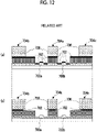
- the base layer 702 at a second stage of working electrodes 704a, 704b, and 704c is excessively etched (so-called over-etched) in a wide range, for example, up to a conductive layer 706 above the base layer 702, so a situation may occur in which overhanging of the conductive layer 706 occurs ((b) of FIG. 12 ).
- an optical waveguide device having an electrode structure capable of preventing over-etching of a base layer of an electrode and preventing overhanging of a conductive layer above the electrode base layer from occurring.
- an optical waveguide device including: a substrate; an optical waveguide formed on the substrate; and a working electrode that controls a light wave propagating through the optical waveguide, in which the working electrode includes a first base layer made of a first material, a first conductive layer on the first base layer, a second base layer made of a second material different from the first material, which is on the first conductive layer, and a second conductive layer on the second base layer, and an edge of the second base layer is covered with the second conductive layer, in a cross-section perpendicular to an extending direction of the optical waveguide.
- the optical waveguide device may further include: a wiring electrode connected to the working electrode, and the wiring electrode may include the second conductive layer extending from the working electrode.
- the second material may be made of titanium (Ti), and the first conductive layer and the second conductive layer may be made of gold (Au).
- the first material may include niobium (Nb).
- a thickness of the first base layer may be equal to or lower than 30 nm, and a thickness of the second base layer may be equal to or higher than 100 nm.
- the optical waveguide may be a protruding optical waveguide including a protruding portion extending on the substrate.
- the two working electrodes sandwiching the optical waveguide in a plane of the substrate may be provided, and a gap of the two working electrodes may be equal to or higher than 0.1 ⁇ m and equal to or lower than 5.0 ⁇ m.
- a conductor pattern including a third base layer made of a third material different from the first material and a third conductive layer on the third base layer may be formed in a region other than a path from an input end to an output end of the optical waveguide, in a region on the substrate.
- the third material may have a light absorption coefficient at a wavelength of light propagating through the optical waveguide, which is larger than a light absorption coefficient of the first material at the wavelength of the light.
- a manufacturing method of the optical waveguide device including: forming a part of the second conductive layer by gold plating.
- an optical modulator including: any of the optical waveguide devices, which is an optical modulation element that modulates light; a case that houses the optical waveguide device; an optical fiber through which light is input to the optical waveguide device; and another optical fiber that guides light output by the optical waveguide device to an outside of the case.
- an optical modulation module including: any of the optical waveguide devices, which is an optical modulation element that modulates light; a case that houses the optical waveguide device; an optical fiber through which light is input to the optical waveguide device; another optical fiber that guides light output by the optical waveguide device to an outside of the case; and a drive circuit that drives the optical waveguide device.
- an optical transmission apparatus including: the optical modulator or the optical modulation module; and an electronic circuit that generates an electrical signal for causing the optical waveguide device to perform a modulation operation.
- an optical waveguide device capable of preventing over-etching of a base layer of a working electrode and preventing overhanging of a conductive layer above the electrode base layer from occurring.
- FIG. 1 is a diagram illustrating a configuration of an optical modulation element 100, which is an optical waveguide device according to a first embodiment of the present invention.
- the optical modulation element 100 uses, for example, a wavelength in a near-infrared wavelength range including a 1.3 ⁇ m bandwidth and/or a 1.55 ⁇ m bandwidth generally used for optical communication as an operating optical wavelength.
- the optical modulation element 100 includes an optical waveguide 104 formed on a substrate 102.
- the substrate 102 is, for example, a thinned X-cut LN substrate having an electro-optic effect, which is processed to a thickness of 20 ⁇ m or lower (for example, 2 ⁇ m).
- the optical waveguide 104 is a protruding optical waveguide (for example, a rib-type optical waveguide or a ridge optical waveguide ) including a band-shaped extending protruding portion formed on a surface of the thinned substrate 102.
- the substrate 102 is, for example, rectangular and has two left and right sides 140a and 140b extending in a vertical direction and facing each other, and upper and lower sides 140c and 140d extending in a lateral direction and facing each other.
- the optical modulation element 100 constitutes a DP-QPSK optical modulator with two nest-shaped Mach-Zehnder type optical waveguides 108a and 108b.
- the nest-shaped Mach-Zehnder type optical waveguide 108a includes two Mach-Zehnder type optical waveguides 110a and 110b.
- the nest-shaped Mach-Zehnder type optical waveguide 108b includes two Mach-Zehnder type optical waveguides 110c and 110d.
- the Mach-Zehnder type optical waveguides 110a and 110b respectively have two parallel waveguides 112a and 112b, and two parallel waveguides 112c and 112d. Further, the Mach-Zehnder type optical waveguides 110c and 110d respectively have two parallel waveguides 112e and 112f, and two parallel waveguides 112g and 112h.
- the input light (an arrow pointing to the right side) input to an input waveguide 106 of the optical waveguide 104 on the lower side of the left side 140a of the substrate 102 is folded back by 180 degrees in a light propagation direction and is branched into two light beams, and the light beams are QPSK-modulated by two nest-shaped Mach-Zehnder type optical waveguides 108a and 108b, respectively.
- the two QPSK-modulated light beams are output from the upper side of the left side 140a of the substrate 102 via output waveguides 126a and 126b, respectively (two arrows pointing to the left side).
- These two output light beams are output from the substrate 102, polarized and combined, for example, by a polarization beam combiner into one optical beam, and transmitted to a transmission optical fiber as a DP-QPSK-modulated optical signal.
- signal electrodes 114-1a and 114-1b to which high-frequency electrical signals for modulation are input are disposed between the two parallel waveguides 112a and 112b of the Mach-Zehnder type optical waveguide 110a and between the two parallel waveguides 112c and 112d of the Mach-Zehnder type optical waveguide 110b, respectively.
- signal electrodes 114-1c and 114-1d into which high-frequency electrical signals for modulation are input are disposed between the two parallel waveguides 112e and 112f of the Mach-Zehnder type optical waveguide 110c, and between the two parallel waveguides 112g and 112h of the Mach-Zehnder type optical waveguide 110d, respectively.
- the signal electrode 114-1a constitutes a coplanar type transmission line together with the ground electrodes 114-2a and 114-2b facing each other across the parallel waveguides 112a and 112b, respectively, and the signal electrode 114-1b constitutes a coplanar type transmission line together with the ground electrodes 114-2b and 114-2c facing each other across the parallel waveguides 112c and 112d, respectively.
- the signal electrode 114-1c constitutes a coplanar type transmission line together with the ground electrodes 114-2c and 114-2d facing each other across the parallel waveguides 112e and 112f, respectively, and the signal electrode 114-1d constitutes a coplanar type transmission line together with the ground electrodes 114-2d and 114-2e facing each other across the parallel waveguides 112e and 112f, respectively.
- nest-shaped Mach-Zehnder type optical waveguides 108a and 108b are collectively referred to as nest-shaped Mach-Zehnder type optical waveguides 108.
- Mach-Zehnder type optical waveguides 110a, 110b, 110c, 110d, 110e, 110f, 110g, and 110h are collectively referred to as Mach-Zehnder type optical waveguides 110.
- parallel waveguides 112a, 112b, 112c, 112d, 112e, 112f, 112g, and 112h are collectively referred to as parallel waveguides 112.
- the signal electrodes 114-1a, 114-1b, 114-1c, and 114-1d are collectively referred to as signal electrodes 114-1.
- the ground electrodes 114-2a, 114-2b, 114-2c, 114-2d, and 114-2e are collectively referred to as ground electrodes 114-2.
- the signal electrode 114-1 and the ground electrode 114-2 are collectively referred to as working electrodes 114.
- the signal electrode 114-1 and the ground electrode 114-2 which are the working electrodes 114, control the light wave propagating in the optical waveguide 104.
- the signal electrode 114-1 and the ground electrode 114-2 are two working electrodes 114 that sandwich the parallel waveguide 112 of the optical waveguide 104 in the plane of the substrate 102.
- the right edges of the signal electrodes 114-1a, 114-1b, 114-1c, and 114-1d are connected to signal wiring electrodes 118-1a, 118-1b, 118-1c, and 118-1d, respectively. Further, the left edges of the signal electrodes 114-1a, 114-1b, 114-1c, and 114-1d are connected to signal wiring electrodes 118-1e, 118-1f, 118-1g, and 118-1h, respectively.
- ground electrodes 114-2a, 114-2b, 114-2c, 114-2d, and 114-2e are connected to ground wiring electrodes 118-2a, 118-2b, 118-2c, 118-2d, and 118-2e, respectively.
- the signal wiring electrodes 118-1a, 118-1b, 118-1c, and 118-1d and the ground wiring electrodes 118-2a, 118-2b, 118-2c, 118-2d, and 118-2e adjacent to these signal wiring electrodes constitute a coplanar type transmission line.
- the left ends of the ground electrodes 114-2a, 114-2b, 114-2c, 114-2d, and 114-2e are connected to ground wiring electrodes 118-2f, 118-2g, 118-2h, 118-2i, and 118-2j, respectively.
- the signal wiring electrodes 118-1e, 118-1f, 118-1g, and 118-1h and the ground wiring electrodes 118-2f, 118-2g, 118-2h, 118-2i, and 118-2j adjacent to the signal wiring electrodes constitute a coplanar type transmission line.
- the signal wiring electrodes 118-1e, 118-1f, 118-1g, and 118-1h extending to the lower side 140d of the substrate 102 are terminated by a termination resistor having a predetermined impedance outside the substrate 102.
- the high-frequency electrical signal input from the signal wiring electrodes 118-1a, 118-1b, 118-1c, and 118-1d extending to the upper side 140c of the substrate 102 becomes a traveling wave to propagate through the signal electrodes 114-1a, 114-1b, 114-1c, and 114-1d, and modulates the light wave propagating through the Mach-Zehnder type optical waveguides 110a, 110b, 110c, and 110d, respectively.
- the signal wiring electrodes 118-1a, 118-1b, 118-1c, 118-1d, 118-1e, 118-1f, 118-1g, and 118-1h are collectively referred to as signal wiring electrodes 118-1.
- the ground wiring electrodes 118-2a, 118-2b, 118-2c, 118-2d, 118-2e, 118-2f, 118-2g, 118-2h, 118-2i, and 118-2j are collectively referred to as ground wiring electrodes 118-2.
- the signal wiring electrode 118-1 and the ground wiring electrode 118-2 are collectively referred to as wiring electrodes 118. That is, the signal wiring electrode 118-1 and the ground wiring electrode 118-2 are the wiring electrodes 118 connected to the working electrode 114.
- a bias electrode 132a that adjusts bias points of the Mach-Zehnder type optical waveguides 110a and 110b, a bias electrode 132b that adjusts bias points of the Mach-Zehnder type optical waveguides 110c and 110d, and a bias electrode 132c that adjusts bias points of the nest-shaped Mach-Zehnder type optical waveguides 108a and 108b are provided, on the substrate 102.
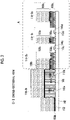
- FIG. 2 is a cross-sectional view taken along line II-II of the optical modulation element 100 illustrated in FIG. 1 .
- FIG. 3 is a cross-sectional view taken along line III-III of the optical modulation element 100 illustrated in FIG. 1 .
- a back surface (lower surface in FIG. 2 ) of the substrate 102 is supported and reinforced by a supporting plate 142.
- the supporting plate 142 is, for example, glass.
- the parallel waveguides 112a, 112b, 112c, and 112d are formed on an upper surface of the substrate 102, as protruding optical waveguides, by protruding portions 144a, 144b, 144c, and 144d formed on the substrate 102, respectively.
- protruding portions 144 are collectively referred to as protruding portions 144.
- the signal electrodes 114-1b and the ground electrodes 114-2b and 114-2c which are the working electrodes 114, are arranged at positions to sandwich the parallel waveguides 112c and 112d in the plane of the substrate 102.
- the signal electrode 114-1b, and the ground electrodes 114-2b and 114-2c are second-stage electrodes including first-stage electrodes 150a, 150b, and 150c, and second-stage electrodes 152a, 152b, and 152c, respectively.
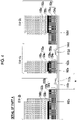
- FIG. 4 is a partial detailed view of part A illustrated in FIG. 2 .
- the signal electrode 114-1b includes a first base layer 154a, a first conductive layer 156a on the first base layer 154a, a second base layer 158a on the first conductive layer 156a, and a second conductive layer 160a on the second base layer 158a.
- the first base layer 154a and the first conductive layer 156a constitute the first-stage electrode 150a
- the second base layer 158a and the second conductive layer 160a constitute the second-stage electrode 152a.
- the first base layer 154a is made of a first material
- the second base layer 158a is made of a second material different from the first material.
- the first material is niobium (Nb) and the second material is titanium (Ti).
- both the first conductive layer 156 and the second conductive layer 160 are gold (Au).
- an edge 162a of the second base layer 158a on the parallel waveguide 112c side is covered with the second conductive layer 160a.
- an edge 162b of the second base layer 158a on the parallel waveguide 112d side is covered with the second conductive layer 160a.
- the ground electrode 114-2b includes a first base layer 154b, a first conductive layer 156b on the first base layer 154b, a second base layer 158b on the first conductive layer 156b, and a second conductive layer 160b on the second base layer 158b.
- the first base layer 154b and the first conductive layer 156b constitute the first-stage electrode 150b
- the second base layer 158b and the second conductive layer 160b constitute the second-stage electrode 152b.
- the first base layer 154b is made of a first material
- the second base layer 158b is made of a second material different from the first material. Then, in the cross-section perpendicular to the extending direction of the parallel waveguide 112, an edge 162c of the second base layer 158b on the parallel waveguide 112c side is covered with the second conductive layer 160b.
- the ground electrode 114-2c includes a first base layer 154c, a first conductive layer 156c on the first base layer 154c, a second base layer 158c on the first conductive layer 156c, and a second conductive layer 160c on the second base layer 158c.
- the first base layer 154c and the first conductive layer 156c constitute the first-stage electrode 150c
- the second base layer 158c and the second conductive layer 160c constitute the second-stage electrode 152c.
- the first base layer 154c is made of a first material
- the second base layer 158c is made of a second material different from the first material. Then, in the cross-section perpendicular to the extending direction of the parallel waveguide 112, an edge 162d of the second base layer 158c on the parallel waveguide 112d side is covered with the second conductive layer 160c.
- the other signal electrodes 114-1a, 114-1c, and 114-1d other than the signal electrode 114-1b, and the other ground electrodes 114-2a, 114-2d, and 114-2e other than the ground electrodes 114-2b and 114-2c are also configured in the same manner as the signal electrodes 114-1a and the ground electrodes 114-2a and 114-2b described above.
- the first base layers, the first conductive layers, the second base layers, and the second conductive layers of the signal electrode 114-1 and the ground electrode 114-2 are collectively referred to as first base layers 154, first conductive layers 156, second base layers 158, and second conductive layers 160, respectively.
- first-stage electrodes including the first base layer 154 and the first conductive layer 156 of the working electrode 114 including the first-stage electrodes 150a, 150b, and 150c illustrated in FIG. 4 , are collectively referred to as first-stage electrodes 150.
- second-stage electrodes including the second base layer 158 and the second conductive layer 160 of the working electrode 114, including the second-stage electrodes 152a, 152b, and 152c are collectively referred to as second-stage electrodes 152.
- edges of the second base layer 158 on the adjacent parallel waveguide 112 side including the edges 162a, 162b, 162c, and 162d are collectively referred to as edges 162.
- the signal electrode 114-1 and the ground electrode 114-2 which are the working electrodes 114, include the first base layer 154 made of a first material, the first conductive layer 156 on the first base layer 154, the second base layer 158, which is the second base layer 158 on the first conductive layer 156c and is made of a second material different from the first material, and the second conductive layer 160 on the second base layer 158, respectively. Then, in the cross-section perpendicular to the extending direction of the parallel waveguide 112, the edge 162 of the second base layer 158 of the working electrode 114 on the parallel waveguide 112 side is covered with the second conductive layer 160.
- the ground wiring electrode 118-2b connected to the ground electrode 114-2b is provided, on the substrate 102.
- the ground wiring electrode 118-2b is configured such that the second-stage electrode 152b of the ground electrode 114-2b is extended on the substrate 102 in a left direction. That is, the ground wiring electrode 118-2b includes the second conductive layer 160b extending from the ground electrode 114-2b.
- a resin layer 146 is provided between the ground wiring electrode 118-2b and the parallel waveguides 112a and 112b.
- the signal wiring electrode 118-1b connected to the signal electrode 114-1b is provided, on the substrate 102.
- the signal wiring electrode 118-1b is configured such that the second-stage electrode 152a of the signal electrode 114-1b is extended on the substrate 102 in the left direction. That is, the signal wiring electrode 118-1b includes the second conductive layer 160 extending from the signal electrode 114-1b.
- the resin layer 146 is provided between the signal wiring electrode 118-1b and the parallel waveguides 112a, 112b, and 112c.
- ground wiring electrodes 118-2 other than the ground wiring electrode 118-2b are also configured in the same manner as the ground wiring electrode 118-2b in FIG. 2 .
- the other signal wiring electrodes 118-1 other than the signal wiring electrodes 118-1b are also configured in the same manner as the signal wiring electrodes 118-1b.
- the optical modulation element 100 includes the wiring electrode 118 connected to the working electrode 114, and the wiring electrode 118 includes the second conductive layer 160 extending from the working electrode 114. Then, the resin layer 146 is formed between the wiring electrode 118 and the optical waveguide 104 under the wiring electrode 118.
- the first material constituting the first base layer 154 of the signal electrode 114-1 and the ground electrode 114-2, which are the working electrodes 114 includes a material different from the second material constituting the second base layer 158, for example, niobium.
- Niobium has a small light absorption coefficient at an operating optical wavelength of the optical modulation element 100 (for example, 1.3 ⁇ m bandwidth and/or 1.55 ⁇ m bandwidth, which are wavelengths for optical communication), as compared with titanium, which is generally used as a base layer material for electrodes in the related art. Therefore, the first-stage electrode 150 of these working electrodes 114 can be disposed closer to the parallel waveguide 112 as compared with the related art.
- a gap W (see FIG. 4 ) between the signal electrode 114-1 and the ground electrode 114-2, which are the two working electrodes 114 sandwiching the parallel waveguide 112, is equal to or higher than 1.0 ⁇ m and equal to or lower than 5.0 ⁇ m.
- the optical modulation element 100 as the second material of the second base layer 158, a material different from the first material, for example, titanium in the same manner as the related art can be used, so that the second-stage electrode 152 can be firmly fixed to the first-stage electrode 150.
- the optical modulation element 100 can achieve a high-frequency optical modulation operation having a lower drive voltage with high reliability, as compared with the related art.
- the edge 162 of the second base layer 158 on the parallel waveguide 112 side, of the signal electrode 114-1 and the ground electrode 114-2, which are the working electrodes 114 is covered with the second conductive layer 160 on the second base layer 158.
- the optical modulation element 100 when a film of the second material (material of the second base layer 158) remaining on the substrate 102 after formation of the second conductive layer 160 of the working electrode 114 is etched, it is possible to prevent the second base layer 158 below the second conductive layer 160 from being over-etched.
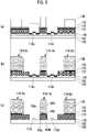
- FIG. 5 is a diagram illustrating an example of an electrode forming step of the optical modulation element 100 in part A in FIG. 2 .
- (a) of FIG. 5 illustrates a state in which a first layer 170 made of a first material and a second layer 172 made of Au are formed on the substrate 102 to perform first patterning, and then a third layer 176 made of a second material and a fourth layer 178 which is an Au thin film are formed.
- the Au thin film of the fourth layer 178 is formed by, for example, electron beam deposition.
- each of the other layers illustrated by the same type of hatching as each of the first layer 170, the second layer 172, the third layer 176, and the fourth layer 178 illustrated on the right side, and a resist 180 and a fifth layer 182 which will be described below, are also the first layer 170, the second layer 172, the third layer 176, the fourth layer 178, the resist 180, and the fifth layer 182.
- the first layer 170 and the second layer 172 are removed above the parallel waveguides 112c and 112d, by the first patterning. Therefore, the third layer 176 and the fourth layer 178 are formed above and around the parallel waveguides 112c and 112d.
- the resist 180 for etching the third layer 176 and the fourth layer 178 is further formed on the fourth layer 178.
- FIG. 5 illustrates a state in which the third layer 176 and the fourth layer 178 formed on the second layer 172 in the state illustrated in (a) of FIG. 5 are etched, and then the fifth layer 182 which is an Au thick film is formed and patterned on the fourth layer 178 by plating.
- the second conductive layer 160 of the signal electrode 114-1b includes the fourth layer 178 and the fifth layer 182, both of which include Au.
- the manufacturing method (manufacturing step) of the optical modulation element 100 includes a step of forming a part of the second conductive layer by gold plating.
- the third layer 176 and the fourth layer 178 located above and around the parallel waveguides 112c and 112d are left so as to reduce potential unevenness on an upper surface of the substrate 102 and ensure homogeneity of the Au thick film when the Au thick film of the fifth layer 182 is formed by plating.
- FIG. 5 illustrates a state in which the third layer 176 and the fourth layer 178 located above and around the parallel waveguides 112c and 112d are removed by etching.
- the edges 162a and 162b of the second base layer 158 of the signal electrode 114-1b on respective sides of the parallel waveguides 112c and 112d are covered with the second conductive layer 160 on the second base layer 158, so that over-etching of the second base layer 158 does not occur. Therefore, the second-stage electrode 152a having an appropriate side surface without overhanging can be formed.
- the ground electrodes 114-2c and 114-2d are the same applies.
- the first base layer 154 constituting the first-stage electrode 150 of the signal electrode 114-1 includes niobium (Nb).
- Niobium has a smaller light absorption coefficient in a near-infrared wavelength range including in the operating optical wavelength of the optical modulation element 100, as compared with titanium (Ti) generally used as a material for the first base layer 154 in the related art. Therefore, in the optical modulation element 100, the working electrode 114 can be provided closer to the parallel waveguide 112, as compared with the related art. Therefore, in the optical modulation element 100, it is possible to increase electric field efficiency and achieve high-frequency and low-voltage operation.
- the material constituting the first base layer 154 may be any material having a smaller light absorption coefficient at the operating optical wavelength as compared with titanium used in the related art, and is not limited to niobium (Nb).
- FIG. 6 is a simulation result of the amount of increase in light absorption loss in the parallel waveguide 112c with respect to a thickness of the first base layer 154 in a case where the first base layer 154 includes various metals.
- the first base layer 154 is not used for the first-stage electrode 150 (in a case of Au single film (only the first conductive layer 156)
- a calculation result in a case where Ti, aluminum (Al), and Nb are used as materials for the first base layer 154 is illustrated.
- a horizontal axis is the thickness t of the first base layer 154
- a vertical axis is the amount of light absorption loss per unit length (1 cm) of the parallel waveguide 112 adjacent to the first base layer 154.
- Au is used as the first conductive layer 156
- 1.55 ⁇ m is set as an operating optical wavelength.
- the amount of light absorption at the operating wavelength of 1.55 ⁇ m of each metal obtained from a light absorption spectra of Ti, Al, and Nb is used.
- a light absorption loss ⁇ 0 in a case of the Au single film illustrated in line 200 (without a base layer) is a light absorption loss as a background in the above-described configuration, and the light absorption loss in the first base layer 154 can be evaluated as the increase in light absorption loss from this reference line.
- Lines 202, 204, and 206 illustrate light absorption losses in a case where a metal constituting the first base layer 154 includes Ti, Al, and Nb, respectively. Among these metals, Ti illustrated by line 202 has the largest light absorption loss, and the light absorption loss increases greatly with a film thickness.
- the thickness of the first base layer 154 including Nb is equal to or lower than 30 nm. If the thickness of the base layer of Nb is within this range, the light absorption loss can be suppressed to a value equal to or lower than 2 ⁇ 0, which is twice the value of ⁇ 0 in the Au single film, or a value of 1/3 or lower of a value in the case of the first base layer 154 using Ti in the related art, which is approximately 6 ⁇ 0.
- FIG. 9 is a diagram illustrating a configuration of an optical modulator 400 according to the second embodiment.
- the optical modulator 400 includes a case 402, the optical modulation element 100 housed in the case 402, and a relay substrate 406. Finally, a cover (not illustrated), which is a plate body, is fixed to an opening portion of the case 402, and the inside of the case 402 is hermetically sealed.
- the optical modulator 400 has signal pins 408 for inputting a high-frequency electrical signal to be used for modulation of the optical modulation element 100, and signal pins 410 for inputting an electrical signal to be used for adjusting an operating point of the optical modulation element 100.
- the optical modulator 400 has an input optical fiber 414 for inputting light into the case 402 and an output optical fiber 420 for guiding the light modulated by the optical modulation element 100 to the outside of the case 402, on the same surface of the case 402 (in the present embodiment, the surface on the left side).
- the input optical fiber 414 and the output optical fiber 420 are respectively fixed to the case 402 via supports 422 and 424 which are fixing members.
- the light input from the input optical fiber 414 is collimated by a lens 430 disposed in the support 422, and then input to the optical modulation element 100 via a lens 434.
- this is only an example, and the light may be input to the optical modulation element 100, based on the related art, for example, by introducing the input optical fiber 414 into the case 402 via the support 422, and connecting an end surface of the introduced input optical fiber 414 to an end surface of the substrate 102 of the optical modulation element 100.
- the light output from the optical modulation element 100 is coupled to the output optical fiber 420 via the optical unit 416 and a lens 418 disposed on the support 424.
- the optical unit 416 may include a polarization beam combiner that combines two modulated light beams output from the optical modulation element 100 into a single beam.
- the relay substrate 406 relays the high-frequency electrical signal input from the signal pins 408 and the electrical signal for adjusting an operating point (bias point) input from the signal pins 410 to the optical modulation element 100, according to a conductor pattern (not illustrated) formed on the relay substrate 406.
- the conductor patterns on the relay substrate 406 are respectively connected to solder configuring one end of the wiring electrode 118 of the optical modulation element 100 by, for example, wire bonding or the like.
- the optical modulator 400 includes a terminator 412 having a predetermined impedance in the case 402.
- the optical modulator 400 having the above-described configuration is configured by using the optical modulation element 100 according to the first embodiment described above, it is possible to achieve a high-frequency optical modulation operation driven at a lower voltage with high reliability, as compared with the related art.
- FIG. 10 is a diagram illustrating a configuration of the optical modulation module 500 according to the present embodiment.
- FIG. 10 for the same components as in the optical modulator 400 according to the second embodiment illustrated in FIG. 9 , the same reference numerals as those illustrated in FIG. 9 are used, and the above description for FIG. 9 is incorporated.
- the optical modulation module 500 has the same configuration as the optical modulator 400 illustrated in FIG. 9 , but differs from the optical modulator 400 in that it includes a circuit substrate 506 instead of the relay substrate 406.
- the circuit substrate 506 includes a drive circuit 508.
- the drive circuit 508 generates a high-frequency electrical signal for driving the optical modulation element 100 based on, for example, a modulation signal supplied from the outside via the signal pins 408, and outputs the generated high-frequency electrical signal to the optical modulation element 100.
- the optical modulation module 500 having the above-described configuration is configured by using the optical modulation element 100 according to the first embodiment described above, it is possible to achieve a high-frequency optical modulation operation having a lower drive voltage with high reliability, as compared with the related art.
- the present embodiment is an optical transmission apparatus 600 equipped with the optical modulator 400 according to the second embodiment.
- FIG. 11 is a diagram illustrating a configuration of the optical transmission apparatus 600 according to the present embodiment.
- the optical transmission apparatus 600 includes the optical modulator 400, a light source 604 that inputs light to the optical modulator 400, a modulator drive unit 606, and a modulation signal generation part 608.
- the above-described optical modulation module 500 can also be used instead of the optical modulator 400 and the modulator drive unit 606.
- the modulation signal generation part 608 is an electronic circuit that generates an electrical signal for causing the optical modulator 400 to perform a modulation operation, which generates, based on transmission data given from the outside, a modulation signal which is a high-frequency signal for causing the optical modulator 400 to perform an optical modulation operation according to the modulation data, and outputs the modulation signal to the modulator drive unit 606.
- the modulator drive unit 606 amplifies the modulation signal input from the modulation signal generation part 608, and outputs a high-frequency electrical signal for driving a signal electrode of the optical modulation element 100 included in the optical modulator 400.
- the optical modulation module 500 provided with a drive circuit 508 including a circuit corresponding to the modulator drive unit 606 inside the case 402 can also be used.
- the high-frequency electrical signal is input to the signal pins 408 of the optical modulator 400 to drive the optical modulation element 100.
- the light output from the light source 604 is modulated by the optical modulator 400, becomes modulated light, and is output from the optical transmission apparatus 600.
- the optical transmission apparatus 600 having the above-described configuration uses the optical modulation element 100 or the like capable of performing a modulation operation with a small wavelength dependence in a small size, in the same manner as the optical modulator 400 according to the second embodiment and the optical modulation module 500 according to the third embodiment described above, appropriate optical transmission can be performed by achieving a high-frequency optical modulation operation driven at a smaller drive voltage with high reliability, as compared with the related art.
- the present invention is not limited to the configuration of the above-described embodiment and its alternative configuration, and can be implemented in various embodiments without departing from the gist thereof.
- the paths of the wiring electrode 118 and the wiring of the bias electrodes 132a, 132b, and 132c are not limited to the paths illustrated in FIG. 1 .
- the paths of the wiring electrode 118 and the bias electrode wiring on the substrate 102 are any paths as long as the paths do not act on the optical waveguide 104, based on the related art.
- the wiring electrode 118 may be extended linearly from the signal electrode 114-1 so as not to act on the optical waveguide 104.
- the bias electrode wiring may be formed by any path so as to reach the side 140b facing the side 140a on which the input waveguide 106 and the output waveguides 126a and 126b are formed, for example.
- a conductor pattern including a third base layer made of a third material different from a first material and a third conductive layer on the third base layer may be formed, in a region other than a path from an input end to an output end of an optical signal of the optical waveguide 104.
- the input end is an edge of the input waveguide 106 to which light is input
- the output end is edges of the output waveguides 126a and 126b through which the light input from the input end is output.
- the region other than the path from the input end to the output end of the optical signal of the optical waveguide 104 means a region in which unnecessary light that is not used as the optical signal propagates.
- a radiated light beam waveguide added to a Y-branched waveguide, through which unnecessary radiated light propagates, a region on the substrate 102 in which stray light propagates, or the like is the "region other than the path from the input end to the output end" described above.
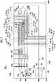
- FIG. 7 illustrates an optical modulation element 100-1, in which a third base layer and a third conductive layer are formed in a region other than a path from an input end to an output end of an optical signal, according to a modification example of the optical modulation element 100 illustrated in FIG. 1 .
- the same reference numerals as those in FIG. 1 are used for the same components as those of the components illustrated in FIG. 1 , and the above description of FIG. 1 is adopted.
- radiated light beam waveguides 130a and 130b for propagating radiated light that leaks without being combined are provided, in a Y-branch coupler 128, which is a Y-branched waveguide constituting the nest-shaped Mach-Zehnder type optical waveguide 108b.
- a conductor pattern 194a is formed in a region, in which the radiated light beam waveguide 130a is formed, on the substrate 102 so as to cover at least a part of the radiated light beam waveguide 130a.
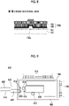
- FIG. 8 is a cross-sectional view taken along line VIII-VIII in FIG. 7 , which is a cross-sectional view of a portion at which the radiated light beam waveguide 130a is formed.
- the conductor pattern 194a covering the radiated light beam waveguide 130a includes a third base layer 190 made of a third material different from the first material described above and a third conductive layer 192 on the third base layer 190.
- the third material can have a light absorption coefficient at a wavelength of light propagating through the optical waveguide 104, which is larger than a light absorption coefficient of the first material at the wavelength of the light.
- the third material is, for example, nickel.
- the unnecessary light propagating through the radiated light beam waveguide 130a is efficiently absorbed by nickel constituting the third base layer 190.
- the above-described niobium can be used as the first material.
- the third material can be titanium.
- conductor patterns 194b and 194c are formed while avoiding the input waveguide 106 so as to overlap a rectangular region 196 illustrated by the dotted rectangle line adjacent to an optical input end of the optical waveguide 104 (a portion of the left side 140a at which the edge of the input waveguide 106 is formed).
- the conductor patterns 194b and 194c include a third base layer and a third conductive layer on the third base layer, in the same manner as the conductor pattern 194a illustrated in FIG. 8 .
- the position of the third base layer formed on the substrate 102 is not limited to the positions of the conductor pattern 194a, 194b, and 194c, and can be any position at which the unnecessary light is absorbed.
- the conductor pattern 194a including the third base layer 190 is formed at one radiated light beam waveguide 130a provided in the Y-branch coupler 128, and the conductor pattern may be formed at the radiated light beam waveguide 130b in the same manner.
- the radiated light beam waveguide may be provided in any other Y-branched portion included in the optical waveguide 104, and the conductor pattern including the third base layer may be formed in each of the radiated light beam waveguides.
- the edge of the radiated light beam waveguide 130a is an output end of an optical signal of the optical waveguide 104, so the conductor pattern including the third base layer is not formed.
- the optical modulation element 100 configured with the substrate 102 which is LN (LiNbO3) is illustrated.
- the optical waveguide device according to the present invention is not limited thereto.
- the optical waveguide device can be an element having any function (optical modulation, optical switch, optical directional coupler, or the like) including a substrate of any material (LN, InP, Si, or the like).
- Such an element can be, for example, a so-called silicon photonics waveguide device.
- the substrate 102 is, for example, an X-cut (substrate normal direction is X-axis of crystal axis) LN substrate (so-called X-plate). Meanwhile, a Z-cut LN substrate can also be used as the substrate 102.
- the optical modulation element 100 which is an optical waveguide device according to the above-described embodiment, has the substrate 102, the optical waveguide 104 formed on the substrate 102, and the working electrode 114 that controls a light wave propagating through the optical waveguide 104 (that is, signal electrode 114-1 and ground electrode 114-2).
- the working electrode 114 includes the first base layer 154 made of a first material (for example, niobium), the first conductive layer 156 on the first base layer 154, the second base layer 158, which is the second base layer 158 on the first conductive layer 156c and is made of a second material (for example, titanium) different from the first material, and the second conductive layer 160 on the second base layer 158.
- the edge of the second base layer 158 on the optical waveguide 104 side for example, the edge 162 on the parallel waveguide 112 side, which is a part of the optical waveguide 104, is covered with the second conductive layer 160.
- the optical modulation element 100 includes the wiring electrode 118 connected to the working electrode 114.
- the wiring electrode 118 includes the second conductive layer 160 extending from the working electrode 114. With this configuration, the wiring electrode 118 can be manufactured at the same time when the second-stage electrode 152 of the working electrode 114 is formed.
- the second material constituting the second base layer 158 is titanium (Ti), and the first conductive layer 156 and the second conductive layer 160 are made of gold (Au).
- Ti titanium
- Au gold
- the second base layer 158, the first conductive layer 156, and the second conductive layer 160 are formed by using titanium and gold used as the material of the base layer and the material of the conductive layer in the related art, respectively. Therefore, these layers can be formed by the same steps in the related art.
- the first material constituting the first base layer 154 is niobium (Nb).
- Nb niobium
- the thickness of the first base layer 154 including niobium is equal to or lower than 30 nm, and a thickness of the second base layer 158 is equal to or higher than 100 nm.
- the second-stage electrode 152 can be firmly fixed on the first-stage electrode 150 by the second base layer 158 having the sufficient thickness while niobium constituting the first base layer 154 suppresses an increase in light absorption loss occurring in the parallel waveguide 112.
- the optical waveguide 104 constituting the optical modulation element 100 is a protruding optical waveguide including the protruding portion 144 extending on the substrate 102.
- the optical modulation element 100 has the two working electrodes 114 (that is, the signal electrode 114-1 and the ground electrode 114-2) sandwiching the parallel waveguide 112 of the optical waveguide 104 in the plane of the substrate 102. Then, the gap between these two working electrodes 114 is equal to or higher than 1.0 ⁇ m and equal to or lower than 5.0 ⁇ m. With this configuration, even in a case where fine unevenness exists on the substrate 102 at a gap of approximately 3 ⁇ m, over-etching of the second base layer 158 of the working electrode 114 can be prevented, and the working electrode 114 having an appropriate side surface shape can be formed.
- the manufacturing step of the optical modulation element 100 includes a step of forming a part of the second conductive layer 160 by gold plating.
- the optical modulator 400 includes the optical modulation element 100 that modulates light, the case 402 that houses the optical modulation element 100, the input optical fiber 414 through which the light is input to the optical modulation element 100, and the output optical fiber 420 that guides the light output from the optical modulation element 100 to the outside of the case 402.
- the optical modulation module 500 includes an optical modulation element 100, a case 402 that houses the optical modulation element 100, an input optical fiber 414 that inputs light to the optical modulation element 100, an output optical fiber 420 that guides the light output by the optical modulation element 100 to the outside of the case 402, and a drive circuit 508 that drives the optical modulation element.
- the optical transmission apparatus 600 includes the optical modulator 400 according to the second embodiment or the optical modulation module 500 according to the third embodiment, and a modulation signal generation part 608 which is an electronic circuit for generating an electrical signal for causing the optical modulation element 100 to perform a modulation operation.
- optical modulator 400 the optical modulation module 500, or the optical transmission apparatus 600 with low power consumption, high-frequency, and low loss.
Landscapes
- Physics & Mathematics (AREA)
- Nonlinear Science (AREA)
- General Physics & Mathematics (AREA)
- Optics & Photonics (AREA)
- Engineering & Computer Science (AREA)
- Electromagnetism (AREA)
- Crystallography & Structural Chemistry (AREA)
- Chemical & Material Sciences (AREA)
- Ceramic Engineering (AREA)
- Microelectronics & Electronic Packaging (AREA)
- Computer Networks & Wireless Communication (AREA)
- Signal Processing (AREA)
- Optical Modulation, Optical Deflection, Nonlinear Optics, Optical Demodulation, Optical Logic Elements (AREA)
Abstract
Description
- This application claims the benefit of
Japanese Patent Application No. 2021-089825 filed May 28, 2021 - The present invention relates to an optical waveguide device, a manufacturing method of an optical modulation element, an optical modulator, an optical modulation module, and an optical transmission apparatus.
- In a commercial optical fiber communication system, an optical modulator incorporating an optical modulation element as an optical waveguide device including an optical waveguide formed on a substrate and a working electrode for controlling a light wave by acting an electric field on the optical waveguide is often used. Among the optical modulation elements, an optical modulation element using LiNbO3 (hereinafter, also referred to as LN) having an electro-optic effect for a substrate can achieve high-frequency optical modulation characteristics with less optical loss, so that it is widely used in optical fiber communication systems for high-frequency, large-capacity backbone optical transmission networks and metro networks.
- As one measure for miniaturization, high-frequency, and power saving of such optical modulation elements, an optical modulator in which an LN substrate is thinned to strengthen an interaction between a signal electric field and a waveguide light in the substrate (that is, to increase electric field efficiency), or an optical modulator using a rib-type optical waveguide or a ridge optical waveguide (hereinafter, collectively referred to as a protruding optical waveguide) configured by forming a band-shaped protruding portion on a surface of the LN substrate is also being put into practical use (for example,
Japanese Laid-open Patent Publication No. 2007-264548 WO 2018/031916 ). - Further, for a high-frequency in an operation speed, in the related art, in order to set an impedance of a working electrode within a predetermined range while matching a speed of an electrical signal propagating through the working electrode with a speed of a light wave propagating through an optical waveguide, the working electrode includes two stages on a substrate (see, for example,
Japanese Laid-open Patent Publication No. 1997-185025 - Meanwhile, when the two-stage electrode is brought close to the protruding optical waveguide in this manner, a complicated and fine uneven shape may exist on a substrate in a process of forming the electrode. Therefore, for example, in a case where a metal film formed on the substrate is etched in a patterning step, an etching rate of the metal film may be different in a plane of the substrate due to an uneven distribution of the corrugated structure on the substrate. As a result, as illustrated in
FIG. 12 , for example, when etching an unnecessary base layer 702 (black-painted layer) formed in a fine uneven portion in the vicinity of protrudingoptical waveguides FIG. 12 ), thebase layer 702 at a second stage of workingelectrodes conductive layer 706 above thebase layer 702, so a situation may occur in which overhanging of theconductive layer 706 occurs ((b) ofFIG. 12 ). - From the background described above, it is desired to achieve an optical waveguide device having an electrode structure capable of preventing over-etching of a base layer of an electrode and preventing overhanging of a conductive layer above the electrode base layer from occurring.
- According to one aspect of the present invention, there is provided an optical waveguide device including: a substrate; an optical waveguide formed on the substrate; and a working electrode that controls a light wave propagating through the optical waveguide, in which the working electrode includes a first base layer made of a first material, a first conductive layer on the first base layer, a second base layer made of a second material different from the first material, which is on the first conductive layer, and a second conductive layer on the second base layer, and an edge of the second base layer is covered with the second conductive layer, in a cross-section perpendicular to an extending direction of the optical waveguide.
- According to another aspect of the present invention, the optical waveguide device may further include: a wiring electrode connected to the working electrode, and the wiring electrode may include the second conductive layer extending from the working electrode.
- According to still another aspect of the present invention, the second material may be made of titanium (Ti), and the first conductive layer and the second conductive layer may be made of gold (Au).
- According to still another aspect of the present invention, the first material may include niobium (Nb).
- According to still another aspect of the present invention, a thickness of the first base layer may be equal to or lower than 30 nm, and a thickness of the second base layer may be equal to or higher than 100 nm.
- According to still another aspect of the present invention, the optical waveguide may be a protruding optical waveguide including a protruding portion extending on the substrate.
- According to still another aspect of the present invention, the two working electrodes sandwiching the optical waveguide in a plane of the substrate may be provided, and a gap of the two working electrodes may be equal to or higher than 0.1 µm and equal to or lower than 5.0 µm.
- According to still another aspect of the present invention, a conductor pattern including a third base layer made of a third material different from the first material and a third conductive layer on the third base layer may be formed in a region other than a path from an input end to an output end of the optical waveguide, in a region on the substrate.
- According to still another aspect of the present invention, the third material may have a light absorption coefficient at a wavelength of light propagating through the optical waveguide, which is larger than a light absorption coefficient of the first material at the wavelength of the light.
- According to still another aspect of the present invention, there is provided a manufacturing method of the optical waveguide device, the method including: forming a part of the second conductive layer by gold plating.
- According to still another aspect of the present invention, there is provided an optical modulator including: any of the optical waveguide devices, which is an optical modulation element that modulates light; a case that houses the optical waveguide device; an optical fiber through which light is input to the optical waveguide device; and another optical fiber that guides light output by the optical waveguide device to an outside of the case.
- According to still another aspect of the present invention, there is provided an optical modulation module including: any of the optical waveguide devices, which is an optical modulation element that modulates light; a case that houses the optical waveguide device; an optical fiber through which light is input to the optical waveguide device; another optical fiber that guides light output by the optical waveguide device to an outside of the case; and a drive circuit that drives the optical waveguide device.
- According to still another aspect of the present invention, there is provided an optical transmission apparatus including: the optical modulator or the optical modulation module; and an electronic circuit that generates an electrical signal for causing the optical waveguide device to perform a modulation operation.
- According to the present invention, there is provided an optical waveguide device capable of preventing over-etching of a base layer of a working electrode and preventing overhanging of a conductive layer above the electrode base layer from occurring.
-
-
FIG. 1 is a diagram illustrating a configuration of an optical modulation element according to a first embodiment of the present invention. -
FIG. 2 is a cross-sectional view taken along line II-II of the optical modulation element illustrated inFIG. 1 . -
FIG. 3 is a cross-sectional view taken along line III-III of the optical modulation element illustrated inFIG. 1 . -
FIG. 4 is a partial detailed view of part A illustrated inFIG. 2 . -
FIG. 5 is a diagram describing an electrode forming step in part B illustrated inFIG. 2 . -
FIG. 6 is a simulation result of the amount of increase in light absorption loss with respect to a thickness of a first base layer in a case where various metals are used as the first base layer. -
FIG. 7 is a diagram illustrating a configuration of an optical modulation element according to a modification example of a first embodiment. -
FIG. 8 is a cross-sectional view taken along line VIII-VIII of the optical modulation element illustrated inFIG. 7 . -
FIG. 9 is a diagram illustrating a configuration of an optical modulator according to a second embodiment of the present invention. -
FIG. 10 is a diagram illustrating a configuration of an optical modulation module according to a third embodiment of the present invention. -
FIG. 11 is a diagram illustrating a configuration of an optical transmission apparatus according to a fourth embodiment of the present invention. -
FIG. 12 is a diagram describing electrode formation of an optical waveguide device in the related art. - Hereinafter, embodiments of the present invention will be described with reference to the drawings.
-
FIG. 1 is a diagram illustrating a configuration of anoptical modulation element 100, which is an optical waveguide device according to a first embodiment of the present invention. Theoptical modulation element 100 uses, for example, a wavelength in a near-infrared wavelength range including a 1.3 µm bandwidth and/or a 1.55 µm bandwidth generally used for optical communication as an operating optical wavelength. - The
optical modulation element 100 includes anoptical waveguide 104 formed on asubstrate 102. Thesubstrate 102 is, for example, a thinned X-cut LN substrate having an electro-optic effect, which is processed to a thickness of 20 µm or lower (for example, 2 µm). Theoptical waveguide 104 is a protruding optical waveguide (for example, a rib-type optical waveguide or a ridge optical waveguide ) including a band-shaped extending protruding portion formed on a surface of thethinned substrate 102. - The
substrate 102 is, for example, rectangular and has two left andright sides lower sides - The
optical modulation element 100 constitutes a DP-QPSK optical modulator with two nest-shaped Mach-Zehnder typeoptical waveguides optical waveguide 108a includes two Mach-Zehnder typeoptical waveguides optical waveguide 108b includes two Mach-Zehnder typeoptical waveguides - The Mach-Zehnder type
optical waveguides parallel waveguides parallel waveguides optical waveguides parallel waveguides parallel waveguides - The input light (an arrow pointing to the right side) input to an
input waveguide 106 of theoptical waveguide 104 on the lower side of theleft side 140a of thesubstrate 102 is folded back by 180 degrees in a light propagation direction and is branched into two light beams, and the light beams are QPSK-modulated by two nest-shaped Mach-Zehnder typeoptical waveguides left side 140a of thesubstrate 102 viaoutput waveguides - These two output light beams are output from the
substrate 102, polarized and combined, for example, by a polarization beam combiner into one optical beam, and transmitted to a transmission optical fiber as a DP-QPSK-modulated optical signal. - For QPSK modulation in the nest-shaped Mach-Zehnder type
optical waveguide 108a, signal electrodes 114-1a and 114-1b to which high-frequency electrical signals for modulation are input are disposed between the twoparallel waveguides optical waveguide 110a and between the twoparallel waveguides optical waveguide 110b, respectively. - Further, for QPSK modulation in the nest-shaped Mach-Zehnder type
optical waveguide 108b, signal electrodes 114-1c and 114-1d into which high-frequency electrical signals for modulation are input are disposed between the twoparallel waveguides optical waveguide 110c, and between the twoparallel waveguides optical waveguide 110d, respectively. - The signal electrode 114-1a constitutes a coplanar type transmission line together with the ground electrodes 114-2a and 114-2b facing each other across the
parallel waveguides parallel waveguides - The signal electrode 114-1c constitutes a coplanar type transmission line together with the ground electrodes 114-2c and 114-2d facing each other across the
parallel waveguides parallel waveguides - Hereinafter, the nest-shaped Mach-Zehnder type
optical waveguides optical waveguides parallel waveguides - Further, the signal electrode 114-1 and the ground electrode 114-2 are collectively referred to as working electrodes 114. The signal electrode 114-1 and the ground electrode 114-2, which are the working electrodes 114, control the light wave propagating in the
optical waveguide 104. Further, the signal electrode 114-1 and the ground electrode 114-2 are two working electrodes 114 that sandwich the parallel waveguide 112 of theoptical waveguide 104 in the plane of thesubstrate 102. - The right edges of the signal electrodes 114-1a, 114-1b, 114-1c, and 114-1d are connected to signal wiring electrodes 118-1a, 118-1b, 118-1c, and 118-1d, respectively. Further, the left edges of the signal electrodes 114-1a, 114-1b, 114-1c, and 114-1d are connected to signal wiring electrodes 118-1e, 118-1f, 118-1g, and 118-1h, respectively.
- The right ends of the ground electrodes 114-2a, 114-2b, 114-2c, 114-2d, and 114-2e are connected to ground wiring electrodes 118-2a, 118-2b, 118-2c, 118-2d, and 118-2e, respectively. Thus, the signal wiring electrodes 118-1a, 118-1b, 118-1c, and 118-1d and the ground wiring electrodes 118-2a, 118-2b, 118-2c, 118-2d, and 118-2e adjacent to these signal wiring electrodes constitute a coplanar type transmission line.
- In the same manner, the left ends of the ground electrodes 114-2a, 114-2b, 114-2c, 114-2d, and 114-2e are connected to ground wiring electrodes 118-2f, 118-2g, 118-2h, 118-2i, and 118-2j, respectively. Thus, the signal wiring electrodes 118-1e, 118-1f, 118-1g, and 118-1h and the ground wiring electrodes 118-2f, 118-2g, 118-2h, 118-2i, and 118-2j adjacent to the signal wiring electrodes constitute a coplanar type transmission line.
- The signal wiring electrodes 118-1e, 118-1f, 118-1g, and 118-1h extending to the
lower side 140d of thesubstrate 102 are terminated by a termination resistor having a predetermined impedance outside thesubstrate 102. - Thus, the high-frequency electrical signal input from the signal wiring electrodes 118-1a, 118-1b, 118-1c, and 118-1d extending to the
upper side 140c of thesubstrate 102 becomes a traveling wave to propagate through the signal electrodes 114-1a, 114-1b, 114-1c, and 114-1d, and modulates the light wave propagating through the Mach-Zehnder typeoptical waveguides - Hereinafter, the signal wiring electrodes 118-1a, 118-1b, 118-1c, 118-1d, 118-1e, 118-1f, 118-1g, and 118-1h are collectively referred to as signal wiring electrodes 118-1. Further, the ground wiring electrodes 118-2a, 118-2b, 118-2c, 118-2d, 118-2e, 118-2f, 118-2g, 118-2h, 118-2i, and 118-2j are collectively referred to as ground wiring electrodes 118-2. Further, the signal wiring electrode 118-1 and the ground wiring electrode 118-2 are collectively referred to as wiring electrodes 118. That is, the signal wiring electrode 118-1 and the ground wiring electrode 118-2 are the wiring electrodes 118 connected to the working electrode 114.
- Further, a
bias electrode 132a that adjusts bias points of the Mach-Zehnder typeoptical waveguides bias electrode 132b that adjusts bias points of the Mach-Zehnder typeoptical waveguides bias electrode 132c that adjusts bias points of the nest-shaped Mach-Zehnder typeoptical waveguides substrate 102. -
FIG. 2 is a cross-sectional view taken along line II-II of theoptical modulation element 100 illustrated inFIG. 1 . Further,FIG. 3 is a cross-sectional view taken along line III-III of theoptical modulation element 100 illustrated inFIG. 1 . A back surface (lower surface inFIG. 2 ) of thesubstrate 102 is supported and reinforced by a supportingplate 142. The supportingplate 142 is, for example, glass. Theparallel waveguides substrate 102, as protruding optical waveguides, by protrudingportions substrate 102, respectively. The four dotted ellipses schematically illustrate light propagating through theparallel waveguide substrate 102 constituting theoptical waveguide 104, including the protrudingportions - With reference to
FIG. 2 , on thesubstrate 102, the signal electrodes 114-1b and the ground electrodes 114-2b and 114-2c, which are the working electrodes 114, are arranged at positions to sandwich theparallel waveguides substrate 102. The signal electrode 114-1b, and the ground electrodes 114-2b and 114-2c are second-stage electrodes including first-stage electrodes stage electrodes -
FIG. 4 is a partial detailed view of part A illustrated inFIG. 2 . The signal electrode 114-1b includes afirst base layer 154a, a firstconductive layer 156a on thefirst base layer 154a, asecond base layer 158a on the firstconductive layer 156a, and a secondconductive layer 160a on thesecond base layer 158a. Thefirst base layer 154a and the firstconductive layer 156a constitute the first-stage electrode 150a, and thesecond base layer 158a and the secondconductive layer 160a constitute the second-stage electrode 152a. - The
first base layer 154a is made of a first material, and thesecond base layer 158a is made of a second material different from the first material. In the present embodiment, the first material is niobium (Nb) and the second material is titanium (Ti). Further, both the first conductive layer 156 and the secondconductive layer 160 are gold (Au). - Then, in a cross-section perpendicular to an extending direction of the parallel waveguide 112, an
edge 162a of thesecond base layer 158a on theparallel waveguide 112c side is covered with the secondconductive layer 160a. In the same manner, in the cross-section perpendicular to the extending direction of the parallel waveguide 112, anedge 162b of thesecond base layer 158a on theparallel waveguide 112d side is covered with the secondconductive layer 160a. - Further, the ground electrode 114-2b includes a
first base layer 154b, a first conductive layer 156b on thefirst base layer 154b, asecond base layer 158b on the first conductive layer 156b, and a secondconductive layer 160b on thesecond base layer 158b. Thefirst base layer 154b and the first conductive layer 156b constitute the first-stage electrode 150b, and thesecond base layer 158b and the secondconductive layer 160b constitute the second-stage electrode 152b. Thefirst base layer 154b is made of a first material, and thesecond base layer 158b is made of a second material different from the first material. Then, in the cross-section perpendicular to the extending direction of the parallel waveguide 112, anedge 162c of thesecond base layer 158b on theparallel waveguide 112c side is covered with the secondconductive layer 160b. - In the same manner, the ground electrode 114-2c includes a
first base layer 154c, a firstconductive layer 156c on thefirst base layer 154c, asecond base layer 158c on the firstconductive layer 156c, and a secondconductive layer 160c on thesecond base layer 158c. Thefirst base layer 154c and the firstconductive layer 156c constitute the first-stage electrode 150c, and thesecond base layer 158c and the secondconductive layer 160c constitute the second-stage electrode 152c. Thefirst base layer 154c is made of a first material, and thesecond base layer 158c is made of a second material different from the first material. Then, in the cross-section perpendicular to the extending direction of the parallel waveguide 112, anedge 162d of thesecond base layer 158c on theparallel waveguide 112d side is covered with the secondconductive layer 160c. - The other signal electrodes 114-1a, 114-1c, and 114-1d other than the signal electrode 114-1b, and the other ground electrodes 114-2a, 114-2d, and 114-2e other than the ground electrodes 114-2b and 114-2c are also configured in the same manner as the signal electrodes 114-1a and the ground electrodes 114-2a and 114-2b described above. Hereinafter, the first base layers, the first conductive layers, the second base layers, and the second conductive layers of the signal electrode 114-1 and the ground electrode 114-2 are collectively referred to as first base layers 154, first conductive layers 156, second base layers 158, and second
conductive layers 160, respectively. - Further, the first-stage electrodes including the first base layer 154 and the first conductive layer 156 of the working electrode 114, including the first-
stage electrodes FIG. 4 , are collectively referred to as first-stage electrodes 150. Further, the second-stage electrodes including thesecond base layer 158 and the secondconductive layer 160 of the working electrode 114, including the second-stage electrodes second base layer 158 on the adjacent parallel waveguide 112 side, including theedges - That is, in the
optical modulation element 100, the signal electrode 114-1 and the ground electrode 114-2, which are the working electrodes 114, include the first base layer 154 made of a first material, the first conductive layer 156 on the first base layer 154, thesecond base layer 158, which is thesecond base layer 158 on the firstconductive layer 156c and is made of a second material different from the first material, and the secondconductive layer 160 on thesecond base layer 158, respectively. Then, in the cross-section perpendicular to the extending direction of the parallel waveguide 112, the edge 162 of thesecond base layer 158 of the working electrode 114 on the parallel waveguide 112 side is covered with the secondconductive layer 160. - With reference to
FIG. 2 , the ground wiring electrode 118-2b connected to the ground electrode 114-2b is provided, on thesubstrate 102. The ground wiring electrode 118-2b is configured such that the second-stage electrode 152b of the ground electrode 114-2b is extended on thesubstrate 102 in a left direction. That is, the ground wiring electrode 118-2b includes the secondconductive layer 160b extending from the ground electrode 114-2b. In the present embodiment, aresin layer 146 is provided between the ground wiring electrode 118-2b and theparallel waveguides - With reference to
FIG. 3 , the signal wiring electrode 118-1b connected to the signal electrode 114-1b is provided, on thesubstrate 102. In the same manner as the ground wiring electrode 118-2b inFIG. 2 , the signal wiring electrode 118-1b is configured such that the second-stage electrode 152a of the signal electrode 114-1b is extended on thesubstrate 102 in the left direction. That is, the signal wiring electrode 118-1b includes the secondconductive layer 160 extending from the signal electrode 114-1b. In the present embodiment, theresin layer 146 is provided between the signal wiring electrode 118-1b and theparallel waveguides - The other ground wiring electrodes 118-2 other than the ground wiring electrode 118-2b are also configured in the same manner as the ground wiring electrode 118-2b in
FIG. 2 . Further, the other signal wiring electrodes 118-1 other than the signal wiring electrodes 118-1b are also configured in the same manner as the signal wiring electrodes 118-1b. - That is, the
optical modulation element 100 includes the wiring electrode 118 connected to the working electrode 114, and the wiring electrode 118 includes the secondconductive layer 160 extending from the working electrode 114. Then, theresin layer 146 is formed between the wiring electrode 118 and theoptical waveguide 104 under the wiring electrode 118. - In the
optical modulation element 100 having the configuration described above, the first material constituting the first base layer 154 of the signal electrode 114-1 and the ground electrode 114-2, which are the working electrodes 114, includes a material different from the second material constituting thesecond base layer 158, for example, niobium. Niobium has a small light absorption coefficient at an operating optical wavelength of the optical modulation element 100 (for example, 1.3 µm bandwidth and/or 1.55 µm bandwidth, which are wavelengths for optical communication), as compared with titanium, which is generally used as a base layer material for electrodes in the related art. Therefore, the first-stage electrode 150 of these working electrodes 114 can be disposed closer to the parallel waveguide 112 as compared with the related art. For example, in the present embodiment, a gap W (seeFIG. 4 ) between the signal electrode 114-1 and the ground electrode 114-2, which are the two working electrodes 114 sandwiching the parallel waveguide 112, is equal to or higher than 1.0 µm and equal to or lower than 5.0 µm. - On the other hand, in the
optical modulation element 100, as the second material of thesecond base layer 158, a material different from the first material, for example, titanium in the same manner as the related art can be used, so that the second-stage electrode 152 can be firmly fixed to the first-stage electrode 150. As a result, theoptical modulation element 100 can achieve a high-frequency optical modulation operation having a lower drive voltage with high reliability, as compared with the related art. - Further, in particular, in the
optical modulation element 100, as illustrated inFIG. 4 , in the cross-section perpendicular to the extending direction of the parallel waveguide 112, the edge 162 of thesecond base layer 158 on the parallel waveguide 112 side, of the signal electrode 114-1 and the ground electrode 114-2, which are the working electrodes 114, is covered with the secondconductive layer 160 on thesecond base layer 158. Thus, in theoptical modulation element 100, when a film of the second material (material of the second base layer 158) remaining on thesubstrate 102 after formation of the secondconductive layer 160 of the working electrode 114 is etched, it is possible to prevent thesecond base layer 158 below the secondconductive layer 160 from being over-etched. As a result, in theoptical modulation element 100, it is possible to prevent overhanging as illustrated inFIG. 12 from occurring in the secondconductive layer 160 due to the over-etching of thesecond base layer 158. -
FIG. 5 is a diagram illustrating an example of an electrode forming step of theoptical modulation element 100 in part A inFIG. 2 .(a) ofFIG. 5 illustrates a state in which afirst layer 170 made of a first material and asecond layer 172 made of Au are formed on thesubstrate 102 to perform first patterning, and then athird layer 176 made of a second material and afourth layer 178 which is an Au thin film are formed. Here, the Au thin film of thefourth layer 178 is formed by, for example, electron beam deposition. - In each of (a), (b), and (c) of
FIG. 5 , it is understood that each of the other layers illustrated by the same type of hatching as each of thefirst layer 170, thesecond layer 172, thethird layer 176, and thefourth layer 178 illustrated on the right side, and a resist 180 and afifth layer 182 which will be described below, are also thefirst layer 170, thesecond layer 172, thethird layer 176, thefourth layer 178, the resist 180, and thefifth layer 182. - In (a) of
FIG. 5 , thefirst layer 170 and thesecond layer 172 are removed above theparallel waveguides third layer 176 and thefourth layer 178 are formed above and around theparallel waveguides FIG. 5 , the resist 180 for etching thethird layer 176 and thefourth layer 178 is further formed on thefourth layer 178. - (b) of
FIG. 5 illustrates a state in which thethird layer 176 and thefourth layer 178 formed on thesecond layer 172 in the state illustrated in (a) ofFIG. 5 are etched, and then thefifth layer 182 which is an Au thick film is formed and patterned on thefourth layer 178 by plating. The secondconductive layer 160 of the signal electrode 114-1b includes thefourth layer 178 and thefifth layer 182, both of which include Au. The same applies to the ground electrodes 114-2c and 114-2d. That is, the manufacturing method (manufacturing step) of theoptical modulation element 100 includes a step of forming a part of the second conductive layer by gold plating. - In (b) of
FIG. 5 , thethird layer 176 and thefourth layer 178 located above and around theparallel waveguides substrate 102 and ensure homogeneity of the Au thick film when the Au thick film of thefifth layer 182 is formed by plating. - (c) of
FIG. 5 illustrates a state in which thethird layer 176 and thefourth layer 178 located above and around theparallel waveguides edges second base layer 158 of the signal electrode 114-1b on respective sides of theparallel waveguides conductive layer 160 on thesecond base layer 158, so that over-etching of thesecond base layer 158 does not occur. Therefore, the second-stage electrode 152a having an appropriate side surface without overhanging can be formed. The same applies to the ground electrodes 114-2c and 114-2d. - Meanwhile, in the present embodiment, the first base layer 154 constituting the first-stage electrode 150 of the signal electrode 114-1 includes niobium (Nb). Niobium has a smaller light absorption coefficient in a near-infrared wavelength range including in the operating optical wavelength of the
optical modulation element 100, as compared with titanium (Ti) generally used as a material for the first base layer 154 in the related art. Therefore, in theoptical modulation element 100, the working electrode 114 can be provided closer to the parallel waveguide 112, as compared with the related art. Therefore, in theoptical modulation element 100, it is possible to increase electric field efficiency and achieve high-frequency and low-voltage operation. - As described above, the material constituting the first base layer 154 may be any material having a smaller light absorption coefficient at the operating optical wavelength as compared with titanium used in the related art, and is not limited to niobium (Nb).
FIG. 6 is a simulation result of the amount of increase in light absorption loss in theparallel waveguide 112c with respect to a thickness of the first base layer 154 in a case where the first base layer 154 includes various metals. InFIG. 6 , in addition to a case where the first base layer 154 is not used for the first-stage electrode 150 (in a case of Au single film (only the first conductive layer 156)), a calculation result in a case where Ti, aluminum (Al), and Nb are used as materials for the first base layer 154 is illustrated. - In
FIG. 6 , a horizontal axis is the thickness t of the first base layer 154, and a vertical axis is the amount of light absorption loss per unit length (1 cm) of the parallel waveguide 112 adjacent to the first base layer 154. In the simulation, it is assumed that Au is used as the first conductive layer 156, and 1.55 µm is set as an operating optical wavelength. Further, in calculating the light absorption loss, the amount of light absorption at the operating wavelength of 1.55 µm of each metal obtained from a light absorption spectra of Ti, Al, and Nb is used. - A light absorption loss α0 in a case of the Au single film illustrated in line 200 (without a base layer) is a light absorption loss as a background in the above-described configuration, and the light absorption loss in the first base layer 154 can be evaluated as the increase in light absorption loss from this reference line.
-
Lines line 202 has the largest light absorption loss, and the light absorption loss increases greatly with a film thickness. - On the other hand, in
lines FIG. 6 , in a case where the first base layer 154 is Al (line 204), the light absorption loss is the smallest, and the light absorption loss is substantially constant with respect to the thickness of the base layer. Meanwhile, it is generally known that Al has a low adhesion strength to a substrate. - From
lines FIG. 6 , it is desirable that the thickness of the first base layer 154 including Nb is equal to or lower than 30 nm. If the thickness of the base layer of Nb is within this range, the light absorption loss can be suppressed to a value equal to or lower than 2α0, which is twice the value of α0 in the Au single film, or a value of 1/3 or lower of a value in the case of the first base layer 154 using Ti in the related art, which is approximately 6α0. - Next, a second embodiment of the present invention will be described. The present embodiment is an optical modulator using the
optical modulation element 100 according to the first embodiment described above.FIG. 9 is a diagram illustrating a configuration of anoptical modulator 400 according to the second embodiment. Theoptical modulator 400 includes acase 402, theoptical modulation element 100 housed in thecase 402, and arelay substrate 406. Finally, a cover (not illustrated), which is a plate body, is fixed to an opening portion of thecase 402, and the inside of thecase 402 is hermetically sealed. - The
optical modulator 400 has signal pins 408 for inputting a high-frequency electrical signal to be used for modulation of theoptical modulation element 100, and signalpins 410 for inputting an electrical signal to be used for adjusting an operating point of theoptical modulation element 100. - Further, the
optical modulator 400 has an inputoptical fiber 414 for inputting light into thecase 402 and an outputoptical fiber 420 for guiding the light modulated by theoptical modulation element 100 to the outside of thecase 402, on the same surface of the case 402 (in the present embodiment, the surface on the left side). - Here, the input
optical fiber 414 and the outputoptical fiber 420 are respectively fixed to thecase 402 viasupports optical fiber 414 is collimated by alens 430 disposed in thesupport 422, and then input to theoptical modulation element 100 via alens 434. Meanwhile, this is only an example, and the light may be input to theoptical modulation element 100, based on the related art, for example, by introducing the inputoptical fiber 414 into thecase 402 via thesupport 422, and connecting an end surface of the introduced inputoptical fiber 414 to an end surface of thesubstrate 102 of theoptical modulation element 100. - The light output from the
optical modulation element 100 is coupled to the outputoptical fiber 420 via theoptical unit 416 and alens 418 disposed on thesupport 424. Theoptical unit 416 may include a polarization beam combiner that combines two modulated light beams output from theoptical modulation element 100 into a single beam. - The
relay substrate 406 relays the high-frequency electrical signal input from the signal pins 408 and the electrical signal for adjusting an operating point (bias point) input from the signal pins 410 to theoptical modulation element 100, according to a conductor pattern (not illustrated) formed on therelay substrate 406. The conductor patterns on therelay substrate 406 are respectively connected to solder configuring one end of the wiring electrode 118 of theoptical modulation element 100 by, for example, wire bonding or the like. Further, theoptical modulator 400 includes aterminator 412 having a predetermined impedance in thecase 402. - Since the
optical modulator 400 having the above-described configuration is configured by using theoptical modulation element 100 according to the first embodiment described above, it is possible to achieve a high-frequency optical modulation operation driven at a lower voltage with high reliability, as compared with the related art. - Next, a third embodiment of the present invention will be described. The present embodiment is an
optical modulation module 500 using the optical modulation element according to any one of the above-described embodiments or modification examples.FIG. 10 is a diagram illustrating a configuration of theoptical modulation module 500 according to the present embodiment. InFIG. 10 , for the same components as in theoptical modulator 400 according to the second embodiment illustrated inFIG. 9 , the same reference numerals as those illustrated inFIG. 9 are used, and the above description forFIG. 9 is incorporated. - The
optical modulation module 500 has the same configuration as theoptical modulator 400 illustrated inFIG. 9 , but differs from theoptical modulator 400 in that it includes acircuit substrate 506 instead of therelay substrate 406. Thecircuit substrate 506 includes adrive circuit 508. Thedrive circuit 508 generates a high-frequency electrical signal for driving theoptical modulation element 100 based on, for example, a modulation signal supplied from the outside via the signal pins 408, and outputs the generated high-frequency electrical signal to theoptical modulation element 100. - Since the
optical modulation module 500 having the above-described configuration is configured by using theoptical modulation element 100 according to the first embodiment described above, it is possible to achieve a high-frequency optical modulation operation having a lower drive voltage with high reliability, as compared with the related art. - Next, a fourth embodiment of the present invention will be described. The present embodiment is an
optical transmission apparatus 600 equipped with theoptical modulator 400 according to the second embodiment.FIG. 11 is a diagram illustrating a configuration of theoptical transmission apparatus 600 according to the present embodiment. Theoptical transmission apparatus 600 includes theoptical modulator 400, alight source 604 that inputs light to theoptical modulator 400, amodulator drive unit 606, and a modulationsignal generation part 608. The above-describedoptical modulation module 500 can also be used instead of theoptical modulator 400 and themodulator drive unit 606. - The modulation
signal generation part 608 is an electronic circuit that generates an electrical signal for causing theoptical modulator 400 to perform a modulation operation, which generates, based on transmission data given from the outside, a modulation signal which is a high-frequency signal for causing theoptical modulator 400 to perform an optical modulation operation according to the modulation data, and outputs the modulation signal to themodulator drive unit 606. - The
modulator drive unit 606 amplifies the modulation signal input from the modulationsignal generation part 608, and outputs a high-frequency electrical signal for driving a signal electrode of theoptical modulation element 100 included in theoptical modulator 400. As described above, instead of theoptical modulator 400 and themodulator drive unit 606, for example, theoptical modulation module 500 provided with adrive circuit 508 including a circuit corresponding to themodulator drive unit 606 inside thecase 402 can also be used. - The high-frequency electrical signal is input to the signal pins 408 of the
optical modulator 400 to drive theoptical modulation element 100. Thus, the light output from thelight source 604 is modulated by theoptical modulator 400, becomes modulated light, and is output from theoptical transmission apparatus 600. - Since the
optical transmission apparatus 600 having the above-described configuration uses theoptical modulation element 100 or the like capable of performing a modulation operation with a small wavelength dependence in a small size, in the same manner as theoptical modulator 400 according to the second embodiment and theoptical modulation module 500 according to the third embodiment described above, appropriate optical transmission can be performed by achieving a high-frequency optical modulation operation driven at a smaller drive voltage with high reliability, as compared with the related art. - The present invention is not limited to the configuration of the above-described embodiment and its alternative configuration, and can be implemented in various embodiments without departing from the gist thereof.
- For example, in the
optical modulation element 100 illustrated inFIG. 1 , the paths of the wiring electrode 118 and the wiring of thebias electrodes FIG. 1 . The paths of the wiring electrode 118 and the bias electrode wiring on thesubstrate 102 are any paths as long as the paths do not act on theoptical waveguide 104, based on the related art. For example, the wiring electrode 118 may be extended linearly from the signal electrode 114-1 so as not to act on theoptical waveguide 104. Further, the bias electrode wiring may be formed by any path so as to reach theside 140b facing theside 140a on which theinput waveguide 106 and theoutput waveguides - Further, in the region on the
substrate 102, a conductor pattern including a third base layer made of a third material different from a first material and a third conductive layer on the third base layer may be formed, in a region other than a path from an input end to an output end of an optical signal of theoptical waveguide 104. Here, the input end is an edge of theinput waveguide 106 to which light is input, and the output end is edges of theoutput waveguides optical waveguide 104 means a region in which unnecessary light that is not used as the optical signal propagates. For example, a radiated light beam waveguide added to a Y-branched waveguide, through which unnecessary radiated light propagates, a region on thesubstrate 102 in which stray light propagates, or the like is the "region other than the path from the input end to the output end" described above. -
FIG. 7 illustrates an optical modulation element 100-1, in which a third base layer and a third conductive layer are formed in a region other than a path from an input end to an output end of an optical signal, according to a modification example of theoptical modulation element 100 illustrated inFIG. 1 . InFIG. 7 , the same reference numerals as those inFIG. 1 are used for the same components as those of the components illustrated inFIG. 1 , and the above description ofFIG. 1 is adopted. - In the optical modulation element 100-1 illustrated in
FIG. 7 , in addition to the components of theoptical modulation element 100 illustrated inFIG. 1 , radiatedlight beam waveguides branch coupler 128, which is a Y-branched waveguide constituting the nest-shaped Mach-Zehnder typeoptical waveguide 108b. Then, aconductor pattern 194a is formed in a region, in which the radiatedlight beam waveguide 130a is formed, on thesubstrate 102 so as to cover at least a part of the radiatedlight beam waveguide 130a. -
FIG. 8 is a cross-sectional view taken along line VIII-VIII inFIG. 7 , which is a cross-sectional view of a portion at which the radiatedlight beam waveguide 130a is formed. Theconductor pattern 194a covering the radiatedlight beam waveguide 130a includes athird base layer 190 made of a third material different from the first material described above and a thirdconductive layer 192 on thethird base layer 190. - Here, the third material can have a light absorption coefficient at a wavelength of light propagating through the
optical waveguide 104, which is larger than a light absorption coefficient of the first material at the wavelength of the light. The third material is, for example, nickel. Thus, the unnecessary light propagating through the radiatedlight beam waveguide 130a is efficiently absorbed by nickel constituting thethird base layer 190. In this case as well, the above-described niobium can be used as the first material. Further, the third material can be titanium. - In the optical modulation element 100-1 illustrated in
FIG. 7 , on thesubstrate 102,conductor patterns input waveguide 106 so as to overlap arectangular region 196 illustrated by the dotted rectangle line adjacent to an optical input end of the optical waveguide 104 (a portion of theleft side 140a at which the edge of theinput waveguide 106 is formed). Theconductor patterns conductor pattern 194a illustrated inFIG. 8 . Thus, unnecessary light input from the optical input end and propagating on thesubstrate 102 without being coupled to theinput waveguide 106 can be effectively absorbed by theconductor patterns - The position of the third base layer formed on the
substrate 102 is not limited to the positions of theconductor pattern FIG. 7 , theconductor pattern 194a including thethird base layer 190 is formed at one radiatedlight beam waveguide 130a provided in the Y-branch coupler 128, and the conductor pattern may be formed at the radiatedlight beam waveguide 130b in the same manner. Further, the radiated light beam waveguide may be provided in any other Y-branched portion included in theoptical waveguide 104, and the conductor pattern including the third base layer may be formed in each of the radiated light beam waveguides. For example, in a case where a light-receiving element is disposed at an edge of the radiatedlight beam waveguide 130a to monitor the amount of light output from the radiatedlight beam waveguide 130a, the edge of the radiatedlight beam waveguide 130a is an output end of an optical signal of theoptical waveguide 104, so the conductor pattern including the third base layer is not formed. - With these configurations, it is possible to suppress the absorption of the light wave due to the working electrode that controls the light wave, and it is possible to effectively remove the unnecessary light propagating on the
substrate 102. - Further, in the first embodiment, as an example of the optical waveguide device according to the present invention, the
optical modulation element 100 configured with thesubstrate 102 which is LN (LiNbO3) is illustrated. Meanwhile, the optical waveguide device according to the present invention is not limited thereto. The optical waveguide device can be an element having any function (optical modulation, optical switch, optical directional coupler, or the like) including a substrate of any material (LN, InP, Si, or the like). Such an element can be, for example, a so-called silicon photonics waveguide device. - Further, in the above-described embodiment, the
substrate 102 is, for example, an X-cut (substrate normal direction is X-axis of crystal axis) LN substrate (so-called X-plate). Meanwhile, a Z-cut LN substrate can also be used as thesubstrate 102. - As described above, the
optical modulation element 100, which is an optical waveguide device according to the above-described embodiment, has thesubstrate 102, theoptical waveguide 104 formed on thesubstrate 102, and the working electrode 114 that controls a light wave propagating through the optical waveguide 104 (that is, signal electrode 114-1 and ground electrode 114-2). The working electrode 114 includes the first base layer 154 made of a first material (for example, niobium), the first conductive layer 156 on the first base layer 154, thesecond base layer 158, which is thesecond base layer 158 on the firstconductive layer 156c and is made of a second material (for example, titanium) different from the first material, and the secondconductive layer 160 on thesecond base layer 158. Then, in the cross-section perpendicular to the extending direction of the parallel waveguide 112, the edge of thesecond base layer 158 on theoptical waveguide 104 side, for example, the edge 162 on the parallel waveguide 112 side, which is a part of theoptical waveguide 104, is covered with the secondconductive layer 160. - With this configuration, it is possible to prevent over-etching of the
second base layer 158 below the secondconductive layer 160 and to form the signal electrode 114-1 having an appropriate side surface state, so that an optical waveguide device having high long-term reliability and operation stability can be achieved. - Further, the
optical modulation element 100 includes the wiring electrode 118 connected to the working electrode 114. The wiring electrode 118 includes the secondconductive layer 160 extending from the working electrode 114. With this configuration, the wiring electrode 118 can be manufactured at the same time when the second-stage electrode 152 of the working electrode 114 is formed. - In addition, the second material constituting the
second base layer 158 is titanium (Ti), and the first conductive layer 156 and the secondconductive layer 160 are made of gold (Au). With this configuration, thesecond base layer 158, the first conductive layer 156, and the secondconductive layer 160 are formed by using titanium and gold used as the material of the base layer and the material of the conductive layer in the related art, respectively. Therefore, these layers can be formed by the same steps in the related art. - In addition, the first material constituting the first base layer 154 is niobium (Nb). With this configuration, the first-stage electrode 150 of the working electrode 114 is closer to the parallel waveguide 112 as compared with a case where the first base layer is configured by using titanium used as the material of the base layer in the related art. Therefore, it is possible to increase electric field efficiency and achieve a high-frequency optical waveguide device driven at a low voltage.
- Further, in the
optical modulation element 100, the thickness of the first base layer 154 including niobium is equal to or lower than 30 nm, and a thickness of thesecond base layer 158 is equal to or higher than 100 nm. With this configuration, the second-stage electrode 152 can be firmly fixed on the first-stage electrode 150 by thesecond base layer 158 having the sufficient thickness while niobium constituting the first base layer 154 suppresses an increase in light absorption loss occurring in the parallel waveguide 112. - Further, the
optical waveguide 104 constituting theoptical modulation element 100 is a protruding optical waveguide including the protruding portion 144 extending on thesubstrate 102. With this configuration, it is possible to further increase the electric field efficiency and further decrease the drive voltage, so it is possible to achieve the high-frequency optical modulation element with a low loss. - Further, the
optical modulation element 100 has the two working electrodes 114 (that is, the signal electrode 114-1 and the ground electrode 114-2) sandwiching the parallel waveguide 112 of theoptical waveguide 104 in the plane of thesubstrate 102. Then, the gap between these two working electrodes 114 is equal to or higher than 1.0 µm and equal to or lower than 5.0 µm. With this configuration, even in a case where fine unevenness exists on thesubstrate 102 at a gap of approximately 3 µm, over-etching of thesecond base layer 158 of the working electrode 114 can be prevented, and the working electrode 114 having an appropriate side surface shape can be formed. - Further, the manufacturing step of the
optical modulation element 100 includes a step of forming a part of the secondconductive layer 160 by gold plating. With this configuration, even in a case where the layer of the second material which is the same as the material of thesecond base layer 158 must be maintained with a fine gap on thesubstrate 102 until after the formation of the secondconductive layer 160, it is possible to prevent thesecond base layer 158 of the working electrode 114 from being over-etched at the time of subsequent etching of the second material after that, and to form the working electrode 114 having the appropriate side surface shape. - Further, the
optical modulator 400 according to the second embodiment described above includes theoptical modulation element 100 that modulates light, thecase 402 that houses theoptical modulation element 100, the inputoptical fiber 414 through which the light is input to theoptical modulation element 100, and the outputoptical fiber 420 that guides the light output from theoptical modulation element 100 to the outside of thecase 402. - Further, the
optical modulation module 500 according to the third embodiment described above includes anoptical modulation element 100, acase 402 that houses theoptical modulation element 100, an inputoptical fiber 414 that inputs light to theoptical modulation element 100, an outputoptical fiber 420 that guides the light output by theoptical modulation element 100 to the outside of thecase 402, and adrive circuit 508 that drives the optical modulation element. - Further, the
optical transmission apparatus 600 according to the fourth embodiment described above includes theoptical modulator 400 according to the second embodiment or theoptical modulation module 500 according to the third embodiment, and a modulationsignal generation part 608 which is an electronic circuit for generating an electrical signal for causing theoptical modulation element 100 to perform a modulation operation. - According to these configurations, it is possible to achieve the
optical modulator 400, theoptical modulation module 500, or theoptical transmission apparatus 600 with low power consumption, high-frequency, and low loss.
Claims (13)
- An optical waveguide device comprising:a substrate;an optical waveguide formed on the substrate; anda working electrode that controls a light wave propagating through the optical waveguide,wherein the working electrode includesa first base layer made of a first material,a first conductive layer on the first base layer,a second base layer made of a second material different from the first material, which is on the first conductive layer, anda second conductive layer on the second base layer, andan edge of the second base layer is covered with the second conductive layer, in a cross-section perpendicular to an extending direction of the optical waveguide.
- The optical waveguide device according to claim 1, further comprising:a wiring electrode connected to the working electrode,wherein the wiring electrode includes the second conductive layer extending from the working electrode.
- The optical waveguide device according to claim 1,wherein the second material is made of titanium (Ti), andthe first conductive layer and the second conductive layer are made of gold (Au).
- The optical waveguide device according to claim 3,
wherein the first material includes niobium (Nb). - The optical waveguide device according to claim 4,wherein a thickness of the first base layer is equal to or lower than 30 nm, anda thickness of the second base layer is equal to or higher than 100 nm.
- The optical waveguide device according to claim 1,
wherein the optical waveguide is a protruding optical waveguide including a protruding portion extending on the substrate. - The optical waveguide device according to claim 6, further comprising:a ground electrode that sandwiches the optical waveguide together with the working electrode in a plane of the substrate,wherein a gap between the working electrode and the ground electrode is equal to or higher than 1.0 µm and equal to or lower than 5.0 µm.
- The optical waveguide device according to claim 1,
wherein a conductor pattern including a third base layer made of a third material different from the first material and a third conductive layer on the third base layer is formed in a region other than a path from an input end to an output end of the optical waveguide, in a region on the substrate. - The optical waveguide device according to claim 8,
wherein the third material has a light absorption coefficient at a wavelength of light propagating through the optical waveguide, which is larger than a light absorption coefficient of the first material at the wavelength of the light. - A manufacturing method of the optical waveguide device according to claim 3, the method comprising:
forming a part of the second conductive layer by gold plating. - An optical modulator comprising:the optical waveguide device according to claim 1, which is an optical modulation element that modulates light;a case that houses the optical waveguide device;an optical fiber through which light is input to the optical waveguide device; andanother optical fiber that guides light output by the optical waveguide device to an outside of the case.
- An optical modulation module comprising:the optical waveguide device according to claim 1, which is an optical modulation element that modulates light;a case that houses the optical waveguide device;an optical fiber through which light is input to the optical waveguide device;another optical fiber that guides light output by the optical waveguide device to an outside of the case; anda drive circuit that drives the optical waveguide device.
- An optical transmission apparatus comprising:the optical modulator according to claim 11 or the optical modulation module according to claim 12; andan electronic circuit that generates an electrical signal for causing the optical waveguide device to perform a modulation operation.
Applications Claiming Priority (1)
| Application Number | Priority Date | Filing Date | Title |
|---|---|---|---|
| JP2021089825A JP7666136B2 (en) | 2021-05-28 | 2021-05-28 | Optical waveguide element, method for manufacturing optical modulation element, optical modulator, optical modulation module, and optical transmitter |
Publications (1)
| Publication Number | Publication Date |
|---|---|
| EP4095596A1 true EP4095596A1 (en) | 2022-11-30 |
Family
ID=81851525
Family Applications (1)
| Application Number | Title | Priority Date | Filing Date |
|---|---|---|---|
| EP22175782.6A Pending EP4095596A1 (en) | 2021-05-28 | 2022-05-27 | Optical waveguide device, manufacturing method of optical modulation element, optical modulator, optical modulation module, and optical transmission apparatus |
Country Status (4)
| Country | Link |
|---|---|
| US (1) | US11977284B2 (en) |
| EP (1) | EP4095596A1 (en) |
| JP (1) | JP7666136B2 (en) |
| CN (2) | CN115407530A (en) |
Families Citing this family (3)
| Publication number | Priority date | Publication date | Assignee | Title |
|---|---|---|---|---|
| JP7732230B2 (en) | 2021-05-28 | 2025-09-02 | 住友大阪セメント株式会社 | Optical waveguide element, optical modulator, optical modulation module, and optical transmitter |
| CN117434659A (en) * | 2022-07-15 | 2024-01-23 | 宁波环球广电科技有限公司 | Optical module structure |
| EP4571412A1 (en) * | 2023-12-12 | 2025-06-18 | Nokia Solutions and Networks Oy | Optical waveguide modulator |
Citations (6)
| Publication number | Priority date | Publication date | Assignee | Title |
|---|---|---|---|---|
| JPH09185025A (en) | 1996-01-08 | 1997-07-15 | Nippon Telegr & Teleph Corp <Ntt> | Light control element |
| US6068781A (en) * | 1996-09-30 | 2000-05-30 | Fuji Photo Film Co., Ltd. | Electrode for optical waveguide element and method of forming the same |
| US20030059146A1 (en) * | 2001-09-21 | 2003-03-27 | Dariush Mirshekar-Syahkal | Finned electrode structure for optical modulators |
| JP2007264548A (en) | 2006-03-30 | 2007-10-11 | Sumitomo Osaka Cement Co Ltd | Optical modulation element |
| WO2018031916A1 (en) | 2016-08-12 | 2018-02-15 | President And Fellows Of Harvard College | Micro-machined thin film lithium niobate electro-optic devices |
| US20190171043A1 (en) * | 2017-01-19 | 2019-06-06 | Lionix International Bv | Integrated-Optics-Based Stress-Optic Phase Modulator and Method for Forming |
Family Cites Families (11)
| Publication number | Priority date | Publication date | Assignee | Title |
|---|---|---|---|---|
| JPH03230115A (en) * | 1990-02-05 | 1991-10-14 | Nippon Telegr & Teleph Corp <Ntt> | Optical controlling device |
| US5018813A (en) * | 1990-05-01 | 1991-05-28 | Eastman Kodak Company | Multichannel integrated optic modulator for laser printer |
| JPH06130338A (en) * | 1992-10-22 | 1994-05-13 | Fujitsu Ltd | Optical waveguide device |
| US5436758A (en) * | 1994-06-17 | 1995-07-25 | Eastman Kodak Company | Quasi-phasematched frequency converters |
| JP2001313157A (en) | 2000-04-26 | 2001-11-09 | Sumitomo Osaka Cement Co Ltd | Heater device |
| US6444957B1 (en) * | 2000-04-26 | 2002-09-03 | Sumitomo Osaka Cement Co., Ltd | Heating apparatus |
| US20030062551A1 (en) | 2001-10-02 | 2003-04-03 | Jds Uniphase Corporation | Electrode structure including encapsulated adhesion layer |
| JP6137023B2 (en) * | 2014-03-31 | 2017-05-31 | 住友大阪セメント株式会社 | Optical waveguide device |
| JP6332490B1 (en) * | 2017-02-10 | 2018-05-30 | 住友大阪セメント株式会社 | Optical modulator with FPC and optical transmitter using the same |
| JP7087555B2 (en) | 2018-03-29 | 2022-06-21 | 住友大阪セメント株式会社 | Optical modulator |
| JP7732230B2 (en) * | 2021-05-28 | 2025-09-02 | 住友大阪セメント株式会社 | Optical waveguide element, optical modulator, optical modulation module, and optical transmitter |
-
2021
- 2021-05-28 JP JP2021089825A patent/JP7666136B2/en active Active
-
2022
- 2022-05-27 CN CN202210589192.9A patent/CN115407530A/en active Pending
- 2022-05-27 CN CN202221315981.5U patent/CN217404665U/en active Active
- 2022-05-27 EP EP22175782.6A patent/EP4095596A1/en active Pending
- 2022-05-27 US US17/827,022 patent/US11977284B2/en active Active
Patent Citations (6)
| Publication number | Priority date | Publication date | Assignee | Title |
|---|---|---|---|---|
| JPH09185025A (en) | 1996-01-08 | 1997-07-15 | Nippon Telegr & Teleph Corp <Ntt> | Light control element |
| US6068781A (en) * | 1996-09-30 | 2000-05-30 | Fuji Photo Film Co., Ltd. | Electrode for optical waveguide element and method of forming the same |
| US20030059146A1 (en) * | 2001-09-21 | 2003-03-27 | Dariush Mirshekar-Syahkal | Finned electrode structure for optical modulators |
| JP2007264548A (en) | 2006-03-30 | 2007-10-11 | Sumitomo Osaka Cement Co Ltd | Optical modulation element |
| WO2018031916A1 (en) | 2016-08-12 | 2018-02-15 | President And Fellows Of Harvard College | Micro-machined thin film lithium niobate electro-optic devices |
| US20190171043A1 (en) * | 2017-01-19 | 2019-06-06 | Lionix International Bv | Integrated-Optics-Based Stress-Optic Phase Modulator and Method for Forming |
Also Published As
| Publication number | Publication date |
|---|---|
| JP2022182321A (en) | 2022-12-08 |
| US11977284B2 (en) | 2024-05-07 |
| CN217404665U (en) | 2022-09-09 |
| JP7666136B2 (en) | 2025-04-22 |
| CN115407530A (en) | 2022-11-29 |
| US20220381977A1 (en) | 2022-12-01 |
Similar Documents
| Publication | Publication Date | Title |
|---|---|---|
| US11977284B2 (en) | Optical waveguide device, manufacturing method of optical modulation element, optical modulator, optical modulation module, and optical transmission apparatus | |
| US7912326B2 (en) | Optical control device | |
| EP4063943A1 (en) | Optical waveguide device, optical modulator, optical modulation module, and optical transmission apparatus | |
| US20230367169A1 (en) | Optical waveguide element, optical modulator, optical modulation module, and optical transmission device | |
| US20240210784A1 (en) | Optical waveguide element, optical modulator, and optical transmission device | |
| US12607897B2 (en) | Optical waveguide element, optical modulator, optical modulation module, and optical transmission device | |
| US20240319558A1 (en) | Optical waveguide element, optical modulator, optical modulation module, and optical transmission device | |
| US11442329B2 (en) | Optical waveguide element, optical modulator, optical modulation module, and optical transmission apparatus | |
| US12306478B2 (en) | Optical modulator and optical transmitter | |
| US12339529B2 (en) | Optical modulator and optical transmission device using same | |
| US12332534B2 (en) | Optical waveguide device, optical modulator, optical modulation module, and optical transmission apparatus | |
| US20240152021A1 (en) | Optical waveguide element, optical modulator, optical modulation module, and optical transmission device | |
| US20260036866A1 (en) | Optical waveguide element, optical modulator, optical modulation module, and optical transmission device | |
| WO2024142183A1 (en) | Optical waveguide element, optical modulator, and optical transmission device |
Legal Events
| Date | Code | Title | Description |
|---|---|---|---|
| PUAI | Public reference made under article 153(3) epc to a published international application that has entered the european phase |
Free format text: ORIGINAL CODE: 0009012 |
|
| STAA | Information on the status of an ep patent application or granted ep patent |
Free format text: STATUS: THE APPLICATION HAS BEEN PUBLISHED |
|
| AK | Designated contracting states |
Kind code of ref document: A1 Designated state(s): AL AT BE BG CH CY CZ DE DK EE ES FI FR GB GR HR HU IE IS IT LI LT LU LV MC MK MT NL NO PL PT RO RS SE SI SK SM TR |
|
| STAA | Information on the status of an ep patent application or granted ep patent |
Free format text: STATUS: REQUEST FOR EXAMINATION WAS MADE |
|
| 17P | Request for examination filed |
Effective date: 20230426 |
|
| RBV | Designated contracting states (corrected) |
Designated state(s): AL AT BE BG CH CY CZ DE DK EE ES FI FR GB GR HR HU IE IS IT LI LT LU LV MC MK MT NL NO PL PT RO RS SE SI SK SM TR |
|
| RAP3 | Party data changed (applicant data changed or rights of an application transferred) |
Owner name: SUMITOMO OSAKA CEMENT CO., LTD. |
|
| STAA | Information on the status of an ep patent application or granted ep patent |
Free format text: STATUS: EXAMINATION IS IN PROGRESS |
|
| 17Q | First examination report despatched |
Effective date: 20240522 |