EP4093698B1 - Wafer level package for device - Google Patents
Wafer level package for device Download PDFInfo
- Publication number
- EP4093698B1 EP4093698B1 EP21702701.0A EP21702701A EP4093698B1 EP 4093698 B1 EP4093698 B1 EP 4093698B1 EP 21702701 A EP21702701 A EP 21702701A EP 4093698 B1 EP4093698 B1 EP 4093698B1
- Authority
- EP
- European Patent Office
- Prior art keywords
- bonding
- substrate
- package
- seal ring
- micro
- Prior art date
- Legal status (The legal status is an assumption and is not a legal conclusion. Google has not performed a legal analysis and makes no representation as to the accuracy of the status listed.)
- Active
Links
Images




Classifications
-
- B—PERFORMING OPERATIONS; TRANSPORTING
- B81—MICROSTRUCTURAL TECHNOLOGY
- B81B—MICROSTRUCTURAL DEVICES OR SYSTEMS, e.g. MICROMECHANICAL DEVICES
- B81B7/00—Microstructural systems ; Auxiliary parts of microstructural devices or systems
- B81B7/0032—Packages or encapsulation
- B81B7/0035—Packages or encapsulation for maintaining a controlled atmosphere inside of the chamber containing the MEMS
- B81B7/0038—Packages or encapsulation for maintaining a controlled atmosphere inside of the chamber containing the MEMS using materials for controlling the level of pressure, contaminants or moisture inside of the package, e.g. getters
-
- B—PERFORMING OPERATIONS; TRANSPORTING
- B81—MICROSTRUCTURAL TECHNOLOGY
- B81C—PROCESSES OR APPARATUS SPECIALLY ADAPTED FOR THE MANUFACTURE OR TREATMENT OF MICROSTRUCTURAL DEVICES OR SYSTEMS
- B81C1/00—Manufacture or treatment of devices or systems in or on a substrate
- B81C1/00015—Manufacture or treatment of devices or systems in or on a substrate for manufacturing microsystems
- B81C1/00261—Processes for packaging MEMS devices
- B81C1/00269—Bonding of solid lids or wafers to the substrate
-
- H—ELECTRICITY
- H10—SEMICONDUCTOR DEVICES; ELECTRIC SOLID-STATE DEVICES NOT OTHERWISE PROVIDED FOR
- H10W—GENERIC PACKAGES, INTERCONNECTIONS, CONNECTORS OR OTHER CONSTRUCTIONAL DETAILS OF DEVICES COVERED BY CLASS H10
- H10W74/00—Encapsulations, e.g. protective coatings
- H10W74/10—Encapsulations, e.g. protective coatings characterised by their shape or disposition
- H10W74/111—Encapsulations, e.g. protective coatings characterised by their shape or disposition the semiconductor body being completely enclosed
-
- B—PERFORMING OPERATIONS; TRANSPORTING
- B81—MICROSTRUCTURAL TECHNOLOGY
- B81C—PROCESSES OR APPARATUS SPECIALLY ADAPTED FOR THE MANUFACTURE OR TREATMENT OF MICROSTRUCTURAL DEVICES OR SYSTEMS
- B81C1/00—Manufacture or treatment of devices or systems in or on a substrate
- B81C1/00015—Manufacture or treatment of devices or systems in or on a substrate for manufacturing microsystems
- B81C1/00023—Manufacture or treatment of devices or systems in or on a substrate for manufacturing microsystems without movable or flexible elements
- B81C1/00055—Grooves
- B81C1/00063—Trenches
-
- B—PERFORMING OPERATIONS; TRANSPORTING
- B81—MICROSTRUCTURAL TECHNOLOGY
- B81C—PROCESSES OR APPARATUS SPECIALLY ADAPTED FOR THE MANUFACTURE OR TREATMENT OF MICROSTRUCTURAL DEVICES OR SYSTEMS
- B81C1/00—Manufacture or treatment of devices or systems in or on a substrate
- B81C1/00015—Manufacture or treatment of devices or systems in or on a substrate for manufacturing microsystems
- B81C1/00222—Integrating an electronic processing unit with a micromechanical structure
- B81C1/00238—Joining a substrate with an electronic processing unit and a substrate with a micromechanical structure
-
- B—PERFORMING OPERATIONS; TRANSPORTING
- B81—MICROSTRUCTURAL TECHNOLOGY
- B81C—PROCESSES OR APPARATUS SPECIALLY ADAPTED FOR THE MANUFACTURE OR TREATMENT OF MICROSTRUCTURAL DEVICES OR SYSTEMS
- B81C1/00—Manufacture or treatment of devices or systems in or on a substrate
- B81C1/00015—Manufacture or treatment of devices or systems in or on a substrate for manufacturing microsystems
- B81C1/00261—Processes for packaging MEMS devices
- B81C1/00277—Processes for packaging MEMS devices for maintaining a controlled atmosphere inside of the cavity containing the MEMS
- B81C1/00285—Processes for packaging MEMS devices for maintaining a controlled atmosphere inside of the cavity containing the MEMS using materials for controlling the level of pressure, contaminants or moisture inside of the package, e.g. getters
-
- B—PERFORMING OPERATIONS; TRANSPORTING
- B81—MICROSTRUCTURAL TECHNOLOGY
- B81C—PROCESSES OR APPARATUS SPECIALLY ADAPTED FOR THE MANUFACTURE OR TREATMENT OF MICROSTRUCTURAL DEVICES OR SYSTEMS
- B81C1/00—Manufacture or treatment of devices or systems in or on a substrate
- B81C1/00015—Manufacture or treatment of devices or systems in or on a substrate for manufacturing microsystems
- B81C1/00261—Processes for packaging MEMS devices
- B81C1/00301—Connecting electric signal lines from the MEMS device with external electrical signal lines, e.g. through vias
-
- H—ELECTRICITY
- H10—SEMICONDUCTOR DEVICES; ELECTRIC SOLID-STATE DEVICES NOT OTHERWISE PROVIDED FOR
- H10W—GENERIC PACKAGES, INTERCONNECTIONS, CONNECTORS OR OTHER CONSTRUCTIONAL DETAILS OF DEVICES COVERED BY CLASS H10
- H10W90/00—Package configurations
- H10W90/401—Package configurations characterised by multiple insulating or insulated package substrates, interposers or RDLs
-
- B—PERFORMING OPERATIONS; TRANSPORTING
- B81—MICROSTRUCTURAL TECHNOLOGY
- B81B—MICROSTRUCTURAL DEVICES OR SYSTEMS, e.g. MICROMECHANICAL DEVICES
- B81B2207/00—Microstructural systems or auxiliary parts thereof
- B81B2207/09—Packages
- B81B2207/091—Arrangements for connecting external electrical signals to mechanical structures inside the package
- B81B2207/093—Conductive package seal
-
- B—PERFORMING OPERATIONS; TRANSPORTING
- B81—MICROSTRUCTURAL TECHNOLOGY
- B81B—MICROSTRUCTURAL DEVICES OR SYSTEMS, e.g. MICROMECHANICAL DEVICES
- B81B2207/00—Microstructural systems or auxiliary parts thereof
- B81B2207/09—Packages
- B81B2207/091—Arrangements for connecting external electrical signals to mechanical structures inside the package
- B81B2207/097—Interconnects arranged on the substrate or the lid, and covered by the package seal
-
- B—PERFORMING OPERATIONS; TRANSPORTING
- B81—MICROSTRUCTURAL TECHNOLOGY
- B81C—PROCESSES OR APPARATUS SPECIALLY ADAPTED FOR THE MANUFACTURE OR TREATMENT OF MICROSTRUCTURAL DEVICES OR SYSTEMS
- B81C2203/00—Forming microstructural systems
- B81C2203/01—Packaging MEMS
- B81C2203/0118—Bonding a wafer on the substrate, i.e. where the cap consists of another wafer
-
- B—PERFORMING OPERATIONS; TRANSPORTING
- B81—MICROSTRUCTURAL TECHNOLOGY
- B81C—PROCESSES OR APPARATUS SPECIALLY ADAPTED FOR THE MANUFACTURE OR TREATMENT OF MICROSTRUCTURAL DEVICES OR SYSTEMS
- B81C2203/00—Forming microstructural systems
- B81C2203/01—Packaging MEMS
- B81C2203/0172—Seals
- B81C2203/019—Seals characterised by the material or arrangement of seals between parts
-
- B—PERFORMING OPERATIONS; TRANSPORTING
- B81—MICROSTRUCTURAL TECHNOLOGY
- B81C—PROCESSES OR APPARATUS SPECIALLY ADAPTED FOR THE MANUFACTURE OR TREATMENT OF MICROSTRUCTURAL DEVICES OR SYSTEMS
- B81C2203/00—Forming microstructural systems
- B81C2203/03—Bonding two components
- B81C2203/033—Thermal bonding
- B81C2203/035—Soldering
Definitions
- the invention relates to a wafer level package for a device, in particular to a wafer level package for microelectromechanical systems (MEMS).
- MEMS microelectromechanical systems
- MEMS Microelectromechanical systems
- MEMS are miniaturized mechanical and electro-mechanical elements, such as devices and structures that are made using the techniques of microfabrication.
- MEMS are comprised of components between 1 and 100 micrometers in size and MEMS devices generally range in size from 20 micrometers to a millimeter.
- MEMS devices Due to their small size, composition and extremely demanding manufacturing methods, MEMS devices are susceptible to electrical failures and mechanical damages. Therefore, MEMS devices need to be packaged, for example by sealing the device between two wafers connected by a seal ring. Non-uniformity of bonding temperature and bonding force used in bonding the two wafers together may cause low quality of MEMS. Due to non-uniform melting near eutectic temperature and bonding force, excessive squeezing of bonding material out from a seal ring area of MEMS may occur. This may lead to void formation and variation in gap dimensions between wafers. In addition, generally used bonding techniques provide only a small process window and may cause bonding misalignments. Moreover, electrical connection is generally formed by a difficult and complex structure by pads inside and outside packaging.
- WO 03/088347 A2 discloses a wafer level package according to the preamble of present claim 1 and a method according to the preamble of present claim 9.
- a wafer level package for a device comprising: a first substrate and a second substrate, a sealing structure comprising a seal ring and a bonding layer between the first substrate and the second substrate, and a lateral electrical connection line on a surface of the first substrate, which lateral electrical connection line extends through the seal ring for creating an electrical connection between the device inside the package and an electrical circuit outside the package.
- the package comprises a plurality of micro-rings within the seal ring, wherein at least a portion of the material of the bonding layer is located between the micro-rings.
- the bonding layer is on a surface of the second substrate.
- the micro-rings are formed by protrusions on the surface of the seal ring.
- the seal ring comprises dielectric material.
- the package comprises a micro-ring pattern on the first substrate.
- a method for forming a wafer level package for a device comprising: making a lateral electrical connection line on a surface of a first substrate, making a seal ring on the surface of the first substrate and over a portion of the lateral electrical connection line, making a first bonding material layer on a surface of the seal ring, making a second bonding material layer on a surface of a second substrate, and bonding the first bonding material layer with the second bonding material layer to form a bonding layer, wherein the lateral electrical connection line extends through the seal ring for creating an electrical connection between the device inside the package and an electrical circuit outside the package.
- the method comprises providing of a plurality of micro-rings within the seal ring to confine at least a portion of the material of the bonding layer between the micro-rings when said material melts during the bonding process.
- bonding the first bonding material layer with the second bonding material layer is provided by eutectic bonding, transient liquid phase bonding or glass frit wafer bonding.
- the wafer level package is for a MEMS device.
- the present invention provides several advantages.
- the invention provides a lateral electrical connection line, which extends through a seal ring for creating an electrical connection between a device inside a package and an electrical circuit outside the package.
- a squeezing control of a bonding layer between bonding substrates, such as germanium-aluminum alloy melt, is provided by micro-rings.
- the micro-rings increase process window in the bonding of the substrates, especially in eutectic bonding of the substrates.
- the micro-rings also provide a precise gap due to a precise height of the micro-rings, which gap is free from temperature and pressure non-uniformities, such as voids.
- the invention provides a good and uniform bonding strength for a wafer level package.
- the invention also reduces slip misalignment between the bonding substrates due to local indentation and increased friction, hence improving bonding quality.
- substrate comprises a wafer, such as a MEMS device wafer and a cap wafer.
- the object of at least of some embodiments of the present invention is to provide a high quality wafer level package, especially for a microelectromechanical systems (MEMS) device, which sealing structure provides good electrical connection and precise gap control free from temperature and pressure non-uniformities, such as voids.
- MEMS microelectromechanical systems
- FIGURE 1 illustrates a part of a wafer level package 100 for a device according to some embodiments.
- the wafer level package 100 for a device comprises: a first substrate 11 and a second substrate 22, a sealing structure comprising a seal ring 40 and a bonding layer 30 between the first substrate 11 and the second substrate 22, and a lateral electrical connection line 50 and/or dummy line 51 on a surface of the first substrate 11, which lateral electrical connection line 50 extends through the seal ring 40 for creating an electrical connection between the device inside the package and an electrical circuit outside the package.
- electrical connection is formed by simple and reliable structure.
- the lateral electrical connection line 50 and the dummy line 51 have a same composition but the difference is in the pattern and location as well as in the purpose of the structures.
- the lateral electrical connection line 50 is for creating electrical contact between the device inside the packages and external circuitry outside the package
- the dummy lines 51 are there to equalize the surface under the seal ring 40 and around the lateral electrical connection line 50 so that the thickness of the seal ring 40 is easier to control.
- FIGURES 1-3 illustrate that the wafer level package 100 for a device comprises a bonding layer 30 on a surface of the second substrate 22.
- the bonding layer 30 enables bonding of the first substrate 11 and the second substrate 12 of the wafer lever package 100 together.
- the bonding layer 30 comprises a eutectic alloy.
- the eutectic alloy can comprise two or more metals. Suitable eutectic alloys include, for example, germanium-aluminum, gold-tin, gold-germanium, gold-silicon, gold-indium or copper-tin alloy.
- the bonding layer 30 is an inter-metallic compound bonding layer.
- the inter-metallic compound bonding layer can comprise metal alloy, such as copper-tin, gold-indium or silver-tin alloy.
- the bonding layer 30 can be a glass frit wafer bonding layer.
- Glass frit bonding has a high tolerance to surface roughness and can incorporate high topography of the substrates.
- FIGURES 1-3 illustrate that the package 100 comprises a plurality of micro-rings 33, such as two, three, four or more, within the seal ring 40.
- the micro-rings confine material, such as metal melt, of the bonding layer 30 between micro-rings by pinch-off effect and provide controlled horizontal squeezing of the material of the bonding layer 30 outside the micro-rings.
- the micro-rings also provide precise gap control due to precise height of the micro-rings.
- the micro-rings provide the gap which is free from temperature and pressure non-uniformities, such as voids, due to uniform flowing of the bonding material to the gap.
- the bonding layer can extend all way on the surface of the second substructure (not illustrated).
- the micro-rings increases process window of bonding. Moreover, they reduce slip misalignment between the first substrate and the second substrate due to local indentation and increased friction.
- the micro-rings 33 are formed by protrusions on the surface of the seal ring 40.
- the micro-rings 33 can be formed by continuous rings extending on the surface of the seal ring 40. The micro-rings 33 can thus extend around the cavity.
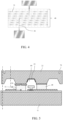
- FIGURE 4 illustrates a top view of a seal ring structure according to some embodiments.
- a width of the seal ring in a cross-sectional direction can be for example, 40-300 ⁇ m, such as 60-100 ⁇ m.
- the lateral electrical connection line 50 extends through the seal ring 40 outside the wafer level package.
- a width of the lateral electrical connection line 50 can be for example, 5-30 ⁇ m, such as 10-20 ⁇ m.
- the lateral electrical connection line 50 enables an electrical connection between the device inside the package and an electrical circuit outside the package.
- FIGURE 4 further illustrates that the dummy lines 51 are provided within the seal ring.
- the dummy lines equalize the surface under the seal ring 40.
- the width of the dummy lines 50 can be for example, 1-20 ⁇ m, such as 2-5 ⁇ m.
- the spacing between the dummy lines 51 as well as between the lateral electrical connection line 50 and the dummy lines 51 can be for example, 2-20 ⁇ m, such as 3-10 ⁇ m.
- the thickness of the lateral electrical connection line 50 and the dummy lines 51 can be for example, 0.2-5 ⁇ m, such as 0.5-1 ⁇ m.
- FIGURE 3 illustrates that the package 100 comprises a micro-groove 34 in the second substrate 22.
- the micro-groove enables aligning the micro-ring 33 to the second substrate 22.
- FIGURE 5 illustrates that the package 100 comprises a cavity 60 in the second substrate 22.
- FIGURE 5 illustrates that the package 100 comprises a getter 61 on a surface of the cavity 60.
- the getter can be used to create and maintain vacuum.
- the getter can be a thin film getter.
- the getter absorbs some or all of the gases anticipated to outgas into the cavity, such as water vapour, oxygen, carbon monoxide, carbon dioxide, nitrogen, hydrogen and/or other gases.
- the first substrate 11 and the second substrate 22 comprise silicon or ceramic.
- Silicon is very reliable substrate material as it suffers very little fatigue and can have long service lifetimes without breaking. In single crystal form, silicon has virtually no hysteresis and hence almost no energy dissipation.
- Suitable ceramic substrates are, for example, silicon nitride, aluminium nitride, titanium nitride or silicon carbide.
- Aluminum nitride in the wurtzite structure shows pyroelectric and piezoelectric properties, which enables to produce sensors for example, with sensitivity to normal and shear forces. Titanium nitride exhibits a high electrical conductivity and large elastic modulus.
- the lateral electrical connection line 50 and the dummy lines 51 comprise metal, such as molybdenum, aluminum or copper. These metals enable good and reliable electrical connection in the lateral electrical connection line between the device inside the package and the electrical circuit outside the package.
- the seal ring 40 comprises dielectric material, ceramic material or metal covered with insulation layer.
- the seal ring can comprise for example, silicon dioxide (SiO 2 ), aluminum nitride (A1N), aluminium oxide (Al 2 O 3 ), silicon nitride (Si 3 N 4 ), silicon carbide (SiC) or aluminium oxide (Al 2 O 3 ) coated copper or nickel. Silicon dioxide provides a good wetting surface for the bonding layer 30 and a good electric insulation.
- the micro-rings 33 can comprise, or be formed of, the same material than the seal ring 40, such as silicon dioxide (SiO 2 ), aluminum nitride (AlN), aluminium oxide (Al 2 O 3 ), silicon nitride (Si 3 N 4 ), silicon carbide (SiC) or aluminium oxide (Al 2 O 3 ) coated copper or nickel.
- silicon dioxide SiO 2
- AlN aluminum nitride
- Al 2 O 3 aluminium oxide
- Si 3 N 4 silicon nitride
- SiC silicon carbide
- Al 2 O 3 aluminium oxide coated copper or nickel
- the getter comprises metals that easily absorb gas.
- the getter can comprise at least one of the following: titanium, aluminum, zirconium, boron, cobalt, calcium, strontium or thorium.
- the package 100 comprises a micro-ring pattern 90 on the first substrate 11.
- the micro-ring pattern 90 can comprise for example, silicon (Si), silicon dioxide (SiO 2 ), metal or semiconductor material.
- the micro-ring pattern 90 confines material of the seal ring 40 between micro-rings by pinch-off effect.
- the micro-ring pattern also provides precise gap control due to precise height of the micro-ring pattern.
- the dummy lines 51 can form the micro-ring pattern 90.
- FIGURES 6A and 6B illustrate that a method for forming a wafer level package 100 for a device comprises a method for forming a wafer level package 100 for a device comprising making a lateral electrical connection line 50 (not shown in FIGURES 6A and 6B ) on a surface of a first substrate 11, making a seal ring 40 on the surface of the first substrate 11 and over a portion of the lateral electrical connection line 50, making a first bonding material layer 31 on a surface of the seal ring 40, making a second bonding material layer 32 on a surface of a second substrate 22, and bonding the first bonding material layer 31 with the second bonding material layer 32 to form a bonding layer 30.
- the lateral electrical connection line 50 extends through the seal ring 40 for creating an electrical connection between the device inside the package 100 and an electrical circuit outside the package 100.
- a deposition of layers of the wafer level package 100 can be conducted by a deposition process.
- the deposition process can comprise for example, physical vapor deposition (PVD) or chemical vapor deposition (CVD).
- Thickness of the first bonding material layer 31 and the second material layer 32 can be for example, 0.3-0.8 ⁇ m, such as 0.4 -0.7 ⁇ m each. Also the thickness on the micro-ring 33 can be for example 0.3-0.8 ⁇ m, such as 0.4 -0.7 ⁇ m.
- bonding the first bonding material layer 31 with the second bonding material layer 32 is provided by eutectic bonding.
- temperature can be raised to a value lower than the eutectic temperature of the eutectic alloy. Then, temperature can be maintained constant for short time to reach uniform heating of both first substrate and second substrate. After that, temperature can be increased to a temperature exceeding the eutectic point. Finally, the structure can cool down to a temperature below the eutectic temperature.
- Eutectic bonding does not require use of high contact force during the bonding. Eutectic bonding is less sensitive to surface flatness irregularities, scratches, as well as to particles compared to the direct wafer bonding methods, because the eutectic bonding process goes through a liquid phase.
- eutectic bonding is conducted 10-20 °C above eutectic temperature of a eutectic alloy.
- Aluminum-germanium bonding can be conducted for example, at 390 °C.
- Gold-tin bonding can be conducted for example, at 290 °C.
- Gold-silicon bonding can be conducted for example, at 375 °C.
- Gold-germanium bonding can be conducted for example, at 435 °C.
- bonding the first bonding material layer 31 with the second bonding material layer 32 can be provided by transient liquid phase bonding.
- Transient liquid phase bonding results in an inter-metallic compound bonding layer.
- This advanced type of solder bonding process can form high-quality hermetic seals at lower temperatures than other bonding technologies.
- Transient liquid phase bonding uses one thin layer of metal (typically 1-10 ⁇ m thick) which during a thermal process diffuses into its bonding partner forming an inter-metallic compound layer with re-melting temperature higher than the bonding temperature.
- the inter-metallic compound bonding layer can be formed by using lower bonding temperatures than the bonding temperatures of the most usual eutectic alloys. Thus, the inter-metallic compound bonding layer can be used in applications where lower producing temperatures are needed.
- Transient liquid phase bonding can be conducted in a same manner than eutectic bonding: first, temperature can be raised to a value lower than a bonding temperature. Then, temperature can be maintained constant for short time to reach uniform heating of both first substrate and second substrate. After that, temperature can be increased to a temperature exceeding the bonding temperature. Finally, the structure can cool down to a temperature below the bonding temperature.
- transient liquid phase bonding can be conducted at temperature of 150-300 °C.
- bonding the first bonding material layer 31 with the second bonding material layer 32 can be provided by glass frit wafer bonding.
- Glass frit wafer bonding uses as intermediate layer for bonding a low melting point glass. The bond occurs by heating the substrates with applied contact force.
- Bonding can be conducted in a bonding chamber.
- a controlled vacuum pressure can be formed in the bonding chamber.
- the vacuum pressure can be for example, 0.8 10 -5 mbar.
- One or more inert gases, such as argon and nitrogen, can be introduced to the bonding chamber.
- FIGURE 9A illustrates that the seal ring 40 can be deposited on the first substrate 11. Thickness of the seal ring 40 can be for example, 0.3-1 ⁇ m, such as 0.4-0.6 ⁇ m.
- the method comprises providing of a plurality of micro-rings 33 within the seal ring 40.
- micro-rings can be provided within the seal ring by patterning of the seal ring as illustrated in FIGURE 9B .
- the micro-rings confine at least a portion of the material of the bonding layer 30 between the micro-rings 33.
- FIGURES 7A-7C illustrate a cross-sectional view of the micro-ring 33 designs according to some embodiments.
- the micro-rings are provided within the seal ring 40.
- a first bonding material layer 31 is provided on the seal ring 40 and the micro-rings 33.
- a height of the micro-ring can be for example, 0.5 ⁇ m.
- a width of a gap between the micro-rings and form of the micro-rings can be selected for example, according to preferred properties of the sealing structure or process parameters.
- FIGURE 8 illustrates a top view of a micro-ring 33 structure according to some embodiments.
- a plurality of micro-rings 33 such as two, can be provided within the seal ring 40.
- a width of the micro-ring can be for example, 0.5 to 15 ⁇ m.
- the method can comprise depositing an oxide layer.
- the oxide layer can be deposited on for example, the first substrate 11, the second substrate 22, the first bonding material layer 31, the second material layer 32, the seal ring 40 and the lateral electrical connection line 50.
- the oxide layers can be grown by thermal oxidation in which a layer is exposed to oxygen and/or steam to grow a thin surface layer on the layer.
- the oxide layers of the (typically silicon) the first substrate 11 and the second substrate 22 can comprise silicon dioxide (SiO 2 ). The oxide layers prevent the layers of the wafer level package from oxidation.
- FIGURES 9B, 9D and 10B illustrate that according to some embodiments, the method comprises patterning of the seal ring 40, the oxide layer, the first material layer 31 and/or the second material layer 32.
- Patterning can be used for removing areas from the layers of the wafer level package. Patterning can be conducted by lithography, electron beam lithography, ion beam lithography, ion track technology, X-ray lithography or diamond patterning.
- the method comprises removing of oxide layers before bonding of the first bonding material layer 21 and the second bonding material layer 22 before bonding the first bonding material 31 layer with the second bonding material layer 32.
- the oxide layers can be removed for example, by plasma cleaning, wet chemical etching or dry chemical etching.
- FIGURE 12D illustrates that according to some embodiments, the method comprises forming of a cavity 60 in the second substrate 22.
- the cavity can be formed by for example, silicon wet or dry etching.
- the method comprises forming a getter 61 on the cavity 60 in the second substrate 22.
- the getter 61 can be formed by getter deposition process.
- the getter can be deposited for example, by using sputtering, resistive evaporation, e-beam evaporation or other suitable deposition technique.
- FIGURES 9A-9D illustrates a manufacturing method of a first structure 10 according to some embodiments.
- the lateral electrical connection line 50 and the dummy lines 51 can be provided on a surface of the first substrate 11 (not illustrated).
- a seal ring 40 can be deposited on the lateral electrical connection line 50 and the dummy lines 51 as illustrated in FIGURE 9A .
- the seal ring 40 can be patterned as illustrated in FIGURE 9B .
- a first bonding material layer 31 can be deposited on the seal ring as illustrated in FIGURE 9C .
- the seal ring layer and the first bonding material layer can be patterned as illustrated in FIGURE 9D .
- FIGURES 10A and 10B illustrate a manufacturing method of a second structure 20 according to some embodiments.
- a second bonding material layer 32 is deposited on a second substrate 22 as illustrated FIGURE 10A .
- the second bonding material layer is patterned as illustrated FIGURE 10B .
- FIGURES 11A-11B illustrate a manufacturing method of a first structure 10 according to some embodiments of the present invention.
- an oxide layer 80 such as silicon oxide (SiO 2 )
- SiO 2 silicon oxide
- the lateral electrical connection line 50 and the dummy lines 51 is provided on the oxide layer ( FIGURE 11B ).
- a metal or metal oxide layer 80 such as aluminum or aluminum oxide (Al 2 O 3 ) layer
- Al 2 O 3 aluminum oxide
- the first bonding material layer 31 can be deposited on the metal or metal oxide layer.
- a metal or metal oxide layer 80, such as aluminum or aluminum oxide (Al 2 O 3 ) layer is deposited on the first bonding material layer 31 as illustrated in FIGURE 11C .
- FIGURES 12A-12E illustrate a manufacturing method of a second structure 20 according to some embodiments.
- an align-mark 70 is generated on a back side of the second substrate 22 and chip numbering can be conducted ( FIGURE 12A ).
- the second bonding material layer 32 is provided on the second substrate 22, and the first bonding material layer is patterned as illustrated in FIGURE 12B .
- an oxide layer 80 can be deposited on the first bonding material layer 31.
- the oxide layer 80 can be patterned ( FIGURE 12C ).
- the oxide layers 80 can be removed for example, by plasma cleaning, wet chemical etching or dry chemical etching before bonding.
- the cavity 60 can be formed in the second substrate 22 by silicon wet or dry etching ( FIGURE 12D ).
- a getter 61 is deposited on a surface of the cavity 60 as illustrated in FIGURE 12E .
- FIGURES 13A-13C illustrate a manufacturing method of a first structure 10 according to some embodiments of the present invention.
- the lateral electrical connection line 50 and optionally also the dummy lines 51 can be provided on a surface of a first substrate 11 (not illustrated).
- a micro-ring pattern 90 is made on the first substrate 11 as illustrated in FIGURE 13A .
- a seal ring 40 is deposited on the micro-ring pattern 90 and the surface of the first substrate 11 and over a portion of the lateral electrical connection line 50 ( FIGURE 13B ).
- the seal ring 40 reproduces the form of the micro-ring pattern 90.
- a first bonding material layer 31 can be deposited on the seal ring as illustrated in FIGURE 13C .
- the dummy lines 51 can form the micro-ring pattern 90.
- the sealing structure is for a MEMS device.
- the sealing structure can be used in other devices, such as automotive devices, e.g. lidar components and tire pressure sensors, RF components, e.g. switches, filters, inductors and antennas, passive photonic devices, e.g. silicon wave guide and modulator, microspectrometer components and plasmonics devices.
- the mechanical bond in formed exclusively by the bonding layer 30 such that the micro-rings 33 do not participate in forming the mechanical bond.
Landscapes
- Engineering & Computer Science (AREA)
- Microelectronics & Electronic Packaging (AREA)
- Manufacturing & Machinery (AREA)
- Computer Hardware Design (AREA)
- Chemical & Material Sciences (AREA)
- Analytical Chemistry (AREA)
- Micromachines (AREA)
Description
- The invention relates to a wafer level package for a device, in particular to a wafer level package for microelectromechanical systems (MEMS).
- Microelectromechanical systems (MEMS) are miniaturized mechanical and electro-mechanical elements, such as devices and structures that are made using the techniques of microfabrication. MEMS are comprised of components between 1 and 100 micrometers in size and MEMS devices generally range in size from 20 micrometers to a millimeter.
- Due to their small size, composition and extremely demanding manufacturing methods, MEMS devices are susceptible to electrical failures and mechanical damages. Therefore, MEMS devices need to be packaged, for example by sealing the device between two wafers connected by a seal ring. Non-uniformity of bonding temperature and bonding force used in bonding the two wafers together may cause low quality of MEMS. Due to non-uniform melting near eutectic temperature and bonding force, excessive squeezing of bonding material out from a seal ring area of MEMS may occur. This may lead to void formation and variation in gap dimensions between wafers. In addition, generally used bonding techniques provide only a small process window and may cause bonding misalignments. Moreover, electrical connection is generally formed by a difficult and complex structure by pads inside and outside packaging.
- Thus, there is need for improved structures and manufacturing methods of a sealing structure of a wafer packaging.
WO 03/088347 A2 present claim 1 and a method according to the preamble of present claim 9. - The invention is defined by the features of the independent claims. Some specific embodiments are defined in the dependent claims.
- According to a first aspect of the present invention, there is provided a wafer level package for a device, the package comprising: a first substrate and a second substrate, a sealing structure comprising a seal ring and a bonding layer between the first substrate and the second substrate, and a lateral electrical connection line on a surface of the first substrate, which lateral electrical connection line extends through the seal ring for creating an electrical connection between the device inside the package and an electrical circuit outside the package. The package comprises a plurality of micro-rings within the seal ring, wherein at least a portion of the material of the bonding layer is located between the micro-rings.
- According to one embodiment of the present invention, the bonding layer is on a surface of the second substrate.
- According to one embodiment of the present invention, the micro-rings are formed by protrusions on the surface of the seal ring.
- According to one embodiment of the present invention, the seal ring comprises dielectric material.
- According to one embodiment of the present invention, the package comprises a micro-ring pattern on the first substrate.
- According to a second aspect of the present invention, there is provided a method for forming a wafer level package for a device comprising: making a lateral electrical connection line on a surface of a first substrate, making a seal ring on the surface of the first substrate and over a portion of the lateral electrical connection line, making a first bonding material layer on a surface of the seal ring, making a second bonding material layer on a surface of a second substrate, and bonding the first bonding material layer with the second bonding material layer to form a bonding layer, wherein the lateral electrical connection line extends through the seal ring for creating an electrical connection between the device inside the package and an electrical circuit outside the package. The method comprises providing of a plurality of micro-rings within the seal ring to confine at least a portion of the material of the bonding layer between the micro-rings when said material melts during the bonding process.
- According to one embodiment of the present invention, bonding the first bonding material layer with the second bonding material layer is provided by eutectic bonding, transient liquid phase bonding or glass frit wafer bonding.
- According to one embodiment of the present invention, the wafer level package is for a MEMS device.
- The present invention provides several advantages. The invention provides a lateral electrical connection line, which extends through a seal ring for creating an electrical connection between a device inside a package and an electrical circuit outside the package. Moreover, a squeezing control of a bonding layer between bonding substrates, such as germanium-aluminum alloy melt, is provided by micro-rings. In addition, the micro-rings increase process window in the bonding of the substrates, especially in eutectic bonding of the substrates. The micro-rings also provide a precise gap due to a precise height of the micro-rings, which gap is free from temperature and pressure non-uniformities, such as voids. The invention provides a good and uniform bonding strength for a wafer level package. The invention also reduces slip misalignment between the bonding substrates due to local indentation and increased friction, hence improving bonding quality.
-
-
FIGURE 1 illustrates a part of a seal ring in a wafer level package in accordance with at least some embodiments of the present invention; -
FIGURE 2 illustrates a part of a seal ring in a wafer level package for a device in accordance with at least some embodiments of the present invention; -
FIGURE 3 illustrates a part of a seal ring in a wafer level package for a device in accordance with at least some embodiments of the present invention; -
FIGURE 4 illustrates a top view of a part of a seal ring structure in accordance with at least some embodiments of the present invention; -
FIGURE 5 illustrates a wafer level package for a device in accordance with at least some embodiments of the present invention; -
FIGURES 6A and 6B illustrate a method for forming a wafer level package for a device in accordance with at least some embodiments of the present invention; -
FIGURES 7A-7C illustrate a cross-sectional view of the micro-ring designs in accordance with at least some embodiments of the present invention; -
FIGURE 8 illustrates a top view of a micro-ring structure in accordance with at least some embodiments of the present invention; -
FIGURES 9A-9D illustrate a manufacturing method of a first structure in accordance with at least some embodiments of the present invention; -
FIGURES 10A and 10B illustrate a manufacturing method of a second structure in accordance with at least some embodiments of the present invention; -
FIGURES 11A-11C illustrate a manufacturing method of a first structure in accordance with at least some embodiments of the present invention; -
FIGURES 12A-12E illustrate a manufacturing method of a second structure in accordance with at least some embodiments of the present invention, and -
FIGURES 13A-13C illustrate a manufacturing method of a first structure in accordance with at least some embodiments of the present invention. - In the present context, the term "substrate" comprises a wafer, such as a MEMS device wafer and a cap wafer.
- The object of at least of some embodiments of the present invention is to provide a high quality wafer level package, especially for a microelectromechanical systems (MEMS) device, which sealing structure provides good electrical connection and precise gap control free from temperature and pressure non-uniformities, such as voids.
-
FIGURE 1 illustrates a part of awafer level package 100 for a device according to some embodiments. Thewafer level package 100 for a device comprises: afirst substrate 11 and asecond substrate 22, a sealing structure comprising aseal ring 40 and abonding layer 30 between thefirst substrate 11 and thesecond substrate 22, and a lateralelectrical connection line 50 and/ordummy line 51 on a surface of thefirst substrate 11, which lateralelectrical connection line 50 extends through theseal ring 40 for creating an electrical connection between the device inside the package and an electrical circuit outside the package. Thus, electrical connection is formed by simple and reliable structure. In an embodiment, the lateralelectrical connection line 50 and thedummy line 51 have a same composition but the difference is in the pattern and location as well as in the purpose of the structures. Whereas the lateralelectrical connection line 50 is for creating electrical contact between the device inside the packages and external circuitry outside the package, thedummy lines 51 are there to equalize the surface under theseal ring 40 and around the lateralelectrical connection line 50 so that the thickness of theseal ring 40 is easier to control. -
FIGURES 1-3 illustrate that thewafer level package 100 for a device comprises abonding layer 30 on a surface of thesecond substrate 22. Thebonding layer 30 enables bonding of thefirst substrate 11 and the second substrate 12 of thewafer lever package 100 together. - According to some embodiments, the
bonding layer 30 comprises a eutectic alloy. The eutectic alloy can comprise two or more metals. Suitable eutectic alloys include, for example, germanium-aluminum, gold-tin, gold-germanium, gold-silicon, gold-indium or copper-tin alloy. - According to some other embodiments, the
bonding layer 30 is an inter-metallic compound bonding layer. The inter-metallic compound bonding layer can comprise metal alloy, such as copper-tin, gold-indium or silver-tin alloy. - Alternatively, the
bonding layer 30 can be a glass frit wafer bonding layer. Glass frit bonding has a high tolerance to surface roughness and can incorporate high topography of the substrates. -
FIGURES 1-3 illustrate that thepackage 100 comprises a plurality ofmicro-rings 33, such as two, three, four or more, within theseal ring 40. The micro-rings confine material, such as metal melt, of thebonding layer 30 between micro-rings by pinch-off effect and provide controlled horizontal squeezing of the material of thebonding layer 30 outside the micro-rings. The micro-rings also provide precise gap control due to precise height of the micro-rings. The micro-rings provide the gap which is free from temperature and pressure non-uniformities, such as voids, due to uniform flowing of the bonding material to the gap. The bonding layer can extend all way on the surface of the second substructure (not illustrated). In addition, the micro-rings increases process window of bonding. Moreover, they reduce slip misalignment between the first substrate and the second substrate due to local indentation and increased friction. - According to some embodiments, the micro-rings 33 are formed by protrusions on the surface of the
seal ring 40. The micro-rings 33 can be formed by continuous rings extending on the surface of theseal ring 40. The micro-rings 33 can thus extend around the cavity. -
FIGURE 4 illustrates a top view of a seal ring structure according to some embodiments. A width of the seal ring in a cross-sectional direction can be for example, 40-300 µm, such as 60-100 µm. The lateralelectrical connection line 50 extends through theseal ring 40 outside the wafer level package. A width of the lateralelectrical connection line 50 can be for example, 5-30 µm, such as 10-20 µm. The lateralelectrical connection line 50 enables an electrical connection between the device inside the package and an electrical circuit outside the package. -
FIGURE 4 further illustrates that the dummy lines 51 are provided within the seal ring. The dummy lines equalize the surface under theseal ring 40. The width of the dummy lines 50 can be for example, 1-20 µm, such as 2-5 µm. The spacing between the dummy lines 51 as well as between the lateralelectrical connection line 50 and the dummy lines 51 can be for example, 2-20 µm, such as 3-10 µm. The thickness of the lateralelectrical connection line 50 and the dummy lines 51 can be for example, 0.2-5 µm, such as 0.5-1 µm. -
FIGURE 3 illustrates that thepackage 100 comprises a micro-groove 34 in thesecond substrate 22. The micro-groove enables aligning the micro-ring 33 to thesecond substrate 22. -
FIGURE 5 illustrates that thepackage 100 comprises acavity 60 in thesecond substrate 22. - In addition,
FIGURE 5 illustrates that thepackage 100 comprises agetter 61 on a surface of thecavity 60. The getter can be used to create and maintain vacuum. The getter can be a thin film getter. The getter absorbs some or all of the gases anticipated to outgas into the cavity, such as water vapour, oxygen, carbon monoxide, carbon dioxide, nitrogen, hydrogen and/or other gases. - In an embodiment, the
first substrate 11 and thesecond substrate 22 comprise silicon or ceramic. Silicon is very reliable substrate material as it suffers very little fatigue and can have long service lifetimes without breaking. In single crystal form, silicon has virtually no hysteresis and hence almost no energy dissipation. Suitable ceramic substrates are, for example, silicon nitride, aluminium nitride, titanium nitride or silicon carbide. Aluminum nitride in the wurtzite structure shows pyroelectric and piezoelectric properties, which enables to produce sensors for example, with sensitivity to normal and shear forces. Titanium nitride exhibits a high electrical conductivity and large elastic modulus. - According to an embodiment, the lateral
electrical connection line 50 and the dummy lines 51 comprise metal, such as molybdenum, aluminum or copper. These metals enable good and reliable electrical connection in the lateral electrical connection line between the device inside the package and the electrical circuit outside the package. - According to an embodiment, the
seal ring 40 comprises dielectric material, ceramic material or metal covered with insulation layer. The seal ring can comprise for example, silicon dioxide (SiO2), aluminum nitride (A1N), aluminium oxide (Al2O3), silicon nitride (Si3N4), silicon carbide (SiC) or aluminium oxide (Al2O3) coated copper or nickel. Silicon dioxide provides a good wetting surface for thebonding layer 30 and a good electric insulation. - The micro-rings 33 can comprise, or be formed of, the same material than the
seal ring 40, such as silicon dioxide (SiO2), aluminum nitride (AlN), aluminium oxide (Al2O3), silicon nitride (Si3N4), silicon carbide (SiC) or aluminium oxide (Al2O3) coated copper or nickel. - According to an embodiment, the getter comprises metals that easily absorb gas. For example, the getter can comprise at least one of the following: titanium, aluminum, zirconium, boron, cobalt, calcium, strontium or thorium.
- According to an embodiment, the
package 100 comprises amicro-ring pattern 90 on thefirst substrate 11. Themicro-ring pattern 90 can comprise for example, silicon (Si), silicon dioxide (SiO2), metal or semiconductor material. Themicro-ring pattern 90 confines material of theseal ring 40 between micro-rings by pinch-off effect. The micro-ring pattern also provides precise gap control due to precise height of the micro-ring pattern. - Alternatively, the dummy lines 51 can form the
micro-ring pattern 90. -
FIGURES 6A and 6B illustrate that a method for forming awafer level package 100 for a device comprises a method for forming awafer level package 100 for a device comprising making a lateral electrical connection line 50 (not shown inFIGURES 6A and 6B ) on a surface of afirst substrate 11, making aseal ring 40 on the surface of thefirst substrate 11 and over a portion of the lateralelectrical connection line 50, making a firstbonding material layer 31 on a surface of theseal ring 40, making a secondbonding material layer 32 on a surface of asecond substrate 22, and bonding the firstbonding material layer 31 with the secondbonding material layer 32 to form abonding layer 30. The lateralelectrical connection line 50 extends through theseal ring 40 for creating an electrical connection between the device inside thepackage 100 and an electrical circuit outside thepackage 100. - A deposition of layers of the
wafer level package 100, such as a firstbonding material layer 31 and the secondbonding material layer 32, can be conducted by a deposition process. The deposition process can comprise for example, physical vapor deposition (PVD) or chemical vapor deposition (CVD). - Thickness of the first
bonding material layer 31 and thesecond material layer 32 can be for example, 0.3-0.8 µm, such as 0.4 -0.7 µm each. Also the thickness on the micro-ring 33 can be for example 0.3-0.8 µm, such as 0.4 -0.7 µm. - According to some embodiments, bonding the first
bonding material layer 31 with the secondbonding material layer 32 is provided by eutectic bonding. First, temperature can be raised to a value lower than the eutectic temperature of the eutectic alloy. Then, temperature can be maintained constant for short time to reach uniform heating of both first substrate and second substrate. After that, temperature can be increased to a temperature exceeding the eutectic point. Finally, the structure can cool down to a temperature below the eutectic temperature. - Eutectic bonding does not require use of high contact force during the bonding. Eutectic bonding is less sensitive to surface flatness irregularities, scratches, as well as to particles compared to the direct wafer bonding methods, because the eutectic bonding process goes through a liquid phase.
- According to some embodiments, eutectic bonding is conducted 10-20 °C above eutectic temperature of a eutectic alloy. Aluminum-germanium bonding can be conducted for example, at 390 °C. Gold-tin bonding can be conducted for example, at 290 °C. Gold-silicon bonding can be conducted for example, at 375 °C. Gold-germanium bonding can be conducted for example, at 435 °C.
- Alternatively, bonding the first
bonding material layer 31 with the secondbonding material layer 32 can be provided by transient liquid phase bonding. Transient liquid phase bonding results in an inter-metallic compound bonding layer. This advanced type of solder bonding process can form high-quality hermetic seals at lower temperatures than other bonding technologies. Transient liquid phase bonding uses one thin layer of metal (typically 1-10 µm thick) which during a thermal process diffuses into its bonding partner forming an inter-metallic compound layer with re-melting temperature higher than the bonding temperature. The inter-metallic compound bonding layer can be formed by using lower bonding temperatures than the bonding temperatures of the most usual eutectic alloys. Thus, the inter-metallic compound bonding layer can be used in applications where lower producing temperatures are needed. - Transient liquid phase bonding can be conducted in a same manner than eutectic bonding: first, temperature can be raised to a value lower than a bonding temperature. Then, temperature can be maintained constant for short time to reach uniform heating of both first substrate and second substrate. After that, temperature can be increased to a temperature exceeding the bonding temperature. Finally, the structure can cool down to a temperature below the bonding temperature.
- According to some embodiments, transient liquid phase bonding can be conducted at temperature of 150-300 °C.
- Alternatively, bonding the first
bonding material layer 31 with the secondbonding material layer 32 can be provided by glass frit wafer bonding. Glass frit wafer bonding uses as intermediate layer for bonding a low melting point glass. The bond occurs by heating the substrates with applied contact force. - Bonding can be conducted in a bonding chamber. A controlled vacuum pressure can be formed in the bonding chamber. The vacuum pressure can be for example, 0.8 10-5 mbar. One or more inert gases, such as argon and nitrogen, can be introduced to the bonding chamber.
-
FIGURE 9A illustrates that theseal ring 40 can be deposited on thefirst substrate 11. Thickness of theseal ring 40 can be for example, 0.3-1 µm, such as 0.4-0.6 µm. - According to the invention, the method comprises providing of a plurality of
micro-rings 33 within theseal ring 40. According to some embodiments, micro-rings can be provided within the seal ring by patterning of the seal ring as illustrated inFIGURE 9B . The micro-rings confine at least a portion of the material of thebonding layer 30 between the micro-rings 33. -
FIGURES 7A-7C illustrate a cross-sectional view of the micro-ring 33 designs according to some embodiments. The micro-rings are provided within theseal ring 40. A firstbonding material layer 31 is provided on theseal ring 40 and the micro-rings 33. A height of the micro-ring can be for example, 0.5 µm. A width of a gap between the micro-rings and form of the micro-rings can be selected for example, according to preferred properties of the sealing structure or process parameters. -
FIGURE 8 illustrates a top view of a micro-ring 33 structure according to some embodiments. A plurality ofmicro-rings 33, such as two, can be provided within theseal ring 40. A width of the micro-ring can be for example, 0.5 to 15 µm. - According to some embodiments, the method can comprise depositing an oxide layer. The oxide layer can be deposited on for example, the
first substrate 11, thesecond substrate 22, the firstbonding material layer 31, thesecond material layer 32, theseal ring 40 and the lateralelectrical connection line 50. The oxide layers can be grown by thermal oxidation in which a layer is exposed to oxygen and/or steam to grow a thin surface layer on the layer. The oxide layers of the (typically silicon) thefirst substrate 11 and thesecond substrate 22 can comprise silicon dioxide (SiO2). The oxide layers prevent the layers of the wafer level package from oxidation. -
FIGURES 9B, 9D and10B illustrate that according to some embodiments, the method comprises patterning of theseal ring 40, the oxide layer, thefirst material layer 31 and/or thesecond material layer 32. Patterning can be used for removing areas from the layers of the wafer level package. Patterning can be conducted by lithography, electron beam lithography, ion beam lithography, ion track technology, X-ray lithography or diamond patterning. - According to some embodiments, the method comprises removing of oxide layers before bonding of the first bonding material layer 21 and the second
bonding material layer 22 before bonding thefirst bonding material 31 layer with the secondbonding material layer 32. The oxide layers can be removed for example, by plasma cleaning, wet chemical etching or dry chemical etching. -
FIGURE 12D illustrates that according to some embodiments, the method comprises forming of acavity 60 in thesecond substrate 22. The cavity can be formed by for example, silicon wet or dry etching. - According to some embodiments, the method comprises forming a
getter 61 on thecavity 60 in thesecond substrate 22. Thegetter 61 can be formed by getter deposition process. The getter can be deposited for example, by using sputtering, resistive evaporation, e-beam evaporation or other suitable deposition technique. - The method for forming the sealing structure of the wafer packaging for a device will now be discussed in more detail by means of example embodiments.
-
FIGURES 9A-9D illustrates a manufacturing method of afirst structure 10 according to some embodiments. First, the lateralelectrical connection line 50 and the dummy lines 51 can be provided on a surface of the first substrate 11 (not illustrated). Then, aseal ring 40 can be deposited on the lateralelectrical connection line 50 and the dummy lines 51 as illustrated inFIGURE 9A . Theseal ring 40 can be patterned as illustrated inFIGURE 9B . After that, a firstbonding material layer 31 can be deposited on the seal ring as illustrated inFIGURE 9C . Finally, the seal ring layer and the first bonding material layer can be patterned as illustrated inFIGURE 9D . -
FIGURES 10A and 10B illustrate a manufacturing method of asecond structure 20 according to some embodiments. First, a secondbonding material layer 32 is deposited on asecond substrate 22 as illustratedFIGURE 10A . Then, the second bonding material layer is patterned as illustratedFIGURE 10B . -
FIGURES 11A-11B illustrate a manufacturing method of afirst structure 10 according to some embodiments of the present invention. First, anoxide layer 80, such as silicon oxide (SiO2), is generated on afirst substrate 11 as illustrated inFIGURE 11A . Then, the lateralelectrical connection line 50 and the dummy lines 51 is provided on the oxide layer (FIGURE 11B ). After that, a metal ormetal oxide layer 80, such as aluminum or aluminum oxide (Al2O3) layer, can be deposited on the lateral electrical connection line and the dummy lines 51 for preventing the lateral electrical connection line and the dummy lines 51 from oxidation. The firstbonding material layer 31 can be deposited on the metal or metal oxide layer. A metal ormetal oxide layer 80, such as aluminum or aluminum oxide (Al2O3) layer, is deposited on the firstbonding material layer 31 as illustrated inFIGURE 11C . -
FIGURES 12A-12E illustrate a manufacturing method of asecond structure 20 according to some embodiments. First, an align-mark 70 is generated on a back side of thesecond substrate 22 and chip numbering can be conducted (FIGURE 12A ). Then, the secondbonding material layer 32 is provided on thesecond substrate 22, and the first bonding material layer is patterned as illustrated inFIGURE 12B . After that, anoxide layer 80 can be deposited on the firstbonding material layer 31. Theoxide layer 80 can be patterned (FIGURE 12C ). The oxide layers 80 can be removed for example, by plasma cleaning, wet chemical etching or dry chemical etching before bonding. In addition, thecavity 60 can be formed in thesecond substrate 22 by silicon wet or dry etching (FIGURE 12D ). Finally and optionally, agetter 61 is deposited on a surface of thecavity 60 as illustrated inFIGURE 12E . -
FIGURES 13A-13C illustrate a manufacturing method of afirst structure 10 according to some embodiments of the present invention. First, the lateralelectrical connection line 50 and optionally also the dummy lines 51 can be provided on a surface of a first substrate 11 (not illustrated). Then, amicro-ring pattern 90 is made on thefirst substrate 11 as illustrated inFIGURE 13A . After that, aseal ring 40 is deposited on themicro-ring pattern 90 and the surface of thefirst substrate 11 and over a portion of the lateral electrical connection line 50 (FIGURE 13B ). Theseal ring 40 reproduces the form of themicro-ring pattern 90. Finally, a firstbonding material layer 31 can be deposited on the seal ring as illustrated inFIGURE 13C . - Alternatively, the dummy lines 51 can form the
micro-ring pattern 90. - According to some embodiments, the sealing structure is for a MEMS device. However, the sealing structure can be used in other devices, such as automotive devices, e.g. lidar components and tire pressure sensors, RF components, e.g. switches, filters, inductors and antennas, passive photonic devices, e.g. silicon wave guide and modulator, microspectrometer components and plasmonics devices.
- According to at least some embodiments, the mechanical bond in formed exclusively by the
bonding layer 30 such that the micro-rings 33 do not participate in forming the mechanical bond. - Reference throughout this specification to "one embodiment" or "an embodiment" means that a particular feature, structure, or characteristic described in connection with the embodiment is included in at least one embodiment of the present invention. Thus, appearances of the phrases "in one embodiment" or "in an embodiment" in various places throughout this specification are not necessarily all referring to the same embodiment.
- As used herein, a plurality of items, structural elements, compositional elements, and/or materials may be presented in a common list for convenience. However, these lists should be construed as though each member of the list is individually identified as a separate and unique member. Thus, no individual member of such list should be construed as a de facto equivalent of any other member of the same list solely based on their presentation in a common group without indications to the contrary. In addition, various embodiments and example of the present invention may be referred to herein along with alternatives for the various components thereof. It is understood that such embodiments, examples, and alternatives are not to be construed as de facto equivalents of one another, but are to be considered as separate and autonomous representations of the present invention.
- Furthermore, the described features, structures, or characteristics may be combined in any suitable manner in one or more embodiments. In the following description, numerous specific details are provided, such as examples of lengths, widths, shapes, etc., to provide a thorough understanding of embodiments of the invention. One skilled in the relevant art will recognize, however, that the invention can be practiced without one or more of the specific details, or with other methods, components, materials, etc. In other instances, well-known structures, materials, or operations are not shown or described in detail to avoid obscuring aspects of the invention.
- While the forgoing examples are illustrative of the principles of the present invention in one or more particular applications, it will be apparent to those of ordinary skill in the art that numerous modifications in form, usage and details of implementation can be made without the exercise of inventive faculty, and without departing from the principles and concepts of the invention. Accordingly, it is not intended that the invention be limited, except as by the claims set forth below.
- The verbs "to comprise" and "to include" are used in this document as open limitations that neither exclude nor require the existence of also un-recited features. The features recited in depending claims are mutually freely combinable unless otherwise explicitly stated. Furthermore, it is to be understood that the use of "a" or "an", i.e. a singular form, throughout this document does not exclude a plurality.
-
- 10
- first structure
- 11
- first substrate
- 20
- second structure
- 22
- second substrate
- 30
- bonding layer
- 31
- first bonding material layer
- 32
- second bonding material layer
- 33
- micro-ring
- 34
- micro-groove
- 40
- seal ring
- 50
- lateral electrical connection line
- 51
- dummy line
- 60
- cavity
- 61
- getter
- 70
- align mark
- 80
- oxide layer
- 90
- micro-ring pattern
- 100
- wafer level package
Claims (15)
- A wafer level package (100) for a device, the package (100) comprising:- a first substrate (11) and a second substrate (22),- a sealing structure comprising a seal ring (40) and a bonding layer (30) between the first substrate (11) and the second substrate (22), and- a lateral electrical connection line (50) on a surface of the first substrate (11), which lateral electrical connection line (50) extends through the seal ring (40) for creating an electrical connection between the device inside the package (100) and an electrical circuit outside the package (100),characterized in that the package (100) comprises a plurality of micro-rings (33) within the seal ring (40), wherein at least a portion of the material of the bonding layer (30) is located between the micro-rings (33).
- The wafer level package (100) of claim 1, wherein the bonding layer (30) is on a surface of the second substrate (22).
- The wafer level package (100) of any one of the preceding claims, wherein the micro-rings (33) are formed by protrusions on the surface of the seal ring (40).
- The wafer level package (100) of any one of the preceding claims, wherein the seal ring (40) comprises dielectric material.
- The wafer level package (100) of any one of the preceding claims, wherein the package (100) comprises a cavity (60) in the second substrate (22).
- The wafer level package (100) of claim 5, wherein the package (100) comprises a getter (61) on a surface of the cavity (60).
- The wafer level package (100) of any one of the preceding claims, wherein the package (100) comprises a micro-ring pattern (90) on the first substrate (11).
- The wafer level package (100) of any one of the preceding claims, wherein the package (100) is for a MEMS device.
- A method for forming a wafer level package (100) for a device comprising:- making a lateral electrical connection line (50) on a surface of a first substrate (11),- making a seal ring (40) on the surface of the first substrate (11) and over a portion of the lateral electrical connection line (50),- making a first bonding material layer (31) on a surface of the seal ring (40),- making a second bonding material layer (32) on a surface of a second substrate (22), and- bonding the first bonding material layer (31) with the second bonding material layer (32) to form a bonding layer (30),wherein the lateral electrical connection line (50) extends through the seal ring (40) for creating an electrical connection between the device inside the package (100) and an electrical circuit outside the package (100),characterized in that the method comprises providing of a plurality of micro-rings (33) within the seal ring (40) to confine at least a portion of the material of the bonding layer (30) between the micro-rings (33).
- The method of claim 9, wherein the seal ring (40) comprises dielectric material and the micro-rings (33) are formed by protrusions on the surface of the seal ring (40).
- The method of claim 9 or 10, wherein the method comprises forming a cavity (60) in the second substrate (22) and a getter (61) on the surface of the cavity (60) by getter deposition process.
- The method of any one of the preceding claims 9 to 11, wherein bonding the first bonding material layer (31) with the second bonding material layer (32) is provided by eutectic bonding, transient liquid phase bonding or glass frit wafer bonding.
- The method of claim 12, wherein eutectic bonding is conducted 10-20 °C above eutectic temperature of a eutectic alloy or transient liquid phase bonding is conducted at temperature of 150-300 °C.
- The method of any one of the preceding claims 9 to 13, wherein the method comprises providing a micro-ring pattern (90) on the first substrate (11).
- The method of any one of the preceding claims 9 to 14, wherein the wafer level package (100) is for a MEMS device.
Applications Claiming Priority (2)
| Application Number | Priority Date | Filing Date | Title |
|---|---|---|---|
| FI20205075A FI131434B1 (en) | 2020-01-24 | 2020-01-24 | Disk level capsule for a device |
| PCT/FI2021/050044 WO2021148722A1 (en) | 2020-01-24 | 2021-01-25 | Wafer level package for device |
Publications (3)
| Publication Number | Publication Date |
|---|---|
| EP4093698A1 EP4093698A1 (en) | 2022-11-30 |
| EP4093698B1 true EP4093698B1 (en) | 2024-03-06 |
| EP4093698C0 EP4093698C0 (en) | 2024-03-06 |
Family
ID=74494938
Family Applications (1)
| Application Number | Title | Priority Date | Filing Date |
|---|---|---|---|
| EP21702701.0A Active EP4093698B1 (en) | 2020-01-24 | 2021-01-25 | Wafer level package for device |
Country Status (5)
| Country | Link |
|---|---|
| US (1) | US12209012B2 (en) |
| EP (1) | EP4093698B1 (en) |
| JP (1) | JP7682186B2 (en) |
| FI (1) | FI131434B1 (en) |
| WO (1) | WO2021148722A1 (en) |
Families Citing this family (2)
| Publication number | Priority date | Publication date | Assignee | Title |
|---|---|---|---|---|
| FI20205914A1 (en) | 2020-09-21 | 2022-03-22 | Teknologian Tutkimuskeskus Vtt Oy | Disc level component packaging |
| TWI862281B (en) * | 2023-11-16 | 2024-11-11 | 世界先進積體電路股份有限公司 | Micro-electro-mechanical system package and fabrication method thereof |
Family Cites Families (19)
| Publication number | Priority date | Publication date | Assignee | Title |
|---|---|---|---|---|
| JPS5685955U (en) * | 1979-12-06 | 1981-07-10 | ||
| JPS5685955A (en) | 1979-12-14 | 1981-07-13 | Hitachi Ltd | Control signal transfer system |
| JPH09307122A (en) * | 1996-05-17 | 1997-11-28 | Shinko Electric Ind Co Ltd | Optical element module |
| US6406636B1 (en) * | 1999-06-02 | 2002-06-18 | Megasense, Inc. | Methods for wafer to wafer bonding using microstructures |
| US20020179921A1 (en) * | 2001-06-02 | 2002-12-05 | Cohn Michael B. | Compliant hermetic package |
| EP1495491B1 (en) | 2002-04-15 | 2020-12-16 | Schott AG | Method for connecting substrates and composite element |
| US7354799B2 (en) * | 2005-11-08 | 2008-04-08 | Intel Corporation | Methods for anchoring a seal ring to a substrate using vias and assemblies including an anchored seal ring |
| DE102005053722B4 (en) | 2005-11-10 | 2007-08-16 | Fraunhofer-Gesellschaft zur Förderung der angewandten Forschung e.V. | Cover wafer, in the microsystem technology usable component with such a wafer and soldering method for connecting corresponding component parts |
| US8736039B2 (en) * | 2006-10-06 | 2014-05-27 | Taiwan Semiconductor Manufacturing Co., Ltd. | Stacked structures and methods of forming stacked structures |
| JP2008218811A (en) * | 2007-03-06 | 2008-09-18 | Hitachi Metals Ltd | Functional device package |
| US7662669B2 (en) * | 2007-07-24 | 2010-02-16 | Northrop Grumman Space & Mission Systems Corp. | Method of exposing circuit lateral interconnect contacts by wafer saw |
| DE102009046687A1 (en) * | 2009-11-13 | 2011-05-19 | Robert Bosch Gmbh | Micromechanical method and corresponding arrangement for bonding semiconductor substrates and corresponding bonded semiconductor chip |
| US20120319220A1 (en) * | 2009-12-11 | 2012-12-20 | Pioneer Micro Technology Corporation | Method of bonding semiconductor substrate and mems device |
| WO2012171663A1 (en) * | 2011-06-15 | 2012-12-20 | Eth Zurich | Low-temperature wafer-level packaging and direct electrical interconnection |
| US9556020B2 (en) * | 2013-09-11 | 2017-01-31 | Said Emre Alper | Method of wafer-level hermetic packaging with vertical feedthroughs |
| KR20150132611A (en) * | 2014-05-15 | 2015-11-26 | (주)유우일렉트로닉스 | Wafer level packaging device for controlling field of view |
| WO2017164816A1 (en) * | 2016-03-24 | 2017-09-28 | Agency For Science, Technology And Research | A through silicon interposer wafer and method of manufacturing the same |
| JP2018006577A (en) * | 2016-07-01 | 2018-01-11 | 株式会社デンソー | Manufacturing method for semiconductor device |
| US11004757B2 (en) * | 2018-05-14 | 2021-05-11 | Invensas Bonding Technologies, Inc. | Bonded structures |
-
2020
- 2020-01-24 FI FI20205075A patent/FI131434B1/en active
-
2021
- 2021-01-25 US US17/792,777 patent/US12209012B2/en active Active
- 2021-01-25 JP JP2022544678A patent/JP7682186B2/en active Active
- 2021-01-25 EP EP21702701.0A patent/EP4093698B1/en active Active
- 2021-01-25 WO PCT/FI2021/050044 patent/WO2021148722A1/en not_active Ceased
Also Published As
| Publication number | Publication date |
|---|---|
| JP7682186B2 (en) | 2025-05-23 |
| EP4093698A1 (en) | 2022-11-30 |
| WO2021148722A1 (en) | 2021-07-29 |
| EP4093698C0 (en) | 2024-03-06 |
| FI131434B1 (en) | 2025-04-22 |
| FI20205075A1 (en) | 2021-07-25 |
| JP2023514069A (en) | 2023-04-05 |
| US20230050181A1 (en) | 2023-02-16 |
| US12209012B2 (en) | 2025-01-28 |
Similar Documents
| Publication | Publication Date | Title |
|---|---|---|
| JP3864134B2 (en) | Low temperature antioxidant hermetic sealing method | |
| EP1720204B1 (en) | Transient liquid phase eutectic bonding | |
| US7164199B2 (en) | Device packages with low stress assembly process | |
| US8293582B2 (en) | Method of substrate bonding with bonding material having rare Earth metal | |
| JP3126977B2 (en) | Reinforced direct bond copper structure | |
| JP4495711B2 (en) | Functional element and manufacturing method thereof | |
| US12209012B2 (en) | Wafer level package for device | |
| WO2007078472A1 (en) | Wafer level hermetic bond using metal alloy with raised feature | |
| TW200406934A (en) | Semiconductor component and its production method | |
| KR101364623B1 (en) | Process for manufacturing micromechanical devices containing a getter material and devices so manufactured | |
| US9287237B2 (en) | Hermetically sealed wafer packages | |
| WO1997005757A1 (en) | Diamond electronic packages featuring bonded metal | |
| EP4214150B1 (en) | Wafer level package for device | |
| Knechtel | Glass frit wafer bonding | |
| CN1802235A (en) | Method of soldering or brazing articles having surfaces that are difficult to bond | |
| US7115182B2 (en) | Anodic bonding process for ceramics | |
| US20260091974A1 (en) | Wafer level package for device | |
| Sood et al. | Metal Inter-Diffusion and Eutectic Wafer Bonding Processes for Advanced Mems Packaging | |
| CN122026850A (en) | Cavity structure of wafer level packaging crystal oscillator and metal hot-press bonding method | |
| Bonding | A. Adhesive and Anodic Bonding| 3 | |
| KR20140082070A (en) | Wafer Level Hermetic Package and Wafer Level Hermetic Packaging Method |
Legal Events
| Date | Code | Title | Description |
|---|---|---|---|
| STAA | Information on the status of an ep patent application or granted ep patent |
Free format text: STATUS: UNKNOWN |
|
| STAA | Information on the status of an ep patent application or granted ep patent |
Free format text: STATUS: THE INTERNATIONAL PUBLICATION HAS BEEN MADE |
|
| PUAI | Public reference made under article 153(3) epc to a published international application that has entered the european phase |
Free format text: ORIGINAL CODE: 0009012 |
|
| STAA | Information on the status of an ep patent application or granted ep patent |
Free format text: STATUS: REQUEST FOR EXAMINATION WAS MADE |
|
| 17P | Request for examination filed |
Effective date: 20220823 |
|
| AK | Designated contracting states |
Kind code of ref document: A1 Designated state(s): AL AT BE BG CH CY CZ DE DK EE ES FI FR GB GR HR HU IE IS IT LI LT LU LV MC MK MT NL NO PL PT RO RS SE SI SK SM TR |
|
| DAV | Request for validation of the european patent (deleted) | ||
| DAX | Request for extension of the european patent (deleted) | ||
| GRAP | Despatch of communication of intention to grant a patent |
Free format text: ORIGINAL CODE: EPIDOSNIGR1 |
|
| STAA | Information on the status of an ep patent application or granted ep patent |
Free format text: STATUS: GRANT OF PATENT IS INTENDED |
|
| INTG | Intention to grant announced |
Effective date: 20231010 |
|
| GRAS | Grant fee paid |
Free format text: ORIGINAL CODE: EPIDOSNIGR3 |
|
| GRAA | (expected) grant |
Free format text: ORIGINAL CODE: 0009210 |
|
| STAA | Information on the status of an ep patent application or granted ep patent |
Free format text: STATUS: THE PATENT HAS BEEN GRANTED |
|
| AK | Designated contracting states |
Kind code of ref document: B1 Designated state(s): AL AT BE BG CH CY CZ DE DK EE ES FI FR GB GR HR HU IE IS IT LI LT LU LV MC MK MT NL NO PL PT RO RS SE SI SK SM TR |
|
| REG | Reference to a national code |
Ref country code: CH Ref legal event code: EP |
|
| REG | Reference to a national code |
Ref country code: DE Ref legal event code: R096 Ref document number: 602021010110 Country of ref document: DE |
|
| REG | Reference to a national code |
Ref country code: IE Ref legal event code: FG4D |
|
| U01 | Request for unitary effect filed |
Effective date: 20240325 |
|
| U07 | Unitary effect registered |
Designated state(s): AT BE BG DE DK EE FI FR IT LT LU LV MT NL PT SE SI Effective date: 20240403 |
|
| PG25 | Lapsed in a contracting state [announced via postgrant information from national office to epo] |
Ref country code: GR Free format text: LAPSE BECAUSE OF FAILURE TO SUBMIT A TRANSLATION OF THE DESCRIPTION OR TO PAY THE FEE WITHIN THE PRESCRIBED TIME-LIMIT Effective date: 20240607 |
|
| PG25 | Lapsed in a contracting state [announced via postgrant information from national office to epo] |
Ref country code: RS Free format text: LAPSE BECAUSE OF FAILURE TO SUBMIT A TRANSLATION OF THE DESCRIPTION OR TO PAY THE FEE WITHIN THE PRESCRIBED TIME-LIMIT Effective date: 20240606 Ref country code: HR Free format text: LAPSE BECAUSE OF FAILURE TO SUBMIT A TRANSLATION OF THE DESCRIPTION OR TO PAY THE FEE WITHIN THE PRESCRIBED TIME-LIMIT Effective date: 20240306 |
|
| PG25 | Lapsed in a contracting state [announced via postgrant information from national office to epo] |
Ref country code: ES Free format text: LAPSE BECAUSE OF FAILURE TO SUBMIT A TRANSLATION OF THE DESCRIPTION OR TO PAY THE FEE WITHIN THE PRESCRIBED TIME-LIMIT Effective date: 20240306 |
|
| PG25 | Lapsed in a contracting state [announced via postgrant information from national office to epo] |
Ref country code: RS Free format text: LAPSE BECAUSE OF FAILURE TO SUBMIT A TRANSLATION OF THE DESCRIPTION OR TO PAY THE FEE WITHIN THE PRESCRIBED TIME-LIMIT Effective date: 20240606 Ref country code: NO Free format text: LAPSE BECAUSE OF FAILURE TO SUBMIT A TRANSLATION OF THE DESCRIPTION OR TO PAY THE FEE WITHIN THE PRESCRIBED TIME-LIMIT Effective date: 20240606 Ref country code: HR Free format text: LAPSE BECAUSE OF FAILURE TO SUBMIT A TRANSLATION OF THE DESCRIPTION OR TO PAY THE FEE WITHIN THE PRESCRIBED TIME-LIMIT Effective date: 20240306 Ref country code: GR Free format text: LAPSE BECAUSE OF FAILURE TO SUBMIT A TRANSLATION OF THE DESCRIPTION OR TO PAY THE FEE WITHIN THE PRESCRIBED TIME-LIMIT Effective date: 20240607 Ref country code: ES Free format text: LAPSE BECAUSE OF FAILURE TO SUBMIT A TRANSLATION OF THE DESCRIPTION OR TO PAY THE FEE WITHIN THE PRESCRIBED TIME-LIMIT Effective date: 20240306 |
|
| PG25 | Lapsed in a contracting state [announced via postgrant information from national office to epo] |
Ref country code: IS Free format text: LAPSE BECAUSE OF FAILURE TO SUBMIT A TRANSLATION OF THE DESCRIPTION OR TO PAY THE FEE WITHIN THE PRESCRIBED TIME-LIMIT Effective date: 20240706 |
|
| PG25 | Lapsed in a contracting state [announced via postgrant information from national office to epo] |
Ref country code: SM Free format text: LAPSE BECAUSE OF FAILURE TO SUBMIT A TRANSLATION OF THE DESCRIPTION OR TO PAY THE FEE WITHIN THE PRESCRIBED TIME-LIMIT Effective date: 20240306 |
|
| PG25 | Lapsed in a contracting state [announced via postgrant information from national office to epo] |
Ref country code: CZ Free format text: LAPSE BECAUSE OF FAILURE TO SUBMIT A TRANSLATION OF THE DESCRIPTION OR TO PAY THE FEE WITHIN THE PRESCRIBED TIME-LIMIT Effective date: 20240306 |
|
| PG25 | Lapsed in a contracting state [announced via postgrant information from national office to epo] |
Ref country code: PL Free format text: LAPSE BECAUSE OF FAILURE TO SUBMIT A TRANSLATION OF THE DESCRIPTION OR TO PAY THE FEE WITHIN THE PRESCRIBED TIME-LIMIT Effective date: 20240306 |
|
| PG25 | Lapsed in a contracting state [announced via postgrant information from national office to epo] |
Ref country code: SK Free format text: LAPSE BECAUSE OF FAILURE TO SUBMIT A TRANSLATION OF THE DESCRIPTION OR TO PAY THE FEE WITHIN THE PRESCRIBED TIME-LIMIT Effective date: 20240306 |
|
| PG25 | Lapsed in a contracting state [announced via postgrant information from national office to epo] |
Ref country code: SM Free format text: LAPSE BECAUSE OF FAILURE TO SUBMIT A TRANSLATION OF THE DESCRIPTION OR TO PAY THE FEE WITHIN THE PRESCRIBED TIME-LIMIT Effective date: 20240306 Ref country code: SK Free format text: LAPSE BECAUSE OF FAILURE TO SUBMIT A TRANSLATION OF THE DESCRIPTION OR TO PAY THE FEE WITHIN THE PRESCRIBED TIME-LIMIT Effective date: 20240306 Ref country code: RO Free format text: LAPSE BECAUSE OF FAILURE TO SUBMIT A TRANSLATION OF THE DESCRIPTION OR TO PAY THE FEE WITHIN THE PRESCRIBED TIME-LIMIT Effective date: 20240306 Ref country code: PL Free format text: LAPSE BECAUSE OF FAILURE TO SUBMIT A TRANSLATION OF THE DESCRIPTION OR TO PAY THE FEE WITHIN THE PRESCRIBED TIME-LIMIT Effective date: 20240306 Ref country code: IS Free format text: LAPSE BECAUSE OF FAILURE TO SUBMIT A TRANSLATION OF THE DESCRIPTION OR TO PAY THE FEE WITHIN THE PRESCRIBED TIME-LIMIT Effective date: 20240706 Ref country code: CZ Free format text: LAPSE BECAUSE OF FAILURE TO SUBMIT A TRANSLATION OF THE DESCRIPTION OR TO PAY THE FEE WITHIN THE PRESCRIBED TIME-LIMIT Effective date: 20240306 |
|
| REG | Reference to a national code |
Ref country code: DE Ref legal event code: R097 Ref document number: 602021010110 Country of ref document: DE |
|
| PLBE | No opposition filed within time limit |
Free format text: ORIGINAL CODE: 0009261 |
|
| STAA | Information on the status of an ep patent application or granted ep patent |
Free format text: STATUS: NO OPPOSITION FILED WITHIN TIME LIMIT |
|
| 26N | No opposition filed |
Effective date: 20241209 |
|
| U20 | Renewal fee for the european patent with unitary effect paid |
Year of fee payment: 5 Effective date: 20250128 |
|
| REG | Reference to a national code |
Ref country code: CH Ref legal event code: PL |
|
| PG25 | Lapsed in a contracting state [announced via postgrant information from national office to epo] |
Ref country code: MC Free format text: LAPSE BECAUSE OF FAILURE TO SUBMIT A TRANSLATION OF THE DESCRIPTION OR TO PAY THE FEE WITHIN THE PRESCRIBED TIME-LIMIT Effective date: 20240306 |
|
| GBPC | Gb: european patent ceased through non-payment of renewal fee |
Effective date: 20250125 |
|
| PG25 | Lapsed in a contracting state [announced via postgrant information from national office to epo] |
Ref country code: GB Free format text: LAPSE BECAUSE OF NON-PAYMENT OF DUE FEES Effective date: 20250125 |
|
| PG25 | Lapsed in a contracting state [announced via postgrant information from national office to epo] |
Ref country code: CH Free format text: LAPSE BECAUSE OF NON-PAYMENT OF DUE FEES Effective date: 20250131 |
|
| PG25 | Lapsed in a contracting state [announced via postgrant information from national office to epo] |
Ref country code: IE Free format text: LAPSE BECAUSE OF NON-PAYMENT OF DUE FEES Effective date: 20250125 |
|
| U20 | Renewal fee for the european patent with unitary effect paid |
Year of fee payment: 6 Effective date: 20260129 |