EP4092752A1 - Semiconductor die with a transistor device and method of manufacturing the same - Google Patents
Semiconductor die with a transistor device and method of manufacturing the same Download PDFInfo
- Publication number
- EP4092752A1 EP4092752A1 EP21175154.0A EP21175154A EP4092752A1 EP 4092752 A1 EP4092752 A1 EP 4092752A1 EP 21175154 A EP21175154 A EP 21175154A EP 4092752 A1 EP4092752 A1 EP 4092752A1
- Authority
- EP
- European Patent Office
- Prior art keywords
- region
- field electrode
- gate
- semiconductor die
- trench
- Prior art date
- Legal status (The legal status is an assumption and is not a legal conclusion. Google has not performed a legal analysis and makes no representation as to the accuracy of the status listed.)
- Withdrawn
Links
Images




Classifications
-
- H—ELECTRICITY
- H10—SEMICONDUCTOR DEVICES; ELECTRIC SOLID-STATE DEVICES NOT OTHERWISE PROVIDED FOR
- H10D—INORGANIC ELECTRIC SEMICONDUCTOR DEVICES
- H10D64/00—Electrodes of devices having potential barriers
- H10D64/111—Field plates
- H10D64/117—Recessed field plates, e.g. trench field plates or buried field plates
-
- H—ELECTRICITY
- H10—SEMICONDUCTOR DEVICES; ELECTRIC SOLID-STATE DEVICES NOT OTHERWISE PROVIDED FOR
- H10D—INORGANIC ELECTRIC SEMICONDUCTOR DEVICES
- H10D30/00—Field-effect transistors [FET]
- H10D30/01—Manufacture or treatment
- H10D30/021—Manufacture or treatment of FETs having insulated gates [IGFET]
- H10D30/028—Manufacture or treatment of FETs having insulated gates [IGFET] of double-diffused metal oxide semiconductor [DMOS] FETs
- H10D30/0291—Manufacture or treatment of FETs having insulated gates [IGFET] of double-diffused metal oxide semiconductor [DMOS] FETs of vertical DMOS [VDMOS] FETs
-
- H—ELECTRICITY
- H10—SEMICONDUCTOR DEVICES; ELECTRIC SOLID-STATE DEVICES NOT OTHERWISE PROVIDED FOR
- H10D—INORGANIC ELECTRIC SEMICONDUCTOR DEVICES
- H10D62/00—Semiconductor bodies, or regions thereof, of devices having potential barriers
- H10D62/10—Shapes, relative sizes or dispositions of the regions of the semiconductor bodies; Shapes of the semiconductor bodies
- H10D62/13—Semiconductor regions connected to electrodes carrying current to be rectified, amplified or switched, e.g. source or drain regions
- H10D62/149—Source or drain regions of field-effect devices
- H10D62/151—Source or drain regions of field-effect devices of IGFETs
- H10D62/156—Drain regions of DMOS transistors
- H10D62/157—Impurity concentrations or distributions
-
- H—ELECTRICITY
- H10—SEMICONDUCTOR DEVICES; ELECTRIC SOLID-STATE DEVICES NOT OTHERWISE PROVIDED FOR
- H10D—INORGANIC ELECTRIC SEMICONDUCTOR DEVICES
- H10D62/00—Semiconductor bodies, or regions thereof, of devices having potential barriers
- H10D62/10—Shapes, relative sizes or dispositions of the regions of the semiconductor bodies; Shapes of the semiconductor bodies
- H10D62/17—Semiconductor regions connected to electrodes not carrying current to be rectified, amplified or switched, e.g. channel regions
- H10D62/393—Body regions of DMOS transistors or IGBTs
-
- H—ELECTRICITY
- H10—SEMICONDUCTOR DEVICES; ELECTRIC SOLID-STATE DEVICES NOT OTHERWISE PROVIDED FOR
- H10D—INORGANIC ELECTRIC SEMICONDUCTOR DEVICES
- H10D84/00—Integrated devices formed in or on semiconductor substrates that comprise only semiconducting layers, e.g. on Si wafers or on GaAs-on-Si wafers
- H10D84/101—Integrated devices comprising main components and built-in components, e.g. IGBT having built-in freewheel diode
- H10D84/141—VDMOS having built-in components
- H10D84/146—VDMOS having built-in components the built-in components being Schottky barrier diodes
-
- H—ELECTRICITY
- H10—SEMICONDUCTOR DEVICES; ELECTRIC SOLID-STATE DEVICES NOT OTHERWISE PROVIDED FOR
- H10W—GENERIC PACKAGES, INTERCONNECTIONS, CONNECTORS OR OTHER CONSTRUCTIONAL DETAILS OF DEVICES COVERED BY CLASS H10
- H10W10/00—Isolation regions in semiconductor bodies between components of integrated devices
- H10W10/01—Manufacture or treatment
- H10W10/051—Manufacture or treatment of isolation region based on field-effect
-
- H—ELECTRICITY
- H10—SEMICONDUCTOR DEVICES; ELECTRIC SOLID-STATE DEVICES NOT OTHERWISE PROVIDED FOR
- H10W—GENERIC PACKAGES, INTERCONNECTIONS, CONNECTORS OR OTHER CONSTRUCTIONAL DETAILS OF DEVICES COVERED BY CLASS H10
- H10W10/00—Isolation regions in semiconductor bodies between components of integrated devices
- H10W10/50—Isolation regions based on field-effect
-
- H—ELECTRICITY
- H10—SEMICONDUCTOR DEVICES; ELECTRIC SOLID-STATE DEVICES NOT OTHERWISE PROVIDED FOR
- H10D—INORGANIC ELECTRIC SEMICONDUCTOR DEVICES
- H10D30/00—Field-effect transistors [FET]
- H10D30/60—Insulated-gate field-effect transistors [IGFET]
- H10D30/64—Double-diffused metal-oxide semiconductor [DMOS] FETs
- H10D30/66—Vertical DMOS [VDMOS] FETs
-
- H—ELECTRICITY
- H10—SEMICONDUCTOR DEVICES; ELECTRIC SOLID-STATE DEVICES NOT OTHERWISE PROVIDED FOR
- H10D—INORGANIC ELECTRIC SEMICONDUCTOR DEVICES
- H10D64/00—Electrodes of devices having potential barriers
- H10D64/20—Electrodes characterised by their shapes, relative sizes or dispositions
- H10D64/23—Electrodes carrying the current to be rectified, amplified, oscillated or switched, e.g. sources, drains, anodes or cathodes
- H10D64/251—Source or drain electrodes for field-effect devices
- H10D64/252—Source or drain electrodes for field-effect devices for vertical or pseudo-vertical devices
- H10D64/2527—Source or drain electrodes for field-effect devices for vertical or pseudo-vertical devices for vertical devices wherein the source or drain electrodes are recessed in semiconductor bodies
Definitions
- an additional channel and additional gate region are provided, wherein the additional channel region is, like the (first) channel region arranged at least proportionately above the field electrode region. Seen in a vertical cross-section, the first channel region extends towards a first side and the additional channel region extends towards a second side of the field electrode trench, the first and the second side lying laterally opposite to each other.
- the first and the additional channel region can be arranged symmetrically, e. g. with respect to a vertical axis extending centrally through the field electrode.
- the method of manufacturing the semiconductor die can comprise the following steps:
- the field electrode trench 8 with the field electrode region 7 is formed in a lower semiconductor body 30, which can be made of a substrate, in which the drain region 3 is formed, and an epitaxial layer, in which the drift region 6 is formed.
- a lower semiconductor body 30 can be made of a substrate, in which the drain region 3 is formed, and an epitaxial layer, in which the drift region 6 is formed.
- an upper epitaxial layer 35 is arranged on a frontside 30.1 of the lower semiconductor body 30, an upper epitaxial layer 35 is arranged.
- the field electrode trench 8 extends solely in the lower semiconductor body 30, it does not reach upwards into the upper epitaxial layer 35.
- the trench is covered by the upper epitaxial layer 35, and the source region 2 and body region 4, as well as the gate region 5, are formed vertically above the field electrode trench 8. This allows for an efficient area use, as discussed in detail in the general description.
Landscapes
- Electrodes Of Semiconductors (AREA)
Abstract
Description
- The present disclosure relates to a semiconductor die with a transistor device.
- Power devices are often formed in a vertical design, the gate region arranged in a gate trench laterally aside the channel region. Below the latter, a drift region can be provided, vertically between the body and the drain region. In the drift region, a field electrode region can be formed, allowing for instance for a field shaping.
- It is an object of the present application to provide a semiconductor die with an improved transistor device, as well as a method of manufacturing the same.
- This object is achieved by the semiconductor die of
claim 1. Moreover, it is achieved by the method of claim 13. The device comprises a field electrode region in a field electrode trench which extends into the drift region. However, in contrast to the vertical design described above, the channel region of the device extends laterally, and at least a portion of the channel region is arranged vertically above the field electrode region. - This can for instance allow for an efficient area use, e. g. reduce the lateral dimensions compared to the vertical design, where the gate and the channel region are arranged laterally aside each other. In the vertical design, the possibilities for a further lateral shrink can be limited, e. g. because the field electrode trench itself requires a certain lateral width to achieve a stable conductivity of the field electrode and a certain breakdown robustness of the field dielectric. With the design disclosed here, this limitation can be circumvented at least to some extent, because the area above the field electrode trench is used to arrange the channel and gate region.
- In general words, an approach of this application is to combine a vertical field electrode trench with a lateral gate region and, in consequence, lateral channel region. At least a portion of the lateral gate and channel region are arranged vertically aligned with the field electrode region, seen in a vertical cross section e.g. a portion of at least 30 %, 50 %, 70 % or 90 %, in particular the whole channel region can be arranged vertically aligned with the field electrode region. As discussed in detail below, the (first) gate region can in particular be formed above a first side of the field electrode region or trench, and an additional gate region can be formed above a second side thereof, the first side lying at a first sidewall and the second side lying at a laterally opposite second sidewall of the field electrode trench. This can allow for an even more efficient area use.
- Apart from the area use, the lateral design can for instance also simplify a channel length reduction, the body doping can be aligned well with the gate region and have for instance a step-shaped profile. In contrast, the body doping of a vertical device can have a peak at the upper end and a declining tail downwards, which is easily depleted with increasing source drain voltage such that only a short portion of the channel remains, which impedes a further length reduction. Moreover, the lateral design can for instance allow for the formation of an additional device in another portion of the die independently of the underlying trench, e. g. to integrate additional functions in the same die.
- Particular embodiments and features are presented throughout this disclosure and in particular in the dependent claims. Thereby, the individual features shall be disclosed independently of a specific claim category, the disclosure relates to apparatus and device aspects, but also to method and use aspects. If for instance a device manufactured in a specific way is described, this is also a disclosure of a respective manufacturing process, and vice versa.
- As discussed in detail below, the source region can be formed at a frontside and the drain region at a backside of the die. Due to the horizontal design, the channel region formed in the body region extends laterally between the source region and the drift region, the drain region being arranged vertically below the latter. The field electrode trench extends vertically into the drift region and comprises the field electrode. The latter is made of a conductive material, e. g. metal or polysilicon or a combination of both, and is electrically isolated from the drift region by a field dielectric, which belongs to the field electrode region. The gate electrode formed above is made of a conductive material, e. g. polysilicon or metal or a combination of both, and capacitively couples to the channel region via a gate dielectric belonging to the gate region, e. g. silicon oxide.
- Laterally, the field electrode region can for instance have a longitudinal extension, a plurality of longitudinal field electrode regions can for example be arranged as parallel stripes. Alternatively, the field electrode region can have a spicular or needle-shaped design, wherein a plurality of needle-shaped field electrode regions can be formed in the die, combinations of needles and stripes being possible as well. A needle-shaped field electrode region can for instance be combined with a circular gate region formed above. In case of a stripe-shaped field electrode region, the gate region can also have a stripe-like extension, e. g. in parallel to the field electrode region.
- In the lateral design, the channel and the gate region are aligned vertically, one stacked on the other. In general, the body region could be formed above the gate region with the gate electrode, the latter being for instance recessed into the field electrode trench. In particular however, the gate region is arranged above the channel region. "Vertical" or "vertically" refer to the vertical direction, which lies for instance perpendicular to a surface of the die, e. g. the surface of a substrate or an epitaxial layer formed on the substrate. "On a greater vertical height" means closer to the frontside of the die, and "on a smaller vertical height" means closer to the backside. "Lateral" or "laterally" refers to the lateral directions perpendicular to the vertical direction, in which for instance the die area is taken. The channel region "extends laterally", namely has an at least proportional extension in the lateral direction. Seen in a vertical cross-section, a certain tilt is possible in general, e. g. of not more than 45°, 30° or 15°, in particular it can extend in parallel to the lateral direction.
- Independently of the specific cell layout, e. g. stripes or needles, the channel length in the horizontal design can be small compared to the cell pitch defined by the field electrode trenches, which can for instance enable a pitch shrink. This can apply particularly when the source region is arranged vertically above the field electrode region, namely vertically aligned with the latter. In particular, the source region can be arranged vertically above the field electrode, e. g. centrally above the field electrode trench seen in a vertical cross-section.
- In an embodiment, a source contact extending vertically into the source region is arranged vertically above the field electrode region, in particular vertically above the field electrode. The contact can for instance be a source and body contact, which contacts the source region and, in addition, vertically below the body region. It can be a metal contact, for example made of tungsten. Seen in a vertical cross-section, the contact can in particular be arranged centrally above the field electrode trench.
- Generally, an insulating spacer can be formed in the field electrode trench above the field electrode, covering the latter upwards. It can be made of oxide, for instance silicon oxide. Regarding its vertical position, the insulating spacer can be arranged within a lower semiconductor body. The lower semiconductor body can for instance comprise a semiconductor substrate and a lower epitaxial layer in which the drift region is formed (see in detail below).
- The source or source and body contact arranged above the field electrode region can extend to the insulating spacer. Seen in a vertical cross-section, it can end above the insulating spacer, e. g. inside the body region, which can enable a good contact formation at the bottom of the contact. Alternatively, the contact can extend down to the insulating spacer, ending for instance on the latter, namely at an upper end of the insulating spacer. As a further alternative, the contact can extend into the spacer but end above the field electrode. In any of these cases, the field electrode and the contact are, seen in a vertical cross-section, separated from each other by at least a portion of the insulating spacer, namely electrically isolated from each other.
- Alternatively, the source or source and body contact can extend down to the field electrode and electrically contact the latter. In other words, it can bias the field electrode to the source potential, e. g. at least in some locations of the die, namely in some transistor cells. In other locations of the cell field, the contact and the field electrode can be separated by the insulating spacer (see above), wherein the frequency of the extended and separated contacts across the cell field can for instance allow for an adaption of the impedance in a switching application (damping for instance an overshoot during fast switching).
- Generally, an upper end of the insulating spacer can for instance lie flush with an upper end of the field electrode trench, namely on the same vertical height. In other words, an upper end of the insulating spacer can lie flush with an upper end of the lower semiconductor body, in which the field electrode trench is formed. In an alternative embodiment, the insulating spacer can be recessed into the field electrode trench, the upper end of the spacer arranged at a smaller vertical height than an upper end of the trench. In other words, the upper end of the spacer can be arranged at a smaller vertical height than a frontside of the lower semiconductor body. The recessed spacer can for instance be advantageous in terms of the design or following process steps during manufacturing. With the recessed spacer, the body and/or source region can for instance be displaced downwards, e. g. at least a portion thereof being arranged in the field electrode trench, which can for example simplify a planarization.
- In an embodiment, an additional channel and additional gate region are provided, wherein the additional channel region is, like the (first) channel region arranged at least proportionately above the field electrode region. Seen in a vertical cross-section, the first channel region extends towards a first side and the additional channel region extends towards a second side of the field electrode trench, the first and the second side lying laterally opposite to each other. In particular, the first and the additional channel region can be arranged symmetrically, e. g. with respect to a vertical axis extending centrally through the field electrode.
- In an embodiment, the field electrode trench extends into the lower semiconductor body, and the body region is formed in an upper epitaxial layer deposited onto the lower semiconductor body. As mentioned, the lower semiconductor body can in particular comprise a substrate, e. g. a silicon substrate, and a lower epitaxial layer deposited onto the substrate. In the lower semiconductor body, the drift region can be formed, in particular in the lower epitaxial layer. The upper epitaxial layer, in which the body region and for instance the source region are formed, can extend above and cover the field electrode trench upwards, e. g. apart from a contact hole in which the source or source and body contact is formed. As regards the process, the field electrode trench can be etched into the lower semiconductor body first, wherein the upper epitaxial layer is deposited thereafter. In consequence, an upper end of the field electrode trench can be arranged below or at maximum on the same vertical height as a lower end of the upper epitaxial layer.
- In an embodiment, the upper epitaxial layer is, seen in a vertical cross-section, interrupted by stop islands. These can lie flush in the upper epitaxial layer, an upper end of a respective stop island lying for instance on the same vertical height as an upper end of the upper epitaxial layer. During the manufacturing of the device, the stop islands can for instance serve as a stop for the planarization, e. g. when excess epitaxial material is removed by chemical mechanical polishing (CMP). In case of an insulating spacer recessed into the trench (see above), the stop islands can have a reduced vertical thickness. They can become so thin that they can even be removed after the planarization, such that they were no longer present in the ready-made die (in contrast to the embodiment described at the beginning of this paragraph). The stop islands can for example be made of an insulating material, e. g. silicon nitride or silicon oxide or a stack made of both.
- Generally, the gate electrode can be covered by an insulating layer, e. g. upwards and in addition laterally, made for instance of silicon oxide or Borophosphosilicate glass (BPSG). The insulating layer can in particular be provided on the upper epitaxial layer discussed above. On the insulating layer, a frontside metallization can be formed, for instance a source metallization in the active cell field.
- In an embodiment, a Schottky contact extends through the insulating layer and contacts the drift region. The Schottky contact forms a Schottky diode adjacent to the drift region, and this Schottky diode can be electrically connected in parallel to the body diode formed between the body region and the drift region. The Schottky contact or diode can for instance decrease the forward voltage in diode conduction mode or control a breakdown/avalanche behavior, e. g. with a positive impact on parameter drifts during application stress conditions. In particular, the Schottky contact can be formed in the region of a stop island discussed above. Seen in a vertical cross-section, the Schottky contact can intersect the stop island, e. g. centrally.
- In an embodiment, a sidewall spacer made of an insulating material, e. g. silicon oxide or nitrite, is formed at a sidewall of the gate electrode. In consequence, the spacer is arranged laterally between the sidewall of the gate electrode and the upper epitaxial layer. Seen in a vertical cross-section, it can have a profile tapering upwards, e. g. have a larger lateral width at its lower end compared to the upper end. The tapered spacer can for instance be created by a deposition of the insulating material in combination with a subsequent etch back step, e. g. an at least partially unisotropic etch back. The sidewall spacer can for example be advantageous in subsequent process steps, e. g. protect the gate dielectric from a lateral etch attack and/or avoid an implantation at the edge of the gate region.
- In an embodiment, a doped region of the same conductivity type as the source region is formed at that end of the channel region, which lies laterally opposite to the source region. In other words, when the body region is of a second conductivity type, the source region and the additional doped region are both of a first conductivity type, the drift region and the drain region being of the first conductivity type as well. In the exemplary embodiments, the first type is n-type and the second type is p-type. Independently of these details, the additional doped region can for instance allow for tuning a gate drain charge (QGD) and optimizing the channel performance.
- The method of manufacturing the semiconductor die can comprise the following steps:
- i) etching the field electrode trench;
- ii) forming the field electrode region with the field electrode in the field electrode trench;
- iii) forming the body region;
- iv) forming the gate region next to the body region to define the channel region.
- In general, the gate region can be arranged inside the trench, e. g. at least a vertical portion of the gate region being arranged laterally between the trench sidewalls, wherein the body region is formed above (see the description above). In particular, however, the body region is arranged below the gate region, the latter being formed on the body region in step iv).
- In an embodiment, steps i) and ii) are performed initially, and the upper epitaxial layer is deposited subsequently. After the deposition, it can cover the trench completely, optionally it can be opened locally to define a contact thereafter, e. g. the source or source and body contact. In the upper epitaxial layer, the body region is formed, wherein the layer can be doped in situ during the deposition and/or in particular in a subsequent step. The subsequent body doping can for instance be defined in a lithography step, for example by a structured lithography layer. With the subsequent doping, e. g. a retrograde body profile is possible.
- A subsequent implant step for forming the source and/or body region can in particular be performed after the gate electrode formation, e. g. after depositing and structuring a gate electrode layer. In Particular, the doping can be performed after the sidewall spacer formation discussed above. Steps iii) and iv) can be interwoven when step iii) comprises for instance the deposition of the upper epitaxial layer prior to the gate region formation and a doping afterwards. In an embodiment, the additional doped region laterally opposite to the source region is formed after the gate dielectric and electrode have been formed.
- In an embodiment, a dielectric layer is formed on the upper epitaxial layer to obtain the gate dielectric. Onto the dielectric layer, the gate electrode material is deposited subsequently to form the gate electrode. The dielectric layer can be deposited onto or grown on the upper epitaxial layer, e. g. as a thermal oxide. Independently of the specific formation, the dielectric material can in particular be silicon oxide.
- Below, the power device and manufacturing of the same are explained in further detail by means of exemplary embodiments. Therein, the individual features can also be relevant in a different combination.
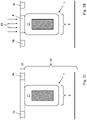
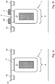
- Figure 1
- shows a portion of a semiconductor die with a transistor device in a sectional view;
- Figure 2a-h
- illustrate some process steps for manufacturing the transistor device of
figure 1 ; - Figure 3
- illustrates a further process step, which can be implemented optionally;
- Figure 4
- illustrates some variants of the transistor device, which can be integrated into the die, and an additional Schottky contact;
- Figure 5
- illustrates some manufacturing steps in a flow diagram.
-
Figure 1 illustrates atransistor device 1, which has asource region 2 and adrain region 3, the latter formed at a backside. Thesource region 2 is arranged at a frontside, together with abody region 4, in which a channel region 4.1 is formed. Agate region 5 with a gate electrode 5.1 and a gate dielectric 5.2 is formed above thebody region 4, thegate region 5 and the channel region 4.1 are oriented laterally. Between thebody region 4 and thedrain region 3, adrift region 6 is formed, wherein afield electrode trench 8 extends into thedrift region 6. In thetrench 8, afield electrode region 7 is formed, comprising a field electrode 7.1 and a field dielectric 7.2. - The
field electrode trench 8 with thefield electrode region 7 is formed in alower semiconductor body 30, which can be made of a substrate, in which thedrain region 3 is formed, and an epitaxial layer, in which thedrift region 6 is formed. On a frontside 30.1 of thelower semiconductor body 30, anupper epitaxial layer 35 is arranged. Thefield electrode trench 8 extends solely in thelower semiconductor body 30, it does not reach upwards into theupper epitaxial layer 35. The trench is covered by theupper epitaxial layer 35, and thesource region 2 andbody region 4, as well as thegate region 5, are formed vertically above thefield electrode trench 8. This allows for an efficient area use, as discussed in detail in the general description. - As apparent from the sectional view, the
source region 2 is arranged vertically above thefield electrode region 7, and asource contact 25 is formed centrally above the field electrode 7.1. It extends through an insulatinglayer 55, down to thesource region 2. In this example, it contacts also thebody region 4, namely extends into a highly dopedbody contact region 44. The latter is, like thebody region 4 in the example shown here, p-doped, but with a higher doping concentration. In the example shown here, thesource contact 25 ends on an insulatingspacer 27 formed in thefield electrode trench 8 above thefield electrode region 7. - Laterally opposite to the
source region 2, a dopedregion 70 is formed at the end of the channel region 4.1. It is of the same conductivity type as thesource region 2, n-type in the example shown here, and can for instance enable a channel performance optimization. - With the
source contact 25 arranged centrally, the channel region 4.1 and thegate region 5 extend in direction to a first side 8.1 of thefield electrode trench 8. On the other side of thesource contact 25, anadditional body region 40 with an additional channel region 40.1 and anadditional gate region 50 above are formed. They extend in direction to a second side 8.2 of thefield electrode trench 8, laterally opposite to the first side 8.1. With both channel regions 4.1, 40.1 arranged above thefield electrode trench 8, the area above can be used efficiently.Figure 2 a illustrates a process step, where thefield electrode trench 8 has already been etched into thelower epitaxial layer 30a formed on thesubstrate 30b. In the trench, thefield electrode region 7 has been formed, and the trench has been filled up with the insulatingspacer 27 above. - In a subsequent step shown in
figure 2b , stopislands 36 have been formed on thelower epitaxial layer 30a, namely on the frontside 30.1 of thelower semiconductor body 30. For that purpose, a stop layer, e. g. silicon nitride layer, is deposited and structured to arrive at the islands shown infigure 2b . Subsequently, theupper epitaxial layer 35 is deposited epitaxially, followed by a planarization, e. g. CMP. This results in the structure shown infigure 2c , thestop islands 36 lying flush in theupper epitaxial layer 35. -
Figures 2d ande illustrate animplantation 48 to form thebody region 4 and the formation of adielectric layer 45 for the gate dielectric, wherein the sequence of these process steps can also be inverse (layer formation prior to the implantation). Subsequently, thegate electrodes figure 2f . By a subsequent oxide or nitride deposition, combined with an etch back step,sidewall spacers 65 are formed at thegate electrodes dielectric layer 45 is etched back, and prevent an implantation at the edges during subsequent implantations, e. g. for the source region. - In
figure 2h , the insulatinglayer 55 has been deposited to cover thegate electrodes source contact 25. -
Figure 3 illustrates a process step that can be implemented optionally betweenfigures 2a and 2b . Here, an upper end 27.1 of the insulatingspacer 27 is recessed 39 into thefield electrode trench 8, namely arranged on a smaller vertical height than the frontside 30.1 of thelower semiconductor body 30. Likewise, a portion of thebody region 4 can be displaced into thefield electrode trench 8, see the general description in detail. -
Figure 4 illustratesdifferent transistor devices 1 integrated into the semiconductor die 20. In addition, between the twotransistor devices 1, aSchottky contact 60 extends through the insulatinglayer 55, it forms a Schottky diode 60.1 with thedrift region 6. The Schottky diode junction 60.1 can for instance decrease the forward voltage in diode conduction mode, see the general description in detail. TheSchottky contact 60 intersects thestop island 37, allowing for an efficient area use. - The
transistor device 1 shown on the right hand of theSchottky contact 60 is constructed as explained in detail with reference tofigure 1 . Thetransistor device 1 on the left hand of theSchottky contact 60 has basically the same set-up, differing only in the extension of thesource contact 25. It extends down through the insulatingspacer 27 and contacts the field electrode 7.1. Across thedie 20, the two types shown can vary, wherein the impendence in a switching application can be adapted by the frequency. - On the insulating
layer 55, afrontside metallization 70 is formed, e. g. an aluminum metallization, serving as a source metallization. Thefrontside metallization 70 above thecell field 71 is electrically isolated from a metallization shown on the right and serving as agate metallization 75. Viagate contacts 76 extending through the insulatinglayer 55, it is electrically connected to the gate electrodes 5.1, 50.1. -
Figure 5 illustrates some process steps 80 in a flow diagram. After etching 81 the field electrode trench, the field electrode region is formed 82. For forming 83 the body region, the upper epitaxial layer is deposited and doped. By forming 84 the gate region, the channel region is defined.
Claims (15)
- A semiconductor die (20) with a transistor device (1), havinga source and a drain region (2, 3),a body region (4) comprising a channel region (4.1),a gate region (5), which comprises a gate electrode (5.1), next to the channel region (4.1), for controlling a channel formation,a drift region (6) between the channel region (4.1) and the drain region (3), anda field electrode region (7) with a field electrode (7.1) formed in a field electrode trench (8), which extends into the drift region (6),wherein the channel region (4.1) extends laterally and is aligned vertically with the gate region (5),
and wherein at least a portion of the channel region (4.1) is arranged vertically above the field electrode region (7). - The semiconductor die (20) of claim 1, wherein the source region (2) is arranged vertically above the field electrode region (7).
- The semiconductor die (20) of claim 1 or 2, wherein a source contact (25, 26), which extends vertically into the source region (2), is arranged vertically above the field electrode (7.1).
- The semiconductor die (20) of claim 3, an insulating spacer (27) being formed vertically above the field electrode (7.1) in the field electrode trench (8), wherein the source contact (25) extends to the insulating spacer (27).
- The semiconductor die (20) of any of the preceding claims, an insulating spacer (27) being formed vertically above the field electrode (7.1) in the field electrode trench (6), wherein an upper end (27.1) of the insulating spacer (27) is recessed into the field electrode trench (6).
- The semiconductor die (20) of any one of the preceding claims, comprising an additional channel region (40.1) and an additional gate region (50), the additional channel region (40.1) extending laterally and being aligned vertically with the additional gate region (50), wherein at least a portion of the additional channel region (40.1) is arranged vertically above the field electrode region (7), and wherein, seen in a vertical cross-section, the channel regions (4.1, 40.1) extend towards opposite sides (8.1, 8.2) of the field electrode trench (8), respectively.
- The semiconductor die (20) of any one of the preceding claims, the field electrode trench (8) extending into a lower semiconductor body (30), wherein the body region (4) is formed in an upper epitaxial layer (35) provided on the lower semiconductor body (30).
- The semiconductor die (20) of claim 7, wherein the upper epitaxial layer (35) is, seen in a vertical cross section, interrupted by stop islands (36) lying flush in the upper epitaxial layer (35).
- The semiconductor die (20) of any one of the preceding claims, an insulating layer (55) covering the gate electrode (5.1), wherein a Schottky contact (60) extends through the insulating layer (55) and contacts the drift region (6).
- The semiconductor die (20) of claims 8 and 9, wherein the Schottky contact (60) extends through one of the stop islands (35).
- The semiconductor die (20) of any of the preceding claims, wherein the gate electrode (5.1) is formed on an upper epitaxial layer (35), a sidewall spacer (65) of an insulating material being formed between a sidewall of gate electrode and the epitaxial layer (35).
- The semiconductor die (20) of any one of the preceding claims, wherein a doped region (70) is formed at an end of the channel region (4.1) laterally opposite to the source region (2), the doped region (70) being of the same conductivity type as the source region (2).
- A method of manufacturing the semiconductor die (20) of any one of the preceding claims, comprising the steps:i) etching (81) the field electrode trench (8);ii) forming (82) the field electrode region (7) with the field electrode (7.1) in the field electrode trench (8);iii) forming (83) the body region (4);iv) forming (84) the gate region (5) next to the body region (4) to define the channel region (4.1).
- The method of claim 13 for manufacturing the die (20) of claim 7 or 8, optionally also in combination with any of claims 9 to 12, wherein step iii) is performed after steps i) and ii) and comprises the deposition of the epitaxial layer (35) onto the frontside (30.1) of the semiconductor body (30).
- The method of claim 14, wherein a gate dielectric (5.2) of the gate region (5) is formed by forming a dielectric layer (45) on the upper epitaxial layer (35).
Priority Applications (2)
| Application Number | Priority Date | Filing Date | Title |
|---|---|---|---|
| EP21175154.0A EP4092752A1 (en) | 2021-05-21 | 2021-05-21 | Semiconductor die with a transistor device and method of manufacturing the same |
| US17/743,523 US12389658B2 (en) | 2021-05-21 | 2022-05-13 | Semiconductor die with a transistor device and method of manufacturing the same |
Applications Claiming Priority (1)
| Application Number | Priority Date | Filing Date | Title |
|---|---|---|---|
| EP21175154.0A EP4092752A1 (en) | 2021-05-21 | 2021-05-21 | Semiconductor die with a transistor device and method of manufacturing the same |
Publications (1)
| Publication Number | Publication Date |
|---|---|
| EP4092752A1 true EP4092752A1 (en) | 2022-11-23 |
Family
ID=76059669
Family Applications (1)
| Application Number | Title | Priority Date | Filing Date |
|---|---|---|---|
| EP21175154.0A Withdrawn EP4092752A1 (en) | 2021-05-21 | 2021-05-21 | Semiconductor die with a transistor device and method of manufacturing the same |
Country Status (2)
| Country | Link |
|---|---|
| US (1) | US12389658B2 (en) |
| EP (1) | EP4092752A1 (en) |
Citations (5)
| Publication number | Priority date | Publication date | Assignee | Title |
|---|---|---|---|---|
| JP2000208757A (en) * | 1999-01-08 | 2000-07-28 | Nippon Telegr & Teleph Corp <Ntt> | Insulated gate type semiconductor device and manufacturing method thereof |
| US6362505B1 (en) * | 1998-11-27 | 2002-03-26 | Siemens Aktiengesellschaft | MOS field-effect transistor with auxiliary electrode |
| US20020175351A1 (en) * | 2001-04-11 | 2002-11-28 | Baliga Bantval Jayant | Power semiconductor devices having retrograded-doped transition regions that enhance breakdown voltage characteristics and methods of forming same |
| US20040007766A1 (en) * | 2002-07-09 | 2004-01-15 | Kabushiki Kaisha Toshiba | Semiconductor device and method for manufacturing the same |
| US20180226502A1 (en) * | 2017-02-08 | 2018-08-09 | Texas Instruments Incorporated | Power transistor with terminal trenches in terminal resurf regions |
Family Cites Families (1)
| Publication number | Priority date | Publication date | Assignee | Title |
|---|---|---|---|---|
| DE102015122938B4 (en) * | 2015-12-30 | 2021-11-11 | Infineon Technologies Austria Ag | TRANSISTOR WITH FIELD ELECTRODE AND METHOD FOR MANUFACTURING IT |
-
2021
- 2021-05-21 EP EP21175154.0A patent/EP4092752A1/en not_active Withdrawn
-
2022
- 2022-05-13 US US17/743,523 patent/US12389658B2/en active Active
Patent Citations (5)
| Publication number | Priority date | Publication date | Assignee | Title |
|---|---|---|---|---|
| US6362505B1 (en) * | 1998-11-27 | 2002-03-26 | Siemens Aktiengesellschaft | MOS field-effect transistor with auxiliary electrode |
| JP2000208757A (en) * | 1999-01-08 | 2000-07-28 | Nippon Telegr & Teleph Corp <Ntt> | Insulated gate type semiconductor device and manufacturing method thereof |
| US20020175351A1 (en) * | 2001-04-11 | 2002-11-28 | Baliga Bantval Jayant | Power semiconductor devices having retrograded-doped transition regions that enhance breakdown voltage characteristics and methods of forming same |
| US20040007766A1 (en) * | 2002-07-09 | 2004-01-15 | Kabushiki Kaisha Toshiba | Semiconductor device and method for manufacturing the same |
| US20180226502A1 (en) * | 2017-02-08 | 2018-08-09 | Texas Instruments Incorporated | Power transistor with terminal trenches in terminal resurf regions |
Also Published As
| Publication number | Publication date |
|---|---|
| US20220376063A1 (en) | 2022-11-24 |
| US12389658B2 (en) | 2025-08-12 |
Similar Documents
| Publication | Publication Date | Title |
|---|---|---|
| US11469313B2 (en) | Self-aligned trench MOSFET and IGBT structures and methods of fabrication | |
| US9502554B2 (en) | High frequency switching MOSFETs with low output capacitance using a depletable P-shield | |
| US9484453B2 (en) | Device structure and methods of making high density MOSFETs for load switch and DC-DC applications | |
| US9911840B2 (en) | Self aligned trench MOSFET with integrated diode | |
| US8723317B2 (en) | Trench metal oxide semiconductor field effect transistor with embedded schottky rectifier using reduced masks process | |
| US20240194754A1 (en) | Semiconductor device and corresponding methods of manufacture | |
| US20110121386A1 (en) | Trench MOSFET with trenched floating gates as termination | |
| US11699725B2 (en) | Semiconductor device having an alignment layer with mask pits | |
| WO2007002857A2 (en) | Structures and methods for forming shielded gate field effect transistors | |
| US20090315103A1 (en) | Trench mosfet with shallow trench for gate charge reduction | |
| US20090072306A1 (en) | Semiconductor device and method of manufacturing semiconductor device | |
| US20230087151A1 (en) | Field plate arrangement for trench gate fet | |
| US20100127324A1 (en) | Trench MOSFET with terrace gate and self-aligned source trench contact | |
| US20110008939A1 (en) | Method of making a trench MOSFET having improved avalanche capability using three masks process | |
| US20230268421A1 (en) | Method for auto-aligned manufacturing of a trench-gate mos transistor, and shielded-gate mos transistor | |
| US20020074578A1 (en) | Trench schottky barrier rectifier and method of making the same | |
| US20070063272A1 (en) | Semiconductor power device with insulated gate formed in a trench, and manufacturing process thereof | |
| US12389658B2 (en) | Semiconductor die with a transistor device and method of manufacturing the same | |
| US20240234518A9 (en) | Transistor device and method of fabricating contacts to a semiconductor substrate | |
| US9496357B2 (en) | Semiconductor device | |
| CN116741824A (en) | Semiconductor components and methods of forming the same | |
| CN117280456A (en) | Semiconductor die with vertical power transistor devices | |
| CN224178517U (en) | Super junction power semiconductor device | |
| EP4528820A1 (en) | Semiconductor device and method of manufacturing the same |
Legal Events
| Date | Code | Title | Description |
|---|---|---|---|
| PUAI | Public reference made under article 153(3) epc to a published international application that has entered the european phase |
Free format text: ORIGINAL CODE: 0009012 |
|
| STAA | Information on the status of an ep patent application or granted ep patent |
Free format text: STATUS: THE APPLICATION HAS BEEN PUBLISHED |
|
| AK | Designated contracting states |
Kind code of ref document: A1 Designated state(s): AL AT BE BG CH CY CZ DE DK EE ES FI FR GB GR HR HU IE IS IT LI LT LU LV MC MK MT NL NO PL PT RO RS SE SI SK SM TR |
|
| STAA | Information on the status of an ep patent application or granted ep patent |
Free format text: STATUS: REQUEST FOR EXAMINATION WAS MADE |
|
| 17P | Request for examination filed |
Effective date: 20230522 |
|
| RBV | Designated contracting states (corrected) |
Designated state(s): AL AT BE BG CH CY CZ DE DK EE ES FI FR GB GR HR HU IE IS IT LI LT LU LV MC MK MT NL NO PL PT RO RS SE SI SK SM TR |
|
| STAA | Information on the status of an ep patent application or granted ep patent |
Free format text: STATUS: EXAMINATION IS IN PROGRESS |
|
| 17Q | First examination report despatched |
Effective date: 20250227 |
|
| STAA | Information on the status of an ep patent application or granted ep patent |
Free format text: STATUS: THE APPLICATION IS DEEMED TO BE WITHDRAWN |
|
| 18D | Application deemed to be withdrawn |
Effective date: 20250628 |