EP4092740A1 - Semiconductor die with a vertical transistor device - Google Patents
Semiconductor die with a vertical transistor device Download PDFInfo
- Publication number
- EP4092740A1 EP4092740A1 EP21175157.3A EP21175157A EP4092740A1 EP 4092740 A1 EP4092740 A1 EP 4092740A1 EP 21175157 A EP21175157 A EP 21175157A EP 4092740 A1 EP4092740 A1 EP 4092740A1
- Authority
- EP
- European Patent Office
- Prior art keywords
- transistor device
- region
- pull
- capacitor
- trench
- Prior art date
- Legal status (The legal status is an assumption and is not a legal conclusion. Google has not performed a legal analysis and makes no representation as to the accuracy of the status listed.)
- Granted
Links
Images




Classifications
-
- H—ELECTRICITY
- H10—SEMICONDUCTOR DEVICES; ELECTRIC SOLID-STATE DEVICES NOT OTHERWISE PROVIDED FOR
- H10D—INORGANIC ELECTRIC SEMICONDUCTOR DEVICES
- H10D84/00—Integrated devices formed in or on semiconductor substrates that comprise only semiconducting layers, e.g. on Si wafers or on GaAs-on-Si wafers
- H10D84/101—Integrated devices comprising main components and built-in components, e.g. IGBT having built-in freewheel diode
- H10D84/141—VDMOS having built-in components
-
- H—ELECTRICITY
- H03—ELECTRONIC CIRCUITRY
- H03K—PULSE TECHNIQUE
- H03K17/00—Electronic switching or gating, i.e. not by contact-making and –breaking
- H03K17/16—Modifications for eliminating interference voltages or currents
- H03K17/161—Modifications for eliminating interference voltages or currents in field-effect transistor switches
- H03K17/165—Modifications for eliminating interference voltages or currents in field-effect transistor switches by feedback from the output circuit to the control circuit
-
- H—ELECTRICITY
- H10—SEMICONDUCTOR DEVICES; ELECTRIC SOLID-STATE DEVICES NOT OTHERWISE PROVIDED FOR
- H10D—INORGANIC ELECTRIC SEMICONDUCTOR DEVICES
- H10D1/00—Resistors, capacitors or inductors
- H10D1/40—Resistors
- H10D1/47—Resistors having no potential barriers
-
- H—ELECTRICITY
- H10—SEMICONDUCTOR DEVICES; ELECTRIC SOLID-STATE DEVICES NOT OTHERWISE PROVIDED FOR
- H10D—INORGANIC ELECTRIC SEMICONDUCTOR DEVICES
- H10D1/00—Resistors, capacitors or inductors
- H10D1/60—Capacitors
- H10D1/62—Capacitors having potential barriers
- H10D1/66—Conductor-insulator-semiconductor capacitors, e.g. MOS capacitors
- H10D1/665—Trench conductor-insulator-semiconductor capacitors, e.g. trench MOS capacitors
-
- H—ELECTRICITY
- H10—SEMICONDUCTOR DEVICES; ELECTRIC SOLID-STATE DEVICES NOT OTHERWISE PROVIDED FOR
- H10D—INORGANIC ELECTRIC SEMICONDUCTOR DEVICES
- H10D1/00—Resistors, capacitors or inductors
- H10D1/60—Capacitors
- H10D1/68—Capacitors having no potential barriers
- H10D1/692—Electrodes
-
- H—ELECTRICITY
- H10—SEMICONDUCTOR DEVICES; ELECTRIC SOLID-STATE DEVICES NOT OTHERWISE PROVIDED FOR
- H10D—INORGANIC ELECTRIC SEMICONDUCTOR DEVICES
- H10D30/00—Field-effect transistors [FET]
- H10D30/01—Manufacture or treatment
- H10D30/021—Manufacture or treatment of FETs having insulated gates [IGFET]
- H10D30/028—Manufacture or treatment of FETs having insulated gates [IGFET] of double-diffused metal oxide semiconductor [DMOS] FETs
- H10D30/0291—Manufacture or treatment of FETs having insulated gates [IGFET] of double-diffused metal oxide semiconductor [DMOS] FETs of vertical DMOS [VDMOS] FETs
-
- H—ELECTRICITY
- H10—SEMICONDUCTOR DEVICES; ELECTRIC SOLID-STATE DEVICES NOT OTHERWISE PROVIDED FOR
- H10D—INORGANIC ELECTRIC SEMICONDUCTOR DEVICES
- H10D30/00—Field-effect transistors [FET]
- H10D30/60—Insulated-gate field-effect transistors [IGFET]
- H10D30/64—Double-diffused metal-oxide semiconductor [DMOS] FETs
- H10D30/66—Vertical DMOS [VDMOS] FETs
-
- H—ELECTRICITY
- H10—SEMICONDUCTOR DEVICES; ELECTRIC SOLID-STATE DEVICES NOT OTHERWISE PROVIDED FOR
- H10D—INORGANIC ELECTRIC SEMICONDUCTOR DEVICES
- H10D62/00—Semiconductor bodies, or regions thereof, of devices having potential barriers
- H10D62/10—Shapes, relative sizes or dispositions of the regions of the semiconductor bodies; Shapes of the semiconductor bodies
- H10D62/13—Semiconductor regions connected to electrodes carrying current to be rectified, amplified or switched, e.g. source or drain regions
- H10D62/149—Source or drain regions of field-effect devices
- H10D62/151—Source or drain regions of field-effect devices of IGFETs
- H10D62/156—Drain regions of DMOS transistors
- H10D62/157—Impurity concentrations or distributions
-
- H—ELECTRICITY
- H10—SEMICONDUCTOR DEVICES; ELECTRIC SOLID-STATE DEVICES NOT OTHERWISE PROVIDED FOR
- H10D—INORGANIC ELECTRIC SEMICONDUCTOR DEVICES
- H10D62/00—Semiconductor bodies, or regions thereof, of devices having potential barriers
- H10D62/10—Shapes, relative sizes or dispositions of the regions of the semiconductor bodies; Shapes of the semiconductor bodies
- H10D62/17—Semiconductor regions connected to electrodes not carrying current to be rectified, amplified or switched, e.g. channel regions
- H10D62/351—Substrate regions of field-effect devices
- H10D62/357—Substrate regions of field-effect devices of FETs
- H10D62/364—Substrate regions of field-effect devices of FETs of IGFETs
- H10D62/371—Inactive supplementary semiconductor regions, e.g. for preventing punch-through, improving capacity effect or leakage current
-
- H—ELECTRICITY
- H10—SEMICONDUCTOR DEVICES; ELECTRIC SOLID-STATE DEVICES NOT OTHERWISE PROVIDED FOR
- H10D—INORGANIC ELECTRIC SEMICONDUCTOR DEVICES
- H10D62/00—Semiconductor bodies, or regions thereof, of devices having potential barriers
- H10D62/10—Shapes, relative sizes or dispositions of the regions of the semiconductor bodies; Shapes of the semiconductor bodies
- H10D62/17—Semiconductor regions connected to electrodes not carrying current to be rectified, amplified or switched, e.g. channel regions
- H10D62/351—Substrate regions of field-effect devices
- H10D62/357—Substrate regions of field-effect devices of FETs
- H10D62/364—Substrate regions of field-effect devices of FETs of IGFETs
- H10D62/378—Contact regions to the substrate regions
-
- H—ELECTRICITY
- H10—SEMICONDUCTOR DEVICES; ELECTRIC SOLID-STATE DEVICES NOT OTHERWISE PROVIDED FOR
- H10D—INORGANIC ELECTRIC SEMICONDUCTOR DEVICES
- H10D64/00—Electrodes of devices having potential barriers
- H10D64/111—Field plates
- H10D64/112—Field plates comprising multiple field plate segments
-
- H—ELECTRICITY
- H10—SEMICONDUCTOR DEVICES; ELECTRIC SOLID-STATE DEVICES NOT OTHERWISE PROVIDED FOR
- H10D—INORGANIC ELECTRIC SEMICONDUCTOR DEVICES
- H10D64/00—Electrodes of devices having potential barriers
- H10D64/111—Field plates
- H10D64/117—Recessed field plates, e.g. trench field plates or buried field plates
-
- H—ELECTRICITY
- H10—SEMICONDUCTOR DEVICES; ELECTRIC SOLID-STATE DEVICES NOT OTHERWISE PROVIDED FOR
- H10D—INORGANIC ELECTRIC SEMICONDUCTOR DEVICES
- H10D64/00—Electrodes of devices having potential barriers
- H10D64/20—Electrodes characterised by their shapes, relative sizes or dispositions
- H10D64/23—Electrodes carrying the current to be rectified, amplified, oscillated or switched, e.g. sources, drains, anodes or cathodes
- H10D64/251—Source or drain electrodes for field-effect devices
- H10D64/256—Source or drain electrodes for field-effect devices for lateral devices wherein the source or drain electrodes are recessed in semiconductor bodies
-
- H—ELECTRICITY
- H10—SEMICONDUCTOR DEVICES; ELECTRIC SOLID-STATE DEVICES NOT OTHERWISE PROVIDED FOR
- H10D—INORGANIC ELECTRIC SEMICONDUCTOR DEVICES
- H10D84/00—Integrated devices formed in or on semiconductor substrates that comprise only semiconducting layers, e.g. on Si wafers or on GaAs-on-Si wafers
- H10D84/80—Integrated devices formed in or on semiconductor substrates that comprise only semiconducting layers, e.g. on Si wafers or on GaAs-on-Si wafers characterised by the integration of at least one component covered by groups H10D12/00 or H10D30/00, e.g. integration of IGFETs
- H10D84/811—Combinations of field-effect devices and one or more diodes, capacitors or resistors
Definitions
- the present disclosure relates to a semiconductor die with a vertical power transistor device.
- the vertical power device has a source and a drain region at opposite sides of a semiconductor body. Via a gate electrode, a channel path formation in its body region and, in consequence, the current flow can be controlled.
- the die with the vertical power device can be co-packaged with other dies, e. g. with another power device and/or a driver chip.
- a DC-DC converter can for example comprise two discrete power transistors and the driver chip in a common package.
- the die comprises a pull-down transistor device, which is switchable between a conducting and a blocking state via a control terminal. It is connected between the gate electrode of the vertical device and a ground terminal and grounds the gate electrode of the vertical device in the conducting state.
- a capacitor is provided between its control terminal and a load terminal of the vertical device, namely either its source region or in particular its drain region.
- the potential at the respective load terminal rises and charges the capacitor.
- the control terminal of the pull-down device is also charged. It switches into the conducting state, pulling the gate potential of the vertical device to ground.
- This can for instance limit a capacitive charging of the gate electrode of the vertical device, which could for example result from a rising drain potential during the overshoot event.
- grounding the gate electrode e. g. gate oscillations of the power device can be minimized.
- the monolithic integration of the vertical and the pull-down device, together with the capacitor coupling these two devices, in the same die can enable a higher order integration, reducing for instance the complexity on package level.
- the integrated capacitor can be a self-controlling setup, triggered by an overshoot on the load terminal, e. g. drain region.
- the pull-down transistor is directly driven by the overshoot event, e. g. without an external control circuit, which can reduce the number of external connections or interfaces.
- an approach of this application is to combine a vertical power transistor device with a pull-down device and a trigger circuit connecting the control terminal of the pull-down device to the vertical device monolithically in the same die.
- Particular embodiments and features are presented throughout this disclosure and in the dependent claims. Thereby, the individual features shall be disclosed independently of a specific claim category, the disclosure relates to apparatus and device aspects, but also to method and use aspects. If for instance a device or die manufactured in a specific way is described, this is also a disclosure of a respective manufacturing process, and vice versa.
- Source and drain of the vertical device are arranged at opposite sides of the die, in particular the source region at the frontside and the drain region at the backside.
- Its channel region can extend vertically, namely be arranged laterally aside a gate region formed for example in a vertical gate trench.
- the channel can extend laterally and, in consequence, be aligned vertically with the gate region, see in detail below.
- Providing the vertical device with a lateral gate can for instance simplify the integration of the lateral device into the same die, e. g. allow for a certain process integration ("re-use" of one or more power device process steps for the pull-down device).
- load terminal is used to comprise both, the source and the drain region of the vertical power device.
- the capacitor is connected between the control terminal of the pull-down device and the drain region of the vertical device.
- the power device can be used in a so-called high side configuration, namely be connected between the supply voltage and the load, the pull-down device allowing for instance for a slightly increased switching speed or loss reduction (on the other hand, an avalanche of the vertical device could occur at lower currents, which could affect the long-term stability).
- the power device is used in a low side configuration, connected between load and ground, wherein the pull-down device can for instance minimize the gate oscillations, see above.
- a first resistor is formed in the die and connected between the capacitor and the control terminal of the pull-down device. E. g. in an overshoot event, the control terminal of the pull-down device is charged via the first resistor, for instance when the drain potential rises and charges the capacitor.
- the first resistor can for example be formed in a metallization layer arranged on a smaller vertical height than a frontside metallization of the vertical device, in the same metallization layer e. g. a gate redistribution or a gate liner or finger of the vertical device can be formed.
- the resistance can also be adjusted via polysilicon in a trench, for instance of the second capacitor trench electrode, see below.
- a second resistor is formed in the die and connected between the control terminal of the pull-down device and the ground terminal.
- the control terminal is grounded via the second resistor.
- the second resistor can be formed in the metallization layer and/or in particular via vertical interconnects, e. g. interconnects to the frontside metallization.
- the resistance can also be adjusted via polysilicon, e. g. gate polysilicon, arranged in a trench or hole.
- the power device can be a p-channel device having an n-doped body region.
- it is an n-channel device, the body region being p-doped and the source and the drain region being n-doped.
- the source region can in particular be connected to the ground terminal of the die, the capacitor being connected between the control terminal of the pull-down device and the drain region of the power device.
- the pull-down device electrically connects the gate electrode to the source region of the vertical device, when in the conducting state. Due to the low-side configuration, where source is on ground, the pull-down device grounds the gate electrode.
- this drain region is arranged at a backside of the die or semiconductor body and forms a first capacitor electrode of the capacitor.
- the drain region itself is part of the capacitor, an overshoot being picked up directly.
- the drain region can in particular extend over the whole backside of the die ("common drain backside”), see in detail below.
- the source regions of the vertical device and of the pull-down device are connected with each other via the frontside metallization of the vertical device.
- the frontside metallization can be made of copper or in particular aluminum, e. g. AlCu. It can basically cover the area of the die, in which the power device is formed. In addition, it can extend above an area where the pull-down device is formed, covering the latter for instance completely.
- the gate metallization layer mentioned above can be arranged on a smaller vertical height, e. g. extend at least partially below the frontside metallization, and it can have a smaller vertical thickness.
- the drain region of the pull-down device is connected to the gate electrode of the vertical device via a gate metallization layer.
- a gate pad of die e. g. a bond pad
- a gate runner can be formed in the gate metallization layer.
- the gate runner can, seen in a vertical top view, extend for instance laterally aside the vertical device, e. g. I-, L-or U-shaped aside or around the cell field.
- Using the gate metallization layer for the connection between the gate electrode of the vertical device and the pull-down device can allow for a "re-use" of existing layers, enabling for example a process integration.
- the pull-down device is a lateral device, having a source and a drain region formed at the frontside of the semiconductor body.
- a well region and/or a shielding field electrode region can be formed in the semiconductor body.
- at least two shielding field electrode regions can be formed in a respective trench, the well region extending laterally between the trenches.
- At least a portion of the lateral pull-down device can be arranged above the well region and/or the shielding field electrode region.
- the well and/or shielding field electrode regions can be arranged vertically between the lateral pull-down device and a common drain backside of the semiconductor die or body.
- the well region can be doped with an opposite conductivity type as the source and the drain region of the vertical device, e. g. be p-doped in case of an n-channel power device. It can in particular be electrically connected to the source region of the vertical device and reduce or compensate the backside potential, in particular common drain potential.
- the same applies for the shielding field electrode region which can be provided as an alternative or in particular in combination with the well region.
- the shielding field electrode or electrodes can be made of polysilicon or metal or both.
- a common drain backside can be advantageous in view of the manufacturing or packaging effort, also in view of a process integration, wherein the well or shielding field electrode region can allow for a safe and stable operation of the lateral pull-down device (e. g. without deep trenches for an electrical isolation between the devices).
- a second capacitor electrode connected to the control terminal of the pull-down device comprises a trench electrode formed in a capacitor trench extending into the semiconductor body.
- the electrode can for instance be made of polysilicon or metal or both.
- the capacitor trench can in particular extend into a lower semiconductor body, in particular into a lower epitaxial layer, in which for instance the drift region of the vertical device can be formed (in another area of the die).
- a capacitor dielectric can be formed in the capacitor trench, and the capacity can for instance be tuned via the capacitor electrode depth and/or width, and also via the dielectric properties.
- the capacitor trench electrode or electrodes can form the capacitor together with a backside of the die, in particular together with the drain region (see above).
- the capacitor trench can be arranged outside an area of the vertical device, e. g. laterally aside the pull-down device and/or the vertical device.
- a metal plate on the frontside could pick up the backside potential which can reach up to the frontside.
- the vertical power device comprises a field electrode region formed in a field electrode trench extending into the drift region.
- the field electrode region comprises a field electrode, e. g. made of polysilicon or metal or both, and a field dielectric separating the field electrode from the drift region.
- the field electrode trench can for instance have a longitudinal extension, a plurality trenches being for instance arranged as parallel stripes.
- the field electrode trench can be a needle trench, wherein needle-shaped and longitudinal trenches can also be combined across the die.
- the field electrode can for instance be connected to the source region, e. g. to the frontside metallization.
- the field electrode trench of the vertical device and the capacitor trench, and/or the field electrode trench of the vertical device and the shielding field electrode trench can in particular be etched simultaneously, allowing for an integration of process steps.
- the respective field dielectrics and/or electrodes can be formed simultaneously.
- the field electrode trench and the capacitor electrode trench can in particular have the same vertical depth, alternatively or in addition the shielding field electrode trench can be deeper than the field electrode trench.
- the capacitor electrode is contacted via a vertical interconnect intersecting an insulating layer formed on the frontside of semiconductor body.
- the vertical interconnect can be made of metal, e. g. tungsten.
- a plurality of trench electrodes can be provided, each formed in a respective capacitor trench and contacted by a respective vertical interconnect.
- a metallization layer formed on the insulating layer can connect the vertical interconnects and, in consequence, the capacitor trench electrodes with each other, in particular a gate metallization layer (see above).
- the vertical interconnects can form the first resistor, see above.
- a metallization plate can be formed above the capacity trenches, one or a plurality of gate fingers being for instance formed on one lateral side of the plate and extending above the pull-down device cell field, contacting the control electrode or electrodes of the pull-down device.
- the semiconductor body comprises a lower semiconductor body and an upper epitaxial layer deposited onto the lower semiconductor body.
- the trenches e. g. field electrode and/or capacitor and/or shielding field electrode trenches
- the trenches are etched into the lower semiconductor body.
- the trenches solely extend in the lower semiconductor body, the upper epitaxial layer being for instance deposited after the trench etch and fill.
- the lower semiconductor body can for instance comprise a semiconductor substrate, e. g. silicon substrate, and a lower epitaxial layer deposited onto the substrate, wherein the trenches can particularly be formed solely in the lower epitaxial layer.
- the lateral device In the upper epitaxial layer, e. g. above the shielding field electrode trench and the well region, the lateral device can be formed.
- the source, body and drain region of the lateral device can be formed by respective implantations in the upper epitaxial layer.
- the lateral gate region can be formed subsequently on the upper epitaxial layer, e. g. by depositing and structuring a field dielectric layer and depositing and structuring a field electrode layer.
- the vertical power device comprises a lateral channel and gate region, wherein the former can in particular be formed in the upper epitaxial layer. Due to the lateral design, the gate and the channel region are vertically aligned, in particular the gate region above the channel region. Particularly, at least a portion of the lateral channel and gate region can be arranged above a field electrode region of the vertical device, seen in a vertical cross-section e. g. a portion of at least 30%, 50%, 70% or 90%, in particular the whole channel region can be vertically aligned with the field electrode region.
- the vertical device can in particular comprise a first gate region formed above a first side of the field electrode region or trench, and it can comprise a second gate region formed above a second side thereof, the first side lying at a first sidewall and the second side lying at a laterally opposite second sidewall of the field electrode trench of the vertical device, seen in a vertical cross-section.
- the lateral channel and gate region of the vertical device can allow for an efficient area use.
- a vertical channel which can be an alternative in general, the possibilities for a further lateral shrink can be limited, e. g. because the field electrode trench itself requires a certain lateral width.
- This limitation can be circumvented at least to some extent by arranging the channel region of the vertical power device above the field electrode trench.
- Providing not only the lateral but also the vertical transistor device with a lateral gate region can also allow for a certain process integration, e. g. a simultaneous formation of the gate dielectrics and/or the gate electrodes of the vertical and the lateral device.
- the application relates also to a method of manufacturing a semiconductor die disclosed here. It can comprise the steps:
- the first and/or second resistor can be formed in addition.
- Step iii) can in particular comprise a plurality of sub steps, e. g. the drain formation at the backside (first capacitor electrode) and the capacitor trench and trench electrode formation (second capacitor electrode).
- the field electrode and/or shielding field electrode trenches can be etched and/or filled simultaneously.
- Steps i) and ii) can also comprise simultaneous sub steps, e. g. a gate dielectric and/or gate electrode formation in case of the vertical power device with the lateral channel.
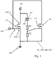
- the circuit diagram of figure 1 illustrates a vertical power device 2 having two load terminals 140, one being its source region 3 and the other one its drain region 4.
- the drain region 4 is connected to a load 141 and the source region 3 is connected to a ground terminal 150.
- a gate electrode 5.1 of the power device 2 is controllable via a gate terminal 185.
- a pull-down transistor device 20 and a capacitor C are formed.
- the latter comprises a first capacitor electrode 161 connected to a load terminal 140 of the vertical power device 2, namely to the drain region 4 in this example.
- a second capacitor electrode 162 is connected to a control terminal 145 of the pull-down device 20.
- the capacitor C is charged.
- the control terminal 145 of the pull-down device is charged as well, switching the pull-down device 20 into the conducting state. It consequently connects the gate electrode 5.1 of the vertical power device 2 to the ground terminal 150, which can for instance limit gate oscillations (the connection is indicated by the reference numerals 26, 170/300, 125, see fig. 3 and 5 for comparison).
- the control terminal 145 of the pull-down device 20 is discharged via a second resistor R 2 , it is grounded in steady-state operation. Consequently, the pull-down device 20 is switched to the blocking state again, and the gate electrode 5.1 of the vertical power device 2 is no longer grounded.
- Figure 2 shows a sectional view of a semiconductor die 1, into which the vertical power transistor device 2 and the pull-down transistor device 20 are integrated.
- the vertical power device 2 has a source region 3 formed at a frontside 10a and a drain region 4 formed at a backside 10b of a semiconductor body 10. Though being a vertical device with the source and the drain region 3, 4 at opposite sides 10a, b, a channel region 104.1 formed in a body region 104 of the vertical power device 2 extends laterally. For an efficient area use, it is arranged vertically above a field electrode region 5 formed in a field electrode trench 6. The latter extends into a drift region 9 and comprises a field electrode 7 and a field dielectric 8.
- an insulating layer 55 is arranged, e. g. a silicon oxide layer. It is intersected by a contact 125 of the vertical device 2, which is arranged vertically above the field electrode 7. The contact 125 electrically connects the source region 3 to a frontside metallization (not shown).
- a gate region 105 is arranged, it comprises a gate electrode 105.1 and a gate dielectric 105.2.
- the pull-down device 20 is formed in the die 1, namely as a lateral device. It has a body region 21 with a lateral channel region 21.1, as well as a source and a drain region 23, 24, see fig. 3 in detail. Due to the lateral design, the source and the drain region 23, 24 are both arranged at the frontside 10a of the semiconductor body 10. They are formed in an upper epitaxial layer 10.3, in which also the source region 3 and body region 104 of the vertical device 2 are arranged.
- a shielding field electrode region 30 with a shielding field electrode 31 is formed in a shielding field electrode trench 32.
- the shielding field electrode or electrodes 31 shield the pull-down device 20 with respect to the backside 10b, namely with respect to the backside drain potential, which can enable a common drain backside.
- the shielding field electrodes 31 can be contacted outside the sectional plane shown, e. g. outside the cell of the pull-down device (see fig. 6 ).
- a well region 35 is arranged, which is electrically connected to the vertical power FET source, see in detail figure 2 .
- an additional implant region 36 can be formed below the well region 35 to optimize the breakdown voltage.
- the shielding field electrode trenches 32 have a larger lateral width than the field electrode trenches 6 of the vertical device2. In consequence, since these trenches 6, 32 are in particular etched simultaneously, the shielding field electrode trenches 32 extend deeper into the semiconductor body 10, in particular the lower epitaxial layer 10.2.
- a bridge implant region 11 is formed below its field electrode trenches 6, namely between the drift region 9 and the drain region 4. It is of the same conductivity type as the drift region 9, n-type in this example, but has a higher doping concentration.
- Figure 3 illustrates the pull-down device 20 in a detailed view.
- a lateral gate region 44 is arranged above the body region 21 with the channel region 21.1, formed between the source and drain region 23, 24, a lateral gate region 44 is arranged. It comprises a lateral gate electrode 45 and a lateral gate dielectric 46.
- the gate region 44 is covered by the insulating layer 55, on which a metallization layer 180 is shown partly with dashed lines.
- an additional insulating layer 255 is arranged, on which a frontside metallization 170 is formed.
- the frontside metallization 170 forms a source plate (see below). In the area of the lateral device, it is connected to the source region 23 of the pull-down device 20 via a source contact 26.
- the latter intersects the insulating layers 55, 255, the source region 23 being consequently connected to the source region 3 of the vertical device 2, as illustrated in figure 1 .
- the source contact 26 contacts the well region 35 via a vertical implant region 49, the well region 35 being connected to the power device source in consequence.
- the pull-down device 20 is an n-channel device, the source and the drain region 23, 24 being n-doped, and the body region 21 being p-doped.
- the vertical implant region 49 and the well region 35 are also p-doped.
- the drain region 24 is connected via a drain contact 27, which extends through the insulating layer 55.
- the drain contact 27 is contacted via a drain metallization 320 formed in the metallization layer 180 and connected to the gate electrode 5.1 of the vertical device outside the drawing plane, see fig. 5 .
- the gate electrode 45 of the pull-down device 20, forming its control terminal 145, is connected to the second capacitor electrode 162, namely is coupled to the drain region 4 of the vertical device 2 via the resistor R 1 and the capacitor C.
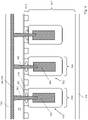
- FIG. 4 illustrates the capacitor, namely the first and the second capacitor electrode 161, 162.
- the first capacitor electrode 161 is formed by the drain region 4, which extends over the whole backside of the die (common drain backside).
- the second capacitor electrode 162 comprises trench electrodes 165 formed in a capacitor trench 166 respectively.
- the capacitor trenches 166 are etched into the lower epitaxial layer 10.2, the upper epitaxial layer 10.3 is formed subsequently above.
- the lower epitaxial layer 10.2 can for instance be doped as in the region of the power device, e. g. like the drift region.
- the trench electrodes 165 are connected to the metallization layer 180.
- a wiring to the gate electrode 45 of the pull-down device 20 is realised (which is different from the drain metallization 320 realised in the same metallization layer 180).
- the common drain backside is charged, which is picked up by the trench electrodes 165, such that the pull-down device 20 is switched into the conducting state and grounds the gate of the power device.
- the interconnects 182 are connected to embedded regions 198 of the same conductivity type like the body region 104, p-type in the example here, and connected to the latter.
- the interconnect 182 could extend through an isolator.
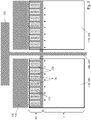
- Figure 5 illustrates the wiring and connection between the devices 2, 20 in a top view.
- two source plates 300 are formed in the layer of the frontside metallization 170.
- a gate runner 305 extends, which is formed in the metallization layer 180. All structures shown cross-hatched are formed in the same layer, the source plates 300 lying above and separated via the second insulating layer 255 (not shown here).
- the capacitor metallization 310 is formed above the capacitor trenches 166 (see fig. 4 ), via fingers 315 it contacts the gate electrode or electrodes 45 of the lateral devices 20.
- the small rectangles below the pull-down device 20 indicate field electrode contacts 330, which connect the shielding field electrodes to the frontside metallization 180, namely to source potential.
- the required timing for the charging and discharging of the control terminal 145 of the pull-down device 20 can be adjusted.
- the resistance of R 1 can for instance be influenced by the capacitor metallization 310 and the fingers 315, and also via the vertical interconnects 182 and the resistance of the trench electrode 165 shown in figure 4 .
- the second resistor R 2 can for instance be adjusted via vertical trenches or holes extending through the additional insulating layer 255 and connecting the capacitor metallization 310 and/or the fingers 315 to the frontside metallization 170, the trenches or holes being for instance filled with polysilicon to achieve a required resistance (which will depend on the application and the capacity and can for instance lie in a range of 10 - 200 ⁇ ).
- the source contact 26 is shown (not cross-hatched, with horizontal stripes), connecting the source region 23 to the source plate 300.
- the drain metallization 320 of the pull-down device 20 is shown, connecting the pull-down device 20 to the gate runner 305.
- the pull-down device 20 When the pull-down device 20 is in the conducting state, it connects the gate runner 305, namely the gate of the vertical device, to the source plate 300, namely to ground potential.
- a gate pad 325 is shown additionally.
- Figure 6 illustrates a section through the field electrode contacts 330 shown in figure 4 . They extend through the first and the second insulating layer 55, 255, connecting the shielding field electrodes 31 to the frontside metallization 180, namely to source potential. Together with the well regions 35, which are contacted inside the cell field of the pull-down device 20 (see figure 4 or 5 ), they shield the lateral device from the backside potential of the drain region 4. Via highly doped contact regions 197, the field electrode contacts 330 are connected to embedded regions 198 (p-type in the example here) and in consequence to the well regions 35.
- Figures 7a-d illustrate some manufacturing steps that can apply for both, the vertical and the lateral device.
- the respective trench 6, 32 has been etched into the lower epitaxial layer 10.2, and the respective field electrode region 5, 30 has been formed.
- the upper epitaxial layer 10.3 is deposited, covering the respective trench 6, 32, see figure 7b .
- a dielectric layer 85 is deposited ( figure 7c ), followed by a deposition of an electrically conductive layer 90.
- the gate electrode or electrodes can be defined.
- the dielectric layer 85 defines the gate dielectric, it can be removed from other locations of the die in an etch back step after the gate electrode formation. Implantations forming the different regions in the upper epitaxial layer 10.3 can be performed in between steps 7b and c and/or after the gate electrode formation.
- the upper epitaxial layer 10.3 can be doped in situ or in particular after its deposition to form the regions required for the respective device.
- Figure 8 shows a flow diagram and summarizes some process steps.
- the manufacturing comprises forming 400 the vertical power device 2 and forming 401 the pull-down transistor device 20, wherein at least some sub steps can be performed simultaneously.
- the manufacturing comprises forming 402 the capacity C , wherein the first capacitor electrode 161 can in particular be formed simultaneously with the drain region 4 of the vertical device 2 and/or the second capacitor electrode 162 can be formed simultaneously with field electrodes 7 of the vertical device 2 or the shielding field electrodes 31 below the pull-down device 20.
Landscapes
- Semiconductor Integrated Circuits (AREA)
- Metal-Oxide And Bipolar Metal-Oxide Semiconductor Integrated Circuits (AREA)
Abstract
Description
- The present disclosure relates to a semiconductor die with a vertical power transistor device.
- The vertical power device has a source and a drain region at opposite sides of a semiconductor body. Via a gate electrode, a channel path formation in its body region and, in consequence, the current flow can be controlled. Depending on the specific application, the die with the vertical power device can be co-packaged with other dies, e. g. with another power device and/or a driver chip. A DC-DC converter can for example comprise two discrete power transistors and the driver chip in a common package.
- It is an object of the present application to provide an improved semiconductor die with a vertical power device as well as a method of manufacturing the same.
- This object is achieved by the semiconductor die of
claim 1. Moreover, it is achieved by the method of claim 15. In addition to the vertical power device, the die comprises a pull-down transistor device, which is switchable between a conducting and a blocking state via a control terminal. It is connected between the gate electrode of the vertical device and a ground terminal and grounds the gate electrode of the vertical device in the conducting state. To trigger or switch the pull-down transistor into the conducting state, a capacitor is provided between its control terminal and a load terminal of the vertical device, namely either its source region or in particular its drain region. - During a switching event of the vertical device, the potential at the respective load terminal rises and charges the capacitor. In consequence, e. g. in an overshoot event, the control terminal of the pull-down device is also charged. It switches into the conducting state, pulling the gate potential of the vertical device to ground. This can for instance limit a capacitive charging of the gate electrode of the vertical device, which could for example result from a rising drain potential during the overshoot event. By grounding the gate electrode, e. g. gate oscillations of the power device can be minimized.
- The monolithic integration of the vertical and the pull-down device, together with the capacitor coupling these two devices, in the same die can enable a higher order integration, reducing for instance the complexity on package level. E. g. in comparison to an external driver for the pull-down device, the integrated capacitor can be a self-controlling setup, triggered by an overshoot on the load terminal, e. g. drain region. In other words, the pull-down transistor is directly driven by the overshoot event, e. g. without an external control circuit, which can reduce the number of external connections or interfaces.
- In general words, an approach of this application is to combine a vertical power transistor device with a pull-down device and a trigger circuit connecting the control terminal of the pull-down device to the vertical device monolithically in the same die. Particular embodiments and features are presented throughout this disclosure and in the dependent claims. Thereby, the individual features shall be disclosed independently of a specific claim category, the disclosure relates to apparatus and device aspects, but also to method and use aspects. If for instance a device or die manufactured in a specific way is described, this is also a disclosure of a respective manufacturing process, and vice versa.
- Source and drain of the vertical device are arranged at opposite sides of the die, in particular the source region at the frontside and the drain region at the backside. Its channel region can extend vertically, namely be arranged laterally aside a gate region formed for example in a vertical gate trench. In particular, however, the channel can extend laterally and, in consequence, be aligned vertically with the gate region, see in detail below. Providing the vertical device with a lateral gate can for instance simplify the integration of the lateral device into the same die, e. g. allow for a certain process integration ("re-use" of one or more power device process steps for the pull-down device).
- The more generic term "load terminal" is used to comprise both, the source and the drain region of the vertical power device. In particular, however, the capacitor is connected between the control terminal of the pull-down device and the drain region of the vertical device. In general, the power device can be used in a so-called high side configuration, namely be connected between the supply voltage and the load, the pull-down device allowing for instance for a slightly increased switching speed or loss reduction (on the other hand, an avalanche of the vertical device could occur at lower currents, which could affect the long-term stability). In particular, the power device is used in a low side configuration, connected between load and ground, wherein the pull-down device can for instance minimize the gate oscillations, see above.
- In an embodiment, a first resistor is formed in the die and connected between the capacitor and the control terminal of the pull-down device. E. g. in an overshoot event, the control terminal of the pull-down device is charged via the first resistor, for instance when the drain potential rises and charges the capacitor. The first resistor can for example be formed in a metallization layer arranged on a smaller vertical height than a frontside metallization of the vertical device, in the same metallization layer e. g. a gate redistribution or a gate liner or finger of the vertical device can be formed. The resistance can also be adjusted via polysilicon in a trench, for instance of the second capacitor trench electrode, see below.
- In an embodiment, a second resistor is formed in the die and connected between the control terminal of the pull-down device and the ground terminal. During normal operation, the control terminal is grounded via the second resistor. E. g. during an overshoot, it gets charged and the pull-down device is switched into the conducting state, before the control terminal reverts back to ground when the charge floats off via the second resistor. Like the first resistor, the second resistor can be formed in the metallization layer and/or in particular via vertical interconnects, e. g. interconnects to the frontside metallization. The resistance can also be adjusted via polysilicon, e. g. gate polysilicon, arranged in a trench or hole.
- In general, the power device can be a p-channel device having an n-doped body region. In a particular embodiment, it is an n-channel device, the body region being p-doped and the source and the drain region being n-doped. The source region can in particular be connected to the ground terminal of the die, the capacitor being connected between the control terminal of the pull-down device and the drain region of the power device. In other words, the pull-down device electrically connects the gate electrode to the source region of the vertical device, when in the conducting state. Due to the low-side configuration, where source is on ground, the pull-down device grounds the gate electrode.
- In an embodiment relating to the capacitor connected to the drain region of the power device, this drain region is arranged at a backside of the die or semiconductor body and forms a first capacitor electrode of the capacitor. In other words, the drain region itself is part of the capacitor, an overshoot being picked up directly. The drain region can in particular extend over the whole backside of the die ("common drain backside"), see in detail below.
- In an embodiment relating to the capacitor connected to the drain region, the source regions of the vertical device and of the pull-down device are connected with each other via the frontside metallization of the vertical device. The frontside metallization can be made of copper or in particular aluminum, e. g. AlCu. It can basically cover the area of the die, in which the power device is formed. In addition, it can extend above an area where the pull-down device is formed, covering the latter for instance completely. The gate metallization layer mentioned above can be arranged on a smaller vertical height, e. g. extend at least partially below the frontside metallization, and it can have a smaller vertical thickness.
- In an embodiment, the drain region of the pull-down device is connected to the gate electrode of the vertical device via a gate metallization layer. For the vertical power device, a gate pad of die, e. g. a bond pad, and/or a gate runner can be formed in the gate metallization layer. The gate runner can, seen in a vertical top view, extend for instance laterally aside the vertical device, e. g. I-, L-or U-shaped aside or around the cell field. Using the gate metallization layer for the connection between the gate electrode of the vertical device and the pull-down device can allow for a "re-use" of existing layers, enabling for example a process integration.
- In an embodiment, the pull-down device is a lateral device, having a source and a drain region formed at the frontside of the semiconductor body. Below the pull-down device, a well region and/or a shielding field electrode region can be formed in the semiconductor body. In particular, seen in a vertical cross-section, at least two shielding field electrode regions can be formed in a respective trench, the well region extending laterally between the trenches. At least a portion of the lateral pull-down device can be arranged above the well region and/or the shielding field electrode region. The well and/or shielding field electrode regions can be arranged vertically between the lateral pull-down device and a common drain backside of the semiconductor die or body.
- The well region can be doped with an opposite conductivity type as the source and the drain region of the vertical device, e. g. be p-doped in case of an n-channel power device. It can in particular be electrically connected to the source region of the vertical device and reduce or compensate the backside potential, in particular common drain potential. The same applies for the shielding field electrode region, which can be provided as an alternative or in particular in combination with the well region. The shielding field electrode or electrodes can be made of polysilicon or metal or both. A common drain backside can be advantageous in view of the manufacturing or packaging effort, also in view of a process integration, wherein the well or shielding field electrode region can allow for a safe and stable operation of the lateral pull-down device (e. g. without deep trenches for an electrical isolation between the devices).
- In an embodiment, a second capacitor electrode connected to the control terminal of the pull-down device comprises a trench electrode formed in a capacitor trench extending into the semiconductor body. The electrode can for instance be made of polysilicon or metal or both. The capacitor trench can in particular extend into a lower semiconductor body, in particular into a lower epitaxial layer, in which for instance the drift region of the vertical device can be formed (in another area of the die). In addition to the capacitor electrode, e. g. a capacitor dielectric can be formed in the capacitor trench, and the capacity can for instance be tuned via the capacitor electrode depth and/or width, and also via the dielectric properties. The capacitor trench electrode or electrodes can form the capacitor together with a backside of the die, in particular together with the drain region (see above). In case of a common drain backside, the capacitor trench can be arranged outside an area of the vertical device, e. g. laterally aside the pull-down device and/or the vertical device. In general, e. g. as an alternative to the capacitor trench electrodes, a metal plate on the frontside could pick up the backside potential which can reach up to the frontside.
- In an embodiment, the vertical power device comprises a field electrode region formed in a field electrode trench extending into the drift region. The field electrode region comprises a field electrode, e. g. made of polysilicon or metal or both, and a field dielectric separating the field electrode from the drift region. Seen in a vertical top view, the field electrode trench can for instance have a longitudinal extension, a plurality trenches being for instance arranged as parallel stripes. Alternatively, the field electrode trench can be a needle trench, wherein needle-shaped and longitudinal trenches can also be combined across the die. Depending on the application, the field electrode can for instance be connected to the source region, e. g. to the frontside metallization.
- The field electrode trench of the vertical device and the capacitor trench, and/or the field electrode trench of the vertical device and the shielding field electrode trench, can in particular be etched simultaneously, allowing for an integration of process steps. Alternatively or in addition, the respective field dielectrics and/or electrodes can be formed simultaneously. The field electrode trench and the capacitor electrode trench can in particular have the same vertical depth, alternatively or in addition the shielding field electrode trench can be deeper than the field electrode trench.
- In an embodiment, the capacitor electrode is contacted via a vertical interconnect intersecting an insulating layer formed on the frontside of semiconductor body. The vertical interconnect can be made of metal, e. g. tungsten. In particular, a plurality of trench electrodes can be provided, each formed in a respective capacitor trench and contacted by a respective vertical interconnect. A metallization layer formed on the insulating layer can connect the vertical interconnects and, in consequence, the capacitor trench electrodes with each other, in particular a gate metallization layer (see above). The vertical interconnects can form the first resistor, see above. Seen in a vertical top view, a metallization plate can be formed above the capacity trenches, one or a plurality of gate fingers being for instance formed on one lateral side of the plate and extending above the pull-down device cell field, contacting the control electrode or electrodes of the pull-down device.
- In an embodiment, the semiconductor body comprises a lower semiconductor body and an upper epitaxial layer deposited onto the lower semiconductor body. Therein, the trenches, e. g. field electrode and/or capacitor and/or shielding field electrode trenches, are etched into the lower semiconductor body. In particular, the trenches solely extend in the lower semiconductor body, the upper epitaxial layer being for instance deposited after the trench etch and fill. The lower semiconductor body can for instance comprise a semiconductor substrate, e. g. silicon substrate, and a lower epitaxial layer deposited onto the substrate, wherein the trenches can particularly be formed solely in the lower epitaxial layer.
- In the upper epitaxial layer, e. g. above the shielding field electrode trench and the well region, the lateral device can be formed. In particular, the source, body and drain region of the lateral device can be formed by respective implantations in the upper epitaxial layer. The lateral gate region can be formed subsequently on the upper epitaxial layer, e. g. by depositing and structuring a field dielectric layer and depositing and structuring a field electrode layer.
- In an embodiment, the vertical power device comprises a lateral channel and gate region, wherein the former can in particular be formed in the upper epitaxial layer. Due to the lateral design, the gate and the channel region are vertically aligned, in particular the gate region above the channel region. Particularly, at least a portion of the lateral channel and gate region can be arranged above a field electrode region of the vertical device, seen in a vertical cross-section e. g. a portion of at least 30%, 50%, 70% or 90%, in particular the whole channel region can be vertically aligned with the field electrode region. As illustrated in the exemplary embodiments in detail, the vertical device can in particular comprise a first gate region formed above a first side of the field electrode region or trench, and it can comprise a second gate region formed above a second side thereof, the first side lying at a first sidewall and the second side lying at a laterally opposite second sidewall of the field electrode trench of the vertical device, seen in a vertical cross-section.
- Generally, the lateral channel and gate region of the vertical device, and in particular the at least proportional arrangement above the field electrode trench, can allow for an efficient area use. With a vertical channel, which can be an alternative in general, the possibilities for a further lateral shrink can be limited, e. g. because the field electrode trench itself requires a certain lateral width. This limitation can be circumvented at least to some extent by arranging the channel region of the vertical power device above the field electrode trench. Providing not only the lateral but also the vertical transistor device with a lateral gate region can also allow for a certain process integration, e. g. a simultaneous formation of the gate dielectrics and/or the gate electrodes of the vertical and the lateral device.
- As mentioned, the application relates also to a method of manufacturing a semiconductor die disclosed here. It can comprise the steps:
- i) forming the vertical power device;
- ii) forming the pull-down transistor device;
- iii) forming the capacitor C.
- Regarding further possible process details, reference is made to the description above and to the exemplary embodiments. For instance, the first and/or second resistor can be formed in addition. Step iii) can in particular comprise a plurality of sub steps, e. g. the drain formation at the backside (first capacitor electrode) and the capacitor trench and trench electrode formation (second capacitor electrode). Thereby, the field electrode and/or shielding field electrode trenches can be etched and/or filled simultaneously. Steps i) and ii) can also comprise simultaneous sub steps, e. g. a gate dielectric and/or gate electrode formation in case of the vertical power device with the lateral channel.
- Below, the semiconductor die with the vertical and the pull-down devices and the manufacturing are explained in further detail by means of exemplary embodiments. Therein, the individual features can also be relevant in a different combination.
- Figure 1
- shows a circuit diagram illustrating the coupling of a vertical power device and a pull-down device;
- Figure 2
- shows a vertical cross-section and illustrates the integration of the vertical power device and the pull-down device into the same die;
- Figure 3
- illustrates the pull-device in a detailed view;
- Figure 4
- shows a capacitor coupling the vertical device to the pull-down device;
- Figure 5
- illustrates the wiring between the capacitor of
figure 4 and the pull-down device offigure 3 , as well as between the vertical and the pull-down devices, in a top view; - Figure 6
- illustrates a contacting of shielding field electrodes arranged below the pull-down device;
- Figures 7a-d
- illustrate some manufacturing steps;
- Figure 8
- summarizes some manufacturing steps in a flow diagram.
- The circuit diagram of
figure 1 illustrates avertical power device 2 having two load terminals 140, one being itssource region 3 and the other one itsdrain region 4. In the low side configuration shown, thedrain region 4 is connected to aload 141 and thesource region 3 is connected to aground terminal 150. A gate electrode 5.1 of thepower device 2 is controllable via agate terminal 185. - Integrated in the same die with the
power device 2, a pull-down transistor device 20 and a capacitor C are formed. The latter comprises afirst capacitor electrode 161 connected to a load terminal 140 of thevertical power device 2, namely to thedrain region 4 in this example. Asecond capacitor electrode 162 is connected to acontrol terminal 145 of the pull-down device 20. In case of an overshoot event, namely an increasing potential at thedrain region 4, the capacitor C is charged. In consequence, thecontrol terminal 145 of the pull-down device is charged as well, switching the pull-down device 20 into the conducting state. It consequently connects the gate electrode 5.1 of thevertical power device 2 to theground terminal 150, which can for instance limit gate oscillations (the connection is indicated by thereference numerals fig. 3 and5 for comparison). - The
control terminal 145 of the pull-down device 20 is discharged via a second resistor R2, it is grounded in steady-state operation. Consequently, the pull-down device 20 is switched to the blocking state again, and the gate electrode 5.1 of thevertical power device 2 is no longer grounded. -
Figure 2 shows a sectional view of asemiconductor die 1, into which the verticalpower transistor device 2 and the pull-down transistor device 20 are integrated. Thevertical power device 2 has asource region 3 formed at a frontside 10a and adrain region 4 formed at abackside 10b of asemiconductor body 10. Though being a vertical device with the source and thedrain region opposite sides 10a, b, a channel region 104.1 formed in abody region 104 of thevertical power device 2 extends laterally. For an efficient area use, it is arranged vertically above afield electrode region 5 formed in afield electrode trench 6. The latter extends into adrift region 9 and comprises afield electrode 7 and afield dielectric 8. - On the frontside 10a of the
semiconductor body 10, an insulatinglayer 55 is arranged, e. g. a silicon oxide layer. It is intersected by acontact 125 of thevertical device 2, which is arranged vertically above thefield electrode 7. Thecontact 125 electrically connects thesource region 3 to a frontside metallization (not shown). On the frontside 10a, covered by the insulatinglayer 55, agate region 105 is arranged, it comprises a gate electrode 105.1 and a gate dielectric 105.2. - In addition to the
vertical device 2, the pull-down device 20 is formed in thedie 1, namely as a lateral device. It has abody region 21 with a lateral channel region 21.1, as well as a source and adrain region fig. 3 in detail. Due to the lateral design, the source and thedrain region semiconductor body 10. They are formed in an upper epitaxial layer 10.3, in which also thesource region 3 andbody region 104 of thevertical device 2 are arranged. - Below the pull-
down device 20, in a lower semiconductor body 10.1, 10.2, in particular in a lower epitaxial layer 10.2, a shieldingfield electrode region 30 with a shieldingfield electrode 31 is formed in a shieldingfield electrode trench 32. The shielding field electrode orelectrodes 31 shield the pull-down device 20 with respect to thebackside 10b, namely with respect to the backside drain potential, which can enable a common drain backside. The shieldingfield electrodes 31 can be contacted outside the sectional plane shown, e. g. outside the cell of the pull-down device (seefig. 6 ). Between the shieldingfield electrode trenches 32, awell region 35 is arranged, which is electrically connected to the vertical power FET source, see in detailfigure 2 . In addition, anadditional implant region 36 can be formed below thewell region 35 to optimize the breakdown voltage. - The shielding
field electrode trenches 32 have a larger lateral width than thefield electrode trenches 6 of the vertical device2. In consequence, since thesetrenches field electrode trenches 32 extend deeper into thesemiconductor body 10, in particular the lower epitaxial layer 10.2. To shorten a vertical current path in thedrift region 9 of thevertical device 2, abridge implant region 11 is formed below itsfield electrode trenches 6, namely between thedrift region 9 and thedrain region 4. It is of the same conductivity type as thedrift region 9, n-type in this example, but has a higher doping concentration. -
Figure 3 illustrates the pull-down device 20 in a detailed view. Above thebody region 21 with the channel region 21.1, formed between the source and drainregion lateral gate region 44 is arranged. It comprises alateral gate electrode 45 and alateral gate dielectric 46. Thegate region 44 is covered by the insulatinglayer 55, on which ametallization layer 180 is shown partly with dashed lines. On themetallization layer 180, an additional insulatinglayer 255 is arranged, on which afrontside metallization 170 is formed. Above thevertical power device 2, thefrontside metallization 170 forms a source plate (see below). In the area of the lateral device, it is connected to thesource region 23 of the pull-down device 20 via asource contact 26. The latter intersects the insulatinglayers source region 23 being consequently connected to thesource region 3 of thevertical device 2, as illustrated infigure 1 . - In addition, the
source contact 26 contacts thewell region 35 via avertical implant region 49, thewell region 35 being connected to the power device source in consequence. In the example shown, the pull-down device 20 is an n-channel device, the source and thedrain region body region 21 being p-doped. Thevertical implant region 49 and thewell region 35 are also p-doped. - The
drain region 24 is connected via adrain contact 27, which extends through the insulatinglayer 55. Thedrain contact 27 is contacted via adrain metallization 320 formed in themetallization layer 180 and connected to the gate electrode 5.1 of the vertical device outside the drawing plane, seefig. 5 . Thegate electrode 45 of the pull-down device 20, forming itscontrol terminal 145, is connected to thesecond capacitor electrode 162, namely is coupled to thedrain region 4 of thevertical device 2 via the resistor R1 and the capacitor C. -
Figure 4 illustrates the capacitor, namely the first and thesecond capacitor electrode first capacitor electrode 161 is formed by thedrain region 4, which extends over the whole backside of the die (common drain backside). Thesecond capacitor electrode 162 comprisestrench electrodes 165 formed in acapacitor trench 166 respectively. Thecapacitor trenches 166 are etched into the lower epitaxial layer 10.2, the upper epitaxial layer 10.3 is formed subsequently above. In this region of the die, the lower epitaxial layer 10.2 can for instance be doped as in the region of the power device, e. g. like the drift region. Viavertical interconnects 182 extending through the insulatinglayer 55, thetrench electrodes 165 are connected to themetallization layer 180. There, a wiring to thegate electrode 45 of the pull-down device 20 is realised (which is different from thedrain metallization 320 realised in the same metallization layer 180). In case of an overshoot event, the common drain backside is charged, which is picked up by thetrench electrodes 165, such that the pull-down device 20 is switched into the conducting state and grounds the gate of the power device. Via highlydoped contact regions 197, theinterconnects 182 are connected to embeddedregions 198 of the same conductivity type like thebody region 104, p-type in the example here, and connected to the latter. Alternatively, theinterconnect 182 could extend through an isolator. -
Figure 5 illustrates the wiring and connection between thedevices frontside metallization 170, two source plates 300 are formed. Laterally in between, but at a smaller vertical height, a gate runner 305 extends, which is formed in themetallization layer 180. All structures shown cross-hatched are formed in the same layer, the source plates 300 lying above and separated via the second insulating layer 255 (not shown here). Thecapacitor metallization 310 is formed above the capacitor trenches 166 (seefig. 4 ), viafingers 315 it contacts the gate electrode orelectrodes 45 of thelateral devices 20. - The small rectangles below the pull-
down device 20 indicatefield electrode contacts 330, which connect the shielding field electrodes to thefrontside metallization 180, namely to source potential. Via the first and the second resistor R1 and R2 shown infigure 1 , e. g. the required timing for the charging and discharging of thecontrol terminal 145 of the pull-down device 20 can be adjusted. The resistance of R1 can for instance be influenced by thecapacitor metallization 310 and thefingers 315, and also via thevertical interconnects 182 and the resistance of thetrench electrode 165 shown infigure 4 . The second resistor R2 can for instance be adjusted via vertical trenches or holes extending through the additional insulatinglayer 255 and connecting thecapacitor metallization 310 and/or thefingers 315 to thefrontside metallization 170, the trenches or holes being for instance filled with polysilicon to achieve a required resistance (which will depend on the application and the capacity and can for instance lie in a range of 10 - 200 Ω). - Laterally in between, respectively, the
source contact 26 is shown (not cross-hatched, with horizontal stripes), connecting thesource region 23 to the source plate 300. Moreover, thedrain metallization 320 of the pull-down device 20 is shown, connecting the pull-down device 20 to the gate runner 305. When the pull-down device 20 is in the conducting state, it connects the gate runner 305, namely the gate of the vertical device, to the source plate 300, namely to ground potential. For the purpose of illustration, agate pad 325 is shown additionally. -
Figure 6 illustrates a section through thefield electrode contacts 330 shown infigure 4 . They extend through the first and the second insulatinglayer field electrodes 31 to thefrontside metallization 180, namely to source potential. Together with thewell regions 35, which are contacted inside the cell field of the pull-down device 20 (seefigure 4 or5 ), they shield the lateral device from the backside potential of thedrain region 4. Via highlydoped contact regions 197, thefield electrode contacts 330 are connected to embedded regions 198 (p-type in the example here) and in consequence to thewell regions 35. -
Figures 7a-d illustrate some manufacturing steps that can apply for both, the vertical and the lateral device. Infigure 7a , therespective trench field electrode region respective trench figure 7b . Subsequently, adielectric layer 85 is deposited (figure 7c ), followed by a deposition of an electricallyconductive layer 90. By structuring the latter, e. g. prior to the deposition by a mask or in a subsequent etch back step, the gate electrode or electrodes can be defined. Thedielectric layer 85 defines the gate dielectric, it can be removed from other locations of the die in an etch back step after the gate electrode formation. Implantations forming the different regions in the upper epitaxial layer 10.3 can be performed in between steps 7b and c and/or after the gate electrode formation. The upper epitaxial layer 10.3 can be doped in situ or in particular after its deposition to form the regions required for the respective device. -
Figure 8 shows a flow diagram and summarizes some process steps. the manufacturing comprises forming 400 thevertical power device 2 and forming 401 the pull-down transistor device 20, wherein at least some sub steps can be performed simultaneously. Moreover, the manufacturing comprises forming 402 the capacity C, wherein thefirst capacitor electrode 161 can in particular be formed simultaneously with thedrain region 4 of thevertical device 2 and/or thesecond capacitor electrode 162 can be formed simultaneously withfield electrodes 7 of thevertical device 2 or the shieldingfield electrodes 31 below the pull-down device 20.
Claims (15)
- A semiconductor die (1), comprisinga vertical power transistor device (2),
the vertical power transistor device (2) having a source region (3) and a drain region (4) at opposite sides (10.a, 10.b) of a semiconductor body (10), forming a load terminal (140) respectively, and a gate electrode (5.1);a pull-down transistor device (20),
the pull-down transistor device (20) having a control terminal (145) and switchable between a conducting state and a blocking state via the control terminal (145), anda capacitor (C),wherein the pull-down transistor device (20) is connected between the gate electrode (5.1) of the vertical power transistor device (2) and a ground terminal (150) and connects the gate electrode (5.1) to the ground terminal (150) in the conducting state, and wherein the capacitor (C) is connected between one of the load terminals (140) of the vertical power transistor device (2) and the control terminal (145) of the pull-down transistor device (20) and capacitively couples the one load terminal (140) to the control terminal (145). - The semiconductor die (1) of claim 1, a first resistor (R1 ) formed in the die (1) and connected between the capacitor (C) and the control terminal (145) of the pull-down transistor device (20).
- The semiconductor die (1) of claim 1 or 2, a second resistor (R 2) formed in the die (1) and connected between the control terminal (145) of the pull-down transistor device (20) and the ground terminal (150).
- The semiconductor die (1) of any one of the preceding claims, the vertical power transistor device (2) being an n-channel device and the capacitor (C) being connected to its drain region (4), wherein the source region (3) of the vertical power transistor device (2) is connected to the ground terminal (150).
- The semiconductor die (1) of any one of the preceding claims, the capacitor (C) being connected to the drain region (4) of the vertical power transistor device (2), the drain region (4) arranged at a backside (10b) of the semiconductor body (10) and forming a first capacitor electrode (161) of the capacitor (C).
- The semiconductor die (1) of any one of the preceding claims, wherein the source region (3) of the vertical power transistor device (2) and a source region (23) of the pull-down transistor device (20) are electrically connected via a frontside metallization layer (170) of the vertical power transistor device (2) formed on a frontside (10a) of the semiconductor body (10), the frontside metallization layer (170) extending above the pull-down transistor device (20).
- The semiconductor die (1) of any one of the preceding claims, wherein a drain region (24) of the pull-down transistor device (20) and the gate electrode (5.1) of the vertical power transistor device (2) are electrically connected in a metallization layer (180), in which a gate pad (325) of the die (1) and/or a gate runner (305) laterally aside the vertical power transistor device (2) are formed.
- The semiconductor die (1) of any one of the preceding claims, the pull-down transistor device (20) having a body region (21) with a lateral channel region (21.1), as well as a source and a drain region (23, 24) formed at a frontside (10a) of the semiconductor body (10), wherein a well region (35) is formed in the semiconductor body (10), the well region (35) doped with an opposite conductivity type as the source and the drain region (3, 4) of the vertical power transistor device (2), and wherein at least a portion of the pull-down transistor device (20) is arranged vertically above the well region (35).
- The semiconductor die (1) of any one of the preceding claims, the pull-down transistor device (20) having a body region (21) with a lateral channel region (21.1), as well as a source and a drain region (23, 24) formed at a frontside (10a) of the semiconductor body (10), wherein a shielding field electrode region (30) with a shielding field electrode (31) is formed in a shielding field electrode trench (32) in the semiconductor body (10), and wherein at least a portion of the pull-down transistor device (20) is arranged vertically above the shielding field electrode region (30).
- The semiconductor die (1) of any one of the preceding claims, wherein a second capacitor electrode (162) of the capacitor (C), which is connected to the control terminal (145) of the pull-down transistor device (20), comprises a trench electrode (165) formed in a capacitor trench (166) in the semiconductor body (10).
- The semiconductor die (1) of claim 10, the vertical power transistor device (2) comprising a field electrode region (7) formed in a field electrode trench (8) in a drift region (6), the field electrode trench (8) and the capacitor electrode trench (166) having in particular the same depth.
- The semiconductor die (1) of claim 10 or 11, the second capacitor electrode (162) comprising a plurality trench electrodes (165), each formed in a respective capacitor trench (166) in the semiconductor body (10), wherein a metallization layer (180) is formed on a frontside (10a) of the semiconductor body (10) above an insulating layer (55), the metallization layer (180) connected to the trench electrodes (165) via vertical interconnects (182).
- The semiconductor die (1) of any one of claims 9 to 12, the semiconductor body (10) comprising a lower semiconductor body (10.1, 10.2) and an upper epitaxial layer (10.3) deposited onto the lower semiconductor body (10.1, 10.2), wherein the shielding field electrode trench (32) and/or the capacitor trench (166) and/or the field electrode trench (8) extend from a frontside (10a) of the lower semiconductor body (10.1, 10.2) into the latter.
- The semiconductor die (1) of any one of the preceding claims, the semiconductor body (10) comprising a lower semiconductor body (10.1, 10.2) and an upper epitaxial layer (10.3) deposited onto the lower semiconductor body (10.1, 10.2), wherein the source region (3) and a channel region (4.1) of the vertical power transistor device (2) are formed in the upper epitaxial layer (10.3).
- A method of manufacturing the semiconductor die (1) of any one of the preceding claims, comprising the steps:i) forming (400) the vertical power device (2);ii) forming (401) the pull-down transistor device (20);iii) forming (402) the capacitor (C).
Priority Applications (4)
| Application Number | Priority Date | Filing Date | Title |
|---|---|---|---|
| EP21175157.3A EP4092740B1 (en) | 2021-05-21 | 2021-05-21 | Semiconductor die with a vertical transistor device |
| US17/743,535 US12433013B2 (en) | 2021-05-21 | 2022-05-13 | Semiconductor die with a vertical transistor device |
| KR1020220060516A KR20220157897A (en) | 2021-05-21 | 2022-05-18 | Semiconductor die with a vertical transistor device |
| CN202210548468.9A CN115377096A (en) | 2021-05-21 | 2022-05-20 | Semiconductor die with vertical transistor devices |
Applications Claiming Priority (1)
| Application Number | Priority Date | Filing Date | Title |
|---|---|---|---|
| EP21175157.3A EP4092740B1 (en) | 2021-05-21 | 2021-05-21 | Semiconductor die with a vertical transistor device |
Publications (2)
| Publication Number | Publication Date |
|---|---|
| EP4092740A1 true EP4092740A1 (en) | 2022-11-23 |
| EP4092740B1 EP4092740B1 (en) | 2025-06-25 |
Family
ID=76076213
Family Applications (1)
| Application Number | Title | Priority Date | Filing Date |
|---|---|---|---|
| EP21175157.3A Active EP4092740B1 (en) | 2021-05-21 | 2021-05-21 | Semiconductor die with a vertical transistor device |
Country Status (4)
| Country | Link |
|---|---|
| US (1) | US12433013B2 (en) |
| EP (1) | EP4092740B1 (en) |
| KR (1) | KR20220157897A (en) |
| CN (1) | CN115377096A (en) |
Citations (6)
| Publication number | Priority date | Publication date | Assignee | Title |
|---|---|---|---|---|
| EP0703664A2 (en) * | 1994-09-20 | 1996-03-27 | Hitachi, Ltd. | Semiconductor circuit comprising means for malfunction prevention, and its use, particularly for inverters |
| US6545316B1 (en) * | 2000-06-23 | 2003-04-08 | Silicon Wireless Corporation | MOSFET devices having linear transfer characteristics when operating in velocity saturation mode and methods of forming and operating same |
| US20060126253A1 (en) * | 2004-12-14 | 2006-06-15 | Mitsubishi Denki Kabushiki Kaisha | Inverter circuit |
| US20110148376A1 (en) * | 2009-12-23 | 2011-06-23 | Texas Instruments Incorporated | Mosfet with gate pull-down |
| US20140084295A1 (en) * | 2012-09-21 | 2014-03-27 | Infineon Technologies Austria Ag | Transistor Device with Field Electrode |
| US20140264577A1 (en) * | 2013-03-15 | 2014-09-18 | Infineon Technologies Austria Ag | Adjustable Transistor Device |
Family Cites Families (6)
| Publication number | Priority date | Publication date | Assignee | Title |
|---|---|---|---|---|
| KR102055658B1 (en) * | 2013-06-18 | 2019-12-16 | 온세미컨덕터코리아 주식회사 | Gate driver, swtcih control circuit and power supply device comprsing the gate driver circuit |
| US20160240640A1 (en) * | 2014-01-14 | 2016-08-18 | Mitsubishi Electric Corporation | Power semiconductor device |
| EP3249815B1 (en) * | 2016-05-23 | 2019-08-28 | NXP USA, Inc. | Circuit arrangement for fast turn-off of bi-directional switching device |
| US10601314B2 (en) * | 2017-09-08 | 2020-03-24 | Infineon Technologies Austria Ag | Power semiconductor systems having inductor modules, and methods of manufacturing inductor modules and power semiconductor systems having inductor modules |
| JP7318335B2 (en) * | 2019-06-14 | 2023-08-01 | 富士電機株式会社 | integrated circuits, semiconductor devices |
| US11428750B1 (en) * | 2019-12-12 | 2022-08-30 | Smart Wires Inc. | Monitoring non-uniform capacitor and IGBT degradation with current sensors |
-
2021
- 2021-05-21 EP EP21175157.3A patent/EP4092740B1/en active Active
-
2022
- 2022-05-13 US US17/743,535 patent/US12433013B2/en active Active
- 2022-05-18 KR KR1020220060516A patent/KR20220157897A/en not_active Ceased
- 2022-05-20 CN CN202210548468.9A patent/CN115377096A/en active Pending
Patent Citations (6)
| Publication number | Priority date | Publication date | Assignee | Title |
|---|---|---|---|---|
| EP0703664A2 (en) * | 1994-09-20 | 1996-03-27 | Hitachi, Ltd. | Semiconductor circuit comprising means for malfunction prevention, and its use, particularly for inverters |
| US6545316B1 (en) * | 2000-06-23 | 2003-04-08 | Silicon Wireless Corporation | MOSFET devices having linear transfer characteristics when operating in velocity saturation mode and methods of forming and operating same |
| US20060126253A1 (en) * | 2004-12-14 | 2006-06-15 | Mitsubishi Denki Kabushiki Kaisha | Inverter circuit |
| US20110148376A1 (en) * | 2009-12-23 | 2011-06-23 | Texas Instruments Incorporated | Mosfet with gate pull-down |
| US20140084295A1 (en) * | 2012-09-21 | 2014-03-27 | Infineon Technologies Austria Ag | Transistor Device with Field Electrode |
| US20140264577A1 (en) * | 2013-03-15 | 2014-09-18 | Infineon Technologies Austria Ag | Adjustable Transistor Device |
Also Published As
| Publication number | Publication date |
|---|---|
| US20220375929A1 (en) | 2022-11-24 |
| KR20220157897A (en) | 2022-11-29 |
| US12433013B2 (en) | 2025-09-30 |
| CN115377096A (en) | 2022-11-22 |
| EP4092740B1 (en) | 2025-06-25 |
Similar Documents
| Publication | Publication Date | Title |
|---|---|---|
| US11031390B2 (en) | Bidirectional switch having back to back field effect transistors | |
| US8552585B2 (en) | MOS transistor device in common source configuration | |
| TWI744851B (en) | Bidirectional power device and manufacturing method thereof | |
| US10388781B2 (en) | Device structure having inter-digitated back to back MOSFETs | |
| TWI634620B (en) | Power device integration on a common substrate | |
| US6891223B2 (en) | Transistor configuration with a structure for making electrical contact with electrodes of a trench transistor cell | |
| TWI443836B (en) | Power device integration on a common substrate | |
| TWI747226B (en) | Bidirectional power device and manufacturing method thereof | |
| TWI623083B (en) | Power device integration on a common substrate | |
| US9368621B1 (en) | Power semiconductor device having low on-state resistance | |
| CN112309976B (en) | Bidirectional power device manufacturing method | |
| US8258555B2 (en) | Semiconductor device having extra capacitor structure | |
| US20070138544A1 (en) | Field plate trench transistor and method for producing it | |
| TW202034527A (en) | Bidirectional power device | |
| US9899343B2 (en) | High voltage tolerant bonding pad structure for trench-based semiconductor devices | |
| EP4092740B1 (en) | Semiconductor die with a vertical transistor device | |
| EP4092724A1 (en) | Semiconductor die with a vertical power transistor device | |
| EP4432359A1 (en) | Semiconductor die with a vertical device | |
| US20250255009A1 (en) | Semiconductor circuit with a semiconductor device | |
| CN113192885B (en) | Bidirectional power devices and their manufacturing methods | |
| CN213660381U (en) | Bidirectional power device |
Legal Events
| Date | Code | Title | Description |
|---|---|---|---|
| PUAI | Public reference made under article 153(3) epc to a published international application that has entered the european phase |
Free format text: ORIGINAL CODE: 0009012 |
|
| STAA | Information on the status of an ep patent application or granted ep patent |
Free format text: STATUS: THE APPLICATION HAS BEEN PUBLISHED |
|
| AK | Designated contracting states |
Kind code of ref document: A1 Designated state(s): AL AT BE BG CH CY CZ DE DK EE ES FI FR GB GR HR HU IE IS IT LI LT LU LV MC MK MT NL NO PL PT RO RS SE SI SK SM TR |
|
| STAA | Information on the status of an ep patent application or granted ep patent |
Free format text: STATUS: REQUEST FOR EXAMINATION WAS MADE |
|
| 17P | Request for examination filed |
Effective date: 20230509 |
|
| RBV | Designated contracting states (corrected) |
Designated state(s): AL AT BE BG CH CY CZ DE DK EE ES FI FR GB GR HR HU IE IS IT LI LT LU LV MC MK MT NL NO PL PT RO RS SE SI SK SM TR |
|
| REG | Reference to a national code |
Ref country code: DE Ref legal event code: R079 Free format text: PREVIOUS MAIN CLASS: H01L0027060000 Ipc: H10D0030010000 Ref country code: DE Ref legal event code: R079 Ref document number: 602021032705 Country of ref document: DE Free format text: PREVIOUS MAIN CLASS: H01L0027060000 Ipc: H10D0030010000 |
|
| GRAP | Despatch of communication of intention to grant a patent |
Free format text: ORIGINAL CODE: EPIDOSNIGR1 |
|
| STAA | Information on the status of an ep patent application or granted ep patent |
Free format text: STATUS: GRANT OF PATENT IS INTENDED |
|
| RIC1 | Information provided on ipc code assigned before grant |
Ipc: H10D 62/17 20250101ALI20250212BHEP Ipc: H10D 30/66 20250101ALI20250212BHEP Ipc: H10D 1/66 20250101ALI20250212BHEP Ipc: H10D 84/80 20250101ALI20250212BHEP Ipc: H10D 84/00 20250101ALI20250212BHEP Ipc: H03K 17/16 20060101ALI20250212BHEP Ipc: H10D 64/23 20250101ALI20250212BHEP Ipc: H10D 64/20 20250101ALI20250212BHEP Ipc: H10D 62/13 20250101ALI20250212BHEP Ipc: H10D 30/01 20250101AFI20250212BHEP |
|
| INTG | Intention to grant announced |
Effective date: 20250224 |
|
| GRAS | Grant fee paid |
Free format text: ORIGINAL CODE: EPIDOSNIGR3 |
|
| GRAA | (expected) grant |
Free format text: ORIGINAL CODE: 0009210 |
|
| STAA | Information on the status of an ep patent application or granted ep patent |
Free format text: STATUS: THE PATENT HAS BEEN GRANTED |
|
| P01 | Opt-out of the competence of the unified patent court (upc) registered |
Free format text: CASE NUMBER: APP_20472/2025 Effective date: 20250429 |
|
| AK | Designated contracting states |
Kind code of ref document: B1 Designated state(s): AL AT BE BG CH CY CZ DE DK EE ES FI FR GB GR HR HU IE IS IT LI LT LU LV MC MK MT NL NO PL PT RO RS SE SI SK SM TR |
|
| REG | Reference to a national code |
Ref country code: GB Ref legal event code: FG4D |
|
| REG | Reference to a national code |
Ref country code: CH Ref legal event code: EP |
|
| REG | Reference to a national code |
Ref country code: DE Ref legal event code: R096 Ref document number: 602021032705 Country of ref document: DE |
|
| REG | Reference to a national code |
Ref country code: CH Ref legal event code: EP |
|
| REG | Reference to a national code |
Ref country code: IE Ref legal event code: FG4D |
|
| PG25 | Lapsed in a contracting state [announced via postgrant information from national office to epo] |
Ref country code: FI Free format text: LAPSE BECAUSE OF FAILURE TO SUBMIT A TRANSLATION OF THE DESCRIPTION OR TO PAY THE FEE WITHIN THE PRESCRIBED TIME-LIMIT Effective date: 20250625 |
|
| REG | Reference to a national code |
Ref country code: LT Ref legal event code: MG9D |
|
| PG25 | Lapsed in a contracting state [announced via postgrant information from national office to epo] |
Ref country code: NO Free format text: LAPSE BECAUSE OF FAILURE TO SUBMIT A TRANSLATION OF THE DESCRIPTION OR TO PAY THE FEE WITHIN THE PRESCRIBED TIME-LIMIT Effective date: 20250925 Ref country code: GR Free format text: LAPSE BECAUSE OF FAILURE TO SUBMIT A TRANSLATION OF THE DESCRIPTION OR TO PAY THE FEE WITHIN THE PRESCRIBED TIME-LIMIT Effective date: 20250926 |
|
| PG25 | Lapsed in a contracting state [announced via postgrant information from national office to epo] |
Ref country code: BG Free format text: LAPSE BECAUSE OF FAILURE TO SUBMIT A TRANSLATION OF THE DESCRIPTION OR TO PAY THE FEE WITHIN THE PRESCRIBED TIME-LIMIT Effective date: 20250625 |
|
| PG25 | Lapsed in a contracting state [announced via postgrant information from national office to epo] |
Ref country code: HR Free format text: LAPSE BECAUSE OF FAILURE TO SUBMIT A TRANSLATION OF THE DESCRIPTION OR TO PAY THE FEE WITHIN THE PRESCRIBED TIME-LIMIT Effective date: 20250625 |
|
| PG25 | Lapsed in a contracting state [announced via postgrant information from national office to epo] |
Ref country code: RS Free format text: LAPSE BECAUSE OF FAILURE TO SUBMIT A TRANSLATION OF THE DESCRIPTION OR TO PAY THE FEE WITHIN THE PRESCRIBED TIME-LIMIT Effective date: 20250925 |
|
| PG25 | Lapsed in a contracting state [announced via postgrant information from national office to epo] |
Ref country code: LV Free format text: LAPSE BECAUSE OF FAILURE TO SUBMIT A TRANSLATION OF THE DESCRIPTION OR TO PAY THE FEE WITHIN THE PRESCRIBED TIME-LIMIT Effective date: 20250625 |
|
| REG | Reference to a national code |
Ref country code: NL Ref legal event code: MP Effective date: 20250625 |
|
| PG25 | Lapsed in a contracting state [announced via postgrant information from national office to epo] |
Ref country code: NL Free format text: LAPSE BECAUSE OF FAILURE TO SUBMIT A TRANSLATION OF THE DESCRIPTION OR TO PAY THE FEE WITHIN THE PRESCRIBED TIME-LIMIT Effective date: 20250625 |
|
| PG25 | Lapsed in a contracting state [announced via postgrant information from national office to epo] |
Ref country code: PT Free format text: LAPSE BECAUSE OF FAILURE TO SUBMIT A TRANSLATION OF THE DESCRIPTION OR TO PAY THE FEE WITHIN THE PRESCRIBED TIME-LIMIT Effective date: 20251027 |
|
| REG | Reference to a national code |
Ref country code: AT Ref legal event code: MK05 Ref document number: 1808066 Country of ref document: AT Kind code of ref document: T Effective date: 20250625 |
|
| PG25 | Lapsed in a contracting state [announced via postgrant information from national office to epo] |
Ref country code: IS Free format text: LAPSE BECAUSE OF FAILURE TO SUBMIT A TRANSLATION OF THE DESCRIPTION OR TO PAY THE FEE WITHIN THE PRESCRIBED TIME-LIMIT Effective date: 20251025 |
|
| PG25 | Lapsed in a contracting state [announced via postgrant information from national office to epo] |
Ref country code: AT Free format text: LAPSE BECAUSE OF FAILURE TO SUBMIT A TRANSLATION OF THE DESCRIPTION OR TO PAY THE FEE WITHIN THE PRESCRIBED TIME-LIMIT Effective date: 20250625 Ref country code: SM Free format text: LAPSE BECAUSE OF FAILURE TO SUBMIT A TRANSLATION OF THE DESCRIPTION OR TO PAY THE FEE WITHIN THE PRESCRIBED TIME-LIMIT Effective date: 20250625 |
|
| PG25 | Lapsed in a contracting state [announced via postgrant information from national office to epo] |
Ref country code: CZ Free format text: LAPSE BECAUSE OF FAILURE TO SUBMIT A TRANSLATION OF THE DESCRIPTION OR TO PAY THE FEE WITHIN THE PRESCRIBED TIME-LIMIT Effective date: 20250625 |
|
| PG25 | Lapsed in a contracting state [announced via postgrant information from national office to epo] |
Ref country code: PL Free format text: LAPSE BECAUSE OF FAILURE TO SUBMIT A TRANSLATION OF THE DESCRIPTION OR TO PAY THE FEE WITHIN THE PRESCRIBED TIME-LIMIT Effective date: 20250625 |
|
| PG25 | Lapsed in a contracting state [announced via postgrant information from national office to epo] |
Ref country code: EE Free format text: LAPSE BECAUSE OF FAILURE TO SUBMIT A TRANSLATION OF THE DESCRIPTION OR TO PAY THE FEE WITHIN THE PRESCRIBED TIME-LIMIT Effective date: 20250625 |
|
| PG25 | Lapsed in a contracting state [announced via postgrant information from national office to epo] |
Ref country code: SK Free format text: LAPSE BECAUSE OF FAILURE TO SUBMIT A TRANSLATION OF THE DESCRIPTION OR TO PAY THE FEE WITHIN THE PRESCRIBED TIME-LIMIT Effective date: 20250625 |
|
| PG25 | Lapsed in a contracting state [announced via postgrant information from national office to epo] |
Ref country code: ES Free format text: LAPSE BECAUSE OF FAILURE TO SUBMIT A TRANSLATION OF THE DESCRIPTION OR TO PAY THE FEE WITHIN THE PRESCRIBED TIME-LIMIT Effective date: 20250625 |
|
| REG | Reference to a national code |
Ref country code: DE Ref legal event code: R097 Ref document number: 602021032705 Country of ref document: DE |
|
| PG25 | Lapsed in a contracting state [announced via postgrant information from national office to epo] |
Ref country code: DK Free format text: LAPSE BECAUSE OF FAILURE TO SUBMIT A TRANSLATION OF THE DESCRIPTION OR TO PAY THE FEE WITHIN THE PRESCRIBED TIME-LIMIT Effective date: 20250625 |
|
| PG25 | Lapsed in a contracting state [announced via postgrant information from national office to epo] |
Ref country code: IT Free format text: LAPSE BECAUSE OF FAILURE TO SUBMIT A TRANSLATION OF THE DESCRIPTION OR TO PAY THE FEE WITHIN THE PRESCRIBED TIME-LIMIT Effective date: 20250625 |
|
| PLBE | No opposition filed within time limit |
Free format text: ORIGINAL CODE: 0009261 |
|
| STAA | Information on the status of an ep patent application or granted ep patent |
Free format text: STATUS: NO OPPOSITION FILED WITHIN TIME LIMIT |
|
| REG | Reference to a national code |
Ref country code: CH Ref legal event code: L10 Free format text: ST27 STATUS EVENT CODE: U-0-0-L10-L00 (AS PROVIDED BY THE NATIONAL OFFICE) Effective date: 20260507 |
|
| 26N | No opposition filed |
Effective date: 20260326 |
|
| PG25 | Lapsed in a contracting state [announced via postgrant information from national office to epo] |
Ref country code: LT Free format text: LAPSE BECAUSE OF FAILURE TO SUBMIT A TRANSLATION OF THE DESCRIPTION OR TO PAY THE FEE WITHIN THE PRESCRIBED TIME-LIMIT Effective date: 20250625 |
|
| PG25 | Lapsed in a contracting state [announced via postgrant information from national office to epo] |
Ref country code: SE Free format text: LAPSE BECAUSE OF FAILURE TO SUBMIT A TRANSLATION OF THE DESCRIPTION OR TO PAY THE FEE WITHIN THE PRESCRIBED TIME-LIMIT Effective date: 20250625 |