EP4092727A1 - Solid-state imaging element and electronic device - Google Patents
Solid-state imaging element and electronic device Download PDFInfo
- Publication number
- EP4092727A1 EP4092727A1 EP20913109.3A EP20913109A EP4092727A1 EP 4092727 A1 EP4092727 A1 EP 4092727A1 EP 20913109 A EP20913109 A EP 20913109A EP 4092727 A1 EP4092727 A1 EP 4092727A1
- Authority
- EP
- European Patent Office
- Prior art keywords
- dam
- region
- chip
- solid
- state imaging
- Prior art date
- Legal status (The legal status is an assumption and is not a legal conclusion. Google has not performed a legal analysis and makes no representation as to the accuracy of the status listed.)
- Withdrawn
Links
Images





Classifications
-
- H—ELECTRICITY
- H10—SEMICONDUCTOR DEVICES; ELECTRIC SOLID-STATE DEVICES NOT OTHERWISE PROVIDED FOR
- H10F—INORGANIC SEMICONDUCTOR DEVICES SENSITIVE TO INFRARED RADIATION, LIGHT, ELECTROMAGNETIC RADIATION OF SHORTER WAVELENGTH OR CORPUSCULAR RADIATION
- H10F39/00—Integrated devices, or assemblies of multiple devices, comprising at least one element covered by group H10F30/00, e.g. radiation detectors comprising photodiode arrays
- H10F39/80—Constructional details of image sensors
-
- H—ELECTRICITY
- H10—SEMICONDUCTOR DEVICES; ELECTRIC SOLID-STATE DEVICES NOT OTHERWISE PROVIDED FOR
- H10F—INORGANIC SEMICONDUCTOR DEVICES SENSITIVE TO INFRARED RADIATION, LIGHT, ELECTROMAGNETIC RADIATION OF SHORTER WAVELENGTH OR CORPUSCULAR RADIATION
- H10F39/00—Integrated devices, or assemblies of multiple devices, comprising at least one element covered by group H10F30/00, e.g. radiation detectors comprising photodiode arrays
- H10F39/80—Constructional details of image sensors
- H10F39/805—Coatings
- H10F39/8057—Optical shielding
-
- H—ELECTRICITY
- H10—SEMICONDUCTOR DEVICES; ELECTRIC SOLID-STATE DEVICES NOT OTHERWISE PROVIDED FOR
- H10F—INORGANIC SEMICONDUCTOR DEVICES SENSITIVE TO INFRARED RADIATION, LIGHT, ELECTROMAGNETIC RADIATION OF SHORTER WAVELENGTH OR CORPUSCULAR RADIATION
- H10F39/00—Integrated devices, or assemblies of multiple devices, comprising at least one element covered by group H10F30/00, e.g. radiation detectors comprising photodiode arrays
- H10F39/011—Manufacture or treatment of image sensors covered by group H10F39/12
- H10F39/014—Manufacture or treatment of image sensors covered by group H10F39/12 of CMOS image sensors
-
- H—ELECTRICITY
- H10—SEMICONDUCTOR DEVICES; ELECTRIC SOLID-STATE DEVICES NOT OTHERWISE PROVIDED FOR
- H10F—INORGANIC SEMICONDUCTOR DEVICES SENSITIVE TO INFRARED RADIATION, LIGHT, ELECTROMAGNETIC RADIATION OF SHORTER WAVELENGTH OR CORPUSCULAR RADIATION
- H10F39/00—Integrated devices, or assemblies of multiple devices, comprising at least one element covered by group H10F30/00, e.g. radiation detectors comprising photodiode arrays
- H10F39/10—Integrated devices
- H10F39/12—Image sensors
- H10F39/18—Complementary metal-oxide-semiconductor [CMOS] image sensors; Photodiode array image sensors
-
- H—ELECTRICITY
- H10—SEMICONDUCTOR DEVICES; ELECTRIC SOLID-STATE DEVICES NOT OTHERWISE PROVIDED FOR
- H10F—INORGANIC SEMICONDUCTOR DEVICES SENSITIVE TO INFRARED RADIATION, LIGHT, ELECTROMAGNETIC RADIATION OF SHORTER WAVELENGTH OR CORPUSCULAR RADIATION
- H10F39/00—Integrated devices, or assemblies of multiple devices, comprising at least one element covered by group H10F30/00, e.g. radiation detectors comprising photodiode arrays
- H10F39/80—Constructional details of image sensors
- H10F39/805—Coatings
- H10F39/8053—Colour filters
-
- H—ELECTRICITY
- H10—SEMICONDUCTOR DEVICES; ELECTRIC SOLID-STATE DEVICES NOT OTHERWISE PROVIDED FOR
- H10F—INORGANIC SEMICONDUCTOR DEVICES SENSITIVE TO INFRARED RADIATION, LIGHT, ELECTROMAGNETIC RADIATION OF SHORTER WAVELENGTH OR CORPUSCULAR RADIATION
- H10F39/00—Integrated devices, or assemblies of multiple devices, comprising at least one element covered by group H10F30/00, e.g. radiation detectors comprising photodiode arrays
- H10F39/80—Constructional details of image sensors
- H10F39/806—Optical elements or arrangements associated with the image sensors
-
- H—ELECTRICITY
- H10—SEMICONDUCTOR DEVICES; ELECTRIC SOLID-STATE DEVICES NOT OTHERWISE PROVIDED FOR
- H10F—INORGANIC SEMICONDUCTOR DEVICES SENSITIVE TO INFRARED RADIATION, LIGHT, ELECTROMAGNETIC RADIATION OF SHORTER WAVELENGTH OR CORPUSCULAR RADIATION
- H10F39/00—Integrated devices, or assemblies of multiple devices, comprising at least one element covered by group H10F30/00, e.g. radiation detectors comprising photodiode arrays
- H10F39/80—Constructional details of image sensors
- H10F39/804—Containers or encapsulations
-
- H—ELECTRICITY
- H10—SEMICONDUCTOR DEVICES; ELECTRIC SOLID-STATE DEVICES NOT OTHERWISE PROVIDED FOR
- H10W—GENERIC PACKAGES, INTERCONNECTIONS, CONNECTORS OR OTHER CONSTRUCTIONAL DETAILS OF DEVICES COVERED BY CLASS H10
- H10W72/00—Interconnections or connectors in packages
- H10W72/071—Connecting or disconnecting
- H10W72/073—Connecting or disconnecting of die-attach connectors
- H10W72/07331—Connecting techniques
-
- H—ELECTRICITY
- H10—SEMICONDUCTOR DEVICES; ELECTRIC SOLID-STATE DEVICES NOT OTHERWISE PROVIDED FOR
- H10W—GENERIC PACKAGES, INTERCONNECTIONS, CONNECTORS OR OTHER CONSTRUCTIONAL DETAILS OF DEVICES COVERED BY CLASS H10
- H10W74/00—Encapsulations, e.g. protective coatings
- H10W74/10—Encapsulations, e.g. protective coatings characterised by their shape or disposition
- H10W74/15—Encapsulations, e.g. protective coatings characterised by their shape or disposition on active surfaces of flip-chip devices, e.g. underfills
Definitions
- the first aspect may further be provided with an antireflection film formed on an upper surface of the second on-chip lens in the dam region. This brings an effect of preventing reflection of incident light.
- the solid-state imaging element 100 is provided with a pixel region 102, a chip mounting region 103, and a dam region 104 on a semiconductor substrate 101.
- the semiconductor substrate 101 includes as a main material, for example, silicon (Si) as a semiconductor.
- the chip mounting region 103 is a region for flip-chip mounting a chip on which a circuit that performs predetermined signal processing is formed, for example.
- a photodiode as the photoelectric conversion unit is formed for every pixel in the semiconductor substrate 101, and an on-chip lens (OCL) 122 is formed for every pixel on the semiconductor substrate 101.
- OCL on-chip lens
- On an upper surface of the OCL 122 for example, an antireflection film (low reflection film) using a low temperature oxide (LTO) film is formed.
- LTO low temperature oxide
- a color filter layer 121 that allows light of a predetermined wavelength of red (R), green (G), blue (B) and the like to pass is formed between the OCL 122 and the semiconductor substrate 101.
- a clearance other than the solder bump 155 between the chip 130 and the semiconductor substrate 101 is filled with an underfill resin 150 in order to fill a gap.
- the underfill resin 150 includes, for example, an ultraviolet (UV) curable resin, a thermosetting resin and the like, and is formed by being injected into the clearance between the chip 130 and the semiconductor substrate 101 and then cured.
- UV ultraviolet
- a light-shielding resin 160 including a black resin and the like having a light-shielding property in order to prevent reflection.
- the light-shielding resin 160 also includes an ultraviolet (UV) curable resin, a thermosetting resin and the like as is the case with the underfill resin 150, and is formed by being applied using a dispenser and then cured.
- UV ultraviolet
- the color filter layer 121 and the OCL 122 formed in the pixel region 102 are directly extended to be formed.
- the pixel region 102 and the dam region 104 are separated from each other by a distance corresponding to four pixels, and the OCL 122 and the color filter layer 121 are also formed in a region between the pixel region 102 and the dam region 104.
- the region between the pixel region 102 and the dam region 104 may be omitted, or may be considered as a part of the dam region 104.
- Fig. 3 is a planar view illustrating an example of the shape of the dam 142 in the first embodiment of the present technology.
- Fig. 4 is a perspective view illustrating an example of the shape of the dam 142 in the first embodiment of the present technology.
- an angle of a projection is desirably 90 degrees or smaller. Therefore, the incident light is repeatedly reflected at an opening sandwiched between the projections to be attenuated. Therefore, occurrence of flare may be prevented.
- a size of the dam 142 is an integral multiple of an arrangement pitch of the OCLs 122.
- a resist is formed on the lens material layer using a pattern of the OCL 122 and the dam 142 (step S914). Then, after the resist is patterned into the shape of the OCL 122 or the dam 142 by a photolithography process, for example, the resist is softened by heating and processed into the shape of the OCL 122 or the dam 142.
- the dam 142 having the saw-tooth shape toward the outer side of the dam region 104 it is possible to attenuate reflection of the incident light and prevent the occurrence of the flare. Then, an optical characteristic in the pixel region 102 may be improved with this arrangement.
- the saw-tooth shape is provided partially in the linear cylindrical shape, but a basic structure of the dam is not necessarily linear.
- a basic structure of the dam is not necessarily linear.
- an example in which a basic structure of the dam has a saw-tooth shape is described. Note that, an entire configuration as a solid-state imaging element 100 is similar to that of the above-described first embodiment, so that the detailed description thereof is omitted.
- the solid-state imaging element 100 according to the second embodiment is basically provided with a cross-sectional structure similar to that of the first embodiment described above. Note that, a structure of a dam 143 for blocking a light-shielding resin 160 formed in an outer peripheral portion of a dam region 104 is different. A shape of the dam 143 is described below.
- the dam 143 has a shape obtained by connecting OCLs 122 in a zigzag manner, and has a saw-tooth shape toward an outer side and an inner side of the dam region 104.
- the dam 143 in the saw-tooth shape is provided at least partially in the dam region 104, and may have a linear semi-cylindrical shape in other parts. For example, this may be provided partially or entirely on one side facing the pixel region 102. Furthermore, this may also be provided entirely on four sides.
- the dam 142 of the first embodiment described above may be formed in the linear portion.
- the electronic device 800 is a mobile terminal having a function as an imaging device.
- This electronic device 800 is provided with an imaging unit 810, a shutter button 830, a power button 840, a control unit 850, a storage unit 860, a wireless communication unit 870, a display unit 880, and a battery 890.
- the shutter button 830 is a button for indicating an imaging timing by the imaging unit 810 from an outer side of the electronic device 800.
- the power button 840 is a button for indicating turning on/off of the power of the electronic device 800 from the outer side of the electronic device 800.
Landscapes
- Solid State Image Pick-Up Elements (AREA)
- Transforming Light Signals Into Electric Signals (AREA)
Abstract
Description
- The present technology relates to a solid-state imaging element. Specifically, this relates to a solid-state imaging element provided with a chip mounting region in which a chip is mounted in addition to a pixel region, and an electronic device.
- In a solid-state imaging element, in addition to a pixel region, a region in which a chip is mounted for adding a function may be provided on a substrate. For example, flip-chip mounting using a solder bump is known. In this case, in order to improve connection reliability thereof, for example, a resin excellent in fluidity referred to as an underfill resin fills a clearance between the substrate and the chip. Since this resin might flow out to the pixel region or a wire bond pad, a dam region is arranged around a flip-chip mounting area. For example, a solid-state imaging element provided with a slit that blocks an outflow of a resin in a dam region has been proposed (refer to, for example, Patent Document 1).
- Patent Document 1:
Japanese Patent Application Laid-Open No. 2018-147974 - In the above-described conventional technology, since a long side direction of the dam region is flat, incident light might be reflected by a bottom surface or a side surface of the slit to be diffused, thereby generating flare in the pixel region to deteriorate an optical characteristic.
- The present technology has been achieved in view of such a situation, and an object thereof is to suppress an influence of incident light in a dam region that blocks an outflow of a resin from a chip mounting region.
- The present technology has been achieved in order to solve the above-described problem, and a first aspect thereof is a solid-state imaging element provided with a pixel region in which a plurality of pixels is arranged, a chip mounting region in which a chip is mounted, and a dam region arranged around the chip mounting region and having a saw-tooth shape toward an outer side at least partially, and an electronic device. This brings an effect that reflection of incident light in the dam region is attenuated.
- Furthermore, in the first aspect, in the saw-tooth shape in the dam region, an angle of a projection is desirably 90 degrees or smaller. This brings an effect that the reflection of the incident light by the saw-tooth shape is sufficiently attenuated.
- Furthermore, in the first aspect, the pixel region may be provided with a first on-chip lens on an incident light side, the dam region may be provided with a second on-chip lens having a same shape as a shape of the first on-chip lens, and the saw-tooth shape in the dam region may be a structure obtained by connecting second on-chip lenses to each other. Therefore, a basic structure of a dam in the dam region has the saw-tooth shape.
- Furthermore, in the first aspect, a size of the saw-tooth shape in the dam region may be an integral multiple of an arrangement pitch of the second on-chip lenses.
- Furthermore, the first aspect may further be provided with an antireflection film formed on an upper surface of the second on-chip lens in the dam region. This brings an effect of preventing reflection of incident light.
- Furthermore, in the first aspect, the saw-tooth shape in the dam region may be formed entirely on one side of the dam region or formed entirely on four sides of the dam region.
- Furthermore, in the first aspect, the saw-tooth shape in the dam region may be a dam that blocks an outflow of a light-shielding resin that covers an upper surface and a side surface of the chip, or may be a dam that blocks an outflow of an underfill resin that fills a range in which the chip is flip-chip mounted in the chip mounting region.
-
-
Fig. 1 is a planar view illustrating an example of a solid-state imaging element 100 in an embodiment of the present technology. -
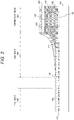
Fig. 2 is a cross-sectional view illustrating an example of the solid-state imaging element 100 in a first embodiment of the present technology. -
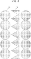
Fig. 3 is a planar view illustrating an example of a shape of adam 142 in the first embodiment of the present technology. -
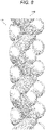
Fig. 4 is a perspective view illustrating an example of the shape of thedam 142 in the first embodiment of the present technology. -
Fig. 5 is a flow chart illustrating an example of a forming method of thedam 142 in the first embodiment of the present technology. -
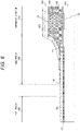
Fig. 6 is a cross-sectional view illustrating an example of a solid-state imaging element 100 in a second embodiment of the present technology. -
Fig. 7 is a planar view illustrating an example of a shape of adam 143 in the second embodiment of the present technology. -
Fig. 8 is a perspective view illustrating an example of the shape of thedam 143 in the second embodiment of the present technology. -
Fig. 9 is a view illustrating a system configuration example of anelectronic device 800 to which the embodiment of the present technology is applied. - A mode for carrying out the present technology (hereinafter, referred to as an embodiment) is hereinafter described. The description is given in the following order.
- 1. First Embodiment (example in which saw-tooth shape is provided partially in cylindrical shape of linear dam)
- 2. Second Embodiment (example in which basic structure of dam has saw-tooth shape)
- 3. Application Example (electronic device)
-
Fig. 1 is a planar view illustrating an example of a solid-state imaging element 100 in an embodiment of the present technology. - The solid-
state imaging element 100 is provided with apixel region 102, achip mounting region 103, and adam region 104 on asemiconductor substrate 101. Thesemiconductor substrate 101 includes as a main material, for example, silicon (Si) as a semiconductor. - The
pixel region 102 is a region in which a plurality of pixels having a photoelectric conversion unit that generates and accumulates photocharges according to an amount of received light is two-dimensionally arranged in a matrix in a row direction and in a column direction. - The
chip mounting region 103 is a region for flip-chip mounting a chip on which a circuit that performs predetermined signal processing is formed, for example. - The
dam region 104 is a region arranged around thechip mounting region 103. Thedam region 104 is provided with a dam for blocking an outflow of a resin from thechip mounting region 103. - A plurality of
electrode pads 109 is formed on an outer peripheral portion of the solid-state imaging element 100. Theelectrode pad 109 is used as a contact of a probe in an inspection process and wire bonding. -
Fig. 2 is a cross-sectional view illustrating an example of the solid-state imaging element 100 in a first embodiment of the present technology. The drawing illustrates a portion including ends of thepixel region 102 and thechip mounting region 103 and thedam region 104 therebetween. - In the
pixel region 102, a photodiode as the photoelectric conversion unit is formed for every pixel in thesemiconductor substrate 101, and an on-chip lens (OCL) 122 is formed for every pixel on thesemiconductor substrate 101. On an upper surface of the OCL 122, for example, an antireflection film (low reflection film) using a low temperature oxide (LTO) film is formed. Furthermore, acolor filter layer 121 that allows light of a predetermined wavelength of red (R), green (G), blue (B) and the like to pass is formed between theOCL 122 and thesemiconductor substrate 101. - The OCL 122 includes, for example, silicon nitride (SiN) or a resin material such as a styrene resin, an acrylic resin, a styrene acrylic copolymer resin, or a siloxane resin. Furthermore, as materials of the antireflection film, silicon nitride (SiN), hafnium oxide (HfO2), aluminum oxide (Al2O3), zirconium oxide (ZrO2), tantalum oxide (Ta2O5), titanium oxide (TiO2), lanthanum oxide (LA2O3), praseodymium oxide (Pr2O3), cerium oxide (CeO2), neodymium oxide (Nd2O3), promethium oxide (Pm2O3), samarium oxide (Sm2O3), europium oxide (Eu2O3), gadolinium oxide (Gd2O3), terbium oxide (Tb2O3), dysprosium oxide (Dy2O3), holmium oxide (Ho2O3), thulium oxide (Tm2O3), ytterbium oxide (Yb2O3), lutetium oxide (Lu2O3), yttrium oxide (Y2O3) and the like may be used.
- In the
chip mounting region 103, achip 130 is flip-chip mounted on thesemiconductor substrate 101. Specifically, anelectrode unit 139 of thechip 130 and anelectrode unit 159 of thesemiconductor substrate 101 are electrically connected to each other via asolder bump 155. - A clearance other than the
solder bump 155 between thechip 130 and thesemiconductor substrate 101 is filled with anunderfill resin 150 in order to fill a gap. Theunderfill resin 150 includes, for example, an ultraviolet (UV) curable resin, a thermosetting resin and the like, and is formed by being injected into the clearance between thechip 130 and thesemiconductor substrate 101 and then cured. - An upper surface and a side surface of the
chip 130 and theunderfill resin 150 around thechip 130 are covered with a light-shieldingresin 160 including a black resin and the like having a light-shielding property in order to prevent reflection. The light-shieldingresin 160 also includes an ultraviolet (UV) curable resin, a thermosetting resin and the like as is the case with theunderfill resin 150, and is formed by being applied using a dispenser and then cured. - In contrast, in the
dam region 104, thecolor filter layer 121 and theOCL 122 formed in thepixel region 102 are directly extended to be formed. In this example, thepixel region 102 and thedam region 104 are separated from each other by a distance corresponding to four pixels, and theOCL 122 and thecolor filter layer 121 are also formed in a region between thepixel region 102 and thedam region 104. The region between thepixel region 102 and thedam region 104 may be omitted, or may be considered as a part of thedam region 104. - Furthermore, a
slit 141 for blocking theunderfill resin 150 may be formed as a dam in thedam region 104. Since theslit 141 is covered with the light-shieldingresin 160, this does not affect reflection of incident light. - A
dam 142 for blocking the light-shieldingresin 160 is formed in an outer peripheral portion of thedam region 104. Note that, thedam 142 may have a function of blocking theunderfill resin 150. A shape of thedam 142 is described below. -
Fig. 3 is a planar view illustrating an example of the shape of thedam 142 in the first embodiment of the present technology. Furthermore,Fig. 4 is a perspective view illustrating an example of the shape of thedam 142 in the first embodiment of the present technology. - The
dam 142 has a saw-tooth shape toward an outer side of thedam region 104 in a semi-cylindrical shape obtained by linearly connecting theOCLs 122. This saw-tooth shape is provided at least partially in thedam region 104. For example, this may be provided partially or entirely on one side facing thepixel region 102. Furthermore, this may also be provided entirely on four sides. - In the saw-tooth shape (jagged shape) of the
dam 142, an angle of a projection is desirably 90 degrees or smaller. Therefore, the incident light is repeatedly reflected at an opening sandwiched between the projections to be attenuated. Therefore, occurrence of flare may be prevented. - Furthermore, since the
dam 142 has the shape obtained by linearly connecting theOCLs 122, a size of thedam 142 is an integral multiple of an arrangement pitch of theOCLs 122. -
Fig. 5 is a flow chart illustrating an example of a forming method of thedam 142 in the first embodiment of the present technology. - A circuit such as a light reception unit and a transfer channel region is formed on the
semiconductor substrate 101, and a transfer electrode, a light-shielding film and the like are formed (step S911). Moreover, after an interlayer insulating film is formed on an entire surface, a planarization film is formed, and thecolor filter layer 121 is formed thereon (step S912). - A lens material layer that becomes the
OCL 122 or thedam 142 is formed on the color filter layer 121 (step S913). The lens material layer is formed by, for example, applying a resin by spin coating and the like and curing the same. - Next, a resist is formed on the lens material layer using a pattern of the
OCL 122 and the dam 142 (step S914). Then, after the resist is patterned into the shape of theOCL 122 or thedam 142 by a photolithography process, for example, the resist is softened by heating and processed into the shape of theOCL 122 or thedam 142. - Then, the resist and the lens material layer in the shape of the
OCL 122 or thedam 142 are etched back (step S915). In this etching, for example, anisotropic reactive ion etching (RIE) using CF4/O2 as an etching gas may be used. - Therefore, a hemispherical shape of the resist is transferred to the lens material layer, and the shape of the
OCL 122 and thedam 142 is formed. - In this manner, according to the first embodiment of the present technology, by providing the
dam 142 having the saw-tooth shape toward the outer side of thedam region 104, it is possible to attenuate reflection of the incident light and prevent the occurrence of the flare. Then, an optical characteristic in thepixel region 102 may be improved with this arrangement. - In the first embodiment described above, the saw-tooth shape is provided partially in the linear cylindrical shape, but a basic structure of the dam is not necessarily linear. In this second embodiment, an example in which a basic structure of the dam has a saw-tooth shape is described. Note that, an entire configuration as a solid-
state imaging element 100 is similar to that of the above-described first embodiment, so that the detailed description thereof is omitted. -
Fig. 6 is a cross-sectional view illustrating an example of the solid-state imaging element 100 in the second embodiment of the present technology. - The solid-
state imaging element 100 according to the second embodiment is basically provided with a cross-sectional structure similar to that of the first embodiment described above. Note that, a structure of adam 143 for blocking a light-shieldingresin 160 formed in an outer peripheral portion of adam region 104 is different. A shape of thedam 143 is described below. -
Fig. 7 is a planar view illustrating an example of the shape of thedam 143 in the second embodiment of the present technology. Furthermore,Fig. 8 is a perspective view illustrating an example of the shape of thedam 143 in the second embodiment of the present technology. - The
dam 143 has a shape obtained by connectingOCLs 122 in a zigzag manner, and has a saw-tooth shape toward an outer side and an inner side of thedam region 104. Thedam 143 in the saw-tooth shape is provided at least partially in thedam region 104, and may have a linear semi-cylindrical shape in other parts. For example, this may be provided partially or entirely on one side facing thepixel region 102. Furthermore, this may also be provided entirely on four sides. Furthermore, thedam 142 of the first embodiment described above may be formed in the linear portion. - In the saw-tooth shape (jagged shape) of the
dam 143, an angle of a projection is desirably 90 degrees or smaller. Therefore, the incident light is repeatedly reflected at an opening sandwiched between the projections to be attenuated. Therefore, occurrence of flare may be prevented. - Furthermore, since the
dam 143 has the shape obtained by connecting theOCLs 122 in a zigzag manner, a size of the saw-tooth shape of thedam 143 is an integral multiple of an arrangement pitch of theOCLs 122. - Note that, the
dam 143 in the second embodiment is also formed in a manner similar to that in the first embodiment described above. - In this manner, according to the second embodiment of the present technology, by providing the
dam 143 having the saw-tooth shape toward the outer side of thedam region 104, it is possible to attenuate reflection of the incident light and prevent the occurrence of the flare. Then, an optical characteristic in thepixel region 102 may be improved with this arrangement. - Note that, in the first and second embodiments described above, an example in which one dam is arranged is described, but a plurality of dams may be arranged.
-
Fig. 9 is a view illustrating a system configuration example of anelectronic device 800 to which the embodiment of the present technology is applied. - The
electronic device 800 is a mobile terminal having a function as an imaging device. Thiselectronic device 800 is provided with animaging unit 810, ashutter button 830, apower button 840, acontrol unit 850, astorage unit 860, awireless communication unit 870, adisplay unit 880, and abattery 890. - The
imaging unit 810 is an image sensor that images a subject. Theimaging unit 810 is provided with the above-described solid-state imaging element 100. - The
shutter button 830 is a button for indicating an imaging timing by theimaging unit 810 from an outer side of theelectronic device 800. Thepower button 840 is a button for indicating turning on/off of the power of theelectronic device 800 from the outer side of theelectronic device 800. - The
control unit 850 is a processing unit that controls an entireelectronic device 800. Thestorage unit 860 is a memory that stores data and a program required for operation of theelectronic device 800. Thewireless communication unit 870 performs wireless communication with the outer side of theelectronic device 800. Thedisplay unit 880 is a display that displays an image and the like. Thebattery 890 is a power supply source that supplies power to each unit of theelectronic device 800. - Note that, the above-described embodiment describes an example of embodying the present technology, and there is a correspondence relationship between items in the embodiment and the matters specifying the invention in claims. Similarly, there is a correspondence relationship between the matters specifying the invention in claims and the matters in the embodiment of the present technology having the same names. However, the present technology is not limited to the embodiment and may be embodied by variously modifying the embodiment without departing from the gist thereof.
- Note that, the effect described in this specification is illustrative only and is not limitative; there may also be another effect.
- Note that, the present technology may also have a following configuration.
- (1) A solid-state imaging element provided with:
- a pixel region in which a plurality of pixels is arranged;
- a chip mounting region in which a chip is mounted; and
- a dam region arranged around the chip mounting region and having a saw-tooth shape toward an outer side at least partially.
- (2) The solid-state imaging element according to (1) described above, in which
in the saw-tooth shape in the dam region, an angle of a projection is 90 degrees or smaller. - (3) The solid-state imaging element according to (1) or (2) described above, in which
- the pixel region is provided with a first on-chip lens on an incident light side,
- the dam region is provided with a second on-chip lens having a same shape as a shape of the first on-chip lens, and
- the saw-tooth shape in the dam region is a structure obtained by connecting second on-chip lenses to each other.
- (4) The solid-state imaging element according to (3) described above, in which
a size of the saw-tooth shape in the dam region is an integral multiple of an arrangement pitch of the second on-chip lenses. - (5) The solid-state imaging element according (3) or (4) described above, further provided with:
an antireflection film formed on an upper surface of the second on-chip lens in the dam region. - (6) The solid-state imaging element according to any one of (1) to (5) described above, in which
the saw-tooth shape in the dam region is formed entirely on one side of the dam region. - (7) The solid-state imaging element according to any one of (1) to (5) described above, in which
the saw-tooth shape in the dam region is formed entirely on four sides of the dam region. - (8) The solid-state imaging element according to any one of (1) to (7) described above, in which
the saw-tooth shape in the dam region is a dam that blocks an outflow of a light-shielding resin that covers an upper surface and a side surface of the chip. - (9) The solid-state imaging element according to any one of (1) to (7) described above, in which
the saw-tooth shape in the dam region is a dam that blocks an outflow of an underfill resin that fills a range in which the chip is flip-chip mounted in the chip mounting region. - (10) An electronic device provided with:
a solid-state imaging element provided with: a pixel region in which a plurality of pixels is arranged; a chip mounting region in which a chip is mounted; and a dam region arranged around the chip mounting region and having a saw-tooth shape toward an outer side at least partially. -
- 100
- Solid-state imaging element
- 101
- Semiconductor substrate
- 102
- Pixel region
- 103
- Chip mounting region
- 104
- Dam region
- 109
- Electrode pad
- 121
- Color filter layer
- 122
- On-chip lens (OCL)
- 130
- Chip
- 139
- Electrode unit
- 141
- Slit
- 142, 143
- Dam
- 150
- Underfill resin
- 155
- Solder bump
- 159
- Electrode unit
- 160
- Light-shielding resin
- 800
- Electronic device
- 810
- Imaging unit
Claims (10)
- A solid-state imaging element comprising:a pixel region in which a plurality of pixels is arranged;a chip mounting region in which a chip is mounted; anda dam region arranged around the chip mounting region and having a saw-tooth shape toward an outer side at least partially.
- The solid-state imaging element according to claim 1, wherein
in the saw-tooth shape in the dam region, an angle of a projection is 90 degrees or smaller. - The solid-state imaging element according to claim 1, whereinthe pixel region is provided with a first on-chip lens on an incident light side,the dam region is provided with a second on-chip lens having a same shape as a shape of the first on-chip lens, andthe saw-tooth shape in the dam region is a structure obtained by connecting second on-chip lenses to each other.
- The solid-state imaging element according to claim 3, wherein
a size of the saw-tooth shape in the dam region is an integral multiple of an arrangement pitch of the second on-chip lenses. - The solid-state imaging element according to claim 3, further comprising:
an antireflection film formed on an upper surface of the second on-chip lens in the dam region. - The solid-state imaging element according to claim 1, wherein
the saw-tooth shape in the dam region is formed entirely on one side of the dam region. - The solid-state imaging element according to claim 1, wherein
the saw-tooth shape in the dam region is formed entirely on four sides of the dam region. - The solid-state imaging element according to claim 1, wherein
the saw-tooth shape in the dam region is a dam that blocks an outflow of a light-shielding resin that covers an upper surface and a side surface of the chip. - The solid-state imaging element according to claim 1, wherein
the saw-tooth shape in the dam region is a dam that blocks an outflow of an underfill resin that fills a range in which the chip is flip-chip mounted in the chip mounting region. - An electronic device comprising:
a solid-state imaging element provided with: a pixel region in which a plurality of pixels is arranged; a chip mounting region in which a chip is mounted; and a dam region arranged around the chip mounting region and having a saw-tooth shape toward an outer side at least partially.
Applications Claiming Priority (2)
| Application Number | Priority Date | Filing Date | Title |
|---|---|---|---|
| JP2020003397 | 2020-01-14 | ||
| PCT/JP2020/044823 WO2021145082A1 (en) | 2020-01-14 | 2020-12-02 | Solid-state imaging element and electronic device |
Publications (2)
| Publication Number | Publication Date |
|---|---|
| EP4092727A1 true EP4092727A1 (en) | 2022-11-23 |
| EP4092727A4 EP4092727A4 (en) | 2023-06-21 |
Family
ID=76864144
Family Applications (1)
| Application Number | Title | Priority Date | Filing Date |
|---|---|---|---|
| EP20913109.3A Withdrawn EP4092727A4 (en) | 2020-01-14 | 2020-12-02 | SOLID-STATE IMAGING ELEMENT AND ELECTRONIC DEVICE |
Country Status (5)
| Country | Link |
|---|---|
| US (1) | US12382741B2 (en) |
| EP (1) | EP4092727A4 (en) |
| JP (1) | JP7603022B2 (en) |
| CN (1) | CN114830336A (en) |
| WO (1) | WO2021145082A1 (en) |
Families Citing this family (3)
| Publication number | Priority date | Publication date | Assignee | Title |
|---|---|---|---|---|
| US20230238407A1 (en) * | 2020-06-22 | 2023-07-27 | Sony Semiconductor Solutions Corporation | Solid-state imaging device, method of manufacturing the same, and electronic device |
| US12193288B2 (en) * | 2021-12-09 | 2025-01-07 | Wuhan China Star Optoelectronics Semiconductor Display Technology Co., Ltd. | Display panel |
| CN120266262A (en) * | 2022-12-07 | 2025-07-04 | 索尼半导体解决方案公司 | Semiconductor packaging manufacturing method |
Citations (1)
| Publication number | Priority date | Publication date | Assignee | Title |
|---|---|---|---|---|
| JP2018147974A (en) | 2017-03-03 | 2018-09-20 | ソニーセミコンダクタソリューションズ株式会社 | Solid-state imaging device, electronic device, and semiconductor device |
Family Cites Families (7)
| Publication number | Priority date | Publication date | Assignee | Title |
|---|---|---|---|---|
| JP3541300B2 (en) * | 1994-09-21 | 2004-07-07 | イビデン株式会社 | Electronic component mounting equipment |
| JP4211014B2 (en) | 1997-09-25 | 2009-01-21 | 富士通株式会社 | Manufacturing method of semiconductor device |
| JP5211493B2 (en) * | 2007-01-30 | 2013-06-12 | 富士通セミコンダクター株式会社 | Wiring substrate and semiconductor device |
| JP5890272B2 (en) | 2012-07-26 | 2016-03-22 | 京セラ株式会社 | Light emitting element array and light emitting element head |
| TWI669810B (en) | 2014-09-11 | 2019-08-21 | 日商索尼半導體解決方案公司 | Solid-state imaging device, imaging device, electronic device, and semiconductor device |
| JP6295983B2 (en) * | 2015-03-05 | 2018-03-20 | ソニー株式会社 | SEMICONDUCTOR DEVICE, ITS MANUFACTURING METHOD, AND ELECTRONIC DEVICE |
| WO2018074581A1 (en) | 2016-10-21 | 2018-04-26 | ソニーセミコンダクタソリューションズ株式会社 | Electronic substrate and electronic device |
-
2020
- 2020-12-02 JP JP2021570671A patent/JP7603022B2/en active Active
- 2020-12-02 CN CN202080086632.8A patent/CN114830336A/en active Pending
- 2020-12-02 US US17/758,451 patent/US12382741B2/en active Active
- 2020-12-02 WO PCT/JP2020/044823 patent/WO2021145082A1/en not_active Ceased
- 2020-12-02 EP EP20913109.3A patent/EP4092727A4/en not_active Withdrawn
Patent Citations (1)
| Publication number | Priority date | Publication date | Assignee | Title |
|---|---|---|---|---|
| JP2018147974A (en) | 2017-03-03 | 2018-09-20 | ソニーセミコンダクタソリューションズ株式会社 | Solid-state imaging device, electronic device, and semiconductor device |
Also Published As
| Publication number | Publication date |
|---|---|
| CN114830336A (en) | 2022-07-29 |
| EP4092727A4 (en) | 2023-06-21 |
| JPWO2021145082A1 (en) | 2021-07-22 |
| JP7603022B2 (en) | 2024-12-19 |
| WO2021145082A1 (en) | 2021-07-22 |
| US20230036259A1 (en) | 2023-02-02 |
| US12382741B2 (en) | 2025-08-05 |
Similar Documents
| Publication | Publication Date | Title |
|---|---|---|
| USRE50032E1 (en) | Solid-state imaging device, method of manufacturing a solid-state imaging device, and electronic apparatus | |
| US12382741B2 (en) | Solid-state imaging element and electronic device | |
| US8223250B2 (en) | Solid-state image sensing device | |
| US7923798B2 (en) | Optical device and method for fabricating the same, camera module using optical device, and electronic equipment mounting camera module | |
| CN107425024B (en) | Solid-state imaging device, manufacturing method of solid-state imaging device, and electronic device | |
| CN108549121B (en) | Solid-state imaging device, method of manufacturing solid-state imaging device, and electronic apparatus | |
| JP4457142B2 (en) | Solid-state imaging device, camera module, and electronic information device | |
| US11043436B2 (en) | Semiconductor device, manufacturing method, imaging device, and electronic apparatus for enabling component mounting with high flatness | |
| CN110783350B (en) | Image sensing device including dummy pixels | |
| KR20230058729A (en) | Image picup element, image picup device, manufacturing device and method | |
| US12074180B2 (en) | Imaging element and method of manufacturing imaging element | |
| US10170516B2 (en) | Image sensing device and method for fabricating the same | |
| US12273605B2 (en) | Image sensor package and camera device comprising same | |
| JP5392458B2 (en) | Semiconductor image sensor | |
| US20250160012A1 (en) | Semiconductor device, electronic device, and manufacturing method for semiconductor device | |
| JP2010045082A (en) | Display element/electronic element module and its manufacturing method, and electronic information equipment | |
| JP4528879B2 (en) | Solid-state imaging device and manufacturing method thereof | |
| JP2011187482A (en) | Solid-state imaging apparatus, module for optical device, and method of manufacturing solid-state imaging apparatus | |
| CN108550597B (en) | Imaging device and electronic apparatus | |
| JP4521938B2 (en) | Imaging device | |
| JP2009295739A (en) | Semiconductor image sensor | |
| JPH06132506A (en) | Solid-state image sensor and manufacturing method thereof |
Legal Events
| Date | Code | Title | Description |
|---|---|---|---|
| STAA | Information on the status of an ep patent application or granted ep patent |
Free format text: STATUS: THE INTERNATIONAL PUBLICATION HAS BEEN MADE |
|
| PUAI | Public reference made under article 153(3) epc to a published international application that has entered the european phase |
Free format text: ORIGINAL CODE: 0009012 |
|
| STAA | Information on the status of an ep patent application or granted ep patent |
Free format text: STATUS: REQUEST FOR EXAMINATION WAS MADE |
|
| 17P | Request for examination filed |
Effective date: 20220523 |
|
| AK | Designated contracting states |
Kind code of ref document: A1 Designated state(s): AL AT BE BG CH CY CZ DE DK EE ES FI FR GB GR HR HU IE IS IT LI LT LU LV MC MK MT NL NO PL PT RO RS SE SI SK SM TR |
|
| DAV | Request for validation of the european patent (deleted) | ||
| DAX | Request for extension of the european patent (deleted) | ||
| REG | Reference to a national code |
Ref country code: DE Ref legal event code: R079 Free format text: PREVIOUS MAIN CLASS: H01L0023290000 Ipc: H01L0027146000 |
|
| A4 | Supplementary search report drawn up and despatched |
Effective date: 20230524 |
|
| RIC1 | Information provided on ipc code assigned before grant |
Ipc: H01L 27/146 20060101AFI20230517BHEP |
|
| STAA | Information on the status of an ep patent application or granted ep patent |
Free format text: STATUS: THE APPLICATION HAS BEEN WITHDRAWN |
|
| 18W | Application withdrawn |
Effective date: 20250423 |