EP4092717A1 - Sample support - Google Patents
Sample support Download PDFInfo
- Publication number
- EP4092717A1 EP4092717A1 EP21780318.8A EP21780318A EP4092717A1 EP 4092717 A1 EP4092717 A1 EP 4092717A1 EP 21780318 A EP21780318 A EP 21780318A EP 4092717 A1 EP4092717 A1 EP 4092717A1
- Authority
- EP
- European Patent Office
- Prior art keywords
- openings
- substrate
- sample support
- markers
- conductive layer
- Prior art date
- Legal status (The legal status is an assumption and is not a legal conclusion. Google has not performed a legal analysis and makes no representation as to the accuracy of the status listed.)
- Withdrawn
Links
Images






Classifications
-
- G—PHYSICS
- G03—PHOTOGRAPHY; CINEMATOGRAPHY; ANALOGOUS TECHNIQUES USING WAVES OTHER THAN OPTICAL WAVES; ELECTROGRAPHY; HOLOGRAPHY
- G03F—PHOTOMECHANICAL PRODUCTION OF TEXTURED OR PATTERNED SURFACES, e.g. FOR PRINTING, FOR PROCESSING OF SEMICONDUCTOR DEVICES; MATERIALS THEREFOR; ORIGINALS THEREFOR; APPARATUS SPECIALLY ADAPTED THEREFOR
- G03F7/00—Photomechanical, e.g. photolithographic, production of textured or patterned surfaces, e.g. printing surfaces; Materials therefor, e.g. comprising photoresists; Apparatus specially adapted therefor
- G03F7/004—Photosensitive materials
- G03F7/09—Photosensitive materials characterised by structural details, e.g. supports, auxiliary layers
-
- H—ELECTRICITY
- H01—ELECTRIC ELEMENTS
- H01J—ELECTRIC DISCHARGE TUBES OR DISCHARGE LAMPS
- H01J49/00—Particle spectrometers or separator tubes
- H01J49/02—Details
- H01J49/04—Arrangements for introducing or extracting samples to be analysed, e.g. vacuum locks; Arrangements for external adjustment of electron- or ion-optical components
- H01J49/0409—Sample holders or containers
- H01J49/0418—Sample holders or containers for laser desorption, e.g. matrix-assisted laser desorption/ionisation [MALDI] plates or surface enhanced laser desorption/ionisation [SELDI] plates
-
- G—PHYSICS
- G03—PHOTOGRAPHY; CINEMATOGRAPHY; ANALOGOUS TECHNIQUES USING WAVES OTHER THAN OPTICAL WAVES; ELECTROGRAPHY; HOLOGRAPHY
- G03F—PHOTOMECHANICAL PRODUCTION OF TEXTURED OR PATTERNED SURFACES, e.g. FOR PRINTING, FOR PROCESSING OF SEMICONDUCTOR DEVICES; MATERIALS THEREFOR; ORIGINALS THEREFOR; APPARATUS SPECIALLY ADAPTED THEREFOR
- G03F7/00—Photomechanical, e.g. photolithographic, production of textured or patterned surfaces, e.g. printing surfaces; Materials therefor, e.g. comprising photoresists; Apparatus specially adapted therefor
- G03F7/004—Photosensitive materials
- G03F7/0042—Photosensitive materials with inorganic or organometallic light-sensitive compounds not otherwise provided for, e.g. inorganic resists
- G03F7/0044—Photosensitive materials with inorganic or organometallic light-sensitive compounds not otherwise provided for, e.g. inorganic resists involving an interaction between the metallic and non-metallic component, e.g. photodope systems
-
- G—PHYSICS
- G03—PHOTOGRAPHY; CINEMATOGRAPHY; ANALOGOUS TECHNIQUES USING WAVES OTHER THAN OPTICAL WAVES; ELECTROGRAPHY; HOLOGRAPHY
- G03F—PHOTOMECHANICAL PRODUCTION OF TEXTURED OR PATTERNED SURFACES, e.g. FOR PRINTING, FOR PROCESSING OF SEMICONDUCTOR DEVICES; MATERIALS THEREFOR; ORIGINALS THEREFOR; APPARATUS SPECIALLY ADAPTED THEREFOR
- G03F7/00—Photomechanical, e.g. photolithographic, production of textured or patterned surfaces, e.g. printing surfaces; Materials therefor, e.g. comprising photoresists; Apparatus specially adapted therefor
- G03F7/16—Coating processes; Apparatus therefor
- G03F7/162—Coating on a rotating support, e.g. using a whirler or a spinner
Definitions
- the present disclosure relates to a sample support.
- a sample support used for ionizing a component of a sample
- a sample support which includes a substrate having a first surface, a second surface on a side opposite to the first surface, and a plurality of through-holes that are open on the first surface and on the second surface; a base bonded to the first surface of the substrate; and a conductive layer provided on the second surface of the substrate, and in which a plurality of openings are formed in the base (for example, refer to Patent Literature 1).
- each of a plurality of regions of the substrate corresponding to the plurality of openings can be used as a measurement region.
- Patent Literature 1 Japanese Patent No. 6539801
- an object of the present disclosure is to provide a sample support that makes highly accurate mass spectrometry possible.
- a sample support for ionizing a component of a sample, the support including: a substrate having a first surface, a second surface on a side opposite to the first surface, and a plurality of through-holes opening on the first surface and on the second surface; a first member having a plurality of first openings and disposed on the first surface; a second member having a plurality of second openings and disposed on the second surface, each of the plurality of second openings corresponding to each of the plurality of first openings in a thickness direction of the substrate; a bonding member disposed between the first member and the second member, and bonding the substrate and at least one of the first member and the second member; and a conductive layer integrally provided on a region of the second surface corresponding to each of the plurality of second openings, on a surface of the second member on a side opposite to the substrate, and on an inner surface of each of the plurality of second openings.
- the plurality of through-holes include a plurality of first through-holes located between each of the plurality of first openings and each of the plurality of second openings, and a plurality of second through-holes located between the first member and the second member. Each of the plurality of second openings communicates with each of the plurality of first openings through the plurality of first through-holes.
- each of the plurality of second openings of the second member communicates with each of the plurality of first openings of the first member through the plurality of first through-holes of the substrate. Accordingly, each of a plurality of the regions of the substrate corresponding to each of the plurality of second openings can be used as a measurement region.
- the substrate, the first member, and the second member can be unitized using the bonding member, and thereafter, the conductive layer can be provided from a second member side.
- the bonding member may be disposed in the plurality of second through-holes. According to this configuration, when each of the plurality of regions of the substrate corresponding to the plurality of second openings is used as the measurement region, each of a plurality of the measurement regions is isolated by the bonding member. For this reason, when the sample is disposed in each of the plurality of measurement regions, the movement of the sample between the measurement regions adjacent to each other is suppressed. Therefore, highly accurate mass spectrometry can be performed in each of the measurement regions.
- the bonding member may bond the first member and the substrate between the plurality of first openings and bond the second member and the substrate between the plurality of second openings.
- each of the first member and the second member may be made of a metal material. According to this configuration, a voltage can be stably applied to the conductive layer provided in the region of the second surface of the substrate, the region corresponding to each of the plurality of second openings.
- the bonding member may have conductivity. According to this configuration, a voltage can be stably applied to the conductive layer provided in the region of the second surface of the substrate, the region corresponding to each of the plurality of second openings.
- the bonding member may be made of a photocurable material.
- the bonding member may be made of an acrylic material or an epoxy material. According to this configuration, it is not necessary to perform a heat treatment for curing the bonding member. For this reason, even when a material that is greatly different in thermal expansion coefficient from a material of the substrate is used for at least one of the first member and the second member, the generation of bending caused by the heat treatment can be avoided.
- the sample support of the present disclosure may further include at least one of a plurality of first markers and a plurality of second markers, each of the plurality of first markers indicating each of the plurality of first openings when the first member is viewed from a side opposite to the substrate, each of the plurality of second markers indicating each of the plurality of second openings when the second member is viewed from a side opposite to the substrate.
- each of the plurality of regions of the substrate corresponding to each of the plurality of second openings is used as the measurement region, each of the plurality of measurement regions can be easily recognized by recognizing each of the plurality of first openings or each of the plurality of second openings.
- the first member may have a third surface on which the substrate is disposed, and a fourth surface located outside the substrate to face the same side as the third surface.
- a distance between a surface of the conductive layer on a side opposite to the substrate and the fourth surface may be smaller than a thickness of the substrate, the surface of the conductive layer is a surface of the conductive layer provided on the second surface.
- the focal point of the energy ray can be aligned with the surface of the conductive layer at a level less than the thickness of the substrate, by holding the first member with the adapter such that the reference surface of the adapter and the fourth surface of the first member are located on the same plane. For this reason, the focal point of the energy ray can be highly accurately aligned in the mass spectrometer.
- the fourth surface may extend to surround the substrate when viewed from the thickness direction. According to this configuration, the strength of the first member and consequently, the strength of the sample support can be improved. In addition, the first member can be easily and reliably held by the adapter described above.
- an outer edge each of the plurality of second openings may be located inside an outer edge each of the plurality of first openings when viewed from the thickness direction.
- a region of the substrate in which the first opening and the second opening overlap each other when viewed from the thickness direction is used as the measurement region, for example, when the outer edge of the second opening is located outside the outer edge of the first opening, a region defined by the outer edge of the second opening includes not only the measurement region but also other regions when the second member is viewed from the side opposite to the substrate. For this reason, it is difficult to identify a range of the measurement region, which is a concern.
- a region defined by the outer edge of the second opening is the measurement region, so that a range of the measurement region can be easily identified by identifying the outer edge of the second opening.
- a thickness of the second member may be smaller than a thickness of the first member.
- a sample support 1 shown in FIGS. 1 to 3 is used for ionizing a component of a sample.
- the sample support 1 includes a substrate 2, a base (first member) 3, a cover (second member) 4, a bonding member 5, and a conductive layer 6.
- the substrate 2 has a surface (first surface) 2a and a surface (second surface) 2b on a side opposite to the surface 2a.
- a plurality of through-holes 2c that are open on the surface 2a and on the surface 2b are formed in the substrate 2.
- Each of the through-holes 2c extends along a thickness direction D (hereinafter, simply referred to as a "direction D") of the substrate 2.
- the direction D is a direction in which the surface 2a and the surface 2b face each other.
- the substrate 2 is formed in a rectangular plate shape from an insulating material.
- a length of one side of the substrate 2 when viewed from the direction D is, for example, approximately several cm, and a thickness of the substrate 2 is, for example, 1 to 50 ⁇ m.
- a shape of each of the through-holes 2c when viewed from the direction D is, for example, a substantially circular shape, and a width of each of the through-holes 2c is, for example, 1 to 700 nm.
- the plurality of through-holes 2c each having a substantially constant width are uniformly (with a uniform distribution) formed in the substrate 2.
- An opening ratio of the through-holes 2c in a measurement region R (to be described later) (ratio of a region occupied by all the through-holes 2c to the measurement region R when viewed from the direction D) is practically 10 to 80%, particularly preferably 20 to 40%.
- the plurality of through-holes 2c may be irregular in the width of each of the through-holes 2c or the through-holes 2c may be partially connected to each other.
- the width of the through-holes 2c is a value obtained as follows. First, an image of each of the surface 2a and the surface 2b of the substrate 2 is acquired.
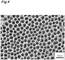
- FIG. 4 is a view showing a SEM image of the surface 2a of the substrate 2. In the SEM image, black portions are the through-holes 2c, and white portions are partition wall portions between the through-holes 2c.
- binarization processing is performed on the acquired image of the surface 2a to extract a plurality of pixel groups corresponding to a plurality of openings (openings on a surface 2a side of the through-holes 2c) in the measurement region R, and a diameter of a circle having an average area of the openings is acquired based on the size per one pixel.
- binarization processing is performed on the acquired image of the surface 2b to extract a plurality of pixel groups corresponding to a plurality of openings (openings on a surface 2b side of the through-holes 2c) in the measurement region R, and a diameter of a circle having an average area of the openings is acquired based on the size per one pixel. Then, an average value of the diameter of the circle acquired for the surface 2a and the diameter of the circle acquired for the surface 2b is acquired as a width of the through-holes 2c.
- the substrate 2 shown in FIG. 4 is an alumina porous film formed by anodizing aluminum (Al).
- the substrate 2 can be obtained by performing an anodizing treatment on an Al substrate and by peeling off an oxidized surface portion from the Al substrate.
- the substrate 2 may be formed by anodizing a valve metal other than Al, such as tantalum (Ta), niobium (Nb), titanium (Ti), hafnium (Hf), zirconium (Zr), zinc (Zn), tungsten (W), bismuth (Bi), or antimony (Sb) or may be formed by anodizing silicon (Si).
- the base 3 has a rectangular plate shape.
- the base 3 has a surface 3a and a surface (third surface) 3b on a side opposite to the surface 3a.
- a length of one side of the base 3 when viewed from the direction D is, for example, approximately several cm.
- an outer edge of the base 3 is located outside an outer edge of the substrate 2.
- a thickness (distance between the surface 3a and the surface 3b) of the base 3 is, for example, approximately 1 mm.
- a plurality of openings (first openings) 3c arranged in a twodimensional pattern (for example, a matrix pattern of 5 rows and 14 columns or the like) are formed in the base 3.
- Each of the plurality of openings 3c is defined by a partition wall portion 31 of the base 3.
- a shape of each of the openings 3c when viewed from the direction D is, for example, a circular shape, and in that case, a diameter of each of the openings 3c is, for example, approximately several mm to several tens of mm.
- the diameter of each of the openings 3c is, for example, approximately 3 mm.
- the base 3 includes a body portion 33 and a protrusion portion 34.
- the body portion 33 and the protrusion portion 34 are integrally formed.
- the plurality of openings 3c are formed in the body portion 33.
- the protrusion portion 34 protrudes from the surface 3b at a peripheral edge of the body portion 33.
- the protrusion portion 34 has a rectangular ring shape when viewed from the direction D. Namely, a recessed portion defined by the surface 3b and the protrusion portion 34 is formed in the base 3.
- the protrusion portion 34 extends to surround the plurality of openings 3c when viewed from the direction D.
- the protrusion portion 34 has a surface (fourth surface) 3d facing the same side as the surface 3b. The surface 3d extends to surround the plurality of openings 3c when viewed from the direction D.
- the base 3 is disposed on the surface 2a of the substrate 2. Specifically, the substrate 2 is disposed in the recessed portion of the base 3 such that the protrusion portion 34 is located outside the substrate 2.
- the substrate 2 is disposed on the surface 3b such that the surface 2a faces the surface 3b of the base 3.
- the protrusion portion 34 extends to surround the substrate 2 when viewed from the direction D.
- the surface 3d extends to surround the substrate 2 when viewed from the direction D.
- the base 3 has conductivity.
- the base 3 is made of a metal material.
- the base 3 is made of, for example, a material having the same thermal expansion coefficient as that of the material of the substrate 2 or a material having a lower thermal expansion coefficient than that of the material of the substrate 2 (for example, an iron nickel alloy (42 alloy), molybdenum, kovar, titanium, or the like when the material of the substrate 2 is alumina).
- the material of the base 3 is an iron nickel alloy.
- the sample support 1 includes a plurality of markers (first markers) 32.
- Each of the plurality of markers 32 indicates each of the plurality of openings 3c when the base 3 is viewed from a side opposite to the substrate 2.
- the plurality of markers 32 are provided on the surface 3a of the base 3 (surface of the base 3 on a side opposite to the substrate 2).
- Each of the plurality of markers 32 is provided to correspond one-to-one to each of the plurality of openings 3c.
- Each of the plurality of markers 32 is provided next to each of the plurality of openings 3c when viewed from the direction D.
- Each of the plurality of markers 32 is, for example, a number.
- Each of the plurality of markers 32 has such a width that each of the plurality of markers 32 can be visually recognized by a measurer.
- Each of the plurality of markers 32 is formed, for example, by forming protrusions and recesses in the surface 3a.
- Each of the plurality of markers 32 is provided, for example, by stamping or engraving using a laser.
- the cover 4 has, for example, a rectangular plate shape.
- the cover 4 has a surface 4a and a surface 4b on a side opposite to the surface 4a.
- a length of one side of the cover 4 when viewed from the direction D is, for example, approximately several cm.
- an outer edge of the cover 4 is located outside the outer edge of the substrate 2.
- a thickness of the cover 4 is smaller than a thickness of the base 3.
- the thickness of the cover 4 is, for example, approximately 0.2 mm.
- a plurality of openings (second openings) 4c arranged in a twodimensional pattern (for example, a matrix pattern of 5 rows and 14 columns or the like) are formed in the cover 4.
- Each of the plurality of openings 4c is defined by a partition wall portion 41 of the cover 4.
- a shape of each of the openings 4c when viewed from the direction D is, for example, a circular shape, and in that case, a diameter of each of the openings 4c is, for example, approximately several mm to several tens of mm.
- the diameter of each of the openings 4c is smaller than the diameter of each of the openings 3c.
- the diameter of each of the openings 4c is, for example, approximately 2.5 mm.
- the cover 4 is disposed on the surface 2b of the substrate 2. Specifically, the cover 4 is disposed such that the surface 4a of the cover 4 faces the surface 2b of the substrate 2.
- Each of the plurality of openings 4c of the cover 4 corresponds to each of the plurality of openings 3c of the base 3 in the direction D. Specifically, each of the plurality of openings 4c and each of the plurality of openings 3c face each other one-to-one in the direction D.
- a center line of each of the plurality of openings 4c and a center line of each of the plurality of openings 3c overlap each other. When viewed from the direction D, an outer edge of each of the plurality of openings 4c is located inside an outer edge of each of the plurality of openings 3c.
- Each of portions of the substrate 2 corresponds to each of regions in which each of the plurality of openings 4c and each of the plurality of openings 3c overlap each other when viewed from the direction D functions as the measurement region R for ionizing the sample.
- each of portions of the substrate 2 corresponding to the plurality of openings 4c functions as the measurement region R.
- each of the plurality of the measurement regions R is defined by the outer edge of each of the plurality of openings 4c.
- the cover 4 has conductivity.
- the cover 4 is made of a metal material.
- the cover 4 is made of, for example, a material having the same thermal expansion coefficient as that of the material of the substrate 2 or a material having a lower thermal expansion coefficient than that of the material of the substrate 2 (for example, an iron nickel alloy (42 alloy), molybdenum, kovar, titanium, or the like when the material of the substrate 2 is alumina).
- the material of the cover 4 is an iron nickel alloy.
- a material having the same thermal expansion coefficient as that of the material of the substrate 2 or a material having a lower thermal expansion coefficient than that of the material of the substrate 2 is used for at least one of the base 3 and the cover 4, so that the bending of the substrate 2 after bonding and sintering can be suppressed, and sufficient bonding between the substrate 2 and the sample and an improvement in sensitivity in mass spectrometry can be realized.
- the sample support 1 is manufactured, the sample support 1 in which the conductive layer 6 is formed is sintered, so that the crystallinity of the conductive layer 6 can be improved, and the sample support 1 more suitable for mass spectrometry can be obtained.
- the sample support 1 includes a plurality of markers (second markers) 42.
- Each of the plurality of markers 42 indicates each of the plurality of openings 4c when the cover 4 is viewed from a side opposite to the substrate 2.
- the plurality of markers 42 are provided on the surface 4b of the cover 4 (surface of the cover 4 on a side opposite to the substrate 2).
- Each of the plurality of markers 42 is provided to correspond one-to-one to each of the plurality of openings 4c.
- Each of the plurality of markers 42 is provided next to each of the plurality of openings 4c when viewed from the direction D.
- Each of the plurality of markers 42 is, for example, a number.
- Each of the plurality of markers 42 is provided to correspond one-to-one to each of the plurality of markers 32.
- the marker 42 and the marker 32 corresponding to each other are provided next to the opening 4c and the opening 3c corresponding to each other, respectively.
- the marker 42 and the marker 32 corresponding to each other are the same number.
- Each of the plurality of markers 42 has such a width that each of the plurality of markers 42 can be visually recognized by a measurer.
- Each of the plurality of markers 42 is formed, for example, by forming protrusions and recesses in the surface 4b.
- Each of the plurality of markers 42 is provided, for example, by stamping or engraving using a laser.
- the plurality of through-holes 2c of the substrate 2 include a plurality of first through-holes 2d and a plurality of second through-holes 2e.
- the plurality of first through-holes 2d are located between each of the plurality of openings 3c and each of the plurality of openings 4c.
- each of the measurement regions R of the substrate 2 includes the plurality of first through-holes 2d.
- the plurality of second through-holes 2e are located between the base 3 and the cover 4.
- the plurality of second through-holes 2e are located between the partition wall portion 31 of the base 3 and the partition wall portion 41 of the cover 4.
- Each of the plurality of openings 3c and each of the plurality of openings 4c corresponding to each other communicates with each other through the plurality of first through-holes 2d.
- the bonding member 5 is disposed between the base 3 and the cover 4.
- the bonding member 5 bonds the base 3 and the substrate 2 between the plurality of openings 3c and bonds the cover 4 and the substrate 2 between the plurality of openings 4c.
- the bonding member 5 is integrally (continuously) disposed in the plurality of second through-holes 2e, between the partition wall portion 31 of the base 3 and the substrate 2, between the partition wall portion 41 of the cover 4 and the substrate 2, and between a side surface of the substrate 2 and the protrusion portion 34 of the base 3.
- the bonding member 5 is covered with the cover 4 when viewed from the direction D.
- the bonding member 5 overlaps the partition wall portion 41 of the cover 4 when viewed from the direction D.
- the bonding member 5 is not exposed to each of the plurality of openings 4c.
- the bonding member 5 has conductivity.
- the bonding member 5 may be made of a conductive adhesive agent or may be formed by applying a metal paste.
- the bonding member 5 is made of a UV curable material (photocurable material).
- the bonding member 5 is made of an acrylic material or an epoxy material. It is preferable that a bonding material that releases a small amount of gas (for example, an adhesive agent for use in vacuum or the like) is used as the material of the bonding member 5.
- the conductive layer 6 is integrally (continuously) provided in a region of the surface 2b of the substrate 2, the region corresponding to each of the plurality of openings 4c of the cover 4 (namely, a region of the surface 2b of the substrate 2, the region corresponding to each of the plurality of measurement regions R), an inner surface of each of the plurality of openings 4c, and the surface 4b of the cover 4.
- the conductive layer 6 covers a region of the surface 2b of the substrate 2 in each of the measurement regions R, the plurality of through-holes 2c not being formed in the region.
- the conductive layer 6 covers the markers 42 on the surface 4b of the cover 4. However, since the markers 42 are formed by forming protrusions and recesses in the surface 4b, even when the markers 42 are covered with the conductive layer 6, the visual recognition of the markers 42 is not interfered with.
- a surface 6a of the conductive layer 6 on a side opposite to the substrate 2 in each of the measurement regions R and the surface 3d of the protrusion portion 34 are located on the same plane (the same plane perpendicular to the direction D), the conductive layer 6 being formed on the surface 2b of the substrate 2. Namely, a distance between the surface 6a and the surface 3d in the direction D is 0 in the present embodiment and is smaller than the thickness of the substrate 2.
- the conductive layer 6 is made of a conductive material. Meanwhile, it is preferable that as the material of the conductive layer 6, metal having a low affinity (reactivity) with the sample and a high conductivity is used for reasons to be described below.
- metal having a low affinity (reactivity) with the sample and a high conductivity is used for reasons to be described below.
- the conductive layer 6 is made of metal such as copper (Cu) having a high affinity with a sample such as a protein
- Cu copper
- the sample is ionized in a state where Cu atoms adhere to molecules of the sample and, as a result, the ionized sample is detected as Cu adducts, so that a detection result shifts, which is a concern. Therefore, it is preferable that metal having a low affinity with a sample is used as the material of the conductive layer 6.
- the material of the conductive layer 6 is metal capable of efficiently transmitting the energy of laser light with which the substrate 2 is irradiated, to the sample through the conductive layer 6.
- the material of the conductive layer 6 is Al, gold (Au), platinum (Pt), or the like having a high absorptivity in the ultraviolet region.
- the conductive layer 6 is formed with a thickness of approximately 1 nm to 350 nm, for example, by a plating method, an atomic layer deposition (ALD) method, an evaporation method, a sputtering method, or the like.
- ALD atomic layer deposition
- evaporation method evaporation method
- sputtering method evaporation method
- chromium (Cr) nickel (Ni), titanium (Ti), or the like may be used as the material of the conductive layer 6.
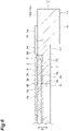
- the adapter 10 shown in FIGS. 5 and 6 is used for mounting the sample support 1 described above in a mass spectrometer.
- the adapter 10 includes a holding unit 11.
- the holding unit 11 includes a body member 12, a plurality of stoppers 13, and a plurality of sets of washers 14 and bolts 15.
- the body member 12 is formed in a rectangular frame shape from a metal material.
- the plurality of stoppers 13 are provided in the body member 12 to protrude to an inside of the body member 12.
- the plurality of sets of washers 14 and bolts 15 are attachable to and detachable from one surface 12a of the body member 12.
- the holding unit 11 has a reference surface 11a located on the same plane as a focal point of laser light in the mass spectrometer (the same plane parallel to an optical axis of the laser light).
- the reference surface 11a is the surface 12a of the body member 12.
- a distance between the surface 3a and the surface 3d of the base 3 in the direction D may be substantially equal to a predetermined distance between a part of each of the washers 14 and the corresponding stopper 13.
- the sample support 1 is disposed on the plurality of stoppers 13, and in that state, the plurality of sets of washers 14 and bolts 15 are fixed to the surface 12a of the body member 12, so that the sample support 1 is held by the holding unit 11.
- the reference surface 11a of the holding unit 11 and the surface 3d of the base 3 are located on the same plane (the same plane parallel to the direction D and to the optical axis of the laser light).
- the holding unit 11 holds the base 3 such that the reference surface 11a of the holding unit 11 and the surface 3d of the base 3 are located on the same plane.
- the sample support 1 is prepared.
- a sample S is disposed in each of the measurement regions R of the sample support 1.
- a solution containing the sample S is dripped on each of the measurement regions R from the surface 2b side of the substrate 2. Accordingly, in each of the measurement regions R, the excessive solution infiltrates into the plurality of through-holes 2c, and a component S1 of the sample S is appropriately held on the conductive layer 6.
- the sample support 1 on which the sample S is disposed in each of the measurement regions R is mounted in a mass spectrometer 100 using the adapter 10.
- a laser light irradiation unit 102 of the mass spectrometer 100 is operated to irradiate each of the measurement regions R with laser light (energy ray) L while applying a voltage to the conductive layer 6 of the sample support 1 through the adapter 10 by operating a voltage application unit 101 of the mass spectrometer 100. Accordingly, the component S1 of the sample S is ionized.
- the focal point P of the laser light L and the reference surface 11a of the holding unit 11 are located on the same plane, the reference surface 11a of the holding unit 11 and the surface 3d of the base 3 are located on the same plane, and the surface 3d of the base 3 and the surface 6a of the conductive layer 6 are located on the same plane, the focal point P of the laser light L is located on the surface 6a of the conductive layer 6 on which the component S1 of the sample S is held.
- the above steps correspond to the ionization method (in the present embodiment, a laser desorption and ionization method) using the sample support 1 and the adapter 10.
- sample ions S2 released by the ionization of the component S1 of the sample S are detected in an ion detection unit 103 of the mass spectrometer 100.
- the released sample ions S2 move toward a ground electrode provided between the sample support 1 and the ion detection unit 103, in an accelerated manner because of a potential difference generated between the conductive layer 6 to which the voltage has been applied and the ground electrode, and are detected by the ion detection unit 103.
- the mass spectrometer 100 is a scanning type mass spectrometer using a time-of-flight mass spectrometry (TOF-MS) method. The above steps correspond to the mass spectrometry method using the sample support 1 and the adapter 10.
- TOF-MS time-of-flight mass spectrometry
- FIGS. 1 and 5 to 7 the illustration of the conductive layer 6 is omitted.
- the illustration of the plurality of through-holes 2c is omitted.
- the illustration of some openings 3c and some openings 4c is omitted. Namely, in FIGS. 1 , 2 , and 5 , the number of the openings 3c and the openings 4c is shown as being smaller than an actual number.
- the illustration of some first through-holes 2d and some second through-holes 2e is omitted. Namely, in FIG. 3 , the number of the first through-holes 2d and the second through-holes 2e is shown as being smaller than an actual number.
- each of the plurality of openings 4c of the cover 4 communicates with each of the plurality of openings 3c of the base 3 through the plurality of first through-holes 2d of the substrate 2. Accordingly, each of a plurality of regions of the substrate 2 corresponds to each of the plurality of openings 4c can be used as the measurement region R.
- the substrate 2, the base 3, and the cover 4 can be unitized using the bonding member 5, and thereafter, the conductive layer 6 can be provided from a cover 4 side.
- FIG. 8 are graphs showing mass spectra obtained by a mass spectrometry method of a first example.
- (c) and (d) in FIG. 8 are graphs showing mass spectra obtained by a mass spectrometry method of a first comparative example.
- the sample support 1 is used in the mass spectrometry method of the first example.
- a sample support used in the mass spectrometry method of the first comparative example is different from the sample support 1 mainly in that the cover 4 is not provided.
- FIG. 8 in the first example, there is less noise in detected signal than in the first comparative example.
- FIG. 9 is a graph showing a mass spectrum obtained by a mass spectrometry method of a second comparative example.
- (b) in FIG. 9 is a graph showing a mass spectrum obtained by a mass spectrometry method of a second example.
- (c) in FIG. 9 is a graph showing a mass spectrum obtained by a mass spectrometry method of a third comparative example.
- (d) in FIG. 9 is a graph showing a mass spectrum obtained by a mass spectrometry method of a third example.
- the sample support 1 is used in the mass spectrometry method of each of the second example and the third example.
- a sample support used in the mass spectrometry method of each of the second comparative example and the third comparative example is different from the sample support 1 mainly in that the cover 4 is not provided.
- the second example there is less noise in detected signal than in the second comparative example.
- the third example there is less noise in detected signal than in the third comparative example.
- the bonding member 5 is disposed in the plurality of second through-holes 3e. According to this configuration, when each of the plurality of regions of the substrate 2 corresponding to the plurality of openings 4c is used as the measurement region R, each of the plurality of measurement regions R is isolated by the bonding member 5. For this reason, when the sample S is disposed in each of the plurality of measurement regions R, the movement of the sample S between the measurement regions R adjacent to each other is suppressed. Therefore, highly accurate mass spectrometry can be performed in each of the measurement regions R.
- the bonding member 5 bonds the base 3 and the substrate 2 between the plurality of openings 3c and bonds the cover 4 and the substrate 2 between the plurality of openings 4c.
- each of the base 3 and the cover 4 is made of a metal material. According to this configuration, a voltage can be stably applied to the conductive layer 6 provided in the region of the surface 2b of the substrate 2, the region corresponding to each of the plurality of openings 4c.
- the bonding member 5 has conductivity. According to this configuration, a voltage can be stably applied to the conductive layer 6 provided in the region of the surface 2b of the substrate 2, the region corresponding to each of the plurality of openings 4c.
- the bonding member 5 is made of a UV curable material.
- the bonding member 5 is made of an acrylic material or an epoxy material. According to this configuration, it is not necessary to perform a heat treatment for curing the bonding member 5. For this reason, even when a material that is greatly different in thermal expansion coefficient from the material of the substrate 2 is used for at least one of the base 3 and the cover 4, the generation of bending caused by the heat treatment can be avoided.
- the sample support 1 includes the plurality of markers 32 and the plurality of markers 42.
- Each of the plurality of markers 32 indicates each of the plurality of openings 3c when the base 3 is viewed from the side opposite to the substrate 2.
- Each of the plurality of markers 42 indicates each of the plurality of openings 4c when the cover 4 is viewed from the side opposite to the substrate 2.
- a solution containing the sample S may be dripped on the measurement regions R from the surface 2a side of the substrate 2 depending on the type of the solution. Namely, when the substrate 2 has a higher affinity with the solution than the conductive layer 6, it is preferable that the solution is dropped from the surface 2a side of the substrate 2. Accordingly, the solution can more smoothly flow into the first through-holes 2d than when the solution is dripped from the surface 2b side of the substrate 2.
- the sample support 1 since the sample support 1 includes both each of the plurality of markers 32 indicating each of the plurality of openings 3c, and each of the plurality of markers 42 indicating each of the plurality of openings 4c, when the solution is dripped from the surface 2a side of the substrate 2, the measurement regions R can be recognized by recognizing the openings 3c through the markers 32, and thereafter, when irradiation with the laser light L is performed, the measurement regions R can be recognized by recognizing the openings 4c through the markers 42.
- the base 3 has the surface 3b on which the substrate 2 is disposed, and the surface 3d located outside the substrate 2 to face the same side as the surface 3b, and the distance between the surface 6a of the conductive layer 6 and the surface 3d is smaller than the thickness of the substrate 2.
- the focal point P of the laser light L can be aligned with the surface 6a of the conductive layer 6 at a level less than the thickness of the substrate 2, by holding the base 3 with the adapter 10 such that the reference surface 11a of the adapter 10 and the surface 3d of the base 3 are located on the same plane. For this reason, the focal point P of the laser light L can be highly accurately aligned in the mass spectrometer 100.
- the protrusion portion 34 of the base 3 extends to surround the substrate 2 when viewed from the direction D. According to this configuration, the strength of the base 3 and consequently, the strength of the sample support 1 can be improved. In addition, the base 3 can be easily and reliably held by the adapter 10 described above.
- the outer edge of each of the plurality of openings 4c is located inside the outer edge of each of the plurality of openings 3c when viewed from the direction D.
- a region of the substrate 2 in which the opening 3c and the opening 4c overlap each other when viewed from the direction D is used as the measurement region R, for example, when the outer edge of the opening 4c is located outside the outer edge of the opening 3c, a region defined by the outer edge of the opening 4c includes not only the measurement region R but also other regions when the cover 4 is viewed from the side opposite to the substrate 2. For this reason, it is difficult to identify a range of the measurement region R, which is a concern.
- a region defined by the outer edge of the opening 4c is the measurement region R, so that a range of the measurement region R can be easily identified by identifying the outer edge of the opening 4c.
- the thickness of the cover 4 is smaller than the thickness of the base 3. According to this configuration, for example, when the sample support 1 is mounted in the mass spectrometer 100 using the adapter 10 having the reference surface 11a located on the same plane as the focal point P of the laser light L in the mass spectrometer 100, even though the cover 4 protrudes from the reference surface 11a of the adapter 10 in a state where the base 3 is held by the adapter 10, the interference of the sample support 1 with the mass spectrometer 100 can be suppressed.
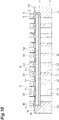
- the bonding member 5 bonds the base 3 and the substrate 2 between the plurality of openings 3c and bonds the cover 4 and the substrate 2 between the plurality of openings 4c, but the present disclosure is not limited to the example.
- the bonding member 5 may not bond the base 3 and the substrate 2 between the plurality of openings 3c.
- the bonding member 5 may not be disposed between the partition wall portion 31 of the base 3 and the substrate 2 between the plurality of openings 3c.
- the bonding member 5 may be disposed or not disposed between the partition wall portion 31 of the base 3 and the substrate 2 outside the plurality of openings 3c (at an outer edge portion of the substrate 2).
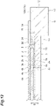
- the bonding member 5 may be disposed or not disposed between the side surface of the substrate 2 and the protrusion portion 34 of the base 3. In addition, as shown in FIG. 11 , the bonding member 5 may not bond the cover 4 and the substrate 2 between the plurality of openings 4c. Namely, the bonding member 5 may not be disposed between the partition wall portion 41 of the cover 4 and the substrate 2 between the plurality of openings 4c. Incidentally, the bonding member 5 may be disposed or not disposed between the partition wall portion 41 of the cover 4 and the substrate 2 outside the plurality of openings 4c (at the outer edge portion of the substrate 2). As described above, the bonding member 5 may be disposed between the base 3 and the cover 4 to bond the substrate 2 and at least one of the base 3 and the cover 4.
- the surface 6a of the conductive layer 6 and the surface 3d of the base 3 may not be located on the same plane perpendicular to the direction D. Even in this case, the focal point P of the laser light L can be aligned with the surface 6a of the conductive layer 6 at a level less than the thickness of the substrate 2, by holding the base 3 with the adapter 10 such that the reference surface 11a of the adapter 10 and the surface 3d of the base 3 are located on the same plane.
- the holding unit 11 of the adapter 10 can hold the base 3 such that the reference surface 11a of the adapter 10 and the surface 3d of the base 3 are located on the same plane, the present disclosure is not limited to the above-described configuration (namely, including the body member 12, the plurality of stoppers 13, and the plurality of sets of washers 14 and bolts 15).
- the body portion 33 and the protrusion portion 34 of the base 3 are integrally formed, but as shown in FIG. 12 , the body portion 33 and the protrusion portion 34 may be separately formed.
- the protrusion portion 34 may be made of, for example, an adhesive agent or evaporated metal.
- the base 3 may include a plurality of the protrusion portions arranged along an outer edge of the substrate 2 when viewed from the direction D. Each of the plurality of protrusion portions corresponds to each of the plurality of sets of washers 14 and bolts 15.
- the base 3 may not include the protrusion portion 34.
- Recessed portions (counterbores) each having substantially the same depth as a thickness of the protrusion portion 34 may be formed in the surface 12a of the body member 12.
- the sample support 1 is disposed on the plurality of stoppers 13, and in that state, the plurality of sets of washers 14 and bolts 15 are fixed to bottom surfaces of the recessed portions formed in the body member 12, so that the sample support 1 is held by the holding unit 11.
- the holding unit 11 holds the base 3 such that the bottom surfaces of the recessed portions formed in the body member 12 and the surface 3b of the base 3 are located on the same plane. Even in this case, the focal point P of the laser light L can be aligned with the surface 6a of the conductive layer 6 at a level less than the thickness of the substrate 2.
- the bonding member 5 is made of a UV curable material, but the bonding member 5 may be made of an inorganic binder or the like.
- the inorganic binder include Ceramabond (registered trademark) manufactured by Audec Co., Ltd., Aron Ceramic (registered trademark) manufactured by TOAGOSEI CO., LTD., and the like.
- each of the plurality of markers 32 is a number, but each of the plurality of markers 32 may be various markers.
- Each of the plurality of markers 32 may be at least one selected from, for example, a number, a symbol, and a character.
- each of the plurality of markers 42 is a number, but each of the plurality of markers 42 may be various markers.
- Each of the plurality of markers 42 may be at least one selected from, for example, a number, a symbol, and a character.
- each of the plurality of markers 32 is formed by forming protrusions and recesses in the surface 3a of the base 3, but each of the plurality of markers 32 may be formed by, for example, printing a character using printing such as nanoprinting, photolithography using extreme ultraviolet (EUV) exposure, writing with paint, blacking (oxidation) that is one example of engraving using a laser, or the like.
- printing a character using printing such as nanoprinting, photolithography using extreme ultraviolet (EUV) exposure
- EUV extreme ultraviolet
- writing with paint blacking (oxidation) that is one example of engraving using a laser, or the like.
- each of the plurality of markers 42 is formed by forming protrusions and recesses in the surface 4b of the cover 4, but each of the plurality of markers 42 may be formed by, for example, printing a character using printing such as nanoprinting, photolithography using extreme ultraviolet (EUV) exposure, writing with paint, blacking (oxidation) that is one example of engraving using a laser, or the like.
- EUV extreme ultraviolet
- the conductive layer 6 is not formed in regions of the surface 4b of the cover 4, the plurality of markers 42 being formed in the regions.
- each of the plurality of markers 32 is provided to correspond one-to-one to each of the plurality of openings 3c and is provided next to each of the plurality of openings 3c when viewed from the direction D, but each of the plurality of markers 32 may be arranged along rows and columns of the plurality of openings 3c outside the plurality of openings 3c.
- the plurality of markers 32 may form a coordinate system for identifying each of the plurality of openings 3c.
- each of the plurality of markers 42 is provided to correspond one-to-one to each of the plurality of openings 4c and is provided next to each of the plurality of openings 4c when viewed from the direction D, but each of the plurality of markers 42 may be arranged along rows and columns of the plurality of openings 4c outside the plurality of openings 4c.
- the plurality of markers 42 may form a coordinate system for identifying each of the plurality of openings 4c.
- each of the plurality of markers 32 is provided in the surface 3a of the base 3, but for example, when the conductive layer 6 is provided on the surface 3a of the base 3, each of the plurality of markers 32 may be provided in a surface of the conductive layer 6 provided on the surface 3a.
- each of the plurality of markers 42 is provided in the surface 4b of the cover 4, but each of the plurality of markers 42 may be provided in, for example, the surface 6a of the conductive layer 6, the surface 3d of the base 3, or the like.
- a solution containing the sample S is dripped on each of the measurement regions R from the surface 2b side of the substrate 2, but the solution may be dripped on each of the measurement regions R from the surface 2a side of the substrate 2.
- the solution is dripped from the surface 2a side of the substrate 2. Specifically, in a state where the sample support 1 is supported such that the surface 2a is located on an upper side with respect to the surface 2b, the solution is dripped on each of the measurement regions R from the surface 2a side.
- the sample support 1 includes both the plurality of markers 32 and the plurality of markers 42.
- Each of the plurality of markers 32 indicates each of the plurality of openings 3c.
- Each of the plurality of markers 42 indicates each of the plurality of openings 4c.
- the sample support 1 includes the plurality of markers 32 and the plurality of markers 42, but the sample support 1 may not include one of the plurality of markers 32 and the plurality of markers 42. Namely, the sample support 1 may include at least one of the plurality of markers 32 and the plurality of markers 42.
- the conductive layer 6 may be provided or not provided on the surface 2a of the substrate 2 and on an inner surface of each of the through-holes 2c.
- the application of the sample support 1 is not limited to the ionization of the sample S by irradiation with the laser light L.
- the sample support 1 can be used for the ionization of the sample S by irradiation with an energy ray such as laser light, an ion beam, or an electron beam.
- the sample S can be ionized by irradiation with an energy ray.
Landscapes
- Physics & Mathematics (AREA)
- General Physics & Mathematics (AREA)
- Chemical & Material Sciences (AREA)
- Optics & Photonics (AREA)
- Analytical Chemistry (AREA)
- Engineering & Computer Science (AREA)
- Architecture (AREA)
- Structural Engineering (AREA)
- Organic Chemistry (AREA)
- Other Investigation Or Analysis Of Materials By Electrical Means (AREA)
Abstract
Description
- The present disclosure relates to a sample support.
- As a sample support used for ionizing a component of a sample, a sample support has been known which includes a substrate having a first surface, a second surface on a side opposite to the first surface, and a plurality of through-holes that are open on the first surface and on the second surface; a base bonded to the first surface of the substrate; and a conductive layer provided on the second surface of the substrate, and in which a plurality of openings are formed in the base (for example, refer to Patent Literature 1). In such a sample support, each of a plurality of regions of the substrate corresponding to the plurality of openings can be used as a measurement region.
- Patent Literature 1:
Japanese Patent No. 6539801 - In the case of manufacturing the above-described sample support, when the first surface of the substrate and the base are bonded together, if a bonding member reaches the second surface of the substrate through the through-holes of the substrate before being cured, when the conductive layer is provided on the second surface of the substrate, outgas is generated from the conductive layer and from the bonding member, and a mixed layer caused by the outgas is deposited on the substrate, which is a concern. When the mixed layer is deposited on the substrate, noise caused by the mixed layer is generated in mass spectrometry, which is a concern.
- Therefore, an object of the present disclosure is to provide a sample support that makes highly accurate mass spectrometry possible.
- According to the present disclosure, there is provided a sample support for ionizing a component of a sample, the support including: a substrate having a first surface, a second surface on a side opposite to the first surface, and a plurality of through-holes opening on the first surface and on the second surface; a first member having a plurality of first openings and disposed on the first surface; a second member having a plurality of second openings and disposed on the second surface, each of the plurality of second openings corresponding to each of the plurality of first openings in a thickness direction of the substrate; a bonding member disposed between the first member and the second member, and bonding the substrate and at least one of the first member and the second member; and a conductive layer integrally provided on a region of the second surface corresponding to each of the plurality of second openings, on a surface of the second member on a side opposite to the substrate, and on an inner surface of each of the plurality of second openings. The plurality of through-holes include a plurality of first through-holes located between each of the plurality of first openings and each of the plurality of second openings, and a plurality of second through-holes located between the first member and the second member. Each of the plurality of second openings communicates with each of the plurality of first openings through the plurality of first through-holes.
- In the sample support, each of the plurality of second openings of the second member communicates with each of the plurality of first openings of the first member through the plurality of first through-holes of the substrate. Accordingly, each of a plurality of the regions of the substrate corresponding to each of the plurality of second openings can be used as a measurement region. Here, when the sample support is manufactured, the substrate, the first member, and the second member can be unitized using the bonding member, and thereafter, the conductive layer can be provided from a second member side. Accordingly, when the conductive layer is provided from the second member side, since the bonding member is disposed between the first member and the second member, outgas is unlikely to be generated from the conductive layer and the bonding member and, as a result, a mixed layer caused by the outgas can be prevented from being deposited on the substrate. As a result, according to this sample support, highly accurate mass spectrometry is possible.
- In the sample support of the present disclosure, the bonding member may be disposed in the plurality of second through-holes. According to this configuration, when each of the plurality of regions of the substrate corresponding to the plurality of second openings is used as the measurement region, each of a plurality of the measurement regions is isolated by the bonding member. For this reason, when the sample is disposed in each of the plurality of measurement regions, the movement of the sample between the measurement regions adjacent to each other is suppressed. Therefore, highly accurate mass spectrometry can be performed in each of the measurement regions.
- In the sample support of the present disclosure, the bonding member may bond the first member and the substrate between the plurality of first openings and bond the second member and the substrate between the plurality of second openings. According to this configuration, as described above, when each of the plurality of regions of the substrate corresponding to the plurality of second openings is used as the measurement region, the movement of the sample between the measurement regions adjacent to each other is more reliably suppressed. Therefore, more highly accurate mass spectrometry can be performed in each of the measurement regions.
- In the sample support of the present disclosure, each of the first member and the second member may be made of a metal material. According to this configuration, a voltage can be stably applied to the conductive layer provided in the region of the second surface of the substrate, the region corresponding to each of the plurality of second openings.
- In the sample support of the present disclosure, the bonding member may have conductivity. According to this configuration, a voltage can be stably applied to the conductive layer provided in the region of the second surface of the substrate, the region corresponding to each of the plurality of second openings.
- In the sample support of the present disclosure, the bonding member may be made of a photocurable material. For example, the bonding member may be made of an acrylic material or an epoxy material. According to this configuration, it is not necessary to perform a heat treatment for curing the bonding member. For this reason, even when a material that is greatly different in thermal expansion coefficient from a material of the substrate is used for at least one of the first member and the second member, the generation of bending caused by the heat treatment can be avoided.
- The sample support of the present disclosure may further include at least one of a plurality of first markers and a plurality of second markers, each of the plurality of first markers indicating each of the plurality of first openings when the first member is viewed from a side opposite to the substrate, each of the plurality of second markers indicating each of the plurality of second openings when the second member is viewed from a side opposite to the substrate. According to this configuration, when each of the plurality of regions of the substrate corresponding to each of the plurality of second openings is used as the measurement region, each of the plurality of measurement regions can be easily recognized by recognizing each of the plurality of first openings or each of the plurality of second openings.
- In the sample support of the present disclosure, the first member may have a third surface on which the substrate is disposed, and a fourth surface located outside the substrate to face the same side as the third surface. A distance between a surface of the conductive layer on a side opposite to the substrate and the fourth surface may be smaller than a thickness of the substrate, the surface of the conductive layer is a surface of the conductive layer provided on the second surface. According to this configuration, when the sample support is mounted in a mass spectrometer using an adapter having a reference surface located on the same plane as a focal point of an energy ray such as laser light in the mass spectrometer, the focal point of the energy ray can be aligned with the surface of the conductive layer at a level less than the thickness of the substrate, by holding the first member with the adapter such that the reference surface of the adapter and the fourth surface of the first member are located on the same plane. For this reason, the focal point of the energy ray can be highly accurately aligned in the mass spectrometer.
- In the sample support of the present disclosure, the fourth surface may extend to surround the substrate when viewed from the thickness direction. According to this configuration, the strength of the first member and consequently, the strength of the sample support can be improved. In addition, the first member can be easily and reliably held by the adapter described above.
- In the sample support of the present disclosure, an outer edge each of the plurality of second openings may be located inside an outer edge each of the plurality of first openings when viewed from the thickness direction. In a case where a region of the substrate in which the first opening and the second opening overlap each other when viewed from the thickness direction is used as the measurement region, for example, when the outer edge of the second opening is located outside the outer edge of the first opening, a region defined by the outer edge of the second opening includes not only the measurement region but also other regions when the second member is viewed from the side opposite to the substrate. For this reason, it is difficult to identify a range of the measurement region, which is a concern. Here, according to the configuration where the outer edge of the second opening is located inside the outer edge of the first opening, when the second member is viewed from the side opposite to the substrate, a region defined by the outer edge of the second opening is the measurement region, so that a range of the measurement region can be easily identified by identifying the outer edge of the second opening.
- In the sample support of the present disclosure, a thickness of the second member may be smaller than a thickness of the first member. According to this configuration, for example, when the sample support is mounted in the mass spectrometer using the adapter having the reference surface located on the same plane as the focal point of the energy ray such as laser light in the mass spectrometer, even though the second member protrudes from the reference surface of the adapter in a state where the first member is held by the adapter, the interference of the sample support with the mass spectrometer can be suppressed.
- According to the present disclosure, it is possible to provide the sample support that makes highly accurate mass spectrometry possible.
-
-
FIG. 1 is a plan view of a sample support of one embodiment. -
FIG. 2 is a cross-sectional view taken along line II-II shown inFIG. 1 . -
FIG. 3 is a partial enlarged view of the sample support shown inFIG. 2 . -
FIG. 4 is a view showing a SEM image of a surface of a substrate shown inFIG. 1 . -
FIG. 5 is a plan view of the sample support and an adapter of one embodiment. -
FIG. 6 is a cross-sectional view taken along line VI-VI shown inFIG. 5 . -
FIG. 7 is a view showing a mass spectrometry method of one embodiment. -
FIG. 8 is graphs showing mass spectra obtained by mass spectrometry methods each of a first example and a first comparative example. -
FIG. 9 is graphs showing mass spectra obtained by mass spectrometry methods each of a second comparative example, a second example, a third comparative example, and a third example. -
FIG. 10 is a cross-sectional view of a sample support of a modification example. -
FIG. 11 is a cross-sectional view of a sample support of a modification example. -
FIG. 12 is a cross-sectional view of a part of a sample support and an adapter of a modification example. - Hereinafter, an embodiment of the present disclosure will be described in detail with reference to the drawings. Incidentally, in the drawings, the same or equivalent portions are denoted by the same reference signs, and a duplicated description will be omitted.
- [Configuration of sample support] A
sample support 1 shown inFIGS. 1 to 3 is used for ionizing a component of a sample. Thesample support 1 includes asubstrate 2, a base (first member) 3, a cover (second member) 4, abonding member 5, and aconductive layer 6. Thesubstrate 2 has a surface (first surface) 2a and a surface (second surface) 2b on a side opposite to thesurface 2a. A plurality of through-holes 2c that are open on thesurface 2a and on thesurface 2b are formed in thesubstrate 2. Each of the through-holes 2c extends along a thickness direction D (hereinafter, simply referred to as a "direction D") of thesubstrate 2. The direction D is a direction in which thesurface 2a and thesurface 2b face each other. - For example, the
substrate 2 is formed in a rectangular plate shape from an insulating material. A length of one side of thesubstrate 2 when viewed from the direction D is, for example, approximately several cm, and a thickness of thesubstrate 2 is, for example, 1 to 50 µm. A shape of each of the through-holes 2c when viewed from the direction D is, for example, a substantially circular shape, and a width of each of the through-holes 2c is, for example, 1 to 700 nm. The plurality of through-holes 2c each having a substantially constant width are uniformly (with a uniform distribution) formed in thesubstrate 2. An opening ratio of the through-holes 2c in a measurement region R (to be described later) (ratio of a region occupied by all the through-holes 2c to the measurement region R when viewed from the direction D) is practically 10 to 80%, particularly preferably 20 to 40%. Incidentally, the plurality of through-holes 2c may be irregular in the width of each of the through-holes 2c or the through-holes 2c may be partially connected to each other. - The width of the through-
holes 2c is a value obtained as follows. First, an image of each of thesurface 2a and thesurface 2b of thesubstrate 2 is acquired.FIG. 4 is a view showing a SEM image of thesurface 2a of thesubstrate 2. In the SEM image, black portions are the through-holes 2c, and white portions are partition wall portions between the through-holes 2c. Subsequently, for example, binarization processing is performed on the acquired image of thesurface 2a to extract a plurality of pixel groups corresponding to a plurality of openings (openings on asurface 2a side of the through-holes 2c) in the measurement region R, and a diameter of a circle having an average area of the openings is acquired based on the size per one pixel. Similarly, for example, binarization processing is performed on the acquired image of thesurface 2b to extract a plurality of pixel groups corresponding to a plurality of openings (openings on asurface 2b side of the through-holes 2c) in the measurement region R, and a diameter of a circle having an average area of the openings is acquired based on the size per one pixel. Then, an average value of the diameter of the circle acquired for thesurface 2a and the diameter of the circle acquired for thesurface 2b is acquired as a width of the through-holes 2c. - The
substrate 2 shown inFIG. 4 is an alumina porous film formed by anodizing aluminum (Al). Specifically, thesubstrate 2 can be obtained by performing an anodizing treatment on an Al substrate and by peeling off an oxidized surface portion from the Al substrate. Incidentally, thesubstrate 2 may be formed by anodizing a valve metal other than Al, such as tantalum (Ta), niobium (Nb), titanium (Ti), hafnium (Hf), zirconium (Zr), zinc (Zn), tungsten (W), bismuth (Bi), or antimony (Sb) or may be formed by anodizing silicon (Si). - As shown in
FIGS. 1 and2 , thebase 3 has a rectangular plate shape. Thebase 3 has asurface 3a and a surface (third surface) 3b on a side opposite to thesurface 3a. A length of one side of thebase 3 when viewed from the direction D is, for example, approximately several cm. When viewed from the direction D, an outer edge of thebase 3 is located outside an outer edge of thesubstrate 2. A thickness (distance between thesurface 3a and thesurface 3b) of thebase 3 is, for example, approximately 1 mm. - A plurality of openings (first openings) 3c arranged in a twodimensional pattern (for example, a matrix pattern of 5 rows and 14 columns or the like) are formed in the
base 3. Each of the plurality ofopenings 3c is defined by apartition wall portion 31 of thebase 3. A shape of each of theopenings 3c when viewed from the direction D is, for example, a circular shape, and in that case, a diameter of each of theopenings 3c is, for example, approximately several mm to several tens of mm. The diameter of each of theopenings 3c is, for example, approximately 3 mm. - The
base 3 includes abody portion 33 and aprotrusion portion 34. Thebody portion 33 and theprotrusion portion 34 are integrally formed. The plurality ofopenings 3c are formed in thebody portion 33. Theprotrusion portion 34 protrudes from thesurface 3b at a peripheral edge of thebody portion 33. Theprotrusion portion 34 has a rectangular ring shape when viewed from the direction D. Namely, a recessed portion defined by thesurface 3b and theprotrusion portion 34 is formed in thebase 3. Theprotrusion portion 34 extends to surround the plurality ofopenings 3c when viewed from the direction D. Theprotrusion portion 34 has a surface (fourth surface) 3d facing the same side as thesurface 3b. Thesurface 3d extends to surround the plurality ofopenings 3c when viewed from the direction D. - The
base 3 is disposed on thesurface 2a of thesubstrate 2. Specifically, thesubstrate 2 is disposed in the recessed portion of thebase 3 such that theprotrusion portion 34 is located outside thesubstrate 2. Thesubstrate 2 is disposed on thesurface 3b such that thesurface 2a faces thesurface 3b of thebase 3. Theprotrusion portion 34 extends to surround thesubstrate 2 when viewed from the direction D. Thesurface 3d extends to surround thesubstrate 2 when viewed from the direction D. - The
base 3 has conductivity. Thebase 3 is made of a metal material. Thebase 3 is made of, for example, a material having the same thermal expansion coefficient as that of the material of thesubstrate 2 or a material having a lower thermal expansion coefficient than that of the material of the substrate 2 (for example, an iron nickel alloy (42 alloy), molybdenum, kovar, titanium, or the like when the material of thesubstrate 2 is alumina). In the present embodiment, the material of thebase 3 is an iron nickel alloy. - The
sample support 1 includes a plurality of markers (first markers) 32. Each of the plurality ofmarkers 32 indicates each of the plurality ofopenings 3c when thebase 3 is viewed from a side opposite to thesubstrate 2. The plurality ofmarkers 32 are provided on thesurface 3a of the base 3 (surface of thebase 3 on a side opposite to the substrate 2). Each of the plurality ofmarkers 32 is provided to correspond one-to-one to each of the plurality ofopenings 3c. Each of the plurality ofmarkers 32 is provided next to each of the plurality ofopenings 3c when viewed from the direction D. Each of the plurality ofmarkers 32 is, for example, a number. Each of the plurality ofmarkers 32 has such a width that each of the plurality ofmarkers 32 can be visually recognized by a measurer. Each of the plurality ofmarkers 32 is formed, for example, by forming protrusions and recesses in thesurface 3a. Each of the plurality ofmarkers 32 is provided, for example, by stamping or engraving using a laser. - The
cover 4 has, for example, a rectangular plate shape. Thecover 4 has asurface 4a and asurface 4b on a side opposite to thesurface 4a. A length of one side of thecover 4 when viewed from the direction D is, for example, approximately several cm. When viewed from the direction D, an outer edge of thecover 4 is located outside the outer edge of thesubstrate 2. A thickness of thecover 4 is smaller than a thickness of thebase 3. The thickness of thecover 4 is, for example, approximately 0.2 mm. - A plurality of openings (second openings) 4c arranged in a twodimensional pattern (for example, a matrix pattern of 5 rows and 14 columns or the like) are formed in the
cover 4. Each of the plurality ofopenings 4c is defined by apartition wall portion 41 of thecover 4. A shape of each of theopenings 4c when viewed from the direction D is, for example, a circular shape, and in that case, a diameter of each of theopenings 4c is, for example, approximately several mm to several tens of mm. The diameter of each of theopenings 4c is smaller than the diameter of each of theopenings 3c. The diameter of each of theopenings 4c is, for example, approximately 2.5 mm. - The
cover 4 is disposed on thesurface 2b of thesubstrate 2. Specifically, thecover 4 is disposed such that thesurface 4a of thecover 4 faces thesurface 2b of thesubstrate 2. Each of the plurality ofopenings 4c of thecover 4 corresponds to each of the plurality ofopenings 3c of thebase 3 in the direction D. Specifically, each of the plurality ofopenings 4c and each of the plurality ofopenings 3c face each other one-to-one in the direction D. A center line of each of the plurality ofopenings 4c and a center line of each of the plurality ofopenings 3c overlap each other. When viewed from the direction D, an outer edge of each of the plurality ofopenings 4c is located inside an outer edge of each of the plurality ofopenings 3c. Each of portions of thesubstrate 2 corresponds to each of regions in which each of the plurality ofopenings 4c and each of the plurality ofopenings 3c overlap each other when viewed from the direction D functions as the measurement region R for ionizing the sample. In the present embodiment, each of portions of thesubstrate 2 corresponding to the plurality ofopenings 4c functions as the measurement region R. When viewed from the direction D, each of the plurality of the measurement regions R is defined by the outer edge of each of the plurality ofopenings 4c. - The
cover 4 has conductivity. Thecover 4 is made of a metal material. Thecover 4 is made of, for example, a material having the same thermal expansion coefficient as that of the material of thesubstrate 2 or a material having a lower thermal expansion coefficient than that of the material of the substrate 2 (for example, an iron nickel alloy (42 alloy), molybdenum, kovar, titanium, or the like when the material of thesubstrate 2 is alumina). In the present embodiment, the material of thecover 4 is an iron nickel alloy. - Incidentally, a material having the same thermal expansion coefficient as that of the material of the
substrate 2 or a material having a lower thermal expansion coefficient than that of the material of thesubstrate 2 is used for at least one of thebase 3 and thecover 4, so that the bending of thesubstrate 2 after bonding and sintering can be suppressed, and sufficient bonding between thesubstrate 2 and the sample and an improvement in sensitivity in mass spectrometry can be realized. When thesample support 1 is manufactured, thesample support 1 in which theconductive layer 6 is formed is sintered, so that the crystallinity of theconductive layer 6 can be improved, and thesample support 1 more suitable for mass spectrometry can be obtained. - The
sample support 1 includes a plurality of markers (second markers) 42. Each of the plurality ofmarkers 42 indicates each of the plurality ofopenings 4c when thecover 4 is viewed from a side opposite to thesubstrate 2. The plurality ofmarkers 42 are provided on thesurface 4b of the cover 4 (surface of thecover 4 on a side opposite to the substrate 2). Each of the plurality ofmarkers 42 is provided to correspond one-to-one to each of the plurality ofopenings 4c. Each of the plurality ofmarkers 42 is provided next to each of the plurality ofopenings 4c when viewed from the direction D. Each of the plurality ofmarkers 42 is, for example, a number. Each of the plurality ofmarkers 42 is provided to correspond one-to-one to each of the plurality ofmarkers 32. Specifically, themarker 42 and themarker 32 corresponding to each other are provided next to theopening 4c and theopening 3c corresponding to each other, respectively. Themarker 42 and themarker 32 corresponding to each other are the same number. Each of the plurality ofmarkers 42 has such a width that each of the plurality ofmarkers 42 can be visually recognized by a measurer. Each of the plurality ofmarkers 42 is formed, for example, by forming protrusions and recesses in thesurface 4b. Each of the plurality ofmarkers 42 is provided, for example, by stamping or engraving using a laser. - As shown in
FIG. 3 , the plurality of through-holes 2c of thesubstrate 2 include a plurality of first through-holes 2d and a plurality of second through-holes 2e. The plurality of first through-holes 2d are located between each of the plurality ofopenings 3c and each of the plurality ofopenings 4c. Namely, each of the measurement regions R of thesubstrate 2 includes the plurality of first through-holes 2d. The plurality of second through-holes 2e are located between thebase 3 and thecover 4. The plurality of second through-holes 2e are located between thepartition wall portion 31 of thebase 3 and thepartition wall portion 41 of thecover 4. Each of the plurality ofopenings 3c and each of the plurality ofopenings 4c corresponding to each other communicates with each other through the plurality of first through-holes 2d. - As shown in
FIGS. 2 and3 , thebonding member 5 is disposed between thebase 3 and thecover 4. Thebonding member 5 bonds thebase 3 and thesubstrate 2 between the plurality ofopenings 3c and bonds thecover 4 and thesubstrate 2 between the plurality ofopenings 4c. Thebonding member 5 is integrally (continuously) disposed in the plurality of second through-holes 2e, between thepartition wall portion 31 of thebase 3 and thesubstrate 2, between thepartition wall portion 41 of thecover 4 and thesubstrate 2, and between a side surface of thesubstrate 2 and theprotrusion portion 34 of thebase 3. Thebonding member 5 is covered with thecover 4 when viewed from the direction D. Thebonding member 5 overlaps thepartition wall portion 41 of thecover 4 when viewed from the direction D. Thebonding member 5 is not exposed to each of the plurality ofopenings 4c. - The
bonding member 5 has conductivity. Thebonding member 5 may be made of a conductive adhesive agent or may be formed by applying a metal paste. Thebonding member 5 is made of a UV curable material (photocurable material). Thebonding member 5 is made of an acrylic material or an epoxy material. It is preferable that a bonding material that releases a small amount of gas (for example, an adhesive agent for use in vacuum or the like) is used as the material of thebonding member 5. - The
conductive layer 6 is integrally (continuously) provided in a region of thesurface 2b of thesubstrate 2, the region corresponding to each of the plurality ofopenings 4c of the cover 4 (namely, a region of thesurface 2b of thesubstrate 2, the region corresponding to each of the plurality of measurement regions R), an inner surface of each of the plurality ofopenings 4c, and thesurface 4b of thecover 4. Theconductive layer 6 covers a region of thesurface 2b of thesubstrate 2 in each of the measurement regions R, the plurality of through-holes 2c not being formed in the region. Theconductive layer 6 covers themarkers 42 on thesurface 4b of thecover 4. However, since themarkers 42 are formed by forming protrusions and recesses in thesurface 4b, even when themarkers 42 are covered with theconductive layer 6, the visual recognition of themarkers 42 is not interfered with. - A
surface 6a of theconductive layer 6 on a side opposite to thesubstrate 2 in each of the measurement regions R and thesurface 3d of theprotrusion portion 34 are located on the same plane (the same plane perpendicular to the direction D), theconductive layer 6 being formed on thesurface 2b of thesubstrate 2. Namely, a distance between thesurface 6a and thesurface 3d in the direction D is 0 in the present embodiment and is smaller than the thickness of thesubstrate 2. - The
conductive layer 6 is made of a conductive material. Meanwhile, it is preferable that as the material of theconductive layer 6, metal having a low affinity (reactivity) with the sample and a high conductivity is used for reasons to be described below. For example, when theconductive layer 6 is made of metal such as copper (Cu) having a high affinity with a sample such as a protein, in the process of ionization of the sample, the sample is ionized in a state where Cu atoms adhere to molecules of the sample and, as a result, the ionized sample is detected as Cu adducts, so that a detection result shifts, which is a concern. Therefore, it is preferable that metal having a low affinity with a sample is used as the material of theconductive layer 6. - On the other hand, the higher the conductivity of the metal is, the easier it is to apply a constant voltage easily and stably. For this reason, when the
conductive layer 6 is made of metal having a high conductivity, a voltage can be uniformly applied to thesurface 2b of thesubstrate 2 in the measurement region R. In addition, it is preferable that the material of theconductive layer 6 is metal capable of efficiently transmitting the energy of laser light with which thesubstrate 2 is irradiated, to the sample through theconductive layer 6. For example, when the sample is irradiated with standard laser light (for example, third harmonic Nd-YAG laser having a wavelength of approximately 355 nm, nitrogen laser having a wavelength of approximately 337 nm, or the like) used in matrix-assisted laser desorption/ionization (MALDI) or the like, it is preferable that the material of theconductive layer 6 is Al, gold (Au), platinum (Pt), or the like having a high absorptivity in the ultraviolet region. - From the above viewpoint, it is preferable that for example, Au, Pt, or the like is used as the material of the
conductive layer 6. Theconductive layer 6 is formed with a thickness of approximately 1 nm to 350 nm, for example, by a plating method, an atomic layer deposition (ALD) method, an evaporation method, a sputtering method, or the like. Incidentally, for example, chromium (Cr), nickel (Ni), titanium (Ti), or the like may be used as the material of theconductive layer 6. - [Configuration of adapter] An
adapter 10 shown inFIGS. 5 and6 is used for mounting thesample support 1 described above in a mass spectrometer. Theadapter 10 includes a holdingunit 11. The holdingunit 11 includes abody member 12, a plurality ofstoppers 13, and a plurality of sets ofwashers 14 andbolts 15. For example, thebody member 12 is formed in a rectangular frame shape from a metal material. The plurality ofstoppers 13 are provided in thebody member 12 to protrude to an inside of thebody member 12. The plurality of sets ofwashers 14 andbolts 15 are attachable to and detachable from onesurface 12a of thebody member 12. In a state where the plurality of sets ofwashers 14 andbolts 15 are fixed to thesurface 12a of thebody member 12, a part of each of thewashers 14 faces the correspondingstopper 13 at a predetermined distance in the direction D. The holdingunit 11 has areference surface 11a located on the same plane as a focal point of laser light in the mass spectrometer (the same plane parallel to an optical axis of the laser light). In the present embodiment, thereference surface 11a is thesurface 12a of thebody member 12. A distance between thesurface 3a and thesurface 3d of thebase 3 in the direction D may be substantially equal to a predetermined distance between a part of each of thewashers 14 and the correspondingstopper 13. - The
sample support 1 is disposed on the plurality ofstoppers 13, and in that state, the plurality of sets ofwashers 14 andbolts 15 are fixed to thesurface 12a of thebody member 12, so that thesample support 1 is held by the holdingunit 11. In a state where thesample support 1 is held by the holdingunit 11, thereference surface 11a of the holdingunit 11 and thesurface 3d of thebase 3 are located on the same plane (the same plane parallel to the direction D and to the optical axis of the laser light). Namely, the holdingunit 11 holds thebase 3 such that thereference surface 11a of the holdingunit 11 and thesurface 3d of thebase 3 are located on the same plane. - [Ionization method and mass spectrometry method] An ionization method and a mass spectrometry method using the
sample support 1 and theadapter 10 described above will be described with reference toFIG. 7 . First, thesample support 1 is prepared. Subsequently, a sample S is disposed in each of the measurement regions R of thesample support 1. In the present embodiment, for example, a solution containing the sample S is dripped on each of the measurement regions R from thesurface 2b side of thesubstrate 2. Accordingly, in each of the measurement regions R, the excessive solution infiltrates into the plurality of through-holes 2c, and a component S1 of the sample S is appropriately held on theconductive layer 6. Subsequently, thesample support 1 on which the sample S is disposed in each of the measurement regions R is mounted in amass spectrometer 100 using theadapter 10. - Subsequently, a laser
light irradiation unit 102 of themass spectrometer 100 is operated to irradiate each of the measurement regions R with laser light (energy ray) L while applying a voltage to theconductive layer 6 of thesample support 1 through theadapter 10 by operating avoltage application unit 101 of themass spectrometer 100. Accordingly, the component S1 of the sample S is ionized. At this time, since a focal point P of the laser light L and thereference surface 11a of the holdingunit 11 are located on the same plane, thereference surface 11a of the holdingunit 11 and thesurface 3d of thebase 3 are located on the same plane, and thesurface 3d of thebase 3 and thesurface 6a of theconductive layer 6 are located on the same plane, the focal point P of the laser light L is located on thesurface 6a of theconductive layer 6 on which the component S1 of the sample S is held. The above steps correspond to the ionization method (in the present embodiment, a laser desorption and ionization method) using thesample support 1 and theadapter 10. - Subsequently, sample ions S2 released by the ionization of the component S1 of the sample S (ionized component S1) are detected in an
ion detection unit 103 of themass spectrometer 100. Specifically, the released sample ions S2 move toward a ground electrode provided between thesample support 1 and theion detection unit 103, in an accelerated manner because of a potential difference generated between theconductive layer 6 to which the voltage has been applied and the ground electrode, and are detected by theion detection unit 103. In the present embodiment, themass spectrometer 100 is a scanning type mass spectrometer using a time-of-flight mass spectrometry (TOF-MS) method. The above steps correspond to the mass spectrometry method using thesample support 1 and theadapter 10. - Incidentally, in
FIGS. 1 and5 to 7 , the illustration of theconductive layer 6 is omitted. In addition, inFIGS. 1 ,2 , and5 to 7 , the illustration of the plurality of through-holes 2c is omitted. In addition, inFIGS. 1 ,2 , and5 , the illustration of someopenings 3c and someopenings 4c is omitted. Namely, inFIGS. 1 ,2 , and5 , the number of theopenings 3c and theopenings 4c is shown as being smaller than an actual number. In addition, inFIG. 3 , the illustration of some first through-holes 2d and some second through-holes 2e is omitted. Namely, inFIG. 3 , the number of the first through-holes 2d and the second through-holes 2e is shown as being smaller than an actual number. - [Actions and effects] As described above, in the
sample support 1, each of the plurality ofopenings 4c of thecover 4 communicates with each of the plurality ofopenings 3c of thebase 3 through the plurality of first through-holes 2d of thesubstrate 2. Accordingly, each of a plurality of regions of thesubstrate 2 corresponds to each of the plurality ofopenings 4c can be used as the measurement region R. Here, when thesample support 1 is manufactured, thesubstrate 2, thebase 3, and thecover 4 can be unitized using thebonding member 5, and thereafter, theconductive layer 6 can be provided from acover 4 side. Accordingly, when theconductive layer 6 is provided from thecover 4 side, since thebonding member 5 is disposed between thebase 3 and thecover 4, outgas is unlikely to be generated from theconductive layer 6 and thebonding member 5 and, as a result, a mixed layer caused by the outgas can be prevented from being deposited on thesubstrate 2. As a result, according to thesample support 1, highly accurate mass spectrometry is possible. - (a) and (b) in
FIG. 8 are graphs showing mass spectra obtained by a mass spectrometry method of a first example. (c) and (d) inFIG. 8 are graphs showing mass spectra obtained by a mass spectrometry method of a first comparative example. Thesample support 1 is used in the mass spectrometry method of the first example. A sample support used in the mass spectrometry method of the first comparative example is different from thesample support 1 mainly in that thecover 4 is not provided. As shown inFIG. 8 , in the first example, there is less noise in detected signal than in the first comparative example. - (a) in
FIG. 9 is a graph showing a mass spectrum obtained by a mass spectrometry method of a second comparative example. (b) inFIG. 9 is a graph showing a mass spectrum obtained by a mass spectrometry method of a second example. (c) inFIG. 9 is a graph showing a mass spectrum obtained by a mass spectrometry method of a third comparative example. (d) inFIG. 9 is a graph showing a mass spectrum obtained by a mass spectrometry method of a third example. Thesample support 1 is used in the mass spectrometry method of each of the second example and the third example. A sample support used in the mass spectrometry method of each of the second comparative example and the third comparative example is different from thesample support 1 mainly in that thecover 4 is not provided. As shown in (a) and (b) inFIG. 9 , in the second example, there is less noise in detected signal than in the second comparative example. As shown in (c) and (d) inFIG. 9 , in the third example, there is less noise in detected signal than in the third comparative example. - In addition, in the
sample support 1, thebonding member 5 is disposed in the plurality of second through-holes 3e. According to this configuration, when each of the plurality of regions of thesubstrate 2 corresponding to the plurality ofopenings 4c is used as the measurement region R, each of the plurality of measurement regions R is isolated by thebonding member 5. For this reason, when the sample S is disposed in each of the plurality of measurement regions R, the movement of the sample S between the measurement regions R adjacent to each other is suppressed. Therefore, highly accurate mass spectrometry can be performed in each of the measurement regions R. - In addition, in the
sample support 1, thebonding member 5 bonds thebase 3 and thesubstrate 2 between the plurality ofopenings 3c and bonds thecover 4 and thesubstrate 2 between the plurality ofopenings 4c. According to this configuration, as described above, when each of the plurality of regions of thesubstrate 2 corresponding to the plurality ofopenings 4c is used as the measurement region R, the movement of the sample S between the measurement regions R adjacent to each other is more reliably suppressed. Therefore, more accurate mass spectrometry can be performed in each of the measurement regions R. - In addition, in the
sample support 1, each of thebase 3 and thecover 4 is made of a metal material. According to this configuration, a voltage can be stably applied to theconductive layer 6 provided in the region of thesurface 2b of thesubstrate 2, the region corresponding to each of the plurality ofopenings 4c. - In addition, in the
sample support 1, thebonding member 5 has conductivity. According to this configuration, a voltage can be stably applied to theconductive layer 6 provided in the region of thesurface 2b of thesubstrate 2, the region corresponding to each of the plurality ofopenings 4c. - In addition, in the
sample support 1, thebonding member 5 is made of a UV curable material. Thebonding member 5 is made of an acrylic material or an epoxy material. According to this configuration, it is not necessary to perform a heat treatment for curing thebonding member 5. For this reason, even when a material that is greatly different in thermal expansion coefficient from the material of thesubstrate 2 is used for at least one of thebase 3 and thecover 4, the generation of bending caused by the heat treatment can be avoided. - In addition, the
sample support 1 includes the plurality ofmarkers 32 and the plurality ofmarkers 42. Each of the plurality ofmarkers 32 indicates each of the plurality ofopenings 3c when thebase 3 is viewed from the side opposite to thesubstrate 2. Each of the plurality ofmarkers 42 indicates each of the plurality ofopenings 4c when thecover 4 is viewed from the side opposite to thesubstrate 2. According to this configuration, when each of the plurality of regions of thesubstrate 2 corresponding to each of the plurality ofopenings 4c is used as the measurement region R, each of the plurality of measurement regions R can be easily recognized by recognizing each of the plurality ofopenings 3c and each of the plurality ofopenings 4c. A solution containing the sample S may be dripped on the measurement regions R from thesurface 2a side of thesubstrate 2 depending on the type of the solution. Namely, when thesubstrate 2 has a higher affinity with the solution than theconductive layer 6, it is preferable that the solution is dropped from thesurface 2a side of thesubstrate 2. Accordingly, the solution can more smoothly flow into the first through-holes 2d than when the solution is dripped from thesurface 2b side of thesubstrate 2. In the present embodiment, since thesample support 1 includes both each of the plurality ofmarkers 32 indicating each of the plurality ofopenings 3c, and each of the plurality ofmarkers 42 indicating each of the plurality ofopenings 4c, when the solution is dripped from thesurface 2a side of thesubstrate 2, the measurement regions R can be recognized by recognizing theopenings 3c through themarkers 32, and thereafter, when irradiation with the laser light L is performed, the measurement regions R can be recognized by recognizing theopenings 4c through themarkers 42. - In addition, in the
sample support 1, thebase 3 has thesurface 3b on which thesubstrate 2 is disposed, and thesurface 3d located outside thesubstrate 2 to face the same side as thesurface 3b, and the distance between thesurface 6a of theconductive layer 6 and thesurface 3d is smaller than the thickness of thesubstrate 2. According to this configuration, when thesample support 1 is mounted in themass spectrometer 100 using theadapter 10 having thereference surface 11a located on the same plane as the focal point P of the laser light L in themass spectrometer 100, the focal point P of the laser light L can be aligned with thesurface 6a of theconductive layer 6 at a level less than the thickness of thesubstrate 2, by holding thebase 3 with theadapter 10 such that thereference surface 11a of theadapter 10 and thesurface 3d of thebase 3 are located on the same plane. For this reason, the focal point P of the laser light L can be highly accurately aligned in themass spectrometer 100. - In addition, in the
sample support 1, theprotrusion portion 34 of thebase 3 extends to surround thesubstrate 2 when viewed from the direction D. According to this configuration, the strength of thebase 3 and consequently, the strength of thesample support 1 can be improved. In addition, thebase 3 can be easily and reliably held by theadapter 10 described above. - In addition, in the
sample support 1, the outer edge of each of the plurality ofopenings 4c is located inside the outer edge of each of the plurality ofopenings 3c when viewed from the direction D. In a case where a region of thesubstrate 2 in which theopening 3c and the opening 4c overlap each other when viewed from the direction D is used as the measurement region R, for example, when the outer edge of the opening 4c is located outside the outer edge of theopening 3c, a region defined by the outer edge of the opening 4c includes not only the measurement region R but also other regions when thecover 4 is viewed from the side opposite to thesubstrate 2. For this reason, it is difficult to identify a range of the measurement region R, which is a concern. Here, according to the configuration where the outer edge of the opening 4c is located inside the outer edge of theopening 3c, when thecover 4 is viewed from the side opposite to thesubstrate 2, a region defined by the outer edge of the opening 4c is the measurement region R, so that a range of the measurement region R can be easily identified by identifying the outer edge of theopening 4c. - In addition, in the
sample support 1, the thickness of thecover 4 is smaller than the thickness of thebase 3. According to this configuration, for example, when thesample support 1 is mounted in themass spectrometer 100 using theadapter 10 having thereference surface 11a located on the same plane as the focal point P of the laser light L in themass spectrometer 100, even though thecover 4 protrudes from thereference surface 11a of theadapter 10 in a state where thebase 3 is held by theadapter 10, the interference of thesample support 1 with themass spectrometer 100 can be suppressed. - [Modification examples] An example has been provided in which the
bonding member 5 bonds thebase 3 and thesubstrate 2 between the plurality ofopenings 3c and bonds thecover 4 and thesubstrate 2 between the plurality ofopenings 4c, but the present disclosure is not limited to the example. As shown inFIG. 10 , thebonding member 5 may not bond thebase 3 and thesubstrate 2 between the plurality ofopenings 3c. Namely, thebonding member 5 may not be disposed between thepartition wall portion 31 of thebase 3 and thesubstrate 2 between the plurality ofopenings 3c. Incidentally, thebonding member 5 may be disposed or not disposed between thepartition wall portion 31 of thebase 3 and thesubstrate 2 outside the plurality ofopenings 3c (at an outer edge portion of the substrate 2). In addition, thebonding member 5 may be disposed or not disposed between the side surface of thesubstrate 2 and theprotrusion portion 34 of thebase 3. In addition, as shown inFIG. 11 , thebonding member 5 may not bond thecover 4 and thesubstrate 2 between the plurality ofopenings 4c. Namely, thebonding member 5 may not be disposed between thepartition wall portion 41 of thecover 4 and thesubstrate 2 between the plurality ofopenings 4c. Incidentally, thebonding member 5 may be disposed or not disposed between thepartition wall portion 41 of thecover 4 and thesubstrate 2 outside the plurality ofopenings 4c (at the outer edge portion of the substrate 2). As described above, thebonding member 5 may be disposed between thebase 3 and thecover 4 to bond thesubstrate 2 and at least one of thebase 3 and thecover 4. - In addition, as long as the distance between the
surface 6a of theconductive layer 6 and thesurface 3d of thebase 3 is smaller than the thickness of thesubstrate 2, thesurface 6a of theconductive layer 6 and thesurface 3d of thebase 3 may not be located on the same plane perpendicular to the direction D. Even in this case, the focal point P of the laser light L can be aligned with thesurface 6a of theconductive layer 6 at a level less than the thickness of thesubstrate 2, by holding thebase 3 with theadapter 10 such that thereference surface 11a of theadapter 10 and thesurface 3d of thebase 3 are located on the same plane. - In addition, as long as the holding
unit 11 of theadapter 10 can hold thebase 3 such that thereference surface 11a of theadapter 10 and thesurface 3d of thebase 3 are located on the same plane, the present disclosure is not limited to the above-described configuration (namely, including thebody member 12, the plurality ofstoppers 13, and the plurality of sets ofwashers 14 and bolts 15). - In addition, an example has been provided in which the
body portion 33 and theprotrusion portion 34 of thebase 3 are integrally formed, but as shown inFIG. 12 , thebody portion 33 and theprotrusion portion 34 may be separately formed. In this case, theprotrusion portion 34 may be made of, for example, an adhesive agent or evaporated metal. - In addition, an example has been provided in which the protrusion portion 34 (including the
surface 3d) extends to surround thesubstrate 2 when viewed from the direction D, but the present disclosure is not limited to the example. Thebase 3 may include a plurality of the protrusion portions arranged along an outer edge of thesubstrate 2 when viewed from the direction D. Each of the plurality of protrusion portions corresponds to each of the plurality of sets ofwashers 14 andbolts 15. - In addition, the
base 3 may not include theprotrusion portion 34. Recessed portions (counterbores) each having substantially the same depth as a thickness of theprotrusion portion 34 may be formed in thesurface 12a of thebody member 12. In this case, thesample support 1 is disposed on the plurality ofstoppers 13, and in that state, the plurality of sets ofwashers 14 andbolts 15 are fixed to bottom surfaces of the recessed portions formed in thebody member 12, so that thesample support 1 is held by the holdingunit 11. Namely, the holdingunit 11 holds thebase 3 such that the bottom surfaces of the recessed portions formed in thebody member 12 and thesurface 3b of thebase 3 are located on the same plane. Even in this case, the focal point P of the laser light L can be aligned with thesurface 6a of theconductive layer 6 at a level less than the thickness of thesubstrate 2. - In addition, an example has been provided in which the
bonding member 5 is made of a UV curable material, but thebonding member 5 may be made of an inorganic binder or the like. Examples of the inorganic binder include Ceramabond (registered trademark) manufactured by Audec Co., Ltd., Aron Ceramic (registered trademark) manufactured by TOAGOSEI CO., LTD., and the like. - In addition, an example has been provided in which each of the plurality of
markers 32 is a number, but each of the plurality ofmarkers 32 may be various markers. Each of the plurality ofmarkers 32 may be at least one selected from, for example, a number, a symbol, and a character. Similarly, an example has been provided in which each of the plurality ofmarkers 42 is a number, but each of the plurality ofmarkers 42 may be various markers. Each of the plurality ofmarkers 42 may be at least one selected from, for example, a number, a symbol, and a character. - In addition, an example has been provided in which each of the plurality of
markers 32 is formed by forming protrusions and recesses in thesurface 3a of thebase 3, but each of the plurality ofmarkers 32 may be formed by, for example, printing a character using printing such as nanoprinting, photolithography using extreme ultraviolet (EUV) exposure, writing with paint, blacking (oxidation) that is one example of engraving using a laser, or the like. Similarly, an example has been provided in which each of the plurality ofmarkers 42 is formed by forming protrusions and recesses in thesurface 4b of thecover 4, but each of the plurality ofmarkers 42 may be formed by, for example, printing a character using printing such as nanoprinting, photolithography using extreme ultraviolet (EUV) exposure, writing with paint, blacking (oxidation) that is one example of engraving using a laser, or the like. Incidentally, when each of the plurality ofmarkers 42 is not formed by forming protrusions and recesses in thesurface 4b of thecover 4 and is covered with theconductive layer 6 so that visibility is interfered with, theconductive layer 6 is not formed in regions of thesurface 4b of thecover 4, the plurality ofmarkers 42 being formed in the regions. - In addition, an example has been provided in which each of the plurality of
markers 32 is provided to correspond one-to-one to each of the plurality ofopenings 3c and is provided next to each of the plurality ofopenings 3c when viewed from the direction D, but each of the plurality ofmarkers 32 may be arranged along rows and columns of the plurality ofopenings 3c outside the plurality ofopenings 3c. The plurality ofmarkers 32 may form a coordinate system for identifying each of the plurality ofopenings 3c. Similarly, an example has been provided in which each of the plurality ofmarkers 42 is provided to correspond one-to-one to each of the plurality ofopenings 4c and is provided next to each of the plurality ofopenings 4c when viewed from the direction D, but each of the plurality ofmarkers 42 may be arranged along rows and columns of the plurality ofopenings 4c outside the plurality ofopenings 4c. The plurality ofmarkers 42 may form a coordinate system for identifying each of the plurality ofopenings 4c. - In addition, an example has been provided in which each of the plurality of
markers 32 is provided in thesurface 3a of thebase 3, but for example, when theconductive layer 6 is provided on thesurface 3a of thebase 3, each of the plurality ofmarkers 32 may be provided in a surface of theconductive layer 6 provided on thesurface 3a. An example has been provided in which each of the plurality ofmarkers 42 is provided in thesurface 4b of thecover 4, but each of the plurality ofmarkers 42 may be provided in, for example, thesurface 6a of theconductive layer 6, thesurface 3d of thebase 3, or the like. - In addition, an example has been provided in which a solution containing the sample S is dripped on each of the measurement regions R from the
surface 2b side of thesubstrate 2, but the solution may be dripped on each of the measurement regions R from thesurface 2a side of thesubstrate 2. As described above, when thesubstrate 2 has a higher affinity with the solution than theconductive layer 6, it is preferable that the solution is dripped from thesurface 2a side of thesubstrate 2. Specifically, in a state where thesample support 1 is supported such that thesurface 2a is located on an upper side with respect to thesurface 2b, the solution is dripped on each of the measurement regions R from thesurface 2a side. Thereafter, a state where thesurface 2a is located on the upper side with respect to thesurface 2b is maintained, so that the solution moves into the plurality of first through-holes 2d because of gravity and a capillary. Here, since thesurface 2a has a higher affinity with the solution than theconductive layer 6, the solution can more smoothly flow into the first through-holes 2d when the solution is dripped onto thesurface 2a than when the solution is dripped onto thesurface 2b (conductive layer 6). Subsequently, thesample support 1 is inverted such that thesurface 2b is located on the upper side with respect to thesurface 2a, and thesample support 1 is mounted in themass spectrometer 100 in a state where thesurface 2b is located on the upper side with respect to thesurface 2a. Subsequently, thesurface 2b is irradiated with the laser light L while a voltage is applied to theconductive layer 6, so that the component S1 of the sample S is ionized. Here, thesample support 1 includes both the plurality ofmarkers 32 and the plurality ofmarkers 42. Each of the plurality ofmarkers 32 indicates each of the plurality ofopenings 3c. Each of the plurality ofmarkers 42 indicates each of the plurality ofopenings 4c. For this reason, when the solution is dripped from thesurface 2a side, the measurement regions R can be recognized by recognizing theopenings 3c through themarkers 32, and thereafter, when thesurface 2b is irradiated with the laser light L, the measurement regions R can be recognized by recognizing theopenings 4c through themarkers 42. - In addition, an example has been provided in which the
sample support 1 includes the plurality ofmarkers 32 and the plurality ofmarkers 42, but thesample support 1 may not include one of the plurality ofmarkers 32 and the plurality ofmarkers 42. Namely, thesample support 1 may include at least one of the plurality ofmarkers 32 and the plurality ofmarkers 42. - In addition, as long as the
conductive layer 6 is provided on at least thesurface 2b of thesubstrate 2, theconductive layer 6 may be provided or not provided on thesurface 2a of thesubstrate 2 and on an inner surface of each of the through-holes 2c. - In addition, the application of the
sample support 1 is not limited to the ionization of the sample S by irradiation with the laser light L. Thesample support 1 can be used for the ionization of the sample S by irradiation with an energy ray such as laser light, an ion beam, or an electron beam. In the ionization method and the mass spectrometry method described above, the sample S can be ionized by irradiation with an energy ray. - 1: sample support, 2: substrate, 2a: surface (first surface), 2b: surface (second surface), 2c: through-hole, 2d: first through-hole, 2e: second through-hole, 3: base (first member), 3a: surface, 3b: surface (third surface), 3c: opening (first opening), 3d: surface (fourth surface), 4: cover (second member), 4a: surface, 4b: surface, 4c: opening (second opening), 5: bonding member, 6: conductive layer, 6a: surface, 32: marker (first marker), 42: marker (second marker), D: direction (thickness direction), S: sample, S1: component.
Claims (12)
- A sample support for ionizing a component of a sample, the support comprising:a substrate having a first surface, a second surface on a side opposite to the first surface, and a plurality of through-holes opening on the first surface and on the second surface;a first member having a plurality of first openings and disposed on the first surface;a second member having a plurality of second openings and disposed on the second surface, each of the plurality of second openings corresponding to each of the plurality of first openings in a thickness direction of the substrate;a bonding member disposed between the first member and the second member, and bonding the substrate and at least one of the first member and the second member; anda conductive layer integrally provided on a region of the second surface corresponding to each of the plurality of second openings, on a surface of the second member on a side opposite to the substrate, and on an inner surface of each of the plurality of second openings,wherein the plurality of through-holes include a plurality of first through-holes located between each of the plurality of first openings and each of the plurality of second openings, and a plurality of second through-holes located between the first member and the second member, andeach of the plurality of second openings communicates with each of the plurality of first openings through the plurality of first through-holes.
- The sample support according to claim 1,
wherein the bonding member is disposed in the plurality of second through-holes. - The sample support according to claim 2,
wherein the bonding member bonds the first member and the substrate between the plurality of first openings and bonds the second member and the substrate between the plurality of second openings. - The sample support according to any one of claims 1 to 3,
wherein each of the first member and the second member is made of a metal material. - The sample support according to any one of claims 1 to 4,
wherein the bonding member has conductivity. - The sample support according to any one of claims 1 to 5,
wherein the bonding member is made of a photocurable material. - The sample support according to claim 6,
wherein the bonding member is made of an acrylic material or an epoxy material. - The sample support according to any one of claims 1 to 7, further comprising:
at least one of a plurality of first markers and a plurality of second markers, each of the plurality of first markers indicating each of the plurality of first openings when the first member is viewed from a side opposite to the substrate, each of the plurality of second markers indicating each of the plurality of second openings when the second member is viewed from a side opposite to the substrate. - The sample support according to any one of claims 1 to 8,wherein the first member has a third surface on which the substrate is disposed, and a fourth surface located outside the substrate to face the same side as the third surface, anda distance between a surface of the conductive layer on a side opposite to the substrate and the fourth surface is smaller than a thickness of the substrate, the surface of the conductive layer is a surface of the conductive layer provided on the second surface.
- The sample support according to claim 9,
wherein the fourth surface extends to surround the substrate when viewed from the thickness direction. - The sample support according to any one of claims 1 to 10,
wherein an outer edge of each of the plurality of second openings is located inside an outer edge of each of the plurality of first openings when viewed from the thickness direction. - The sample support according to any one of claims 1 to 11,
wherein a thickness of the second member is smaller than a thickness of the first member.
Applications Claiming Priority (2)
| Application Number | Priority Date | Filing Date | Title |
|---|---|---|---|
| JP2020063689A JP6918170B1 (en) | 2020-03-31 | 2020-03-31 | Sample support |
| PCT/JP2021/001075 WO2021199573A1 (en) | 2020-03-31 | 2021-01-14 | Sample support |
Publications (2)
| Publication Number | Publication Date |
|---|---|
| EP4092717A1 true EP4092717A1 (en) | 2022-11-23 |
| EP4092717A4 EP4092717A4 (en) | 2024-02-21 |
Family
ID=77172715
Family Applications (1)
| Application Number | Title | Priority Date | Filing Date |
|---|---|---|---|
| EP21780318.8A Withdrawn EP4092717A4 (en) | 2020-03-31 | 2021-01-14 | SAMPLE CARRIER |
Country Status (5)
| Country | Link |
|---|---|
| US (1) | US11947260B2 (en) |
| EP (1) | EP4092717A4 (en) |
| JP (1) | JP6918170B1 (en) |
| CN (1) | CN115349161B (en) |
| WO (1) | WO2021199573A1 (en) |
Families Citing this family (3)
| Publication number | Priority date | Publication date | Assignee | Title |
|---|---|---|---|---|
| JP2023092872A (en) * | 2021-12-22 | 2023-07-04 | 浜松ホトニクス株式会社 | SAMPLE SUPPORT UNIT AND SAMPLE IONIZATION METHOD |
| JP7786973B2 (en) * | 2022-02-16 | 2025-12-16 | 浜松ホトニクス株式会社 | Sample support and method for manufacturing the sample support |
| US20250336659A1 (en) * | 2022-07-29 | 2025-10-30 | Shimadzu Corporation | Sample Plate Holder for Mass Spectrometer |
Family Cites Families (25)
| Publication number | Priority date | Publication date | Assignee | Title |
|---|---|---|---|---|
| DE3238750C1 (en) | 1982-10-20 | 1988-03-03 | Festo-Maschinenfabrik Gottlieb Stoll, 7300 Esslingen | Circuit board |
| DE19633441C1 (en) * | 1996-08-20 | 1998-02-26 | Bruker Franzen Analytik Gmbh | Method and device for accurate mass determination in a time-of-flight mass spectrometer |
| GB9922837D0 (en) | 1999-09-27 | 1999-11-24 | Ludwig Inst Cancer Res | Modified ion source targets for use in liquid maldi ms |
| CA2467131C (en) * | 2003-05-13 | 2013-12-10 | Becton, Dickinson & Company | Method and apparatus for processing biological and chemical samples |
| GB2418250A (en) * | 2003-06-25 | 2006-03-22 | Waters Investments Ltd | An apparatus used to prevent cross-contamination along a platform and methods of manufacturing the same |
| US7064318B2 (en) * | 2003-08-26 | 2006-06-20 | Thermo Finnigan Llc | Methods and apparatus for aligning ion optics in a mass spectrometer |
| JP2007192673A (en) * | 2006-01-19 | 2007-08-02 | Shimadzu Corp | Sample plate |
| JP3122331U (en) * | 2006-03-30 | 2006-06-08 | 株式会社島津製作所 | Sample plate and mass spectrometer equipped with the same |
| JP2014021048A (en) * | 2012-07-23 | 2014-02-03 | Jeol Ltd | Sample plate and mass spectroscope |
| JP6591160B2 (en) * | 2014-12-25 | 2019-10-16 | シチズンファインデバイス株式会社 | Sample loading plate |
| JP6105182B1 (en) * | 2015-09-03 | 2017-03-29 | 浜松ホトニクス株式会社 | Surface-assisted laser desorption / ionization method, mass spectrometry method, and mass spectrometer |
| WO2017038710A1 (en) * | 2015-09-03 | 2017-03-09 | 浜松ホトニクス株式会社 | Sample supporting body and method of manufacturing sample supporting body |
| JP6983520B2 (en) * | 2017-03-08 | 2021-12-17 | 浜松ホトニクス株式会社 | Mass spectrometer and mass spectrometry method |
| US11047827B2 (en) * | 2017-09-21 | 2021-06-29 | Hamamatsu Photonics K.K. | Sample support body |
| US11355333B2 (en) * | 2017-09-21 | 2022-06-07 | Hamamatsu Photonics K.K. | Sample support body |
| JP2020020588A (en) * | 2018-07-30 | 2020-02-06 | 浜松ホトニクス株式会社 | Sample support, sample ionization method, and mass spectrometry |
| JP6962831B2 (en) | 2018-02-09 | 2021-11-05 | 浜松ホトニクス株式会社 | Ionization method and sample support |
| JP7181901B2 (en) * | 2018-02-09 | 2022-12-01 | 浜松ホトニクス株式会社 | Sample support, ionization method and mass spectrometry method |
| JP7051632B2 (en) * | 2018-07-30 | 2022-04-11 | 浜松ホトニクス株式会社 | Sample support, sample ionization method, and mass spectrometry method |
| JP7233268B2 (en) * | 2019-03-19 | 2023-03-06 | 浜松ホトニクス株式会社 | Sample support, ionization method, and mass spectrometry method |
| JP7236295B2 (en) * | 2019-03-19 | 2023-03-09 | 浜松ホトニクス株式会社 | Sample support, ionization method, and mass spectrometry method |
| JP6743224B1 (en) * | 2019-03-20 | 2020-08-19 | 浜松ホトニクス株式会社 | Sample support, method for producing sample support, ionization method and mass spectrometry method |
| JP7278894B2 (en) * | 2019-07-05 | 2023-05-22 | 浜松ホトニクス株式会社 | Sample support, adapter, ionization method and mass spectrometry method |
| JP7471174B2 (en) * | 2020-08-19 | 2024-04-19 | 浜松ホトニクス株式会社 | Sample Support |
| JP7404195B2 (en) * | 2020-09-04 | 2023-12-25 | 浜松ホトニクス株式会社 | Sample support, ionization method, and mass spectrometry method |
-
2020
- 2020-03-31 JP JP2020063689A patent/JP6918170B1/en active Active
-
2021
- 2021-01-14 CN CN202180025325.3A patent/CN115349161B/en active Active
- 2021-01-14 US US17/913,211 patent/US11947260B2/en active Active
- 2021-01-14 EP EP21780318.8A patent/EP4092717A4/en not_active Withdrawn
- 2021-01-14 WO PCT/JP2021/001075 patent/WO2021199573A1/en not_active Ceased
Also Published As
| Publication number | Publication date |
|---|---|
| JP2021163605A (en) | 2021-10-11 |
| WO2021199573A1 (en) | 2021-10-07 |
| JP6918170B1 (en) | 2021-08-11 |
| EP4092717A4 (en) | 2024-02-21 |
| US11947260B2 (en) | 2024-04-02 |
| CN115349161B (en) | 2025-05-13 |
| US20230131548A1 (en) | 2023-04-27 |
| CN115349161A (en) | 2022-11-15 |
Similar Documents
| Publication | Publication Date | Title |
|---|---|---|
| US11947260B2 (en) | Sample support | |
| US11935733B2 (en) | Sample support, sample ionization method, and mass spectrometry method | |
| JP6539801B1 (en) | Sample support | |
| JP6535151B1 (en) | Laser desorption ionization method and mass spectrometry method | |
| CN111094967B (en) | Sample support | |
| US12288680B2 (en) | Specimen carrier and method for manufacturing specimen carrier | |
| US12080536B2 (en) | Sample support, adapter, ionization method and mass spectrometry method | |
| JP2020153821A (en) | Sample support, sample support manufacturing method, ionization method and mass spectrometry method | |
| JP6535150B1 (en) | Sample support | |
| CN113574372B (en) | Sample support, ionization method and mass analysis method | |
| JP7496300B2 (en) | Sample support, ionization method and mass spectrometry method | |
| WO2023119738A1 (en) | Sample support unit, and sample ionization method | |
| JP2022188310A (en) | Sample supporting body |
Legal Events
| Date | Code | Title | Description |
|---|---|---|---|
| STAA | Information on the status of an ep patent application or granted ep patent |
Free format text: STATUS: THE INTERNATIONAL PUBLICATION HAS BEEN MADE |
|
| PUAI | Public reference made under article 153(3) epc to a published international application that has entered the european phase |
Free format text: ORIGINAL CODE: 0009012 |
|
| STAA | Information on the status of an ep patent application or granted ep patent |
Free format text: STATUS: REQUEST FOR EXAMINATION WAS MADE |
|
| 17P | Request for examination filed |
Effective date: 20220818 |
|
| AK | Designated contracting states |
Kind code of ref document: A1 Designated state(s): AL AT BE BG CH CY CZ DE DK EE ES FI FR GB GR HR HU IE IS IT LI LT LU LV MC MK MT NL NO PL PT RO RS SE SI SK SM TR |
|
| DAV | Request for validation of the european patent (deleted) | ||
| DAX | Request for extension of the european patent (deleted) | ||
| A4 | Supplementary search report drawn up and despatched |
Effective date: 20240118 |
|
| RIC1 | Information provided on ipc code assigned before grant |
Ipc: G01N 27/62 20210101ALI20240112BHEP Ipc: H01J 49/04 20060101AFI20240112BHEP |
|
| STAA | Information on the status of an ep patent application or granted ep patent |
Free format text: STATUS: EXAMINATION IS IN PROGRESS |
|
| 17Q | First examination report despatched |
Effective date: 20250325 |
|
| STAA | Information on the status of an ep patent application or granted ep patent |
Free format text: STATUS: THE APPLICATION IS DEEMED TO BE WITHDRAWN |
|
| 18D | Application deemed to be withdrawn |
Effective date: 20250726 |