EP4092476A1 - Actuator device - Google Patents
Actuator device Download PDFInfo
- Publication number
- EP4092476A1 EP4092476A1 EP22181244.9A EP22181244A EP4092476A1 EP 4092476 A1 EP4092476 A1 EP 4092476A1 EP 22181244 A EP22181244 A EP 22181244A EP 4092476 A1 EP4092476 A1 EP 4092476A1
- Authority
- EP
- European Patent Office
- Prior art keywords
- wiring
- connection
- actuator device
- movable portion
- support portion
- Prior art date
- Legal status (The legal status is an assumption and is not a legal conclusion. Google has not performed a legal analysis and makes no representation as to the accuracy of the status listed.)
- Granted
Links
Images




Classifications
-
- B—PERFORMING OPERATIONS; TRANSPORTING
- B81—MICROSTRUCTURAL TECHNOLOGY
- B81B—MICROSTRUCTURAL DEVICES OR SYSTEMS, e.g. MICROMECHANICAL DEVICES
- B81B3/00—Devices comprising flexible or deformable elements, e.g. comprising elastic tongues or membranes
-
- B—PERFORMING OPERATIONS; TRANSPORTING
- B81—MICROSTRUCTURAL TECHNOLOGY
- B81B—MICROSTRUCTURAL DEVICES OR SYSTEMS, e.g. MICROMECHANICAL DEVICES
- B81B7/00—Microstructural systems ; Auxiliary parts of microstructural devices or systems
- B81B7/0006—Interconnects
-
- G—PHYSICS
- G02—OPTICS
- G02B—OPTICAL ELEMENTS, SYSTEMS OR APPARATUS
- G02B26/00—Optical devices or arrangements for the control of light using movable or deformable optical elements
- G02B26/08—Optical devices or arrangements for the control of light using movable or deformable optical elements for controlling the direction of light
- G02B26/0816—Optical devices or arrangements for the control of light using movable or deformable optical elements for controlling the direction of light by means of one or more reflecting elements
- G02B26/0833—Optical devices or arrangements for the control of light using movable or deformable optical elements for controlling the direction of light by means of one or more reflecting elements the reflecting element being a micromechanical device, e.g. a MEMS mirror, DMD
- G02B26/085—Optical devices or arrangements for the control of light using movable or deformable optical elements for controlling the direction of light by means of one or more reflecting elements the reflecting element being a micromechanical device, e.g. a MEMS mirror, DMD the reflecting means being moved or deformed by electromagnetic means
-
- B—PERFORMING OPERATIONS; TRANSPORTING
- B81—MICROSTRUCTURAL TECHNOLOGY
- B81B—MICROSTRUCTURAL DEVICES OR SYSTEMS, e.g. MICROMECHANICAL DEVICES
- B81B3/00—Devices comprising flexible or deformable elements, e.g. comprising elastic tongues or membranes
- B81B3/0064—Constitution or structural means for improving or controlling the physical properties of a device
- B81B3/0067—Mechanical properties
- B81B3/0075—For improving wear resistance
-
- G—PHYSICS
- G02—OPTICS
- G02B—OPTICAL ELEMENTS, SYSTEMS OR APPARATUS
- G02B26/00—Optical devices or arrangements for the control of light using movable or deformable optical elements
- G02B26/08—Optical devices or arrangements for the control of light using movable or deformable optical elements for controlling the direction of light
-
- B—PERFORMING OPERATIONS; TRANSPORTING
- B81—MICROSTRUCTURAL TECHNOLOGY
- B81B—MICROSTRUCTURAL DEVICES OR SYSTEMS, e.g. MICROMECHANICAL DEVICES
- B81B2201/00—Specific applications of microelectromechanical systems
- B81B2201/04—Optical MEMS
- B81B2201/042—Micromirrors, not used as optical switches
-
- B—PERFORMING OPERATIONS; TRANSPORTING
- B81—MICROSTRUCTURAL TECHNOLOGY
- B81B—MICROSTRUCTURAL DEVICES OR SYSTEMS, e.g. MICROMECHANICAL DEVICES
- B81B2201/00—Specific applications of microelectromechanical systems
- B81B2201/04—Optical MEMS
- B81B2201/045—Optical switches
-
- B—PERFORMING OPERATIONS; TRANSPORTING
- B81—MICROSTRUCTURAL TECHNOLOGY
- B81B—MICROSTRUCTURAL DEVICES OR SYSTEMS, e.g. MICROMECHANICAL DEVICES
- B81B2203/00—Basic microelectromechanical structures
- B81B2203/01—Suspended structures, i.e. structures allowing a movement
- B81B2203/0145—Flexible holders
- B81B2203/0154—Torsion bars
-
- B—PERFORMING OPERATIONS; TRANSPORTING
- B81—MICROSTRUCTURAL TECHNOLOGY
- B81B—MICROSTRUCTURAL DEVICES OR SYSTEMS, e.g. MICROMECHANICAL DEVICES
- B81B2203/00—Basic microelectromechanical structures
- B81B2203/01—Suspended structures, i.e. structures allowing a movement
- B81B2203/0181—See-saws
-
- B—PERFORMING OPERATIONS; TRANSPORTING
- B81—MICROSTRUCTURAL TECHNOLOGY
- B81B—MICROSTRUCTURAL DEVICES OR SYSTEMS, e.g. MICROMECHANICAL DEVICES
- B81B2203/00—Basic microelectromechanical structures
- B81B2203/05—Type of movement
- B81B2203/058—Rotation out of a plane parallel to the substrate
-
- B—PERFORMING OPERATIONS; TRANSPORTING
- B81—MICROSTRUCTURAL TECHNOLOGY
- B81B—MICROSTRUCTURAL DEVICES OR SYSTEMS, e.g. MICROMECHANICAL DEVICES
- B81B2207/00—Microstructural systems or auxiliary parts thereof
- B81B2207/07—Interconnects
Definitions
- Patent Literature 1 US Patent No. 8218218
- An actuator device includes: a support portion; a movable portion; a connection portion which connects the movable portion to the support portion on a predetermined axis so that the movable portion is swingable about the axis; a first wiring which is provided on the connection portion; a second wiring which is provided on the support portion; and an insulation layer which includes a first opening exposing a surface opposite to the support portion in a first connection part located on the support portion in one wiring of the first wiring and the second wiring and covers a corner of the first connection part, in which rigidity of a first metal material forming the first wiring is higher than rigidity of a second metal material forming the second wiring, and in which the other wiring of the first wiring and the second wiring is connected to the surface of the first connection part in the first opening.
- the support portion 5 is a flat plate-shaped frame having a rectangular shape in the plan view and is located at the inside of the frame 4.
- the support portion 5 is disposed to face one main surface of the magnetic field generator 3 and to be separate from one main surface of the magnetic field generator 3.
- the support portion 5 supports the movable portion 6 and the mirror 2 via the pair of connection portions 8.
- Each connection portion 8 connects the movable portion 6 to the support portion 5 on the second axis X2 so that the movable portion 6 is swingable about the second axis X2. That is, each connection portion 8 serves as a torsion bar.
- connection portion 8 may be a region where the stress applied during the swing of the movable portion 6 with respect to the support portion 5 is larger than2/3 times the maximum stress.
- the width W1 of the first wiring 21 is larger than each of the width W2 of the second wiring 31 and the width W3 of the third wiring 41.
- the thickness of the first wiring 21 is the same as each of the thickness of the second wiring 31 and the thickness of the third wiring 41.
- the cross-sectional area of the first wiring 21 is larger than each of the cross-sectional area of the second wiring 31 and the cross-sectional area of the third wiring 41.
- the width W2 of the second wiring 31 means the length of the second wiring 31 (excluding the wide portion 32) in a direction orthogonal to the extension direction of the second wiring 31 in the plan view.
- the insulation layer 53 is provided on the insulation layer 52 to cover the second wiring 31 and the third wiring 41.
- the insulation layer 53 is provided over the frame 4, the support portion 5, the movable portion 6, the pair of connection portions 7, and the pair of connection portions 8.
- the insulation layer 53 includes a concave portion 53a at a position corresponding to the first opening 52a in the surface opposite to the support portion 5.
- the concave portion 53a is formed such that a part of the insulation layer 53 enters the concave portion 32b at the time of forming the insulation layer 53.
- the insulation layer 53 includes a concave portion at a position corresponding to the second opening 52b in the surface opposite to the support portion 5.
- the concave portion of the insulation layer 53 is formed such that a part of the insulation layer 53 enters the concave portion of the wide portion 42 at the time of forming the insulation layer 53.
- the rigidity of the first metal material forming the first wiring 21 provided on the connection portion 8 is higher than the rigidity of the third metal material forming the third wiring 41 provided on the movable portion 6. Further, the first wiring 21 and the third wiring 41 are connected to each other in the second connection part 26 located on the movable portion 6. Further, the corner 26b of the second connection part 26 is covered by the insulation layer 52 and the first wiring 21 and the third wiring 41 are connected to each other in the surface 26a opposite to the movable portion 6 in the second connection part 26 exposed by the second opening 52b of the insulation layer 52. Thus, it is possible to suppress deterioration of the wirings 16a and 16b provided on the connection portion 8 and the movable portion 6.
- the first axis X1 and the second axis X2 may not be orthogonal to each other and may intersect each other.
- the actuator device 1 may swing only about the second axis X2.
- the frame 4 and the connection portion 7 may be omitted and an electrode to be electrically connected to a control circuit or the like may be provided with the support portion 5.
- the connection portion 8 may be a region where the width is smaller than 2 times the minimum width W0.
- the connection portion 8 may be a region where the stress applied during the swing of the movable portion 6 with respect to the support portion 5 is larger than 1/2 times the maximum stress.
- the insulation layer 52 covers only a portion in which the surface 25a opposite to the support portion 5 intersects the surface in which the second wiring 31 in the first connection part 25 is drawn in the corner 25b, it is possible to suppress deterioration of the wirings 16a and 16b provided on the connection portion 8 and the support portion 5 similarly to the above-described embodiment.
- the second wiring 31 may be drawn along the second axis X2 from, for example, the first connection part 25.
- the insulation layer 52 may cover at least a part of the corner 26b.
- E4 The actuator device according to any one of E1 to E3, wherein a cross-sectional area of the first wiring is larger than a cross-sectional area of the second wiring.
- E6 The actuator device according to any one of E1 to E5, wherein the first opening is separate from the corner of the first connection part.
Landscapes
- Physics & Mathematics (AREA)
- Engineering & Computer Science (AREA)
- General Physics & Mathematics (AREA)
- Optics & Photonics (AREA)
- Computer Hardware Design (AREA)
- Microelectronics & Electronic Packaging (AREA)
- Electromagnetism (AREA)
- Mechanical Engineering (AREA)
- Micromachines (AREA)
- Mechanical Light Control Or Optical Switches (AREA)
Abstract
Description
- The present disclosure relates to an actuator device configured as, for example, a micro electro mechanical systems (MEMS) device.
- As an MEMS device, there is known an actuator device including a support portion, a movable portion, a connection portion connecting the movable portion to the support portion on a predetermined axis so that the movable portion is swingable about the axis, and wirings provided on the connection portion and the support portion. In such an actuator device, for example, there are cases in which the movable portion is oscillated at a high speed corresponding to a resonance frequency level (several kHz to several tens of kHz). In such a case, because metal fatigue occurs in the wiring on the connection portion, there is concern that characteristics may be deteriorated and disconnection may occur.
- In order to solve the above-described problems, there is proposed a technique in which a first wiring formed of a high-rigid metal material is provided on a connection portion and the first wiring is electrically connected to a second wiring formed of a low-rigid metal material in a low-stress region on a support portion (for example, see Patent Literature 1).
- Patent Literature 1:
US Patent No. 8218218 - The present inventor has found that it is possible to further suppress deterioration of wirings provided on the connection portion and the support portion by contriving an electric connection structure between the first wiring and the second wiring in addition to disposing the electric connection position between the first wiring and the second wiring on the support portion.
- An object of an embodiment of the present disclosure is to provide an actuator device capable of suppressing deterioration of wirings provided on a connection portion and a support portion.
- An actuator device according to an embodiment of the present disclosure includes: a support portion; a movable portion; a connection portion which connects the movable portion to the support portion on a predetermined axis so that the movable portion is swingable about the axis; a first wiring which is provided on the connection portion; a second wiring which is provided on the support portion; and an insulation layer which includes a first opening exposing a surface opposite to the support portion in a first connection part located on the support portion in one wiring of the first wiring and the second wiring and covers a corner of the first connection part, in which rigidity of a first metal material forming the first wiring is higher than rigidity of a second metal material forming the second wiring, and in which the other wiring of the first wiring and the second wiring is connected to the surface of the first connection part in the first opening.
- In the actuator device, the rigidity of the first metal material forming the first wiring provided on the connection portion is higher than the rigidity of the second metal material forming the second wiring provided on the support portion. Accordingly, deterioration of the first wiring provided on the connection portion is suppressed. Also, deformation (curving or the like) of the support portion caused when all of the wirings provided on the connection portion and the support portion are formed of a high-rigid metal material is also suppressed. Further, the first wiring and the second wiring are connected to each other at the first connection part located on the support portion. Accordingly, because stress applied to the first connection part is reduced, deterioration of the first connection part is suppressed. Further, the corner of the first connection part is covered by the insulation layer and the first wiring and the second wiring are connected to each other in the surface opposite to the support portion in the first connection part exposed by the first opening of the insulation layer. Accordingly, because stress applied from the first wiring to the second wiring is reduced by the insulation layer, deterioration of the second wiring formed of the second metal material having rigidity lower than that of the first metal material is suppressed. Thus, according to the actuator device, it is possible to suppress deterioration of the wirings provided on the connection portion and the support portion.
- In the actuator device according to an embodiment of the present disclosure, the first connection part may be separate from the axis by a predetermined distance. According to this configuration, it is possible to suppress stress applied to the first connection part while securing a region for providing another configuration on the support portion.
- In the actuator device according to an embodiment of the present disclosure, the distance may be larger than 1/2 times a minimum width of the connection portion. According to this configuration, it is possible to further reduce stress applied to the first connection part while securing a region for providing another configuration on the support portion.
- In the actuator device according to an embodiment of the present disclosure, a cross-sectional area of the first wiring may be larger than a cross-sectional area of the second wiring. According to this configuration, it possible to suppress an increase in resistance value of the first wiring even when the resistivity of the first metal material is higher than that of the second metal material.
- In the actuator device according to an embodiment of the present disclosure, a width of the first wiring may be larger than a width of the second wiring. According to this configuration, it is possible to suppress an increase in resistance value of the first wiring by securing the cross-sectional area of the first wiring while suppressing the torsion of the connection portion from being obstructed.
- In the actuator device according to an embodiment of the present disclosure, the first opening may be separate from the corner of the first connection part. According to this configuration, it is possible to reliably reduce stress applied from the first wiring to the second wiring.
- In the actuator device according to an embodiment of the present disclosure, a region corresponding to the corner of the first connection part in a surface opposite to the support portion in the insulation layer may be curved in a convex shape toward the opposite side to the support portion. According to this configuration, it is possible to further reduce stress applied from the first wiring to the second wiring.
- The actuator device according to an embodiment of the present disclosure may further include a coil which is provided with the movable portion; a magnetic field generator which applies a magnetic field to the coil; and a third wiring which is provided on the movable portion and is electrically connected to the coil, in which the insulation layer may include a second opening exposing a surface opposite to the movable portion in a second connection part located on the movable portion in one wiring of the first wiring and the third wiring and cover a corner of the second connection part, in which rigidity of the first metal material may be higher than rigidity of a third metal material forming the third wiring, and in which the other wiring of the first wiring and the third wiring may be connected to the surface of the second connection part in the second opening. According to this configuration, it is possible to suppress deterioration of the wirings provided on the connection portion and the movable portion.
- The actuator device according to an embodiment of the present disclosure may further include a frame which supports the support portion and the movable portion, in which the support portion is connected to the frame to be swingable about an axis intersecting the axis. According to this configuration, it is possible to swing the movable portion about each of two orthogonal axes.
- The actuator device according to an embodiment of the present disclosure may further include a mirror which is provided with the movable portion. According to this configuration, it is possible to use the mirror for the light scanning or the like by swinging the mirror about the axis.
- According to an embodiment of the present disclosure, it is possible to suppress deterioration of the wirings provided on the connection portion and the support portion.
-
-
FIG. 1 is a perspective view of an actuator device according to an embodiment of the present disclosure. -
FIG. 2 is a plan view of a circuit configuration of the actuator device ofFIG. 1 . -
FIG. 3 is a partially enlarged view ofFIG. 2 . -
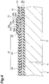
FIG. 4 is a cross-sectional view taken along a line IV-IV ofFIG. 3 . -
FIG. 5 is a cross-sectional view taken along a line V-V ofFIG.3 . -
FIG. 6 is a cross-sectional view of a first connection part of an actuator device of a first modified example. -
FIG. 7 is a cross-sectional view of a first connection part of an actuator device of a second modified example. -
FIG. 8 is a partially enlarged view of an actuator device of a third modified example. - Hereinafter, an embodiment of the present disclosure will be described in detail with reference to the drawings. In the following description, the same reference numerals will be used for the same or corresponding components and a repetitive description will be omitted.
- As illustrated in
FIGS. 1 and2 , anactuator device 1 includes amirror 2, amagnetic field generator 3, aframe 4, asupport portion 5, amovable portion 6, a pair ofconnection portions 7, and a pair ofconnection portions 8. Theactuator device 1 is configured as an MEMS device which swings themirror 2 about each of a first axis X1 and a second axis X2 which are orthogonal to each other. Such anactuator device 1 is used in, for example, an optical switch or optical scanner. - The
mirror 2 is a light reflection film formed by a metal film. Themirror 2 has a circular shape in the plan view (when viewed from a direction orthogonal to a plane in which at least thesupport portion 5, themovable portion 6, and the pair ofconnection portions 7 are arranged). A metal material forming themirror 2 is, for example, aluminum (Al), gold (Au), or silver (Ag). - The
magnetic field generator 3 is a rectangular flat plate and includes a pair of main surfaces. Themagnetic field generator 3 applies a magnetic field to acoil 11 provided with thesupport portion 5 and acoil 12 provided with the movable portion 6 (thecoils magnetic field generator 3 is configured as, for example, a permanent magnet or the like. The array of the magnetic poles of themagnetic field generator 3 is, for example, a Halbach array. - The
frame 4 is a flat plate-shaped frame having a rectangular shape in the plan view. Theframe 4 is disposed on one main surface of themagnetic field generator 3. Theframe 4 supports thesupport portion 5, themovable portion 6, and themirror 2 via the pair ofconnection portions 7. Eachconnection portion 7 connects thesupport portion 5 to theframe 4 on the first axis X1 so that thesupport portion 5 is swingable about the first axis X1. That is, eachconnection portion 7 serves as a torsion bar. Eachconnection portion 7 is formed in an S-shape in the plan view in order to improve the strength and facilitate the adjustment of the torsion spring constant. - The
support portion 5 is a flat plate-shaped frame having a rectangular shape in the plan view and is located at the inside of theframe 4. Thesupport portion 5 is disposed to face one main surface of themagnetic field generator 3 and to be separate from one main surface of themagnetic field generator 3. Thesupport portion 5 supports themovable portion 6 and themirror 2 via the pair ofconnection portions 8. Eachconnection portion 8 connects themovable portion 6 to thesupport portion 5 on the second axis X2 so that themovable portion 6 is swingable about the second axis X2. That is, eachconnection portion 8 serves as a torsion bar. - As illustrated in
FIG. 3 , eachconnection portion 8 is a flat plate-shaped member having a substantially rectangular shape in the plan view and extends along the second axis X2. Anend 8a on the side of themovable portion 6 in eachconnection portion 8 increases in width as it approaches themovable portion 6. Here, the width of theconnection portion 8 means the length of theconnection portion 8 in a direction orthogonal to the second axis X2 in the plan view. When theconnection portion 8 increases in width in at least one end and is connected to thesupport portion 5 or themovable portion 6, theconnection portion 8 is, for example, a region until the width becomes 1.5 times a minimum width W0. InFIG. 3 , a boundary B between theconnection portion 8 and thesupport portion 5 and a boundary B between theconnection portion 8 and themovable portion 6 are indicated by a two-dotted chain line. Theconnection portion 8 may be a region where the stress applied during the swing of themovable portion 6 with respect to thesupport portion 5 is larger than2/3 times the maximum stress. - As illustrated in
FIGS. 1 and2 , themovable portion 6 is a flat plate-shaped frame having a rectangular shape in the plan view and is located at the inside of thesupport portion 5. Themovable portion 6 is disposed to face one main surface of themagnetic field generator 3 and to be separate from one main surface of themagnetic field generator 3. Anarrangement portion 9 having a circular shape in the plan view is provided at the inside of themovable portion 6. Themirror 2 is disposed on thearrangement portion 9. That is, themirror 2 is provided with themovable portion 6. Theframe 4, thesupport portion 5, themovable portion 6, the pair ofconnection portions 7, and the pair ofconnection portions 8 are integrally formed of, for example, silicon (Si). - The
actuator device 1 further includes, as illustrated inFIG. 2 , thecoil 11 provided with thesupport portion 5 and thecoil 12 provided with themovable portion 6. Thecoil 11 is buried in thesupport portion 5 and thecoil 12 is buried in themovable portion 6. Each of thecoils FIG. 2 , each wiring is indicated by a solid line in order to facilitate understanding, but the wirings like thecoils insulation layer 52 and/or aninsulation layer 53 which will be described later. - The
coil 11 is wound a plurality of turns in a spiral shape in the plan view. One end of awiring 14a is electrically connected to an inner end of thecoil 11. One end of awiring 14b is electrically connected to an outer end of thecoil 11. Each of thewirings wirings connection portion 7 and extends from thesupport portion 5 to theframe 4. The other end of thewiring 14a is electrically connected to anelectrode 15a provided with thesupport portion 5 and the other end of thewiring 14b is electrically connected to anelectrode 15b provided with thesupport portion 5. Each of theelectrodes wiring 14a three-dimensionally intersects thecoil 11 to pass over thecoil 11. - The
coil 12 is wound a plurality of turns in a spiral shape in the plan view. One end of awiring 16a is electrically connected to an inner end of thecoil 12. One end of awiring 16b is electrically connected to an outer end of thecoil 12. Each of thewirings connection portions 8, thesupport portion 5, and theother connection portion 7 and extends from themovable portion 6 to theframe 4. The other end of thewiring 16a is electrically connected to anelectrode 17a provided with thesupport portion 5 and the other end of thewiring 16b is electrically connected to anelectrode 17b provided with thesupport portion 5. Each of theelectrodes wiring 16a three-dimensionally intersects thecoil 12 to pass over thecoil 12. - Each of the
wirings first wiring 21 provided on eachconnection portion 8, asecond wiring 31 provided on thesupport portion 5, and athird wiring 41 provided on themovable portion 6. Hereinafter, the configurations of thefirst wiring 21, thesecond wiring 31, and thethird wiring 41 in the vicinity of oneconnection portion 8 will be described with reference toFIGS. 3 ,4 , and5 . Because the configurations of thefirst wiring 21 and the like in the vicinity of theother connection portion 8 are the same as the configurations of thefirst wiring 21 and the like in the vicinity of oneconnection portion 8, a description thereof will be omitted. The insulation layer 52 (seeFIGS. 4 and5 ) is omitted inFIG. 3 . - The
first wiring 21 is formed of a first metal material. Thefirst wiring 21 is provided over thesupport portion 5, theconnection portion 8, and themovable portion 6. Thefirst wiring 21 includes afirst portion 22, asecond portion 23, and athird portion 24. Thefirst portion 22 extends along the second axis X2 on thesupport portion 5, theconnection portion 8, and themovable portion 6. Thesecond portion 23 extends from an end on the side of thesupport portion 5 in thefirst portion 22 to theother connection portion 7 on thesupport portion 5. Thethird portion 24 extends from an end on the side of themovable portion 6 in thefirst portion 22 to the oneconnection portion 7 on themovable portion 6. The extension direction of thefirst portion 22 and the extension direction of thesecond portion 23 are orthogonal to each other and the extension direction of thefirst portion 22 and the extension direction of thethird portion 24 are orthogonal to each other. - The
first wiring 21 is electrically connected to thesecond wiring 31 in afirst connection part 25 located at an end on thesupport portion 5. Thefirst wiring 21 is electrically connected to thethird wiring 41 in asecond connection part 26 located at an end on themovable portion 6. Thefirst connection part 25 is separate from the second axis X2 by a predetermined distance D1. The distance D1 is larger than 1/2 times the minimum width W0 of theconnection portion 8. Thesecond connection part 26 is separate from the second axis X2 by a predetermined distance D2. The distance D2 is larger than 1/2 times the minimum width W0 of theconnection portion 8. Thefirst portion 22, thesecond portion 23, and thethird portion 24 have the same width. The width W1 of thefirst wiring 21 is 1/2 times or more the minimum width W0 of theconnection portion 8 and is 2/3 times or more in this example. Here, the width W1 of thefirst wiring 21 indicates the length of thefirst wiring 21 in a direction orthogonal to the extension direction of thefirst wiring 21 in the plan view. In thefirst portion 22, the width indicates the length of thefirst portion 22 in a direction orthogonal to the second axis X2 in the plan view. Additionally, the width W1 of thefirst wiring 21 is, for example, about 50 to 100 µm. - The
second wiring 31 is formed of a second metal material. One end of thesecond wiring 31 is electrically connected to thefirst wiring 21. The other end of thesecond wiring 31 is electrically connected to theelectrode 17a. Awide portion 32 which has a width larger than that of the other portion is provided at one end of thesecond wiring 31. Thesecond wiring 31 is electrically connected to thefirst connection part 25 of thefirst wiring 21 in thewide portion 32. - The
third wiring 41 is formed of a third metal material. One end of thethird wiring 41 is electrically connected to thefirst wiring 21. The other end of thethird wiring 41 is electrically connected to thecoil 12. Awide portion 42 having a width larger than that of the other portion is provided at one end of thethird wiring 41. Thethird wiring 41 is electrically connected to thesecond connection part 26 of thefirst wiring 21 in thewide portion 42. - The rigidity of the first metal material forming the
first wiring 21 is higher than the rigidity of the second metal material forming thesecond wiring 31. The rigidity of the first metal material forming thefirst wiring 21 is higher than the rigidity of the third metal material forming thethird wiring 41. In other words, the rigidity of the second metal material forming thesecond wiring 31 is lower than the rigidity of the first metal material forming thefirst wiring 21. The rigidity of the third metal material forming thethird wiring 41 is lower than the rigidity of the first metal material forming thefirst wiring 21. Examples of a combination of the first metal material and the second metal material are a combination of tungsten (W) (the first metal material) and aluminum (the second metal material), a combination of tungsten (the first metal material) and copper (the second metal material), a combination of tungsten (the first metal material) and gold (the second metal material), and the like. Examples of a combination of the first metal material and the third metal material are a combination of tungsten (W) (the first metal material) and aluminum (the third metal material), a combination of tungsten (the first metal material) and copper (the third metal material), a combination of tungsten (the first metal material) and gold (the third metal material), and the like. The first metal material may be an aluminum alloy (AL-Cu or the like), nickel (Ni), platinum (Pt), or the like. - In the
actuator device 1, the width W1 of thefirst wiring 21 is larger than each of the width W2 of thesecond wiring 31 and the width W3 of thethird wiring 41. The thickness of thefirst wiring 21 is the same as each of the thickness of thesecond wiring 31 and the thickness of thethird wiring 41. Thus, the cross-sectional area of thefirst wiring 21 is larger than each of the cross-sectional area of thesecond wiring 31 and the cross-sectional area of thethird wiring 41. Here, the width W2 of thesecond wiring 31 means the length of the second wiring 31 (excluding the wide portion 32) in a direction orthogonal to the extension direction of thesecond wiring 31 in the plan view. The width W3 of thethird wiring 41 means the length of the third wiring 41 (excluding the wide portion 42) in a direction orthogonal to the extension direction of thethird wiring 41 in the plan view. The cross-sectional area of thefirst wiring 21 means an area of a cross-section orthogonal to the extension direction of thefirst wiring 21. The cross-sectional area of thesecond wiring 31 means an area of a cross-section orthogonal to the extension direction of thesecond wiring 31. The cross-sectional area of thethird wiring 41 means an area of a cross-section orthogonal to the extension direction of thethird wiring 41. Additionally, the width of thesecond wiring 31 is, for example, about 5 to 10 µm. - As illustrated in
FIG. 4 , theactuator device 1 further includes insulation layers 51, 52, and 53. Each of the insulation layers 51, 52, and 53 is, for example, a silicon oxide film (SiO2). - The
insulation layer 51 is provided on the surfaces of theframe 4, thesupport portion 5, themovable portion 6, the pair ofconnection portions 7, and the pair ofconnection portions 8. Thefirst wiring 21 is provided on theinsulation layer 51. That is, thefirst wiring 21 is provided on thesupport portion 5 via theinsulation layer 51. - The
insulation layer 52 is provided on theinsulation layer 51 so as to cover thefirst wiring 21. Theinsulation layer 52 is provided over theframe 4, thesupport portion 5, themovable portion 6, the pair ofconnection portions 7, and the pair ofconnection portions 8. Theinsulation layer 52 includes afirst opening 52a which exposes asurface 25a opposite to thesupport portion 5 in thefirst connection part 25. Thefirst opening 52a is a hole having a circular shape in the plan view. Thefirst opening 52a is separate from acorner 25b of thefirst connection part 25 by a predetermined distance. Theinsulation layer 52 covers thecorner 25b of thefirst connection part 25. A region 53d corresponding to thecorner 25b in the surface opposite to thesupport portion 5 in theinsulation layer 52 is curved in a convex shape toward the opposite side of thesupport portion 5. Here, thecorner 25b of thefirst connection part 25 means a portion along an outer edge of thesurface 25a in the first connection part 25 (i.e. a portion in which at least two surfaces of thefirst connection part 25 intersect each other). - The
second wiring 31 is provided on theinsulation layer 52. That is, thesecond wiring 31 is provided on thesupport portion 5 via the insulation layers 51 and 52. Thewide portion 32 of thesecond wiring 31 runs on thefirst connection part 25 to cover thefirst opening 52a. Apart 32a of thewide portion 32 is disposed inside thefirst opening 52a and is connected to thesurface 25a of thefirst connection part 25 in thefirst opening 52a. Thewide portion 32 includes aconcave portion 32b at a position corresponding to thefirst opening 52a in the surface opposite to thesupport portion 5. Theconcave portion 32b is formed such that apart 32a of thewide portion 32 enters thefirst opening 52a at the time of forming thesecond wiring 31. - An electric connection structure between the
first wiring 21 and thethird wiring 41 is the same as the above-described electric connection structure between thefirst wiring 21 and thesecond wiring 31. That is, as illustrated inFIG. 3 , theinsulation layer 52 includes asecond opening 52b which exposes asurface 26a opposite to themovable portion 6 in thesecond connection part 26. Thesecond opening 52b is a hole having a circular shape in the plan view. Thesecond opening 52b is separate from acorner 26b of thesecond connection part 26 by a predetermined distance. Theinsulation layer 52 covers thecorner 26b of thesecond connection part 26. A region corresponding to thecorner 26b in the surface opposite to themovable portion 6 in theinsulation layer 52 is curved in a convex shape toward the opposite side to themovable portion 6. Here, thecorner 26b of thesecond connection part 26 means a portion along an outer edge of thesurface 26a of the second connection part 26 (i.e. a portion in which at least two surfaces of thesecond connection part 26 intersect each other). - The
third wiring 41 is provided on theinsulation layer 52. That is, thethird wiring 41 is provided on themovable portion 6 via the insulation layers 51 and 52. Thewide portion 42 of thethird wiring 41 runs on thesecond connection part 26 to cover thesecond opening 52b. A part of thewide portion 42 is disposed inside thesecond opening 52b and is connected to thesurface 26a of thesecond connection part 26 in thesecond opening 52b. Thewide portion 42 includes a concave portion at a position corresponding to thesecond opening 52b in the surface opposite to thesupport portion 5. The concave portion is formed such that a part of thewide portion 42 enters thesecond opening 52b at the time of forming thethird wiring 41. - The
insulation layer 53 is provided on theinsulation layer 52 to cover thesecond wiring 31 and thethird wiring 41. Theinsulation layer 53 is provided over theframe 4, thesupport portion 5, themovable portion 6, the pair ofconnection portions 7, and the pair ofconnection portions 8. Theinsulation layer 53 includes aconcave portion 53a at a position corresponding to thefirst opening 52a in the surface opposite to thesupport portion 5. Theconcave portion 53a is formed such that a part of theinsulation layer 53 enters theconcave portion 32b at the time of forming theinsulation layer 53. Theinsulation layer 53 includes a concave portion at a position corresponding to thesecond opening 52b in the surface opposite to thesupport portion 5. The concave portion of theinsulation layer 53 is formed such that a part of theinsulation layer 53 enters the concave portion of thewide portion 42 at the time of forming theinsulation layer 53. - As illustrated in
FIG. 5 , themovable portion 6 is provided with agroove portion 55 having a shape corresponding to thecoil 12. An inner surface of thegroove portion 55 is provided with theinsulation layer 51. Aseed layer 56 is provided on theinsulation layer 51 inside thegroove portion 55. Theseed layer 56 is formed of, for example, titanium nitride (TiN). Thecoil 12 is disposed inside thegroove portion 55 via theinsulation layer 51 and theseed layer 56. Thecoil 12 is formed by burying, for example, a metal material such as copper in thegroove portion 55 according to, for example, a damascene method. Theinsulation layer 52 is provided to cover thecoil 12 disposed inside thegroove portion 55. Thethird wiring 41 is electrically connected to thecoil 12 via an opening provided with theinsulation layer 52 so that an inner end of thecoil 12 is exposed. - A
groove portion 13 is formed along the boundary between theseed layer 56 and the surface on the side of theinsulation layer 52 in thecoil 12 at the time of forming thecoil 12. Theinsulation layer 52 includes agroove portion 52c at a position corresponding to thegroove portion 13 in the surface opposite to themovable portion 6. Thegroove portion 52c is formed such that a part of theinsulation layer 52 enters thegroove portion 13 at the time of forming theinsulation layer 52. Thethird wiring 41 includes agroove portion 41a at a position corresponding to the groove portion 12a in the surface opposite to themovable portion 6. Thegroove portion 41a is formed such that a part of thethird wiring 41 enters thegroove portion 52c at the time of forming thethird wiring 41. Theinsulation layer 53 includes agroove portion 53b at a position corresponding to the groove portion 12a in the surface opposite to themovable portion 6. Thegroove portion 53b is formed such that a part of theinsulation layer 53 enters thegroove portion 41a at the time of forming theinsulation layer 53. - In the
actuator device 1, when a current flows to thecoil 11, a Lorentz force is generated in a predetermined direction by electrons flowing in thecoil 11 by a magnetic field generated by themagnetic field generator 3. Accordingly, thecoil 11 receives a force in a predetermined direction. For this reason, it is possible to swing thesupport portion 5 about the first axis X1 by controlling the direction or the magnitude of the current flowing in thecoil 11. Similarly, it is possible to swing themovable portion 6 about the second axis X2 by controlling the direction or the magnitude of the current flowing in thecoil 12. Thus, it is possible to swing themirror 2 about each of the first axis X1 and the second axis X2 which are orthogonal to each other by controlling the direction or the magnitude of the current flowing in thecoil 11 and thecoil 12. Further, it is possible to swing themovable portion 6 at a high speed at the resonance frequency level by applying a current having a frequency corresponding to the resonance frequency of themovable portion 6 to thecoil 12. - In the above-described
actuator device 1, the rigidity of the first metal material forming thefirst wiring 21 provided on theconnection portion 8 is higher than the rigidity of the second metal material forming thesecond wiring 31 provided on thesupport portion 5. Accordingly, deterioration of thefirst wiring 21 provided on theconnection portion 8 is suppressed. Also, it is possible to suppress the deformation (curving or the like) of thesupport portion 5 caused when the entire wiring provided on theconnection portion 8 and thesupport portion 5 is formed of the first metal material having high rigidity. Further, thefirst wiring 21 and thesecond wiring 31 are connected to each other at thefirst connection part 25 located on thesupport portion 5. Accordingly, stress applied to thefirst connection part 25 is reduced and deterioration of thefirst connection part 25 is suppressed. Further, in theactuator device 1, thecorner 25b of thefirst connection part 25 is covered by theinsulation layer 52 and thefirst wiring 21 and thesecond wiring 31 are connected to each other in thesurface 25a opposite to thesupport portion 5 in thefirst connection part 25 exposed by thefirst opening 52a of theinsulation layer 52. Accordingly, because stress applied from thefirst wiring 21 to thesecond wiring 31 is reduced by theinsulation layer 52, deterioration of thesecond wiring 31 formed of the second metal material of which the rigidity is lower than that of the first metal material is suppressed. Thus, according to theactuator device 1, it is possible to suppress deterioration of thewirings connection portion 8 and thesupport portion 5. Further, because thefirst wiring 21 and thesecond wiring 31 are directly connected to each other, it is possible to reduce the resistance of thewirings connection portion 8 and thesupport portion 5. - In the
actuator device 1, thefirst connection part 25 is separate from the second axis X2 by a predetermined distance D. Accordingly, it is possible to reduce stress applied to thefirst connection part 25 while securing a region for providing another configuration (for example, the coil 11) on thesupport portion 5. That is, it is possible to secure a region for providing another configuration on thesupport portion 5 compared to a case in which stress applied to thefirst connection part 25 is reduced by securing a distance along the second axis X2 between thefirst connection part 25 and theconnection portion 8. - In the
actuator device 1, the distance D is larger than 1/2 times the minimum width W0 of theconnection portion 8. Accordingly, it is possible to further reduce stress applied to thefirst connection part 25 while securing a region for providing another configuration on thesupport portion 5. - In the
actuator device 1, the cross-sectional area of thefirst wiring 21 is larger than the cross-sectional area of thesecond wiring 31. Accordingly, it is possible to suppress an increase in resistance value of thefirst wiring 21 even when the resistivity of the first metal material forming thefirst wiring 21 is higher than the resistivity of the second metal material forming thesecond wiring 31. - In the
actuator device 1, the width of thefirst wiring 21 is larger than the width of thesecond wiring 31. Accordingly, it is possible to suppress an increase in resistance value of thefirst wiring 21 by securing the cross-sectional area of thefirst wiring 21 while suppressing the torsion of theconnection portion 8 from being obstructed. - In the
actuator device 1, thefirst opening 52a is separate from thecorner 25b of thefirst connection part 25. Accordingly, it is possible to reliably reduce stress applied from thefirst wiring 21 to thesecond wiring 31. - In the
actuator device 1, the region 53d corresponding to thecorner 25b in the surface opposite to thesupport portion 5 in theinsulation layer 52 is curved in a convex shape toward the opposite side to the support portion. Accordingly, it is possible to further reduce stress applied from thefirst wiring 21 to thesecond wiring 31. - In the
actuator device 1, the rigidity of the first metal material forming thefirst wiring 21 provided on theconnection portion 8 is higher than the rigidity of the third metal material forming thethird wiring 41 provided on themovable portion 6. Further, thefirst wiring 21 and thethird wiring 41 are connected to each other in thesecond connection part 26 located on themovable portion 6. Further, thecorner 26b of thesecond connection part 26 is covered by theinsulation layer 52 and thefirst wiring 21 and thethird wiring 41 are connected to each other in thesurface 26a opposite to themovable portion 6 in thesecond connection part 26 exposed by thesecond opening 52b of theinsulation layer 52. Thus, it is possible to suppress deterioration of thewirings connection portion 8 and themovable portion 6. - The
actuator device 1 further includes theframe 4 which supports thesupport portion 5 and themovable portion 6 and thesupport portion 5 is connected to theframe 4 to be swingable about the first axis X1 orthogonal to the second axis X2. Accordingly, it is possible to swing themovable portion 6 about each of two orthogonal axes. - The
actuator device 1 further includes themirror 2 provided with themovable portion 6. Accordingly, it is possible to use themirror 2 for the light scanning or the like by swinging the mirror about each of the first axis X1 and the second axis X2. - In the
actuator device 1, thesecond wiring 31 is connected to thesurface 25a opposite to thesupport portion 5 in thefirst connection part 25 located on thesupport portion 5 in thefirst wiring 21. Accordingly, because the stress applied from thefirst wiring 21 to thesecond wiring 31 is released to the opposite side to thesupport portion 5, it is possible to suppress deterioration of thesecond wiring 31 formed of the second metal material having rigidity lower than that of the first metal material. That is, it is possible to prevent a problem in which the stress applied from thesecond wiring 31 to thefirst wiring 21 and the reaction force from thesupport portion 5 intensively act on the end of thesecond wiring 31, which happens in a case in which the end of thesecond wiring 31 is interposed between thefirst wiring 21 and thesupport portion 5. Also with this configuration, according to theactuator device 1, it is possible to suppress deterioration of thewirings connection portion 8 and thesupport portion 5. - While the embodiment of the present disclosure has been described above, an embodiment of the present disclosure is not limited to the above-described embodiment. For example, the
second wiring 31 may be electrically connected to thefirst wiring 21 in thefirst connection part 33 located at the end on thesupport portion 5 similarly to a first modified example illustrated inFIG. 6 . In the first modified example, thesecond wiring 31 is provided on theinsulation layer 51. Theinsulation layer 52 is provided on theinsulation layer 51 to cover thesecond wiring 31. Theinsulation layer 52 includes thefirst opening 52a which exposes asurface 33a opposite to thesupport portion 5 in thefirst connection part 33. Theinsulation layer 52 includes acorner 33b of thefirst connection part 33. The region 53d corresponding to thecorner 25b in the surface opposite to thesupport portion 5 in theinsulation layer 52 is curved in a convex shape toward the opposite side to thesupport portion 5. Thefirst wiring 21 is provided on theinsulation layer 52. The end of thesecond portion 23 in thefirst wiring 21 runs on thefirst connection part 33 to cover thefirst opening 52a. Apart 23a of thesecond portion 23 is disposed inside thefirst opening 52a and is connected to thesurface 33a of thefirst connection part 33 in thefirst opening 52a. Also in the first modified example, it is possible to suppress deterioration of thewirings connection portion 8 and thesupport portion 5 similarly to the above-described embodiment. Further, thethird wiring 41 may be electrically connected to thefirst wiring 21 in thesecond connection part 26 located at the end on themovable portion 6 similarly to the first modified example. - Similarly to a second modified example illustrated in
FIG. 7 , adiffusion layer 58 may be provided instead of theinsulation layer 51. Thediffusion layer 58 is provided with a region contacting thefirst wiring 21 on the surfaces of thesupport portion 5, themovable portion 6, and the pair ofconnection portions 8. Thediffusion layer 58 is, for example, a diffusion region formed by diffusing a p-type impurity on a surface of an n-type silicon substrate. Also in the second modified example, it is possible to suppress deterioration of thewirings connection portion 8 and thesupport portion 5 similarly to the above-described embodiment. Further, according to the second modified example, because thediffusion layer 58 serves as a part of thefirst wiring 21, it is possible to reduce the resistance of thewirings connection portion 8 and thesupport portion 5 while securing the insulation at thediffusion layer 58. Further, when the first metal material is tungsten, thefirst wiring 21 can be stably provided on theconnection portion 8 because tungsten easily adheres to thediffusion layer 58. - Similarly to a third modified example illustrated in
FIG. 8 , anend 8b on the side of thesupport portion 5 in eachconnection portion 8 may increase in width as it approaches thesupport portion 5. InFIG. 8 , a boundary B between theconnection portion 8 and thesupport portion 5 and a boundary B between theconnection portion 8 and themovable portion 6 are indicated by a two-dotted chain line. Also in the third modified example, it is possible to suppress deterioration of thewirings connection portion 8 and thesupport portion 5 similarly to the above-described embodiment. - In the above-described embodiment, the
first wiring 21, thesecond wiring 31, and thethird wiring 41 may be provided with theconnection portion 7 as well as theconnection portion 8. In this case, thefirst wiring 21 is provided on theconnection portion 7 and thesecond wiring 31 is provided on theframe 4 to be electrically connected to theelectrodes electrodes third wiring 41 is provided on thesupport portion 5 to be electrically connected to thecoil 11 or thesecond wiring 31 of the above-described embodiment. Theconnection portion 7 may have a linear shape. Theconnection portion 8 may have an arbitrary shape as long as themovable portion 6 is connected to thesupport portion 5 on the second axis X2 so that themovable portion 6 is swingable about the second axis X2. - In the above-described embodiment, the
insulation layer 52 is provided over theframe 4, thesupport portion 5, themovable portion 6, the pair ofconnection portions 7, and the pair ofconnection portions 8, but may be provided at least so as to be interposed between at least thefirst wiring 21 and thesecond wiring 31 or thethird wiring 41. The shapes of thefirst opening 52a and thesecond opening 52b are not limited to circular shapes. Thefirst opening 52a and thesecond opening 52b may have, for example, a rectangular shape, a rhombic shape, or the like. Further, thefirst opening 52a and thesecond opening 52b may have, for example, a notch shape opened to the extension direction of thesecond portion 23 or thethird portion 24. - A part of the
first opening 52a may contact thecorner 25b of thefirst connection part 25. Also with this configuration, because thecorner 25b is covered by theinsulation layer 52, it is possible to reduce stress applied from thefirst wiring 21 to thesecond wiring 31 similarly to the above-described embodiment. A part of thesecond opening 52b may contact thecorner 26b of thesecond connection part 26. Also with this configuration, because thecorner 26b is covered by theinsulation layer 52, it is possible to reduce stress applied from thefirst wiring 21 to thesecond wiring 31 similarly to the above-described embodiment. A region corresponding to thecorner 25b in the surface opposite to thesupport portion 5 in theinsulation layer 52 may not be curved in a convex shape and may be curved in, for example, a plane shape. Also with this configuration, it is possible to reduce stress applied from thefirst wiring 21 to thesecond wiring 31 similarly to the above-described embodiment. A region corresponding to thecorner 26b in the surface opposite to themovable portion 6 in theinsulation layer 52 may not be curved in a convex shape and may be curved in, for example, a plane shape. Also with this configuration, it is possible to reduce stress applied from thefirst wiring 21 to thesecond wiring 31 similarly to the above-described embodiment. - The
first connection part 25 may be separate from the second axis X2 by a predetermined distance and may not be separated therefrom by the distance D1 larger than 1/2 times the minimum width W0 of theconnection portion 8. Similarly, thesecond connection part 26 may be separate from the second axis X2 by a predetermined distance and may not be separated therefrom by the distance D2 larger than 1/2 times the minimum width W0 of theconnection portion 8. Thesecond wiring 31 may not be provided with thewide portion 32 and thethird wiring 41 may not be provided with thewide portion 42. Thethird wiring 41 may be electrically connected to thecoil 12 via another member formed of a metal material. - In the
first wiring 21, thefirst portion 22 and thesecond portion 23 or thethird portion 24 may intersect each other at an angle other than the perpendicular direction. Alternatively, the wholefirst wiring 21 may straightly extend along the extension direction of the connection portion. In this case, thefirst connection part 25 is located on the second axis X2. Thefirst portion 22, thesecond portion 23, and thethird portion 24 may not have the same width. In this case, the width of thefirst wiring 21 means the minimum width or the maximum width of thefirst portion 22, thesecond portion 23, and thethird portion 24. - The cross-sectional area of the
first wiring 21 may be larger than the cross-sectional area of thesecond wiring 31 and the width W1 of thefirst wiring 21 may be smaller than the width W2 of thesecond wiring 31. For example, the thickness of thefirst wiring 21 may be larger than the thickness of thesecond wiring 31, and thus the cross-sectional area of thefirst wiring 21 may be larger than the cross-sectional area of thesecond wiring 31. Here, the above-described embodiment is preferable in that the torsion of theconnection portion 8 can be prevented and the manufacturing can be facilitated. Similarly, the cross-sectional area of thefirst wiring 21 may be larger than the cross-sectional area of thethird wiring 41 and the width W1 of thefirst wiring 21 may be smaller than the width W3 of thethird wiring 41. The cross-sectional area of thefirst wiring 21 may be equal to or smaller than the cross-sectional area of thesecond wiring 31 or thethird wiring 41. - The
actuator device 1 may be used to drive an object other than themirror 2. The shape of themirror 2 is not limited to the circular shape. Themirror 2 may have, for example, a rectangular shape, a rhombic shape, or the like. In the above-described embodiment, the swinging (driving) of themirror 2 is performed by an electromagnetic force, but may be performed by, for example, a piezoelectric element. In this case, a wiring for applying a voltage to the piezoelectric element is provided instead of thecoils magnetic field generator 3 may be omitted. - The first axis X1 and the second axis X2 may not be orthogonal to each other and may intersect each other. The
actuator device 1 may swing only about the second axis X2. In this case, theframe 4 and theconnection portion 7 may be omitted and an electrode to be electrically connected to a control circuit or the like may be provided with thesupport portion 5. Theconnection portion 8 may be a region where the width is smaller than 2 times the minimum width W0. Alternatively, theconnection portion 8 may be a region where the stress applied during the swing of themovable portion 6 with respect to thesupport portion 5 is larger than 1/2 times the maximum stress. - In the above-described embodiment, the
insulation layer 52 covers theentire corner 25b of thefirst connection part 25, but may cover at least a part of thecorner 25b. For example, theinsulation layer 52 may cover at least a portion of thecorner 25b in thefirst connection part 25 where thesurface 25a opposite to thesupport portion 5 intersects the surface (in the above-described embodiment, the surface on the side of the other connection portion 7) on the side to which thesecond wiring 31 is drawn out. Even when theinsulation layer 52 covers only a portion in which thesurface 25a opposite to thesupport portion 5 intersects the surface in which thesecond wiring 31 in thefirst connection part 25 is drawn in thecorner 25b, it is possible to suppress deterioration of thewirings connection portion 8 and thesupport portion 5 similarly to the above-described embodiment. Thesecond wiring 31 may be drawn along the second axis X2 from, for example, thefirst connection part 25. Similarly to thecorner 26b of thesecond connection part 26, theinsulation layer 52 may cover at least a part of thecorner 26b. - E1: An actuator device comprising: a support portion; a movable portion; a connection portion which connects the movable portion to the support portion on a predetermined axis so that the movable portion is swingable about the axis; a first wiring which is provided on the connection portion; a second wiring which is provided on the support portion; and an insulation layer which includes a first opening exposing a surface opposite to the support portion in a first connection part located on the support portion in one wiring of the first wiring and the second wiring and covers a corner of the first connection part, wherein rigidity of a first metal material forming the first wiring is higher than rigidity of a second metal material forming the second wiring, and wherein the other wiring of the first wiring and the second wiring is connected to the surface of the first connection part in the first opening.
- E2: The actuator device according to E1, wherein the first connection part is separate from the axis by a predetermined distance.
- E3: The actuator device according to E2, wherein the distance is larger than 1/2 times a minimum width of the connection portion.
- E4: The actuator device according to any one of E1 to E3, wherein a cross-sectional area of the first wiring is larger than a cross-sectional area of the second wiring.
- E5: The actuator device according to E4, wherein a width of the first wiring is larger than a width of the second wiring.
- E6: The actuator device according to any one of E1 to E5, wherein the first opening is separate from the corner of the first connection part.
- E7: The actuator device according to any one of E1 to E6, wherein a region corresponding to the corner of the first connection part in a surface opposite to the support portion in the insulation layer is curved in a convex shape toward the opposite side to the support portion.
- E8: The actuator device according to any one of E1 to E7, further comprising: a coil which is provided with the movable portion; a magnetic field generator which applies a magnetic field to the coil; and a third wiring which is provided on the movable portion and is electrically connected to the coil, wherein the insulation layer includes a second opening exposing a surface opposite to the movable portion in a second connection part located on the movable portion in one wiring of the first wiring and the third wiring and covers a corner of the second connection part, wherein rigidity of the first metal material is higher than rigidity of a third metal material forming the third wiring, and wherein the other wiring of the first wiring and the third wiring is connected to the surface of the second connection part in the second opening.
- E9: The actuator device according to any one of E1 to E8, further comprising: a frame which supports the support portion and the movable portion, wherein the support portion is connected to the frame so as to be swingable about an axis intersecting the axis.
- E10: The actuator device according to any one of E1 to E9, further comprising: a mirror which is provided with the movable portion.
- 1 ... actuator device, 2 ... mirror, 3 ... magnetic field generator, 4 ... frame, 5 ... support portion, 6 ... movable portion, 8 ... connection portion, 12 ... coil, 21 ... first wiring, 25, 33 ... first connection part, 25a, 33a ... surface, 25b, 33b ... corner, 26 ... second connection part, 26a ... surface, 26b ... corner, 31 ... second wiring, 41 ... third wiring, 52 ... insulation layer, 52a ... first opening, 52b ... second opening.
Claims (11)
- An actuator device comprising:a support portion;a movable portion;a connection portion which connects the movable portion to the support portion on a predetermined axis so that the movable portion is swingable about the axis;a first wiring which is provided to the connection portion;a second wiring which is provided to the movable portion and includes a coil; anda first insulation layer which includes a first opening exposing a surface opposite to the movable portion in a first connection part located at the movable portion in one wiring of the first wiring and the second wiring,wherein rigidity of a first metal material forming the first wiring is higher than rigidity of a second metal material forming the second wiring, wherein the other wiring of the first wiring and the second wiring is connected to the surface of the first connection part in the first opening,wherein the first wiring includes a first portion which extends along the axis at the support portion, the connection portion, and the movable portion and a second portion which extends from an end of the first portion on the side of the movable portion along a direction intersecting the axis at the movable portion, andwherein the second wiring is electrically connected to the first wiring at the second portion of the first wiring.
- The actuator device according to claim 1,
wherein the first connection part is separate from the axis by a predetermined distance and the distance is larger than 1/2 times a minimum width of the connection portion. - The actuator device according to claim 1 or 2,
wherein a cross-sectional area of the first wiring is larger than a cross-sectional area of the second wiring. - The actuator device according to any one of claims 1 to 3,
wherein a width of the first wiring is larger than a width of the second wiring. - The actuator device according to any one of claims 1 to 4,
wherein the first opening is separate from a corner of the first connection part. - The actuator device according to any one of claims 1 to 5, wherein the one wiring of the first wiring and the second wiring is the first wiring and the other wiring of the first wiring and the second wiring is the second wiring.
- The actuator device according to any one of claims 1 to 5, wherein the one wiring of the first wiring and the second wiring is the second wiring and the other wiring of the first wiring and the second wiring is the first wiring.
- The actuator device according to any one of claims 1 to 7, wherein an end of the second wiring is provided with a wide portion having a width larger than that of a portion other than the wide portion in the second wiring and the second wiring is electrically connected to the first wiring at the wide portion.
- The actuator device according to any one of claims 1 to 8, further comprising:a second insulation layer which covers the other wiring of the first wiring and the second wiring and the first insulation layer,wherein a region corresponding to a corner of the other wiring of the first wiring and the second wiring in a surface opposite to the movable portion in the second insulation layer is curved in a convex shape toward the opposite side to the movable portion.
- The actuator device according to any one of claims 1 to 9,wherein the movable portion includes a frame portion connected to the connection portion and an arrangement portion disposed inside the frame portion, andwherein a mirror is disposed at the arrangement portion and a coil is provided at the frame portion.
- The actuator device according to any one of claims 1 to 10, further comprising:a frame which supports the support portion and the movable portion,wherein the support portion is connected to the frame so as to be swingable about an axis intersecting the axis.
Priority Applications (1)
| Application Number | Priority Date | Filing Date | Title |
|---|---|---|---|
| EP25197043.0A EP4628963A3 (en) | 2016-01-21 | 2016-12-22 | Actuator device |
Applications Claiming Priority (3)
| Application Number | Priority Date | Filing Date | Title |
|---|---|---|---|
| JP2016009889A JP6696777B2 (en) | 2016-01-21 | 2016-01-21 | Actuator device |
| EP16886528.5A EP3407110B1 (en) | 2016-01-21 | 2016-12-22 | Actuator device |
| PCT/JP2016/088436 WO2017126289A1 (en) | 2016-01-21 | 2016-12-22 | Actuator device |
Related Parent Applications (2)
| Application Number | Title | Priority Date | Filing Date |
|---|---|---|---|
| EP16886528.5A Division EP3407110B1 (en) | 2016-01-21 | 2016-12-22 | Actuator device |
| EP16886528.5A Division-Into EP3407110B1 (en) | 2016-01-21 | 2016-12-22 | Actuator device |
Related Child Applications (2)
| Application Number | Title | Priority Date | Filing Date |
|---|---|---|---|
| EP25197043.0A Division-Into EP4628963A3 (en) | 2016-01-21 | 2016-12-22 | Actuator device |
| EP25197043.0A Division EP4628963A3 (en) | 2016-01-21 | 2016-12-22 | Actuator device |
Publications (2)
| Publication Number | Publication Date |
|---|---|
| EP4092476A1 true EP4092476A1 (en) | 2022-11-23 |
| EP4092476B1 EP4092476B1 (en) | 2025-10-15 |
Family
ID=59361654
Family Applications (3)
| Application Number | Title | Priority Date | Filing Date |
|---|---|---|---|
| EP16886528.5A Active EP3407110B1 (en) | 2016-01-21 | 2016-12-22 | Actuator device |
| EP22181244.9A Active EP4092476B1 (en) | 2016-01-21 | 2016-12-22 | Actuator device |
| EP25197043.0A Pending EP4628963A3 (en) | 2016-01-21 | 2016-12-22 | Actuator device |
Family Applications Before (1)
| Application Number | Title | Priority Date | Filing Date |
|---|---|---|---|
| EP16886528.5A Active EP3407110B1 (en) | 2016-01-21 | 2016-12-22 | Actuator device |
Family Applications After (1)
| Application Number | Title | Priority Date | Filing Date |
|---|---|---|---|
| EP25197043.0A Pending EP4628963A3 (en) | 2016-01-21 | 2016-12-22 | Actuator device |
Country Status (6)
| Country | Link |
|---|---|
| US (5) | US10589985B2 (en) |
| EP (3) | EP3407110B1 (en) |
| JP (1) | JP6696777B2 (en) |
| KR (1) | KR20180105114A (en) |
| CN (2) | CN112731652B (en) |
| WO (1) | WO2017126289A1 (en) |
Families Citing this family (20)
| Publication number | Priority date | Publication date | Assignee | Title |
|---|---|---|---|---|
| JP6696777B2 (en) * | 2016-01-21 | 2020-05-20 | 浜松ホトニクス株式会社 | Actuator device |
| JP7015653B2 (en) * | 2017-08-10 | 2022-02-03 | 浜松ホトニクス株式会社 | Optical module and manufacturing method of optical module |
| CN115051526A (en) * | 2017-12-01 | 2022-09-13 | 浜松光子学株式会社 | Actuator device |
| JP6585147B2 (en) * | 2017-12-01 | 2019-10-02 | 浜松ホトニクス株式会社 | Actuator device |
| JP1680755S (en) | 2018-05-01 | 2021-03-08 | ||
| JP1680385S (en) * | 2018-05-01 | 2021-03-01 | ||
| JP1625495S (en) * | 2018-05-01 | 2019-03-18 | ||
| JP1680388S (en) * | 2018-05-01 | 2021-03-01 | ||
| USD907085S1 (en) | 2018-05-01 | 2021-01-05 | Hamamatsu Photonics K.K. | Laser beam reflector |
| JP1680386S (en) * | 2018-05-01 | 2021-03-01 | ||
| JP1680387S (en) * | 2018-05-01 | 2021-03-01 | ||
| JP1625135S (en) * | 2018-05-01 | 2019-03-18 | ||
| USD903614S1 (en) | 2018-05-01 | 2020-12-01 | Hamamatsu Photonics K.K. | Laser beam reflector |
| JP1680507S (en) * | 2018-05-01 | 2021-03-08 | ||
| JP1639597S (en) * | 2018-05-01 | 2019-08-19 | ||
| US12187607B2 (en) | 2018-10-31 | 2025-01-07 | Hamamatsu Photonics K.K. | Method for manufacturing semiconductor substrate, method for manufacturing damascene wiring structure, semiconductor substrate, and damascene wiring structure |
| WO2020090931A1 (en) * | 2018-10-31 | 2020-05-07 | 浜松ホトニクス株式会社 | Damascene interconnect structure, actuator device, and method of manufacturing damascene interconnect structure |
| JP7313831B2 (en) | 2019-01-30 | 2023-07-25 | 浜松ホトニクス株式会社 | optical module |
| JP7587994B2 (en) * | 2021-01-28 | 2024-11-21 | 浜松ホトニクス株式会社 | Method for manufacturing an actuator device |
| EP4323647A1 (en) * | 2021-04-14 | 2024-02-21 | Cambridge Mechatronics Limited | Sma actuator assembly |
Citations (1)
| Publication number | Priority date | Publication date | Assignee | Title |
|---|---|---|---|---|
| US20100259806A1 (en) * | 2009-04-08 | 2010-10-14 | Microvision, Inc. | Fatigue Resistant MEMS Apparatus and System |
Family Cites Families (27)
| Publication number | Priority date | Publication date | Assignee | Title |
|---|---|---|---|---|
| JP3425814B2 (en) * | 1994-12-28 | 2003-07-14 | 日本信号株式会社 | Electromagnetic actuator and method of manufacturing the same |
| JP2001519726A (en) | 1997-04-01 | 2001-10-23 | クセロス・インク | Adjustment of dynamic characteristics of micromachined torsional vibrator |
| JP2001264677A (en) * | 2000-03-15 | 2001-09-26 | Olympus Optical Co Ltd | Scanning mirror |
| EP1408336A3 (en) | 2000-06-21 | 2005-06-29 | Input/Output, Inc. | Accelerometer with mass support springs having predetermined vibration modes |
| ATE355530T1 (en) * | 2001-07-26 | 2006-03-15 | Fraunhofer Ges Forschung | MICROMECHANICAL COMPONENT |
| US7091057B2 (en) * | 2003-12-19 | 2006-08-15 | Agency For Science, Technology And Research | Method of making a single-crystal-silicon 3D micromirror |
| JP4749790B2 (en) | 2004-08-20 | 2011-08-17 | 佐々木 実 | Micromirror device and manufacturing method thereof, angle measurement method of micromirror device, and micromirror device application apparatus |
| JP4385937B2 (en) * | 2004-12-15 | 2009-12-16 | セイコーエプソン株式会社 | Actuator |
| JP2007111847A (en) * | 2005-10-24 | 2007-05-10 | Olympus Corp | Actuator |
| JP2009251002A (en) * | 2008-04-01 | 2009-10-29 | Seiko Epson Corp | Actuator, image forming apparatus and method of manufacturing actuator |
| JP5634670B2 (en) * | 2008-10-20 | 2014-12-03 | 日本信号株式会社 | Planar actuator |
| JP2011186422A (en) * | 2010-02-10 | 2011-09-22 | Sanyo Electric Co Ltd | Beam irradiation device |
| US9036231B2 (en) * | 2010-10-20 | 2015-05-19 | Tiansheng ZHOU | Micro-electro-mechanical systems micromirrors and micromirror arrays |
| JP5842467B2 (en) | 2010-11-16 | 2016-01-13 | 株式会社リコー | Actuator device, protective cover for the actuator device, method for manufacturing the actuator, light deflection device using the actuator device, two-dimensional optical scanning device, and image projection device using the same |
| JP5834431B2 (en) | 2011-03-16 | 2015-12-24 | セイコーエプソン株式会社 | Actuator, actuator manufacturing method, optical scanner, and image forming apparatus |
| JP5681545B2 (en) * | 2011-03-29 | 2015-03-11 | 日本信号株式会社 | Planar electromagnetic actuator and manufacturing method thereof |
| JP2013035081A (en) * | 2011-08-04 | 2013-02-21 | Seiko Epson Corp | Actuator manufacturing method, actuator, optical scanner, and image forming apparatus |
| JP2013160892A (en) * | 2012-02-03 | 2013-08-19 | Funai Electric Co Ltd | Oscillation mirror element, method of manufacturing oscillation mirror element, and electronic equipment having projector function |
| CN105934698B (en) * | 2013-01-11 | 2019-04-16 | 英特尔公司 | mirror drive |
| JP2014182225A (en) * | 2013-03-18 | 2014-09-29 | Seiko Epson Corp | Optical scanner, actuator, image display device, and head-mounted display |
| KR101511145B1 (en) * | 2013-05-27 | 2015-04-10 | 주식회사 센플러스 | Electromagnetic actuator |
| JP6250323B2 (en) * | 2013-08-01 | 2017-12-20 | 浜松ホトニクス株式会社 | Mirror drive device |
| JP6253915B2 (en) * | 2013-08-01 | 2017-12-27 | 浜松ホトニクス株式会社 | Actuator device and mirror drive device |
| TWI538096B (en) * | 2013-12-31 | 2016-06-11 | 財團法人工業技術研究院 | Mems apparatus with pn-junction |
| EP3140563A4 (en) | 2014-05-06 | 2018-01-17 | Mems Drive Inc. | Low stiffness flexure |
| JP6696777B2 (en) * | 2016-01-21 | 2020-05-20 | 浜松ホトニクス株式会社 | Actuator device |
| CN115051526A (en) | 2017-12-01 | 2022-09-13 | 浜松光子学株式会社 | Actuator device |
-
2016
- 2016-01-21 JP JP2016009889A patent/JP6696777B2/en active Active
- 2016-12-22 KR KR1020187012576A patent/KR20180105114A/en not_active Withdrawn
- 2016-12-22 CN CN202011562410.7A patent/CN112731652B/en active Active
- 2016-12-22 US US16/070,562 patent/US10589985B2/en active Active
- 2016-12-22 EP EP16886528.5A patent/EP3407110B1/en active Active
- 2016-12-22 CN CN201680079450.1A patent/CN108474938B/en active Active
- 2016-12-22 EP EP22181244.9A patent/EP4092476B1/en active Active
- 2016-12-22 EP EP25197043.0A patent/EP4628963A3/en active Pending
- 2016-12-22 WO PCT/JP2016/088436 patent/WO2017126289A1/en not_active Ceased
-
2020
- 2020-02-13 US US16/789,795 patent/US11339050B2/en active Active
-
2022
- 2022-04-21 US US17/725,804 patent/US11952265B2/en active Active
-
2024
- 2024-02-20 US US18/581,466 patent/US12304806B2/en active Active
-
2025
- 2025-04-23 US US19/187,085 patent/US20250250160A1/en active Pending
Patent Citations (2)
| Publication number | Priority date | Publication date | Assignee | Title |
|---|---|---|---|---|
| US20100259806A1 (en) * | 2009-04-08 | 2010-10-14 | Microvision, Inc. | Fatigue Resistant MEMS Apparatus and System |
| US8218218B2 (en) | 2009-04-08 | 2012-07-10 | Microvision, Inc. | Fatigue resistant MEMS apparatus and system |
Also Published As
| Publication number | Publication date |
|---|---|
| US20240190699A1 (en) | 2024-06-13 |
| WO2017126289A1 (en) | 2017-07-27 |
| EP3407110B1 (en) | 2022-08-17 |
| US20190016589A1 (en) | 2019-01-17 |
| CN112731652B (en) | 2023-09-05 |
| EP3407110A4 (en) | 2019-09-25 |
| EP4092476B1 (en) | 2025-10-15 |
| EP4628963A3 (en) | 2025-12-24 |
| US11952265B2 (en) | 2024-04-09 |
| KR20180105114A (en) | 2018-09-27 |
| EP3407110A1 (en) | 2018-11-28 |
| CN112731652A (en) | 2021-04-30 |
| US20200180944A1 (en) | 2020-06-11 |
| CN108474938B (en) | 2021-01-19 |
| JP6696777B2 (en) | 2020-05-20 |
| US11339050B2 (en) | 2022-05-24 |
| JP2017129782A (en) | 2017-07-27 |
| CN108474938A (en) | 2018-08-31 |
| EP4628963A2 (en) | 2025-10-08 |
| US12304806B2 (en) | 2025-05-20 |
| US20250250160A1 (en) | 2025-08-07 |
| US20220242721A1 (en) | 2022-08-04 |
| US10589985B2 (en) | 2020-03-17 |
Similar Documents
| Publication | Publication Date | Title |
|---|---|---|
| US11952265B2 (en) | Actuator device | |
| US10759655B2 (en) | Actuator device | |
| EP3029818B1 (en) | Actuator device and mirror drive device | |
| EP4235256B1 (en) | Actuator device | |
| EP3029508B1 (en) | Mirror drive device | |
| JP7825016B2 (en) | Actuator Device | |
| JP2015227900A (en) | Mirror driving device | |
| JP6463447B2 (en) | Mirror drive device |
Legal Events
| Date | Code | Title | Description |
|---|---|---|---|
| PUAI | Public reference made under article 153(3) epc to a published international application that has entered the european phase |
Free format text: ORIGINAL CODE: 0009012 |
|
| STAA | Information on the status of an ep patent application or granted ep patent |
Free format text: STATUS: REQUEST FOR EXAMINATION WAS MADE |
|
| 17P | Request for examination filed |
Effective date: 20220701 |
|
| AC | Divisional application: reference to earlier application |
Ref document number: 3407110 Country of ref document: EP Kind code of ref document: P |
|
| AK | Designated contracting states |
Kind code of ref document: A1 Designated state(s): AL AT BE BG CH CY CZ DE DK EE ES FI FR GB GR HR HU IE IS IT LI LT LU LV MC MK MT NL NO PL PT RO RS SE SI SK SM TR |
|
| REG | Reference to a national code |
Ref country code: DE Free format text: PREVIOUS MAIN CLASS: G02B0026080000 Ipc: B81B0003000000 Ref legal event code: R079 Ref document number: 602016093831 Country of ref document: DE |
|
| GRAP | Despatch of communication of intention to grant a patent |
Free format text: ORIGINAL CODE: EPIDOSNIGR1 |
|
| STAA | Information on the status of an ep patent application or granted ep patent |
Free format text: STATUS: GRANT OF PATENT IS INTENDED |
|
| RIC1 | Information provided on ipc code assigned before grant |
Ipc: G02B 26/08 20060101ALI20250508BHEP Ipc: B81B 7/00 20060101ALI20250508BHEP Ipc: B81B 3/00 20060101AFI20250508BHEP |
|
| INTG | Intention to grant announced |
Effective date: 20250530 |
|
| GRAS | Grant fee paid |
Free format text: ORIGINAL CODE: EPIDOSNIGR3 |
|
| GRAA | (expected) grant |
Free format text: ORIGINAL CODE: 0009210 |
|
| STAA | Information on the status of an ep patent application or granted ep patent |
Free format text: STATUS: THE PATENT HAS BEEN GRANTED |
|
| AC | Divisional application: reference to earlier application |
Ref document number: 3407110 Country of ref document: EP Kind code of ref document: P |
|
| AK | Designated contracting states |
Kind code of ref document: B1 Designated state(s): AL AT BE BG CH CY CZ DE DK EE ES FI FR GB GR HR HU IE IS IT LI LT LU LV MC MK MT NL NO PL PT RO RS SE SI SK SM TR |
|
| REG | Reference to a national code |
Ref country code: GB Ref legal event code: FG4D Ref country code: CH Ref legal event code: F10 Free format text: ST27 STATUS EVENT CODE: U-0-0-F10-F00 (AS PROVIDED BY THE NATIONAL OFFICE) Effective date: 20251015 |
|
| REG | Reference to a national code |
Ref country code: CH Ref legal event code: R17 Free format text: ST27 STATUS EVENT CODE: U-0-0-R10-R17 (AS PROVIDED BY THE NATIONAL OFFICE) Effective date: 20251017 |
|
| REG | Reference to a national code |
Ref country code: DE Ref legal event code: R096 Ref document number: 602016093831 Country of ref document: DE |
|
| P01 | Opt-out of the competence of the unified patent court (upc) registered |
Free format text: CASE NUMBER: UPC_APP_8083_4092476/2025 Effective date: 20250926 |
|
| REG | Reference to a national code |
Ref country code: IE Ref legal event code: FG4D |
|
| REG | Reference to a national code |
Ref country code: CH Ref legal event code: U11 Free format text: ST27 STATUS EVENT CODE: U-0-0-U10-U11 (AS PROVIDED BY THE NATIONAL OFFICE) Effective date: 20260101 |
|
| PGFP | Annual fee paid to national office [announced via postgrant information from national office to epo] |
Ref country code: DE Payment date: 20251119 Year of fee payment: 10 |
|
| PGFP | Annual fee paid to national office [announced via postgrant information from national office to epo] |
Ref country code: FR Payment date: 20251124 Year of fee payment: 10 |
|
| REG | Reference to a national code |
Ref country code: AT Ref legal event code: MK05 Ref document number: 1846832 Country of ref document: AT Kind code of ref document: T Effective date: 20251015 |
|
| PG25 | Lapsed in a contracting state [announced via postgrant information from national office to epo] |
Ref country code: NL Free format text: LAPSE BECAUSE OF FAILURE TO SUBMIT A TRANSLATION OF THE DESCRIPTION OR TO PAY THE FEE WITHIN THE PRESCRIBED TIME-LIMIT Effective date: 20251015 |
|
| PG25 | Lapsed in a contracting state [announced via postgrant information from national office to epo] |
Ref country code: ES Free format text: LAPSE BECAUSE OF FAILURE TO SUBMIT A TRANSLATION OF THE DESCRIPTION OR TO PAY THE FEE WITHIN THE PRESCRIBED TIME-LIMIT Effective date: 20251015 |
|
| REG | Reference to a national code |
Ref country code: LT Ref legal event code: MG9D |
|
| PG25 | Lapsed in a contracting state [announced via postgrant information from national office to epo] |
Ref country code: NO Free format text: LAPSE BECAUSE OF FAILURE TO SUBMIT A TRANSLATION OF THE DESCRIPTION OR TO PAY THE FEE WITHIN THE PRESCRIBED TIME-LIMIT Effective date: 20260115 |
|
| PG25 | Lapsed in a contracting state [announced via postgrant information from national office to epo] |
Ref country code: HR Free format text: LAPSE BECAUSE OF FAILURE TO SUBMIT A TRANSLATION OF THE DESCRIPTION OR TO PAY THE FEE WITHIN THE PRESCRIBED TIME-LIMIT Effective date: 20251015 Ref country code: AT Free format text: LAPSE BECAUSE OF FAILURE TO SUBMIT A TRANSLATION OF THE DESCRIPTION OR TO PAY THE FEE WITHIN THE PRESCRIBED TIME-LIMIT Effective date: 20251015 Ref country code: FI Free format text: LAPSE BECAUSE OF FAILURE TO SUBMIT A TRANSLATION OF THE DESCRIPTION OR TO PAY THE FEE WITHIN THE PRESCRIBED TIME-LIMIT Effective date: 20251015 |
|
| PG25 | Lapsed in a contracting state [announced via postgrant information from national office to epo] |
Ref country code: RS Free format text: LAPSE BECAUSE OF FAILURE TO SUBMIT A TRANSLATION OF THE DESCRIPTION OR TO PAY THE FEE WITHIN THE PRESCRIBED TIME-LIMIT Effective date: 20260115 |
|
| PG25 | Lapsed in a contracting state [announced via postgrant information from national office to epo] |
Ref country code: IS Free format text: LAPSE BECAUSE OF FAILURE TO SUBMIT A TRANSLATION OF THE DESCRIPTION OR TO PAY THE FEE WITHIN THE PRESCRIBED TIME-LIMIT Effective date: 20260215 |
|
| PG25 | Lapsed in a contracting state [announced via postgrant information from national office to epo] |
Ref country code: PT Free format text: LAPSE BECAUSE OF FAILURE TO SUBMIT A TRANSLATION OF THE DESCRIPTION OR TO PAY THE FEE WITHIN THE PRESCRIBED TIME-LIMIT Effective date: 20260216 |
|
| PGFP | Annual fee paid to national office [announced via postgrant information from national office to epo] |
Ref country code: CH Payment date: 20260101 Year of fee payment: 10 |
|
| PG25 | Lapsed in a contracting state [announced via postgrant information from national office to epo] |
Ref country code: PL Free format text: LAPSE BECAUSE OF FAILURE TO SUBMIT A TRANSLATION OF THE DESCRIPTION OR TO PAY THE FEE WITHIN THE PRESCRIBED TIME-LIMIT Effective date: 20251015 |
|
| PG25 | Lapsed in a contracting state [announced via postgrant information from national office to epo] |
Ref country code: LV Free format text: LAPSE BECAUSE OF FAILURE TO SUBMIT A TRANSLATION OF THE DESCRIPTION OR TO PAY THE FEE WITHIN THE PRESCRIBED TIME-LIMIT Effective date: 20251015 |
|
| PG25 | Lapsed in a contracting state [announced via postgrant information from national office to epo] |
Ref country code: BG Free format text: LAPSE BECAUSE OF FAILURE TO SUBMIT A TRANSLATION OF THE DESCRIPTION OR TO PAY THE FEE WITHIN THE PRESCRIBED TIME-LIMIT Effective date: 20251015 |
|
| PG25 | Lapsed in a contracting state [announced via postgrant information from national office to epo] |
Ref country code: RO Free format text: LAPSE BECAUSE OF FAILURE TO SUBMIT A TRANSLATION OF THE DESCRIPTION OR TO PAY THE FEE WITHIN THE PRESCRIBED TIME-LIMIT Effective date: 20251015 |
|
| PG25 | Lapsed in a contracting state [announced via postgrant information from national office to epo] |
Ref country code: LT Free format text: LAPSE BECAUSE OF FAILURE TO SUBMIT A TRANSLATION OF THE DESCRIPTION OR TO PAY THE FEE WITHIN THE PRESCRIBED TIME-LIMIT Effective date: 20251015 |
|
| PG25 | Lapsed in a contracting state [announced via postgrant information from national office to epo] |
Ref country code: SM Free format text: LAPSE BECAUSE OF FAILURE TO SUBMIT A TRANSLATION OF THE DESCRIPTION OR TO PAY THE FEE WITHIN THE PRESCRIBED TIME-LIMIT Effective date: 20251015 |
|
| PG25 | Lapsed in a contracting state [announced via postgrant information from national office to epo] |
Ref country code: MC Free format text: LAPSE BECAUSE OF FAILURE TO SUBMIT A TRANSLATION OF THE DESCRIPTION OR TO PAY THE FEE WITHIN THE PRESCRIBED TIME-LIMIT Effective date: 20251015 |
|
| PG25 | Lapsed in a contracting state [announced via postgrant information from national office to epo] |
Ref country code: DK Free format text: LAPSE BECAUSE OF FAILURE TO SUBMIT A TRANSLATION OF THE DESCRIPTION OR TO PAY THE FEE WITHIN THE PRESCRIBED TIME-LIMIT Effective date: 20251015 |
|
| PG25 | Lapsed in a contracting state [announced via postgrant information from national office to epo] |
Ref country code: IT Free format text: LAPSE BECAUSE OF FAILURE TO SUBMIT A TRANSLATION OF THE DESCRIPTION OR TO PAY THE FEE WITHIN THE PRESCRIBED TIME-LIMIT Effective date: 20251015 |
|
| PG25 | Lapsed in a contracting state [announced via postgrant information from national office to epo] |
Ref country code: EE Free format text: LAPSE BECAUSE OF FAILURE TO SUBMIT A TRANSLATION OF THE DESCRIPTION OR TO PAY THE FEE WITHIN THE PRESCRIBED TIME-LIMIT Effective date: 20251015 |
|
| PG25 | Lapsed in a contracting state [announced via postgrant information from national office to epo] |
Ref country code: CZ Free format text: LAPSE BECAUSE OF FAILURE TO SUBMIT A TRANSLATION OF THE DESCRIPTION OR TO PAY THE FEE WITHIN THE PRESCRIBED TIME-LIMIT Effective date: 20251015 |
|
| PG25 | Lapsed in a contracting state [announced via postgrant information from national office to epo] |
Ref country code: SK Free format text: LAPSE BECAUSE OF FAILURE TO SUBMIT A TRANSLATION OF THE DESCRIPTION OR TO PAY THE FEE WITHIN THE PRESCRIBED TIME-LIMIT Effective date: 20251015 |
|
| PG25 | Lapsed in a contracting state [announced via postgrant information from national office to epo] |
Ref country code: SE Free format text: LAPSE BECAUSE OF FAILURE TO SUBMIT A TRANSLATION OF THE DESCRIPTION OR TO PAY THE FEE WITHIN THE PRESCRIBED TIME-LIMIT Effective date: 20251015 |