EP4089838A1 - Antenna array device - Google Patents
Antenna array device Download PDFInfo
- Publication number
- EP4089838A1 EP4089838A1 EP21205775.6A EP21205775A EP4089838A1 EP 4089838 A1 EP4089838 A1 EP 4089838A1 EP 21205775 A EP21205775 A EP 21205775A EP 4089838 A1 EP4089838 A1 EP 4089838A1
- Authority
- EP
- European Patent Office
- Prior art keywords
- antenna elements
- isolation unit
- unit group
- antenna array
- antenna
- Prior art date
- Legal status (The legal status is an assumption and is not a legal conclusion. Google has not performed a legal analysis and makes no representation as to the accuracy of the status listed.)
- Granted
Links
Images



Classifications
-
- H—ELECTRICITY
- H01—ELECTRIC ELEMENTS
- H01Q—ANTENNAS, i.e. RADIO AERIALS
- H01Q21/00—Antenna arrays or systems
-
- H—ELECTRICITY
- H01—ELECTRIC ELEMENTS
- H01Q—ANTENNAS, i.e. RADIO AERIALS
- H01Q21/00—Antenna arrays or systems
- H01Q21/24—Combinations of antenna units polarised in different directions for transmitting or receiving circularly and elliptically polarised waves or waves linearly polarised in any direction
-
- H—ELECTRICITY
- H01—ELECTRIC ELEMENTS
- H01Q—ANTENNAS, i.e. RADIO AERIALS
- H01Q1/00—Details of, or arrangements associated with, antennas
- H01Q1/48—Earthing means; Earth screens; Counterpoises
-
- H—ELECTRICITY
- H01—ELECTRIC ELEMENTS
- H01Q—ANTENNAS, i.e. RADIO AERIALS
- H01Q1/00—Details of, or arrangements associated with, antennas
- H01Q1/52—Means for reducing coupling between antennas; Means for reducing coupling between an antenna and another structure
- H01Q1/521—Means for reducing coupling between antennas; Means for reducing coupling between an antenna and another structure reducing the coupling between adjacent antennas
-
- H—ELECTRICITY
- H01—ELECTRIC ELEMENTS
- H01Q—ANTENNAS, i.e. RADIO AERIALS
- H01Q1/00—Details of, or arrangements associated with, antennas
- H01Q1/52—Means for reducing coupling between antennas; Means for reducing coupling between an antenna and another structure
- H01Q1/521—Means for reducing coupling between antennas; Means for reducing coupling between an antenna and another structure reducing the coupling between adjacent antennas
- H01Q1/523—Means for reducing coupling between antennas; Means for reducing coupling between an antenna and another structure reducing the coupling between adjacent antennas between antennas of an array
-
- H—ELECTRICITY
- H01—ELECTRIC ELEMENTS
- H01Q—ANTENNAS, i.e. RADIO AERIALS
- H01Q21/00—Antenna arrays or systems
- H01Q21/06—Arrays of individually energised antenna units similarly polarised and spaced apart
- H01Q21/061—Two dimensional planar arrays
- H01Q21/065—Patch antenna array
Definitions
- the present disclosure relates to technology of fifth generation new radio (5G NR). More particularly, the present disclosure relates to an antenna array device.
- 5G NR fifth generation new radio
- a steering angle is standard of measurement of reachable scanning range of an antenna beam.
- 5G NR fifth-generation new radio
- patch antennas have been widely used in current 5G NR mmWave antenna arrays.
- due to coupling effect between the patch antennas its scanning angle is often affected. Therefore, how to reduce the coupling effect between the patch antennas to increase the steering angle is a problem that those skilled in the art eager to solve.
- the disclosure provides an antenna array device, which includes a substrate, multiple antenna elements, a metal ground plate and a first isolation unit group.
- the substrate comprises a first surface and a second surface.
- the multiple antenna elements are disposed on the first surface, where the multiple antenna elements have a first polarization direction and a second polarization direction opposite to the first polarization direction, and the multiple antenna elements have a first via respectively.
- the metal ground plate is disposed on the second surface.
- the first isolation unit group is disposed between adjacent two of the multiple antenna elements, where an arrangement direction of the first isolation unit group is perpendicular to the first polarization direction and the second polarization direction, where the first isolation unit group is two isolation units which are adjacent, each of the two isolation units comprises an outer end and an inner end opposite to the outer end, and the inner end is connected to the metal ground plate via a second via.
- the antenna array device increases isolation between the antenna elements by providing the isolation unit between two of the antenna elements, thereby increasing a steering angle of the antenna elements.
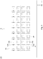
- FIG. 1 is a top view of an antenna array device 100 according to an embodiment of the disclosure, where FIG. 1 is a top view on an x-y plane.
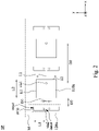
- FIG. 2 shows a top view of a part SP of the antenna array device 100 according to an embodiment of the disclosure, where FIG. 2 is a top view on the x-y plane.
- FIG. 3 is a side view of the part SP of the antenna array device 100 according to an embodiment of the disclosure, where FIG. 3 is a top view on an x-z plane.
- an antenna array device 100 includes a substrate M, a first antenna array P1, a second antenna array P2, and a metal ground plate G.
- the substrate M includes a first surface SF1 and a second surface SF2 corresponding to each other.
- the first antenna array P1 includes multiple antenna elements (e.g., an antenna unit 110a shown in FIG. 1 ), where the multiple antenna elements in the first antenna array P1 is disposed on the first surface SF1, and these antenna elements have a first polarization direction (e.g., a -x direction).
- the second antenna array P2 also includes multiple antenna elements (e.g., an antenna element 110b shown in FIG. 1 ), where the multiple antenna elements in the second antenna array P2 also are disposed on the first surface SF1, and these antenna elements have a second polarization direction (e.g., a x direction) opposite to the first polarization direction.
- multiple antenna elements e.g., an antenna element 110b shown in FIG. 1
- these antenna elements have a second polarization direction (e.g., a x direction) opposite to the first polarization direction.
- first antenna array P1 and the second antenna array P2 in FIGS. 1 to 3 have horizontal polarization directions (i.e., a -x direction and a x direction)
- first antenna array P1 and the second antenna array P2 also have vertical polarization directions (e.g. when the first antenna array P1 and the second antenna array P2 in FIGS. 1 to 3 are turned 90 degrees counterclockwise, the polarization direction of the first antenna array P1 and a polarization direction of the second antenna array P2 are a -y direction and a y direction respectively).
- the metal ground plate G is disposed on the second surface SF2.
- the multiple antenna elements in the first antenna array P1 and the multiple antenna elements in the second antenna array P2 can all be connected to the antenna feed points via respective vias (e.g., a first via via1 in a part SP of the antenna array device 100 in FIG. 2 ).
- the first antenna array P1 further includes multiple isolation unit groups (e.g., an isolation unit group 120a in FIG. 1 ), and the second antenna array P2 also includes multiple isolation unit groups (e.g., an isolation unit group 120b in FIG. 1 ).
- the isolation unit group is disposed between adjacent two of the antenna elements (i.e., one isolation unit group is disposed between all two adjacent antenna elements), where an arrangement direction of the isolation unit group is perpendicular to the first polarization direction and the second polarization direction. For example, when the first polarization direction and the second polarization direction are the -x direction and the x direction respectively, the arrangement direction of the isolation unit group is the y direction.
- the isolation unit group is two isolation units (e.g., an isolation unit strip in the part SP of the antenna array device 100 in FIG. 2 ) which are adjacent, where each of the two isolation units includes an outer end (e.g., an outer end outer on the isolation unit strip in the part SP of the antenna array device 100 of FIG. 2 ) and an inner end opposite to the outer end (e.g., an inner end of the isolation unit strip in the part SP of the antenna array device 100 in FIG. 2 ), and the inner end is connected to the metal ground plate G via a via (e.g., a second via via2 on the isolation unit strip in the part of the antenna array device 100 in FIG. 2 ).
- a via e.g., a second via via2 on the isolation unit strip in the part of the antenna array device 100 in FIG. 2 ).
- the substrate M can be a printed circuit board (PCB) made of an insulating material, and a material of the substrate M can be Teflon (PTFE) or epoxy resin. (FR4) and other materials commonly used to manufacture PCB.
- PCB printed circuit board
- a material of the substrate M can be Teflon (PTFE) or epoxy resin. (FR4) and other materials commonly used to manufacture PCB.
- the first antenna array P1, the second antenna array P2, and the isolation unit group can be directly printed on the substrate M (e.g., multiple patch antennas is printed on the substrate M as the first antenna array P1 and the second antenna array P2, and multiple metal strips is printed on the substrate M as the isolation unit in the isolation unit group).
- the metal ground plate G can be made of metal materials such as copper foil.
- length (e.g., length L1 in the part SP of the antenna array device 100 in FIG. 2 ) of the isolation unit in the isolation unit group can be a quarter wavelength of center frequency of a resonance frequency band of the first antenna array P1 and the second antenna array P2.
- a distance (e.g., a distance D1 in the part SP of the antenna array device 100 in FIG. 2 ) between the isolation units in the isolation unit group can be less than one-twentieth wavelength of the center frequency of the resonance frequency band of the first antenna array P1 and the second antenna array P2.
- a distance (e.g., a distance D2 in the part SP of the antenna array device 100 in FIG. 2 ) between the vias of adjacent two of these above-mentioned antenna elements (i.e., all the antenna elements in the first antenna array P1 and the second antenna array P2) is a half wavelength of the center frequency of the resonance frequency band of the first antenna array P1 and the second antenna array P2.
- the antenna elements in the first antenna array P1 and the second antenna array P2 can both include two edges (e.g., edges E1 and E2 in the part SP of the antenna array device 100 in FIG. 2 ), where length of the two edges (e.g., length L2 in the part SP of the antenna array device 100 in FIG. 2 ) can be equal.
- a distance e.g., a distance D3 in the part SP of the antenna array device 100 in FIG. 2
- a distance D3 in the part SP of the antenna array device 100 in FIG. 2 between the antenna element and the isolation unit group which is adjacent to the antenna element can be one-third the length of the aforementioned edge.
- the isolation unit group can resonate with the above-mentioned antenna elements by the respective vias to isolate signals between the antenna elements.
- a part of the signals generated by the antenna elements can interfere with adjacent antenna elements by positions of the vias of the isolation unit group. Therefore, these vias can be used to resonate with the antenna elements to prevent the part of the signals generated by the antenna elements from interfering with the adjacent antenna elements. In this way, isolation between these antenna elements can be greatly increased, so as to increase a steering angle of each antenna element.
- the above-mentioned antenna array device 100 uses the isolation unit group between two adjacent antenna elements to increase the isolation between the antenna elements, thereby greatly increasing a steering range of each antenna unit.
- second isolation unit group can be disposed between the two adjacent antenna elements. Therefore, an embodiment in which the two isolation unit groups are disposed between the two adjacent antenna elements is proposed below.
- FIG. 4 is a top view of the antenna array device 200 according to another embodiment of the disclosure, where FIG. 4 is the top view on the x-y plane.
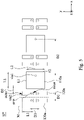
- FIG. 5 is a top view of a part SP' of the antenna array device 200 according to another embodiment of the disclosure, where FIG. 5 is the top view on the x-y plane.
- FIG. 6 is a side view of the part SP' of the antenna array device 200according to another embodiment of the disclosure, where FIG. 6 is the side view on the x-z plane.
- an antenna array device 200 adopts a configuration similar to that of the antenna array device 100 in FIGS.
- a first antenna array P1 and a second antenna array P2 of the antenna array device 200 in addition to one isolation unit group (e.g., isolation unit groups 120a and 120b in FIG. 4 ) disposed between adjacent two of antenna elements, other isolation unit group (e.g., other isolation unit groups 130a and 130b in FIG. 4 ) can be disposed between the adjacent two of the antenna elements.
- the other isolation unit groups are adjacent to the isolation unit group respectively and are disposed between the adjacent two of the antenna elements, where arrangement directions of the other isolation unit groups are parallel to arrangement directions of the isolation unit group respectively.
- a distance (e.g., a distance D1 in a part SP' of the antenna array device 200 in FIG. 5 ) between the other isolation unit group and the adjacent isolation unit group can be less than an one-twentieth wavelength of the center frequency of the resonance frequency band of the first antenna array P1 and the second antenna array P2.
- respective vias of the two isolation unit groups provided between adjacent two of the antenna elements can resonate with the above-mentioned antenna elements to isolate signals between these antenna elements.
- a part of the signals generated by one of the antenna elements can interfere with adjacent antenna elements by positions of the vias of the two isolation unit groups. Therefore, these vias can be used to resonate with the antenna elements to prevent the part of the signals generated by the antenna elements from interfering with the adjacent antenna elements. In this way, isolation (this isolation will be better than a single isolation unit group between adjacent two of the antenna elements) between these antenna elements can be further increased, thereby increasing a steering range of each antenna element.
- isolation unit group have the same structure as the isolation unit group, so it will not be repeated here.
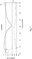
- FIG. 7 is a schematic diagram illustrating a resonance frequency band and isolation (s-parameter and frequency) of the part SP' of the antenna array device 200 according to another embodiment of the disclosure.
- a resonance frequency band op of the part of SP' of the antenna array device 200 is about 27.08 GHz to 29.93 GHz (frequency band with return loss less than -10dB), and its center frequency is about 28 GHz.
- isolation iso of the part SP' of the antenna array device 200 is about -25 dB.
- the isolation iso of the part SP' of the antenna array device 200 fulfills isolation requirements of the fifth-generation new radio (5G NR) standard (i.e., less than -20dB).
- 5G NR fifth-generation new radio
- the above-mentioned antenna array device 200 further increases the isolation between the antenna elements using the two isolation unit groups disposed between the two adjacent antenna elements, thereby greatly increasing a steering angle of each antenna element.
- the antenna array device of the present disclosure greatly increases the isolation of the antenna elements using the above-mentioned arrangement of the isolation units. In this way, when the isolation of each antenna element is greatly increased, the steering angle of the antenna elements can be further increased without causing a coupling effect.
Landscapes
- Variable-Direction Aerials And Aerial Arrays (AREA)
- Waveguide Aerials (AREA)
- Details Of Aerials (AREA)
Abstract
Description
- The present disclosure relates to technology of fifth generation new radio (5G NR). More particularly, the present disclosure relates to an antenna array device.
- In an antenna array of fifth-generation new radio (5G NR) millimeter wave (mmWave), a steering angle is standard of measurement of reachable scanning range of an antenna beam. At present, patch antennas have been widely used in current 5G NR mmWave antenna arrays. However, due to coupling effect between the patch antennas, its scanning angle is often affected. Therefore, how to reduce the coupling effect between the patch antennas to increase the steering angle is a problem that those skilled in the art eager to solve.
- The disclosure provides an antenna array device, which includes a substrate, multiple antenna elements, a metal ground plate and a first isolation unit group. The substrate comprises a first surface and a second surface. The multiple antenna elements are disposed on the first surface, where the multiple antenna elements have a first polarization direction and a second polarization direction opposite to the first polarization direction, and the multiple antenna elements have a first via respectively. The metal ground plate is disposed on the second surface. The first isolation unit group is disposed between adjacent two of the multiple antenna elements, where an arrangement direction of the first isolation unit group is perpendicular to the first polarization direction and the second polarization direction, where the first isolation unit group is two isolation units which are adjacent, each of the two isolation units comprises an outer end and an inner end opposite to the outer end, and the inner end is connected to the metal ground plate via a second via.
- Based on the above, the antenna array device provided by the present disclosure increases isolation between the antenna elements by providing the isolation unit between two of the antenna elements, thereby increasing a steering angle of the antenna elements.
- These and other features, aspects, and advantages of the present disclosure will become better understood with reference to the following description and appended claims.
- It is to be understood that both the foregoing general description and the following detailed description are by examples, and are intended to provide further explanation of the disclosure as claimed.
- The disclosure can be more fully understood by reading the following detailed description of the embodiment, with reference made to the accompanying drawings as follows:
-
FIG. 1 is a top view of an antenna array device according to an embodiment of the disclosure. -
FIG. 2 shows a top view of a part of the antenna array device according to an embodiment of the disclosure. -
FIG. 3 is a side view of a part of the antenna array device according to an embodiment of the disclosure. -
FIG. 4 is a top view of the antenna array device according to another embodiment of the disclosure. -
FIG. 5 is a top view of a part of the antenna array device according to another embodiment of the disclosure. -
FIG. 6 is a side view of the part of the antenna array device according to another embodiment of the disclosure. -
FIG. 7 is a schematic diagram illustrating a resonance frequency band and isolation of the part of the antenna array device according to another embodiment of the disclosure. - Reference will now be made in detail to the present embodiments of the disclosure, examples of which are illustrated in the accompanying drawings. Wherever possible, the same reference numbers are used in the drawings and the description to refer to the same or like parts.
-
FIG. 1 is a top view of anantenna array device 100 according to an embodiment of the disclosure, whereFIG. 1 is a top view on an x-y plane.FIG. 2 shows a top view of a part SP of theantenna array device 100 according to an embodiment of the disclosure, whereFIG. 2 is a top view on the x-y plane.FIG. 3 is a side view of the part SP of theantenna array device 100 according to an embodiment of the disclosure, whereFIG. 3 is a top view on an x-z plane. Referring toFIGS. 1 to 3 at the same time, anantenna array device 100 includes a substrate M, a first antenna array P1, a second antenna array P2, and a metal ground plate G. - Furthermore, the substrate M includes a first surface SF1 and a second surface SF2 corresponding to each other. The first antenna array P1 includes multiple antenna elements (e.g., an
antenna unit 110a shown inFIG. 1 ), where the multiple antenna elements in the first antenna array P1 is disposed on the first surface SF1, and these antenna elements have a first polarization direction (e.g., a -x direction). - In addition, the second antenna array P2 also includes multiple antenna elements (e.g., an
antenna element 110b shown inFIG. 1 ), where the multiple antenna elements in the second antenna array P2 also are disposed on the first surface SF1, and these antenna elements have a second polarization direction (e.g., a x direction) opposite to the first polarization direction. - It is worth noting that, although the first antenna array P1 and the second antenna array P2 in
FIGS. 1 to 3 have horizontal polarization directions (i.e., a -x direction and a x direction), the first antenna array P1 and the second antenna array P2 also have vertical polarization directions (e.g. when the first antenna array P1 and the second antenna array P2 inFIGS. 1 to 3 are turned 90 degrees counterclockwise, the polarization direction of the first antenna array P1 and a polarization direction of the second antenna array P2 are a -y direction and a y direction respectively). - Furthermore, the metal ground plate G is disposed on the second surface SF2. In some embodiments, the multiple antenna elements in the first antenna array P1 and the multiple antenna elements in the second antenna array P2 can all be connected to the antenna feed points via respective vias (e.g., a first via via1 in a part SP of the
antenna array device 100 inFIG. 2 ). - In addition, the first antenna array P1 further includes multiple isolation unit groups (e.g., an
isolation unit group 120a inFIG. 1 ), and the second antenna array P2 also includes multiple isolation unit groups (e.g., anisolation unit group 120b inFIG. 1 ). Further, the isolation unit group is disposed between adjacent two of the antenna elements (i.e., one isolation unit group is disposed between all two adjacent antenna elements), where an arrangement direction of the isolation unit group is perpendicular to the first polarization direction and the second polarization direction. For example, when the first polarization direction and the second polarization direction are the -x direction and the x direction respectively, the arrangement direction of the isolation unit group is the y direction. - In this embodiment, the isolation unit group is two isolation units (e.g., an isolation unit strip in the part SP of the
antenna array device 100 inFIG. 2 ) which are adjacent, where each of the two isolation units includes an outer end (e.g., an outer end outer on the isolation unit strip in the part SP of theantenna array device 100 ofFIG. 2 ) and an inner end opposite to the outer end (e.g., an inner end of the isolation unit strip in the part SP of theantenna array device 100 inFIG. 2 ), and the inner end is connected to the metal ground plate G via a via (e.g., a second via via2 on the isolation unit strip in the part of theantenna array device 100 inFIG. 2 ). - In some embodiments, the substrate M can be a printed circuit board (PCB) made of an insulating material, and a material of the substrate M can be Teflon (PTFE) or epoxy resin. (FR4) and other materials commonly used to manufacture PCB. In this way, the first antenna array P1, the second antenna array P2, and the isolation unit group can be directly printed on the substrate M (e.g., multiple patch antennas is printed on the substrate M as the first antenna array P1 and the second antenna array P2, and multiple metal strips is printed on the substrate M as the isolation unit in the isolation unit group). In addition, the metal ground plate G can be made of metal materials such as copper foil.
- In some embodiments, length (e.g., length L1 in the part SP of the
antenna array device 100 inFIG. 2 ) of the isolation unit in the isolation unit group can be a quarter wavelength of center frequency of a resonance frequency band of the first antenna array P1 and the second antenna array P2. - In some embodiments, a distance (e.g., a distance D1 in the part SP of the
antenna array device 100 inFIG. 2 ) between the isolation units in the isolation unit group can be less than one-twentieth wavelength of the center frequency of the resonance frequency band of the first antenna array P1 and the second antenna array P2. - In some embodiments, a distance (e.g., a distance D2 in the part SP of the
antenna array device 100 inFIG. 2 ) between the vias of adjacent two of these above-mentioned antenna elements (i.e., all the antenna elements in the first antenna array P1 and the second antenna array P2) is a half wavelength of the center frequency of the resonance frequency band of the first antenna array P1 and the second antenna array P2. - In some embodiments, the antenna elements in the first antenna array P1 and the second antenna array P2 can both include two edges (e.g., edges E1 and E2 in the part SP of the
antenna array device 100 inFIG. 2 ), where length of the two edges (e.g., length L2 in the part SP of theantenna array device 100 inFIG. 2 ) can be equal. In a further embodiment, a distance (e.g., a distance D3 in the part SP of theantenna array device 100 inFIG. 2 ) between the antenna element and the isolation unit group which is adjacent to the antenna element can be one-third the length of the aforementioned edge. - In some embodiments, the isolation unit group can resonate with the above-mentioned antenna elements by the respective vias to isolate signals between the antenna elements. In other words, a part of the signals generated by the antenna elements can interfere with adjacent antenna elements by positions of the vias of the isolation unit group. Therefore, these vias can be used to resonate with the antenna elements to prevent the part of the signals generated by the antenna elements from interfering with the adjacent antenna elements. In this way, isolation between these antenna elements can be greatly increased, so as to increase a steering angle of each antenna element.
- Based on the above, the above-mentioned
antenna array device 100 uses the isolation unit group between two adjacent antenna elements to increase the isolation between the antenna elements, thereby greatly increasing a steering range of each antenna unit. - It is worth noting that, in addition to one isolation unit group disposed between the two adjacent antenna elements, second isolation unit group can be disposed between the two adjacent antenna elements. Therefore, an embodiment in which the two isolation unit groups are disposed between the two adjacent antenna elements is proposed below.
-
FIG. 4 is a top view of theantenna array device 200 according to another embodiment of the disclosure, whereFIG. 4 is the top view on the x-y plane.FIG. 5 is a top view of a part SP' of theantenna array device 200 according to another embodiment of the disclosure, whereFIG. 5 is the top view on the x-y plane.FIG. 6 is a side view of the part SP' of the antenna array device 200according to another embodiment of the disclosure, whereFIG. 6 is the side view on the x-z plane. Referring toFIGS. 4 to 6 at the same time, anantenna array device 200 adopts a configuration similar to that of theantenna array device 100 inFIGS. 1 to 3 , where differences between the two are only in a number of isolation unit groups provided between two adjacent antenna elements (i.e., theantenna array device 200 adopts arrangement of two isolation unit groups, and theantenna array device 100 adopts arrangement of the one isolation unit group). Therefore, only the differences are described here, and the rest of similarities will not be repeated. - In detail, in a first antenna array P1 and a second antenna array P2 of the
antenna array device 200, in addition to one isolation unit group (e.g.,isolation unit groups FIG. 4 ) disposed between adjacent two of antenna elements, other isolation unit group (e.g., otherisolation unit groups FIG. 4 ) can be disposed between the adjacent two of the antenna elements. In other words, the other isolation unit groups are adjacent to the isolation unit group respectively and are disposed between the adjacent two of the antenna elements, where arrangement directions of the other isolation unit groups are parallel to arrangement directions of the isolation unit group respectively. - In some embodiments, a distance (e.g., a distance D1 in a part SP' of the
antenna array device 200 inFIG. 5 ) between the other isolation unit group and the adjacent isolation unit group can be less than an one-twentieth wavelength of the center frequency of the resonance frequency band of the first antenna array P1 and the second antenna array P2. - In some embodiments, respective vias of the two isolation unit groups provided between adjacent two of the antenna elements can resonate with the above-mentioned antenna elements to isolate signals between these antenna elements. In other words, a part of the signals generated by one of the antenna elements can interfere with adjacent antenna elements by positions of the vias of the two isolation unit groups. Therefore, these vias can be used to resonate with the antenna elements to prevent the part of the signals generated by the antenna elements from interfering with the adjacent antenna elements. In this way, isolation (this isolation will be better than a single isolation unit group between adjacent two of the antenna elements) between these antenna elements can be further increased, thereby increasing a steering range of each antenna element.
- It is worth noting that the other isolation unit group have the same structure as the isolation unit group, so it will not be repeated here.
-
FIG. 7 is a schematic diagram illustrating a resonance frequency band and isolation (s-parameter and frequency) of the part SP' of theantenna array device 200 according to another embodiment of the disclosure. Referring toFIGS. 4 to 7 at the same time, a resonance frequency band op of the part of SP' of theantenna array device 200 is about 27.08 GHz to 29.93 GHz (frequency band with return loss less than -10dB), and its center frequency is about 28 GHz. In this way, isolation iso of the part SP' of theantenna array device 200 is about -25 dB. In other words, the isolation iso of the part SP' of theantenna array device 200 fulfills isolation requirements of the fifth-generation new radio (5G NR) standard (i.e., less than -20dB). - Based on the above, the above-mentioned
antenna array device 200 further increases the isolation between the antenna elements using the two isolation unit groups disposed between the two adjacent antenna elements, thereby greatly increasing a steering angle of each antenna element. - In summary, the antenna array device of the present disclosure greatly increases the isolation of the antenna elements using the above-mentioned arrangement of the isolation units. In this way, when the isolation of each antenna element is greatly increased, the steering angle of the antenna elements can be further increased without causing a coupling effect.
Claims (10)
- An antenna array device (100), comprising:a substrate (M), comprising a first surface (SF1) and a second surface (SF2);a plurality of antenna elements (110a and 110b), disposed on the first surface (SF1), wherein the plurality of antenna elements (110a and 110b) have a first polarization direction and a second polarization direction opposite to the first polarization direction, and the plurality of antenna elements (110a and 110b) have a first via (via1) respectively;a metal ground plate (G), disposed on the second surface (SF2); anda first isolation unit group (120a and 120b), disposed between adjacent two of the plurality of antenna elements (110a and 110b), wherein an arrangement direction of the first isolation unit group (120a and 120b) is perpendicular to the first polarization direction and the second polarization direction, wherein the first isolation unit group (120a and 120b) is two isolation units (strip) which are adjacent, each of the two isolation units (strip) comprises an outer end and an inner end opposite to the outer end, and the inner end is connected to the metal ground plate (G) via a second via (via2).
- The antenna array device (100) of claim 1, further comprising a second isolation unit group (130a and 130b), the second isolation unit group (130a and 130b) is adjacent to the first isolation unit group (120a and 120b) respectively, and is disposed between the adjacent two of the plurality of antenna elements (110a and 110b).
- The antenna array device (100) of claim 2, wherein an arrangement direction of the second isolation unit group (130a and 130b) is parallel to the arrangement direction of the first isolation unit group (120a and 120b), wherein the plurality of antenna elements (110a and 110b) are connected to antenna feed points via the respective first via (via1).
- The antenna array device (100) of claim 3, wherein a distance between the first vias (via1) of the adjacent two of the plurality of antenna elements (110a and 110b) is a half wavelength of center frequency of a resonance frequency band of the plurality of antenna elements (110a and 110b).
- The antenna array device (100) of claim 2, wherein the first isolation unit group (120a and 120b) and the second isolation unit group (130a and 130b) are arranged between each two antenna elements (110a and 110b) of the plurality of antenna elements (110a and 110b) respectively.
- The antenna array device (100) of claim 1, further comprising:a third isolation unit group; anda fourth isolation unit group, wherein the third isolation unit group and the fourth isolation unit group are arranged between each two antenna elements (110a and 110b) of the plurality of antenna elements (110a and 110b) respectively.
- The antenna array device (100) of claim 1, wherein the two isolation units (strip) are composed of two metal strips, and length of the metal strips is a quarter wavelength of center frequency of a resonance frequency band of the plurality of antenna elements (110a and 110b).
- The antenna array device (100) of claim 1, wherein a distance between the two isolation units (strip) is less than one-twentieth wavelength of center frequency of a resonance frequency band of the plurality of antenna elements (110a and 110b).
- The antenna array device (100) of claim 1, wherein each of the plurality of antenna elements (110a and 110b) comprises an edge (E1), wherein a plurality of separation distances exists between the plurality of antenna elements (110a and 110b) and the first isolation unit group (120a and 120b), and length of the separation distances is one-third of length of the above-mentioned edge (E1).
- The antenna array device (100) of claim 1, wherein the first polarization direction and the second polarization direction both are horizontal polarization directions, or both are vertical polarization directions.
Applications Claiming Priority (1)
| Application Number | Priority Date | Filing Date | Title |
|---|---|---|---|
| CN202110520119.1A CN115347380B (en) | 2021-05-13 | 2021-05-13 | Antenna array device |
Publications (3)
| Publication Number | Publication Date |
|---|---|
| EP4089838A1 true EP4089838A1 (en) | 2022-11-16 |
| EP4089838C0 EP4089838C0 (en) | 2025-02-19 |
| EP4089838B1 EP4089838B1 (en) | 2025-02-19 |
Family
ID=78483212
Family Applications (1)
| Application Number | Title | Priority Date | Filing Date |
|---|---|---|---|
| EP21205775.6A Active EP4089838B1 (en) | 2021-05-13 | 2021-11-01 | Antenna array device |
Country Status (5)
| Country | Link |
|---|---|
| US (1) | US12191574B2 (en) |
| EP (1) | EP4089838B1 (en) |
| JP (1) | JP7168146B1 (en) |
| CN (1) | CN115347380B (en) |
| ES (1) | ES3026757T3 (en) |
Families Citing this family (5)
| Publication number | Priority date | Publication date | Assignee | Title |
|---|---|---|---|---|
| CN115732931A (en) * | 2021-09-01 | 2023-03-03 | 台达电子工业股份有限公司 | Antenna array device |
| JP2024047278A (en) * | 2022-09-26 | 2024-04-05 | 株式会社東芝 | Planar Antenna Device |
| US12489199B2 (en) * | 2022-12-21 | 2025-12-02 | Outdoor Wireless Networks LLC | Base station antennas having partially reflective surface isolation walls |
| CN117175207B (en) * | 2023-09-27 | 2024-06-25 | 普罗斯通信技术(苏州)有限公司 | Antenna |
| CN120073312A (en) * | 2023-11-29 | 2025-05-30 | 深圳富泰宏精密工业有限公司 | Array antenna module and wireless communication device |
Citations (3)
| Publication number | Priority date | Publication date | Assignee | Title |
|---|---|---|---|---|
| US20120190296A1 (en) * | 2010-05-28 | 2012-07-26 | The Regents Of The University Of Michigan | Miniaturized radio repeater |
| CN111710970A (en) * | 2020-06-08 | 2020-09-25 | Oppo广东移动通信有限公司 | mmWave antenna modules and electronic equipment |
| US20210005955A1 (en) * | 2019-01-25 | 2021-01-07 | Murata Manufacturing Co., Ltd. | Antenna module and communication apparatus equipped with the same |
Family Cites Families (27)
| Publication number | Priority date | Publication date | Assignee | Title |
|---|---|---|---|---|
| SE513138C2 (en) * | 1998-11-20 | 2000-07-10 | Ericsson Telefon Ab L M | Method and arrangement for increasing the isolation between antennas |
| US7916089B2 (en) * | 2008-01-04 | 2011-03-29 | Apple Inc. | Antenna isolation for portable electronic devices |
| CN102204013A (en) | 2008-09-30 | 2011-09-28 | 纽帕尔斯有限公司 | Multilayer antenna |
| KR101060457B1 (en) * | 2009-05-19 | 2011-08-29 | 경기대학교 산학협력단 | Soft surface structure isolated from ground plane and antenna using it |
| JP5076019B1 (en) * | 2011-10-19 | 2012-11-21 | 株式会社東芝 | ANTENNA DEVICE AND ELECTRONIC DEVICE HAVING THE ANTENNA DEVICE |
| CN103703620B (en) * | 2013-08-26 | 2016-12-14 | 华为技术有限公司 | Wideband dual-polarization array antenna and base station |
| CN105322291B (en) | 2014-07-24 | 2019-07-23 | 深圳光启创新技术有限公司 | Micro-strip array antenna |
| TWI583052B (en) * | 2014-10-15 | 2017-05-11 | 宏碁股份有限公司 | Mobile device |
| US10122074B2 (en) * | 2014-11-19 | 2018-11-06 | Panasonic Intellectual Property Management Co., Ltd. | Antenna device using EBG structure, wireless communication device, and radar device |
| US9866069B2 (en) * | 2014-12-29 | 2018-01-09 | Ricoh Co., Ltd. | Manually beam steered phased array |
| GB2548115B (en) * | 2016-03-08 | 2019-04-24 | Cambium Networks Ltd | Antenna array assembly with a T-shaped isolator bar |
| JP2018164149A (en) * | 2017-03-24 | 2018-10-18 | パナソニック株式会社 | Antenna device |
| WO2018235593A1 (en) * | 2017-06-23 | 2018-12-27 | 株式会社ソシオネクスト | Antenna device |
| CN111527646B (en) * | 2017-12-28 | 2021-08-03 | 株式会社村田制作所 | Antenna Arrays and Antenna Modules |
| CN108448239B (en) * | 2018-02-28 | 2019-11-15 | 维沃移动通信有限公司 | A millimeter wave antenna array and mobile terminal |
| KR102017159B1 (en) * | 2018-03-12 | 2019-09-02 | 삼성전자주식회사 | Antenna module |
| US11139588B2 (en) * | 2018-04-11 | 2021-10-05 | Apple Inc. | Electronic device antenna arrays mounted against a dielectric layer |
| JP6973663B2 (en) * | 2018-11-15 | 2021-12-01 | 株式会社村田製作所 | Antenna module and communication device |
| CN114175400B (en) * | 2019-05-27 | 2026-03-24 | 株式会社村田制作所 | Antenna module and communication device equipped with the antenna module |
| JP6798657B1 (en) * | 2019-06-28 | 2020-12-09 | 株式会社村田製作所 | Antenna module and communication device equipped with it |
| KR102676501B1 (en) * | 2019-07-03 | 2024-06-18 | 삼성전기주식회사 | Antenna apparatus |
| US11316283B2 (en) * | 2019-07-24 | 2022-04-26 | Delta Electronics, Inc. | Dual polarized antenna |
| CN112290234A (en) * | 2019-07-24 | 2021-01-29 | 台达电子工业股份有限公司 | communication device |
| EP3819985B1 (en) * | 2019-11-08 | 2024-04-24 | Carrier Corporation | Microstrip patch antenna with increased bandwidth |
| US20210239788A1 (en) * | 2020-02-05 | 2021-08-05 | Alps Alpine Co., Ltd. | Radar with virtual planar array (vpa) antenna |
| KR20220070991A (en) * | 2020-11-23 | 2022-05-31 | 삼성전기주식회사 | Antenna apparatus |
| CN112448172B (en) | 2021-02-01 | 2021-04-20 | 成都天锐星通科技有限公司 | Planar phased array antenna |
-
2021
- 2021-05-13 CN CN202110520119.1A patent/CN115347380B/en active Active
- 2021-09-28 JP JP2021158497A patent/JP7168146B1/en active Active
- 2021-10-05 US US17/450,069 patent/US12191574B2/en active Active
- 2021-11-01 EP EP21205775.6A patent/EP4089838B1/en active Active
- 2021-11-01 ES ES21205775T patent/ES3026757T3/en active Active
Patent Citations (3)
| Publication number | Priority date | Publication date | Assignee | Title |
|---|---|---|---|---|
| US20120190296A1 (en) * | 2010-05-28 | 2012-07-26 | The Regents Of The University Of Michigan | Miniaturized radio repeater |
| US20210005955A1 (en) * | 2019-01-25 | 2021-01-07 | Murata Manufacturing Co., Ltd. | Antenna module and communication apparatus equipped with the same |
| CN111710970A (en) * | 2020-06-08 | 2020-09-25 | Oppo广东移动通信有限公司 | mmWave antenna modules and electronic equipment |
Also Published As
| Publication number | Publication date |
|---|---|
| CN115347380A (en) | 2022-11-15 |
| JP7168146B1 (en) | 2022-11-09 |
| JP2022176032A (en) | 2022-11-25 |
| US12191574B2 (en) | 2025-01-07 |
| ES3026757T3 (en) | 2025-06-12 |
| EP4089838C0 (en) | 2025-02-19 |
| EP4089838B1 (en) | 2025-02-19 |
| US20220368034A1 (en) | 2022-11-17 |
| CN115347380B (en) | 2025-09-12 |
Similar Documents
| Publication | Publication Date | Title |
|---|---|---|
| EP4089838B1 (en) | Antenna array device | |
| US10957971B2 (en) | Feed to waveguide transition structures and related sensor assemblies | |
| US6795021B2 (en) | Tunable multi-band antenna array | |
| US5165109A (en) | Microwave communication antenna | |
| US10424847B2 (en) | Wideband dual-polarized current loop antenna element | |
| US20190089069A1 (en) | Broadband phased array antenna system with hybrid radiating elements | |
| US11271319B2 (en) | Antennas for reception of satellite signals | |
| US12278435B2 (en) | Miniature antenna with omnidirectional radiation field | |
| CN111525255A (en) | Low-profile broadband wide-angle tightly-coupled antenna unit and array | |
| US20170317422A1 (en) | Low Profile Wideband Planar Antenna Element With Integrated Baluns | |
| US12394900B2 (en) | Bandwidth extended balanced tightly coupled dipole array additively manufactured modular aperture | |
| EP4075601B1 (en) | Antenna structure and wireless communication device | |
| CN212162078U (en) | A Low Profile Wide Bandwidth Angle Tightly Coupled Antenna Unit and Array | |
| US11721908B2 (en) | Antenna structure with wide beamwidth | |
| KR20230052577A (en) | Chip patch antenna and chip patch antenna module | |
| US12155120B2 (en) | Antenna array device | |
| TWI767699B (en) | Antenna array device | |
| TWI763439B (en) | Antenna structure and wireless communication device | |
| US20250183554A1 (en) | Antenna structure, antenna array and antenna module | |
| US11677137B2 (en) | Electronic device | |
| US11223130B2 (en) | Antenna structure | |
| Livadaru et al. | Realization of Low-Cost Wide Scanning Arrays |
Legal Events
| Date | Code | Title | Description |
|---|---|---|---|
| PUAI | Public reference made under article 153(3) epc to a published international application that has entered the european phase |
Free format text: ORIGINAL CODE: 0009012 |
|
| STAA | Information on the status of an ep patent application or granted ep patent |
Free format text: STATUS: THE APPLICATION HAS BEEN PUBLISHED |
|
| AK | Designated contracting states |
Kind code of ref document: A1 Designated state(s): AL AT BE BG CH CY CZ DE DK EE ES FI FR GB GR HR HU IE IS IT LI LT LU LV MC MK MT NL NO PL PT RO RS SE SI SK SM TR |
|
| STAA | Information on the status of an ep patent application or granted ep patent |
Free format text: STATUS: REQUEST FOR EXAMINATION WAS MADE |
|
| 17P | Request for examination filed |
Effective date: 20221219 |
|
| RBV | Designated contracting states (corrected) |
Designated state(s): AL AT BE BG CH CY CZ DE DK EE ES FI FR GB GR HR HU IE IS IT LI LT LU LV MC MK MT NL NO PL PT RO RS SE SI SK SM TR |
|
| STAA | Information on the status of an ep patent application or granted ep patent |
Free format text: STATUS: EXAMINATION IS IN PROGRESS |
|
| 17Q | First examination report despatched |
Effective date: 20230808 |
|
| GRAP | Despatch of communication of intention to grant a patent |
Free format text: ORIGINAL CODE: EPIDOSNIGR1 |
|
| STAA | Information on the status of an ep patent application or granted ep patent |
Free format text: STATUS: GRANT OF PATENT IS INTENDED |
|
| INTG | Intention to grant announced |
Effective date: 20241009 |
|
| GRAS | Grant fee paid |
Free format text: ORIGINAL CODE: EPIDOSNIGR3 |
|
| GRAA | (expected) grant |
Free format text: ORIGINAL CODE: 0009210 |
|
| STAA | Information on the status of an ep patent application or granted ep patent |
Free format text: STATUS: THE PATENT HAS BEEN GRANTED |
|
| AK | Designated contracting states |
Kind code of ref document: B1 Designated state(s): AL AT BE BG CH CY CZ DE DK EE ES FI FR GB GR HR HU IE IS IT LI LT LU LV MC MK MT NL NO PL PT RO RS SE SI SK SM TR |
|
| REG | Reference to a national code |
Ref country code: GB Ref legal event code: FG4D |
|
| REG | Reference to a national code |
Ref country code: CH Ref legal event code: EP |
|
| REG | Reference to a national code |
Ref country code: DE Ref legal event code: R096 Ref document number: 602021026300 Country of ref document: DE |
|
| REG | Reference to a national code |
Ref country code: IE Ref legal event code: FG4D |
|
| U01 | Request for unitary effect filed |
Effective date: 20250307 |
|
| U07 | Unitary effect registered |
Designated state(s): AT BE BG DE DK EE FI FR IT LT LU LV MT NL PT RO SE SI Effective date: 20250314 |
|
| REG | Reference to a national code |
Ref country code: ES Ref legal event code: FG2A Ref document number: 3026757 Country of ref document: ES Kind code of ref document: T3 Effective date: 20250612 |
|
| PG25 | Lapsed in a contracting state [announced via postgrant information from national office to epo] |
Ref country code: RS Free format text: LAPSE BECAUSE OF FAILURE TO SUBMIT A TRANSLATION OF THE DESCRIPTION OR TO PAY THE FEE WITHIN THE PRESCRIBED TIME-LIMIT Effective date: 20250519 |
|
| PG25 | Lapsed in a contracting state [announced via postgrant information from national office to epo] |
Ref country code: PL Free format text: LAPSE BECAUSE OF FAILURE TO SUBMIT A TRANSLATION OF THE DESCRIPTION OR TO PAY THE FEE WITHIN THE PRESCRIBED TIME-LIMIT Effective date: 20250219 |
|
| PG25 | Lapsed in a contracting state [announced via postgrant information from national office to epo] |
Ref country code: NO Free format text: LAPSE BECAUSE OF FAILURE TO SUBMIT A TRANSLATION OF THE DESCRIPTION OR TO PAY THE FEE WITHIN THE PRESCRIBED TIME-LIMIT Effective date: 20250519 Ref country code: IS Free format text: LAPSE BECAUSE OF FAILURE TO SUBMIT A TRANSLATION OF THE DESCRIPTION OR TO PAY THE FEE WITHIN THE PRESCRIBED TIME-LIMIT Effective date: 20250619 |
|
| PG25 | Lapsed in a contracting state [announced via postgrant information from national office to epo] |
Ref country code: HR Free format text: LAPSE BECAUSE OF FAILURE TO SUBMIT A TRANSLATION OF THE DESCRIPTION OR TO PAY THE FEE WITHIN THE PRESCRIBED TIME-LIMIT Effective date: 20250219 |
|
| PG25 | Lapsed in a contracting state [announced via postgrant information from national office to epo] |
Ref country code: GR Free format text: LAPSE BECAUSE OF FAILURE TO SUBMIT A TRANSLATION OF THE DESCRIPTION OR TO PAY THE FEE WITHIN THE PRESCRIBED TIME-LIMIT Effective date: 20250520 |
|
| PG25 | Lapsed in a contracting state [announced via postgrant information from national office to epo] |
Ref country code: SM Free format text: LAPSE BECAUSE OF FAILURE TO SUBMIT A TRANSLATION OF THE DESCRIPTION OR TO PAY THE FEE WITHIN THE PRESCRIBED TIME-LIMIT Effective date: 20250219 |
|
| PGFP | Annual fee paid to national office [announced via postgrant information from national office to epo] |
Ref country code: GB Payment date: 20250911 Year of fee payment: 5 |
|
| PG25 | Lapsed in a contracting state [announced via postgrant information from national office to epo] |
Ref country code: CZ Free format text: LAPSE BECAUSE OF FAILURE TO SUBMIT A TRANSLATION OF THE DESCRIPTION OR TO PAY THE FEE WITHIN THE PRESCRIBED TIME-LIMIT Effective date: 20250219 |
|
| PG25 | Lapsed in a contracting state [announced via postgrant information from national office to epo] |
Ref country code: SK Free format text: LAPSE BECAUSE OF FAILURE TO SUBMIT A TRANSLATION OF THE DESCRIPTION OR TO PAY THE FEE WITHIN THE PRESCRIBED TIME-LIMIT Effective date: 20250219 |
|
| U20 | Renewal fee for the european patent with unitary effect paid |
Year of fee payment: 5 Effective date: 20251008 |
|
| PLBE | No opposition filed within time limit |
Free format text: ORIGINAL CODE: 0009261 |
|
| STAA | Information on the status of an ep patent application or granted ep patent |
Free format text: STATUS: NO OPPOSITION FILED WITHIN TIME LIMIT |
|
| 26N | No opposition filed |
Effective date: 20251120 |
|
| PGFP | Annual fee paid to national office [announced via postgrant information from national office to epo] |
Ref country code: ES Payment date: 20251212 Year of fee payment: 5 |