EP4089576B1 - Fingerabdruckerkennungsvorrichtung und elektronische vorrichtung - Google Patents
Fingerabdruckerkennungsvorrichtung und elektronische vorrichtung Download PDFInfo
- Publication number
- EP4089576B1 EP4089576B1 EP21912303.1A EP21912303A EP4089576B1 EP 4089576 B1 EP4089576 B1 EP 4089576B1 EP 21912303 A EP21912303 A EP 21912303A EP 4089576 B1 EP4089576 B1 EP 4089576B1
- Authority
- EP
- European Patent Office
- Prior art keywords
- light shielding
- light
- fingerprint identification
- shielding layer
- layer
- Prior art date
- Legal status (The legal status is an assumption and is not a legal conclusion. Google has not performed a legal analysis and makes no representation as to the accuracy of the status listed.)
- Active
Links
Images




Classifications
-
- G—PHYSICS
- G02—OPTICS
- G02B—OPTICAL ELEMENTS, SYSTEMS OR APPARATUS
- G02B3/00—Simple or compound lenses
- G02B3/0006—Arrays
- G02B3/0037—Arrays characterized by the distribution or form of lenses
- G02B3/0056—Arrays characterized by the distribution or form of lenses arranged along two different directions in a plane, e.g. honeycomb arrangement of lenses
-
- G—PHYSICS
- G02—OPTICS
- G02B—OPTICAL ELEMENTS, SYSTEMS OR APPARATUS
- G02B27/00—Optical systems or apparatus not provided for by any of the groups G02B1/00 - G02B26/00, G02B30/00
- G02B27/30—Collimators
-
- G—PHYSICS
- G02—OPTICS
- G02B—OPTICAL ELEMENTS, SYSTEMS OR APPARATUS
- G02B3/00—Simple or compound lenses
- G02B3/0006—Arrays
-
- G—PHYSICS
- G02—OPTICS
- G02B—OPTICAL ELEMENTS, SYSTEMS OR APPARATUS
- G02B5/00—Optical elements other than lenses
- G02B5/003—Light absorbing elements
-
- G—PHYSICS
- G06—COMPUTING OR CALCULATING; COUNTING
- G06V—IMAGE OR VIDEO RECOGNITION OR UNDERSTANDING
- G06V40/00—Recognition of biometric, human-related or animal-related patterns in image or video data
- G06V40/10—Human or animal bodies, e.g. vehicle occupants or pedestrians; Body parts, e.g. hands
- G06V40/12—Fingerprints or palmprints
- G06V40/13—Sensors therefor
- G06V40/1318—Sensors therefor using electro-optical elements or layers, e.g. electroluminescent sensing
-
- G—PHYSICS
- G02—OPTICS
- G02B—OPTICAL ELEMENTS, SYSTEMS OR APPARATUS
- G02B30/00—Optical systems or apparatus for producing three-dimensional [3D] effects, e.g. stereoscopic images
- G02B30/20—Optical systems or apparatus for producing three-dimensional [3D] effects, e.g. stereoscopic images by providing first and second parallax images to an observer's left and right eyes
- G02B30/26—Optical systems or apparatus for producing three-dimensional [3D] effects, e.g. stereoscopic images by providing first and second parallax images to an observer's left and right eyes of the autostereoscopic type
- G02B30/30—Optical systems or apparatus for producing three-dimensional [3D] effects, e.g. stereoscopic images by providing first and second parallax images to an observer's left and right eyes of the autostereoscopic type involving parallax barriers
- G02B30/32—Optical systems or apparatus for producing three-dimensional [3D] effects, e.g. stereoscopic images by providing first and second parallax images to an observer's left and right eyes of the autostereoscopic type involving parallax barriers characterised by the geometry of the parallax barriers, e.g. staggered barriers, slanted parallax arrays or parallax arrays of varying shape or size
Definitions
- Embodiments of the present application relate to the field of fingerprint identification, and more particularly, to a fingerprint identification apparatus and an electronic device.
- D1 ( CN111598068A ) discloses a fingerprint recognition device and electronic equipment, and aims to improve the fingerprint imaging quality while realizing lightening and thinning of the fingerprint recognition device.
- the fingerprint recognition device is suitable for the lower part of a display screen and comprises a plurality of fingerprint recognition units distributed in an array, and each fingerprint recognition unit comprises a micro lens; at least one light blocking layer, each light blocking layer is provided with a small light through hole, N small light through holes are formed in the bottom light blocking layer, and the maximum aperture D1 of each small light through hole and the maximum aperture CA of the micro lens meet the condition that D1/CA is larger than or equal to 0.02 and smaller than or equal to 0.4, so that N light guide channels in different directions are formed; the N pixel units are arranged below the at least one light blocking layer and are arranged at the bottoms of the N light guide channels in a one-to-one correspondence manner; after fingerprint optical signals returned from a finger above the display screen are converged through the micro lens, N target fingerprint optical signals in different directions are transmitted to N pixel units through N light guide channels respectively and used for fingerprint recognition.
- D2 discloses a fingerprint detection device and an electronic device.
- the fingerprint detection device is arranged in an array or staggered with multiple fingerprint detection units.
- Each fingerprint detection unit includes: at least one micro lens.
- the oblique optical signals in the 2M directions reflected from fingers above a display screen are condensed by the at least one microlens, and then transmitted to the plurality of optical fibersthrough the openings provided in the at least one light blocking layer.
- the oblique light signal is used to detect fingerprint information of the fingers.
- M is a positive integer.
- D3 discloses a fingerprint detecting device and electronic equipment.
- the fingerprint detecting device is suitable for locating below a display screen for realizing under-screen optical fingerprint detection.
- Under-screen fingerprint identification technology is the most widely used under-screen optical fingerprint identification technology. Due to the particularity of an under-screen optical fingerprint device, light with a fingerprint signal is required to pass through a screen to be transmitted to a fingerprint sensor thereunder, so that a fingerprint signal is obtained.
- an embodiment of the present application may be applied to an optical fingerprint system, including but not limited to an optical fingerprint identification system and a product based on optical fingerprint imaging.
- the embodiment of the present application is described only by an example of an optical fingerprint system, which should not constitute any limitation to the embodiment of the present application, and the embodiment of the present application is also applicable to another system using optical imaging technology or the like.
- the optical fingerprint system provided in the embodiment of the present application may be applied to portable or mobile computing devices such as a smart phone, a tablet computer and a game device, and other electronic devices such as an electronic database, an automobile and an automated teller machine (ATM), which is not limited in the embodiment of the present application; and the embodiment of the present application may be applied to other mobile terminals having display screens or other electronic devices.
- a fingerprint identification apparatus may be specifically an optical fingerprint apparatus, which may be disposed in a partial region or an entire region under a display screen, thereby forming an under-display optical fingerprint system.
- an under-screen fingerprint identification apparatus includes an optical component, and the optical component may be disposed above an optical fingerprint sensor, which may include a filter layer, a light path directing structure, and other optical elements.
- a small hole can direct a light signal reflected by a finger to a sensor chip under a display screen for fingerprint identification.
- a size of the small hole cannot be further reduced, which limits improvement of its resolution.
- the small hole only allows a light signal in a vertical direction to enter, which results in that imaging signals are limited and enough light signals cannot be provided to a capturing region of the sensor chip.
- the other method is to perform imaging by using an optical lens, which uses a spherical or aspherical lens for converging light so as to improve imaging resolution.
- the lens since the lens has the function of converging light, the lens imaging can direct more light signals to reach a sensor chip compared to the method of small hole imaging.
- the fingerprint identification apparatus may include a micro lens array and a light shielding layer, the micro lens array may be disposed above the light shielding layer, and the light shielding layer is provided with an array of small holes.
- the micro lens array is configured to converge a light signal reflected by a finger to the array of small holes, and the array of small holes may direct a received light signal to a fingerprint sensor chip under the light shielding layer.
- the fingerprint sensor chip may perform fingerprint identification according to the received light signal.
- the micro lens has the function of converging light, so as to be able to improve resolution of an image generated by the fingerprint sensor chip.
- the array of small holes has the function of screening light signals. For example, the array of small holes does not allow an interference light signal with a large angle to pass through, but only allows a light signal within a desired specific angle range to pass through, so as to improve a fingerprint identification effect.
- a sensing array in a fingerprint identification apparatus may also be referred to as a pixel array, and an optical sensing unit or a sensing unit in a sensing array may also be referred to as a pixel unit.
- an optical fingerprint sensor in the fingerprint identification apparatus may also be referred to as a fingerprint sensor or a fingerprint sensor chip.
- the fingerprint identification apparatus in the embodiment of the present application may also be referred to as an optical fingerprint apparatus, an optical fingerprint identification module, a fingerprint identification module, a fingerprint module, a fingerprint capturing apparatus, or the like, and the foregoing terms may be replaced with each other.
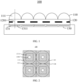
- FIGS. 1 and 2 are a schematic sectional view and a schematic top view of a typical fingerprint identification apparatus.
- a fingerprint identification apparatus 100 includes a micro lens array 110, at least one light shielding layer 120, and a pixel array 130.
- the micro lens array 110 is located directly above the pixel array 130 and the at least one light shielding layer 120, and one micro lens 111 corresponds to one pixel unit 131, that is, each micro lens 111 in the micro lens array 110 focuses received light to a pixel unit 131 corresponding to the same micro-lens 111 through a hole 1201 of the at least one light shielding layer 120.
- a light signal received by each micro lens 111 is mainly a fingerprint light signal incident perpendicular to the micro lens array 110 after being reflected or scattered by a finger above a display screen.
- pixel units 131 in the pixel array 130 are periodically arranged, and a photosensitive region 1311 of each pixel unit 131 in the pixel array 130 is disposed in a center position of the same pixel unit to improve a duty cycle of the photosensitive region.
- a plurality of micro lenses 111 in the micro lens array 110 and a plurality of pixel units 131 in the pixel array 130 are in one-to-one correspondence, and photosensitive regions 1311 of the plurality of pixel units 131 in the pixel array 130 are periodically arranged and uniformly distributed.
- the photosensitive regions of the pixel array 130 are affected by the size of the micro-lens array 110, and a thickness of the fingerprint identification apparatus 100 is relatively large, which further increases processing difficulty, period and costs of a light path of the fingerprint identification apparatus 100.
- the fingerprint identification apparatus 100 since a plurality of micro lenses are close to each other, light may be incident on a chip surface from other micro lenses, thus affecting an imaging effect. And since the micro lenses and the pixel units are in one-to-one correspondence, a theoretical maximum signal amount that one pixel unit can receive is energy of collimated light received when the micro lens occupies an area of one pixel unit. This receiving method limits the further improvement of the image signal amount. Under weak illumination, a signal-to-noise ratio is lower, which affects image quality.
- a finger in a normal life scene, for example, in a scene such as after washing hands, getting up in the morning, wiping dust with a finger, or at a low temperature, a finger is usually dry, stratum corneum is uneven, and when the finger is pressed against a display screen, poor contact may occur in some regions of the finger.
- contact between the dry finger and the display screen is bad, contrast between a fingerprint ridge and a fingerprint valley of a fingerprint image in a vertical direction that is formed by the above fingerprint identification apparatus 100 is poor, and the image is so blurred that fingerprint lines cannot be distinguished. Therefore, the above fingerprint identification apparatus 100 presents poor fingerprint identification performance for a dry finger.
- the present application provides a fingerprint identification apparatus 200.
- One or more light shielding layers provided with an array of small holes is adopted to be combined with a micro lens array, and each micro lens corresponds to a plurality of pixel units.
- Each pixel unit of the plurality of pixel units may receive oblique collimated light converged by the entire micro lens, but incident light received by the plurality of pixel units corresponding to one micro lens has different oblique directions.
- multiple images can be taken from an image chip array, and each image is made up of pixel units received in the same oblique direction. This receiving method can greatly improve contrast and brightness of the image, and can also achieve other applications such as expanding a size of an object-side field of view.
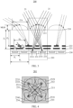
- FIGS. 3 to 5 show a schematic sectional view, a schematic top view and a schematic perspective view of a fingerprint identification apparatus 200, which does not fall under the scope of the claims.
- the fingerprint identification apparatus 200 is applied under a display screen to implement under-screen optical fingerprint identification, and the fingerprint identification apparatus 200 includes a plurality of fingerprint identification units 201 distributed in a square array. As shown in FIGS. 3 to 5 , in the fingerprint identification apparatus 200, each fingerprint identification unit 201 includes:
- a transmittance of each of the at least one light shielding layer to light of a specific wavelength band is less than a preset threshold (such as 20%) to avoid the corresponding light to pass through.
- a micro lens included in each fingerprint identification unit 201 of a plurality of fingerprint identification units in a fingerprint identification apparatus forms a micro lens array 210.
- a plurality of pixel unit included in each fingerprint identification unit 201 of the plurality of fingerprint identification units in the fingerprint identification apparatus form a pixel array 230.
- a light shielding layer in each fingerprint identification unit 201 is actually a local light shielding layer.
- the fingerprint identification apparatus in the embodiment of the present application will be introduced below with a fingerprint identification unit 201 as a unit, and the local light shielding layer in the fingerprint identification unit 201 is referred to as a light shielding layer for short.
- the fingerprint identification unit 201 includes a plurality of light shielding layers, that is, a bottom light shielding layer 221 and an intermediate light shielding layer 222, where the bottom light shielding layer 221 is a light shielding layer closest to the pixel unit, and the intermediate light shielding layer 222 is a light shielding layer other than the bottom light shielding layer.
- one micro lens corresponds to four pixel units.
- the fingerprint identification unit 201 in FIG. 3 is actually a sectional view of a fingerprint identification unit 201 in FIG. 5 along a line connecting a center of a first pixel unit 231 and a center of a third pixel unit 233
- FIG. 4 is a top view of FIG. 5 .
- a first pixel unit 231, a second pixel unit 232, a third pixel unit 233 and a fourth pixel unit 234 are correspondingly disposed below a first micro lens 211, and the four pixel units are respectively located at bottoms of light directing channels in four different directions.
- each pixel unit is provided with a photosensitive region (or Active Area, AA) for respectively receiving four fingerprint light signals passing through the four light directing channels and converting the fingerprint light signals into corresponding electrical signals.
- the photosensitive region may be a region where a photodiode in the pixel unit is located, that is, a region in the pixel unit that receives a light signal, and other regions in the pixel unit may be used for setting other circuits in the pixel unit and for arrangement of wiring between pixels.
- a first photosensitive region 2311 in the first pixel unit 231, a second photosensitive region 2321 in the second pixel unit 232, a third photosensitive region 2331 in the third pixel unit 233, and a fourth photosensitive region 2341 in the fourth pixel unit 234 are all disposed at the bottoms of the above light directing channels in four different directions.
- the four light directing channels corresponding to the first micro lens 211 are all provided with four light passing holes on both the bottom light shielding layer 221 and the intermediate light shielding layer 222, and the four light passing holes on each light shielding layer correspond to four pixel units. That is, the light passing holes of the four light guiding channels in the bottom light shielding layer 221 and the intermediate light shielding layer 222 respectively are independent of each other. For example, in FIG.
- the bottom light shielding layer 221 is provided with a light passing hole 2211 corresponding to the first pixel unit 231
- the intermediate light shielding layer 222 is provided with a light passing hole 2221 corresponding to the first pixel unit 231
- the light passing hole 2211 and the light passing hole 2221 are both light passing holes on the first light directing channel that is corresponding to the first pixel unit 231.
- the light passing hole 2211 and the light passing hole 2221 form a first light directing channel corresponding to the first pixel unit 231.
- a center of the light passing hole 2211 and a center of the light passing hole 2221 may be on a straight line, and a direction of the straight line is a direction of the first light directing channel.
- an oblique light signal 21 in a first direction passes through the first light directing channel to the first photosensitive region 2311 in the first pixel unit 231, while a light signal in another direction (for example, a light signal shown by a dotted line in the figure) is shielded in the light shielding layer and cannot be transmitted to the pixel unit.
- the above oblique light signal 21 in the first direction may be an oblique fingerprint light signal in the first direction that passes through the display screen and reaches the first micro lens 211 after being reflected or scattered by a finger above the display screen.
- the oblique light signal 21 in the first direction may be used to detect fingerprint information.
- the other pixel unit may also receive an oblique fingerprint light signal in another direction, and the oblique fingerprint light signal in another direction passes through a light directing channel formed by light passing holes, and is transmitted to the corresponding pixel unit after converged by the first micro lens 211.
- an oblique light signal 23 in a third direction reaches the third photosensitive region 2331 in the third pixel unit 233 through a third light directing channel.
- four light directing channels corresponding to each micro lens are provided with four light passing holes in the bottom light shielding layer 221, the four light passing holes correspond to four pixel units, and light passing holes of the four light directing channels on the intermediate light shielding layer 222 overlap, that is, only one light passing hole is provided in the intermediate light shielding layer 222.
- FIGS. 6 to 8 show a schematic sectional view, a schematic top view and a schematic perspective view of another fingerprint identification apparatus, which does not fall under the scope of the claims.
- a fingerprint identification unit 201 in FIG. 6 is actually a sectional view of a fingerprint identification unit 201 in FIG. 8 along a line connecting a center of a first pixel unit 231 and a center of a third pixel unit 233, and
- FIG. 7 is a top view of FIG. 8 .
- a bottom light shielding layer 221 is provided with a light passing hole 2211 corresponding to a first pixel unit 231
- an intermediate light shielding layer 222 is provided with one large light passing hole 2221
- the light passing hole 2221 corresponds to four pixel units.
- the light passing hole 2211 and the light passing hole 2221 form a first light directing channel corresponding to the first pixel unit 231.
- a center of the light passing hole 2211 and a center of the light passing hole 2221 may be on a straight line, and a direction of the straight line is a direction of the first light directing channel.
- an oblique light signal 21 in a first direction passes through the first light directing channel to a first photosensitive region 2311 in the first pixel unit 231, while a light signal in another direction (for example, a light signal shown by a dotted line in the figure) is shielded in the light shielding layer and cannot be transmitted to the pixel unit.
- a pixel array 230 in the fingerprint identification apparatus 200 may generate four fingerprint images based on the received light signals in four different directions, and then a fingerprint image with high resolution is obtained so as to improve a fingerprint identification effect.
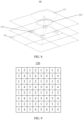
- FIG. 9 shows a schematic diagram of arrangement of a pixel array 230.
- " 1 " represents a pixel unit for receiving an oblique light signal in a first direction
- "2" represents a pixel unit for receiving an oblique light signal in a second direction
- "3 represents a pixel unit for receiving an oblique light signal in a third direction
- "4" represents a pixel unit for receiving an oblique light signal in a fourth direction.
- all the pixel units represented by "1" may be used to generate a first fingerprint image respectively, and all the pixel units represented by "2” may be used to generate a second fingerprint image respectively, all the pixel units represented by "3” may be used to generate a third fingerprint image respectively, and all the pixel units represented by "4" may be used to generate a fourth fingerprint image respectively, that is, a total of four fingerprint images may be generated.
- the four fingerprint images may be used for fingerprint identification independently, or may also be combined into a fingerprint image of high resolution, so as to improve an identification effect of a fingerprint identification apparatus.
- the four fingerprint images are generated by oblique light signals in different directions, the four fingerprint images correspond to different object-side imaging regions, and other applications such as expanding a size of an object-side field of view can also be realized.
- four pixel units corresponding to a single micro lens can receive light signals in four directions simultaneously, which increases an amount of light admitted to a fingerprint identification apparatus, reduces exposure time and increases a field of view.
- non-frontal light imaging that is, oblique light imaging
- FIGS. 11 and 12 show schematic sectional views of two fingerprint identification units 201 respectively
- FIGS. 13 to 15 are schematic top views of FIG. 11
- FIG. 16 which does not fall under the scope of the claims, is a schematic top view of FIG. 12 .
- light passing holes of four light directing channels in an intermediate light shielding layer 222 overlap, and are one large circular through hole.
- a hole of the intermediate light shielding layer may be made by a method such as lithography or coating. Since a circle is a simple pattern, a complete pattern can be obtained with lower lithography resolution regardless of whether it is exposed with a positive adhesive or a negative adhesive.
- light passing holes of four light directing channels in an intermediate light shielding layer 222 overlap, and are a rounded rectangular through hole.
- the rounded rectangular through hole can further reduce a stray light leakage region without substantially increasing difficulty in a process, and can be achieved no matter a positive adhesive, a negative adhesive or coating is adopted.
- FIG. 15 depicting an embodiment, which falls under the scope of the claims, light passing holes of four light directing channels in an intermediate light shielding layer 222 overlap, and are a petaloid through hole.
- the number of petals is four, and the petaloid through hole is composed of four overlapping holes, or four holes having intersection.
- the shape of the petal is formed by four holes overlapping with each other and is exactly like a petal.
- the shape of the hole may be a circle, an ellipse or other shapes.
- a fingerprint identification unit includes nine pixel units, that is, nine light directing channels
- the number of petals is nine
- the petaloid through hole is composed of nine overlapping light passing holes.
- the number of petals may be related to the number of pixel units included in a fingerprint identification unit.
- FIG. 15 shows petaloid light passing holes formed by four circular holes partially overlapping/intersecting with each other.
- the petaloid through hole Compared with the rounded rectangular through hole and the large circular through hole, the petaloid through hole has an advantage of further reducing unnecessary light leakage region, promoting collimation of incident light to the largest extent, and increasing image contrast, but higher lithography resolution is required, and costs will be increased if manufacturing is implemented by means of coating.
- light passing holes of four light directing channels in the intermediate light shielding layer 222 are independent of each other.
- D 2 may be defined as a light passing aperture of a light passing region formed by light passing holes in the intermediate light shielding layer 222 that are corresponding to the four pixel units, and the light passing aperture D 2 may be a distance between two farthest points in the light passing region on a plane where the intermediate light shielding layer is located.
- D 2 may be a diameter of the circle on the intermediate light shielding layer 222 as shown in FIG. 13 , a diagonal of the rounded rectangle on the intermediate light shielding layer 222 as shown in FIG. 14 , a largest size through a center of the petal on the intermediate light shielding layer 222 as shown in FIG. 15 , or the farthest distance between two diagonal holes on the intermediate light shielding layer 222 as shown in FIG. 16 .
- CA may further be defined as a maximum aperture of the micro lens 211, for example, CA may be a maximum width of the micro lens 211 in the maximum cross section in a horizontal direction.
- the micro lens 211 may be a spherical lens or an aspherical lens, of which an upper surface is spherical or aspherical, and a lower surface is a horizontal plane, and the maximum aperture CA of the micro lens 211 may be a maximum width of the lower surface.
- the micro lens 211 may be a spherical lens, of which a lower surface is a circular horizontal plane, and the maximum aperture CA of the micro lens 211 is a diameter of the circular horizontal plane.
- a shape of the light passing region of the intermediate light shielding layer 222 may also be a special shape as shown in FIG. 17 , which does not fall under the scope of the claims, that is, an irregular shape, and D 2 is defined as shown in the figure.
- a light passing aperture D 2 of the light passing region and a maximum aperture CA of the micro lens 211 satisfy 0.3 ⁇ D 2 /CA ⁇ 1.3. It can be understood that when the fingerprint identification apparatus includes a plurality of intermediate light shielding layers, any intermediate light shielding layer may satisfy the value range of D 2 /CA, as well as other parameter ranges related to the intermediate light shielding layer. It may also be that the plurality of intermediate light shielding layers all meet the related parameter ranges.
- FIG. 18 shows a curve graph of contrast and brightness of an image as a function of D 2 /CA.
- FIG. 19 shows a schematic diagram of images captured under three D 2 /CA constraints. It can be understood that image contrast characterizes a difference in the degree of brightness or darkness of an image, and may also be understood as a contrast ratio of an image.
- a light passing aperture D 2 of a light passing region in an intermediate light shielding layer and a maximum aperture CA of a micro lens may be constrained to satisfy 0.3 ⁇ D 2 /CA ⁇ 1.3. If D 2 /CA is too small, an amount of light admitted to the light passing region in the intermediate light shielding layer is less, which may cause an image to become darker and noise to increase; and if D 2 /CA is too large, it may cause stray light to enter, thereby affecting image sharpness. If D 2 /CA is within a range constrained by the present application, image aliasing can be effectively reduced during imaging, the imaging has higher contrast and higher brightness, and ultimately a better imaging effect for various objects can be achieved, and identification accuracy is improved.
- Z i may be defined as a depth between a lower surface of an i-th light shielding layer and a lower surface of the micro lens 211 from bottom to top.
- Z 1 is defined as a depth between a lower surface of the bottom light shielding layer 221 and the lower surface of the micro lens 211
- Z 2 is defined as a depth between a lower surface of the intermediate light shielding layer 222 and the lower surface of the micro lens 211.
- the depth Z 2 between the lower surface of the intermediate light shielding layer 222 and the lower surface of the micro lens 211 and the depth Z 1 between the lower surface of the bottom light shielding layer 221 and the lower surface of the micro lens 211 may also be constrained to satisfy 0.1 ⁇ Z 2 /Z 1 ⁇ 0.9.
- 0.1 ⁇ Z 2 /Z 1 ⁇ 0.9 is further constrained, that is, the intermediate light shielding layer is constrained from the size of the light passing region of the intermediate light shielding layer and the position of the intermediate light shielding layer between the bottom light shielding layer and the micro lens, which can effectively reduce stray light crosstalk, increase collimation of incident light, improve image contrast, and thus improve identification accuracy.
- one micro lens corresponds to four pixel units in a fingerprint identification unit 201.
- one micro lens may also correspond to two, three, or four or more pixel units, for example, nine, sixteen pixel units, etc.
- the embodiment of the present application does not limit the number of pixel units in the fingerprint identification unit.
- each fingerprint identification unit includes nine pixel units, that is, one micro lens corresponds to the nine pixel units
- the bottom light shielding layer may also include nine light passing holes, where one light passing hole of the bottom light shielding layer corresponds to one pixel unit.
- the intermediate light shielding layer only includes one light passing hole, that is, one micro lens corresponds to one light passing hole of the intermediate light shielding layer, and one light passing hole of the intermediate light shielding layer corresponds to the nine light passing holes of the bottom light shielding layer, and the nine light passing holes of the bottom light shielding layer are in one-to-one correspondence with the nine pixel units.
- the intermediate light shielding layer includes nine light passing holes, that is, one micro lens corresponds to the nine light passing holes of the intermediate light shielding layer, and the nine light passing holes of the intermediate light shielding layer are in one-to-one correspondence with the nine light passing holes of the bottom light shielding layer, and the nine light passing holes of the bottom light shielding layer are in one-to-one correspondence with the nine pixel units.
- each fingerprint identification unit includes sixteen pixel units, that is, one micro lens corresponds to the sixteen pixel units
- the bottom light shielding layer may also include sixteen light passing holes, where one light passing hole of the bottom light shielding layer corresponds to one pixel unit.
- the intermediate light shielding layer only includes one light passing hole, that is, one micro lens corresponds to one light passing hole of the intermediate light shielding layer, and one light passing hole of the intermediate light shielding layer corresponds to the sixteen light passing holes of the bottom light shielding layer, and the sixteen light passing holes of the bottom light shielding layer are in one-to-one correspondence with the sixteen pixel units.
- the intermediate light shielding layer includes sixteen light passing holes, that is, one micro lens corresponds to the sixteen light passing holes of the intermediate light shielding layer, and the sixteen light passing holes of the intermediate light shielding layer are in one-to-one correspondence with the sixteen light passing holes of the bottom light shielding layer, and the sixteen light passing holes of the bottom light shielding layer are in one-to-one correspondence with the sixteen pixel units.
- a shape of the light passing hole may be a circle, a rounded rectangle or a petal.
- A P b /P a , where P b is defined as an arrangement period of a plurality of micro lenses in the fingerprint identification apparatus, and P a is defined as an arrangement period of the plurality of pixel units in the fingerprint identification apparatus.
- the plurality of micro lenses form a micro lens array
- the plurality of pixel units form a pixel array
- an arrangement period of the plurality of micro lenses in both an X direction and a Y direction is P b
- an arrangement period of the plurality of pixel units in both the X direction and the Y direction is P a .
- the horizontal plane is parallel to a plane where the display screen is located
- a vertical plane is perpendicular to the plane where the display screen is located.
- D 1 is defined as a maximum aperture of each light passing hole in the bottom light shielding layer.
- D 1 represents a diameter of a light passing hole.
- D 1 represents a distance between opposite corners of a light passing hole.
- shapes of the plurality of light passing holes in the bottom light shielding layer may be the same or different.
- the shapes of the plurality of light passing holes in the bottom light shielding layer are the same, that is, the plurality of light passing holes may all be circular holes, rounded rectangular holes or rectangular holes.
- the shapes of the plurality of light passing holes in the bottom light shielding layer are different, that is, the plurality of light passing holes may include at least two of circular holes, rounded rectangular holes and rectangular holes.
- the micro lens 211 in the fingerprint identification unit 201 corresponds to four pixel units
- the micro lens 211 corresponds to four light passing holes of the bottom light shielding layer 221
- the four light passing holes may include three circular light passing holes and one rectangular hole, or four light passing holes may include three circular light passing holes and one rounded rectangular hole, or four light passing holes may include two circular light passing holes, one rectangular hole and one rounded rectangular hole, etc.
- the shapes of the four light passing holes may be combined arbitrarily, but by considering process complexity and process steps, the shapes of the light passing holes preferably remain the same.
- sizes of the plurality of light passing holes in the bottom light shielding layer may be the same or different.
- at least two of the plurality of light passing holes have different apertures.
- each of the plurality of light passing holes has the same aperture.
- the plurality of light passing holes in the bottom light shielding layer are circular holes of the same aperture.
- the light passing holes in the bottom light shielding layer are circular light passing holes, rounded rectangular holes or rectangular holes, which have good symmetry and have symmetrical light passing performance for light signals in various directions, so as to be able to improve balance of an image in various directions, and improve image quality.
- a maximum aperture D 1 of each light passing hole in the bottom light shielding layer 221 and a maximum aperture CAof the micro lens may be constrained to satisfy 0.02 ⁇ D 1 /CA ⁇ 0.4.
- a proportion of a light-receiving area of the micro lens to a size of the light passing hole is comprehensively considered.
- the proportion is less than or equal to 0.4, each light passing hole in the bottom light shielding layer under the current micro lens can well shield stray light transmitted by an adjacent micro lens and reduce image aliasing, thereby improving a contrast ratio of imaging or contrast of an image.
- the proportion is greater than or equal to 0.02, it is ensured that sufficient light signals can pass through each light passing hole in the bottom light shielding layer so as to ensure imaging brightness. Therefore, by adopting the solution of the embodiment of the present application, both image brightness and image contrast can be taken into account, thereby improving image quality and identification success rate.
- the number of pixel units corresponding to the micro lens in one fingerprint identification unit can be increased, so that a light signal converged by the micro lens can be more fully utilized, and a space sampling rate of the image can be improved, thereby improving the brightness and contrast of the image, but this method will cause increase in difficulty of a manufacturing process and increase in costs. Therefore, in the technical solution of the embodiment of the present application, on the basis of considering manufacturing processes and costs, parameters in the fingerprint identification apparatus are constrained to meet certain conditions, so that requirements of image brightness and contrast are met.
- a radius of curvature ROC of the micro lens 211 and the depth distance Z 1 between the lower surface of the bottom light shielding layer 221 and the lower surface of the micro lens 211 satisfy 0.25 ⁇ ROC/Z 1 ⁇ 0.75.
- target fingerprint light signals in each direction among target fingerprint light signals in multiple directions are all focused on respective light passing holes in the bottom light shielding layer, an imaging effect is optimal in this case, and image contrast is improved while image brightness is taken into account. Therefore, in the technical solution of the embodiment of the present application, by constraining a radius of curvature ROC of the micro lens and a depth distance Z 1 between a lower surface of the bottom light shielding layer and a lower surface of the micro lens to satisfy 0.25 ⁇ ROC/Z 1 ⁇ 0.75, and comprehensively considering a proportion of a focal point of the micro lens to a position of the bottom light shielding layer, each light passing hole in the bottom light shielding layer meets or is close to the above condition, so as to improve image quality and identification success rate.
- a radius of curvature of an aspheric lens also has its calculation method.
- ROC/Z 1 0.4 ⁇ ROC/Z 1 ⁇ 0.6.
- 0.47 ⁇ ROC/Z 1 ⁇ 0.49 0.7, 0.48 or 0.49, or ROC/Z 1 may also be any value between 0.47 and 0.49, which is not specifically limited in the embodiment of the present application.
- stray light crosstalk can be reduced. As shown in FIG. 21 , if Z 2 /Z 1 is too large or too small, the stray light crosstalk will be increased.
- the position of each light passing hole in each light shielding layer may be constrained as follows: 0 ⁇ S i /Z 1 ⁇ 1, preferably, in some embodiments, 0.2 ⁇ S i /Z 1 ⁇ 0.5, where S i represents an offset of each light passing hole in an i-th light shielding layer in the fingerprint identification unit from a center of projection of the micro lens on the i-th light shielding layer.
- S i represents an offset of each light passing hole in an i-th light shielding layer in the fingerprint identification unit from a center of projection of the micro lens on the i-th light shielding layer.
- Z i a depth distance between a lower surface of the i-th light shielding layer to a lower surface of the micro lens
- the offset S i of the center of each light passing hole in the i-th light shielding layer from the center of the projection of the micro lens on the i-th light shielding layer may be the same or different, which is not specifically limited in the embodiment of the present application.
- target fingerprint light signals in multiple directions are transmitted to the corresponding pixel units through the light passing holes of each of the plurality of light shielding layers more accurately, and a light signal in a non-target direction can be shielded, so that influence of stray light on imaging is reduced, and image quality is further improved.
- the constraint range of S 1 /Z 1 may also be adjusted, and then the constraint range of the ROC/Z 1 may be adjusted according to the constraint range of the S 1 /Z 1 .
- the position of the light passing hole in the bottom light shielding layer an angle of the desired target fingerprint light signal is adjusted, and then the radius of curvature of the micro lens and the depth distance between the lower surface of the bottom light shielding layer and the lower surface of the micro lens are adjusted, so that the fingerprint identification apparatus in the embodiment of the present application can receive oblique light signals of various angles while satisfying good imaging conditions, and thus is applicable to a wider range of application scenarios.
- the radius of curvature ROC of the micro lens and the depth distance Z 1 between the lower surface of the bottom light shielding layer and the lower surface of the micro lens may be constrained to satisfy 0.25 ⁇ ROC/Z 1 ⁇ 0.75, and the maximum aperture D 1 of each light passing hole in the bottom light shielding layer and the maximum aperture CA of the micro lens may be constrained to satisfy 0.02 ⁇ D 1 /CA ⁇ 0.4.
- parameters of the bottom light shielding layer and parameters of the intermediate light shielding layer may also be constrained to meet certain conditions at the same time, so that requirements for improving image brightness and contrast can be further accurately met, and image quality is optimized to a large extent.
- FIG. 22 shows a schematic sectional view of another fingerprint identification apparatus 200.
- a fingerprint identification unit 201 in addition to a micro lens 211 and its corresponding four pixel units, a bottom light shielding layer 221 and an intermediate light shielding layer 222, it further includes: a protective layer 241, and the protective layer 241 is located above the bottom light shielding layer 221.
- the bottom light shielding layer 221 may be integrated with the pixel unit, that is, the bottom light shielding layer and the pixel unit may be integrated in an interior of a fingerprint sensor chip of the fingerprint identification apparatus, and are internal components of the fingerprint sensor chip.
- the bottom light shielding layer 221 may be a metal wiring layer located above the pixel unit in the sensor chip, that is, the bottom light shielding layer may be a metal wiring layer of the pixel unit, and is configured to transmit an electrical signal, or the bottom light shielding layer 221 may also be another material layer with low visible light transmittance.
- the above protective layer 241 may also be a laminated structure in the sensor chip, which is formed on a surface of the sensor chip to protect the sensor chip from being polluted by external water vapor and particles that result in failure of sensor performance.
- the protective layer 241 includes, but is not limited to, oxide of silicon and/or nitride of silicon.
- the protective layer 241 is also a transparent material layer with high transmittance for a light signal. By setting height of the protective layer 241, a certain focusing distance can be provided for a pixel unit in the sensor chip.
- the intermediate light shielding layer 222 is disposed on an upper surface of the sensor chip, that is, disposed on an upper surface of the protective layer 241.
- This setting can reduce a distance between the bottom light shielding layer 221 and the intermediate light shielding layer 222, and improve light directing performance of a light directing channel formed in two light shielding layers.
- the intermediate light shielding layer 222 may be a light absorbing material of a black polymer to absorb most of the light signals in the environment.
- the fingerprint identification unit 201 further includes: a second transparent medium layer 242, and the second transparent medium layer 242 is disposed above the intermediate light shielding layer 222 and fills the light passing holes in the intermediate light shielding layer 222.
- the second transparent medium layer 242 is also a medium layer formed of an optically high transmittance material.
- the second transparent medium layer 242 may be formed above the intermediate light shielding layer 222 by a semiconductor spin coating process and a curing process and fills the light passing holes in the intermediate light shielding layer 222.
- a certain focusing distance can also be provided for the pixel units in the sensor chip.
- the fingerprint identification unit 201 further includes: an infrared filter layer 250 configured to cut infrared light and part of red light, prevent the infrared light and part of the red light from entering the pixel unit and affect an imaging effect.
- an infrared filter layer 250 configured to cut infrared light and part of red light, prevent the infrared light and part of the red light from entering the pixel unit and affect an imaging effect.
- infrared light in the environment is strong. If the strong infrared light enters the pixel unit, a signal of the pixel unit is easily caused to be saturated, and the infrared light easily penetrates a finger to form transmitted light of the finger. This part of the transmitted light will affect imaging of the finger reflected light in a normal fingerprint identification process.
- the infrared light has great influence on the fingerprint imaging, and the infrared filter layer is required for cutting and filtering.
- the infrared filter layer 250 includes a plurality of inorganic material layers, and the plurality of inorganic material layers may be formed by coating the second transparent medium layer 242 by a coating process, and the coating process includes, but is not limited to, a coating method such as physical vapor deposition (PVD).
- PVD physical vapor deposition
- the plurality of inorganic material layers may be a plurality of inorganic material layers alternately grown by titanium dioxide/silicon dioxide (TiO 2 /SiO 2 ), or a plurality of inorganic material layers alternatively grown by niobium pentoxide/silicon dioxide (Nb 2 O 5 /SiO 2 ), or may also be other organic or inorganic materials used to cut off infrared light signals, which are not limited in the embodiments of the present application.
- the fingerprint identification unit 201 further includes: a color filter layer 260, and the color filter layer 260 is disposed above the infrared filter layer 250 and is configured to pass a light signal of a target wavelength band and cut off a light signal in another non-target wavelength band other than the color light signal of the target wavelength band, and the color filter layer may be realized by a semiconductor photolithography process.
- the color filter layer includes, but is not limited to, a red filter layer, a blue filter layer, a green filter layer or a white filter layer, and is configured to transmit a red light signal, a blue light signal, a green light signal or a white light signal.
- the pixel unit in the fingerprint identification unit 201 receives the color light signal, which can be used to perform fingerprint anti-counterfeiting to determine true and false fingers. If the color filter layer is a white filter layer for transmitting a white light signal, the pixel unit in the fingerprint identification unit 201 receives a white light signal, which can be used to generate a fingerprint image for fingerprint identification. Therefore, the fingerprint identification apparatus provided by the embodiment of the present application can further perform fingerprint anti-counterfeiting judgment on the basis of fingerprint identification, so that a success rate of fingerprint identification is improved.
- the color filter layer may be configured to absorb a light signal reflected by the infrared filter layer below the color filter layer, prevent the reflected light signal from being received by human eyes through the display screen, so as to solve an appearance problem of an under-screen fingerprint identification apparatus.
- the color filter layer is a white filter layer
- the color filter layer here may be a transparent medium layer or another filter material that transmits visible light.
- the embodiment of the present application does not specifically limit the structure of the color filter layer.
- the fingerprint identification unit 201 further includes: a third transparent medium layer 243, and the third transparent medium layer 243 is disposed between the micro lens 211 and the color filter layer 260.
- the third transparent medium layer 243 is also a medium layer formed of an optically high transmittance material, which can be formed above the color filter layer 260 by a semiconductor spin coating process and a curing process. And by setting height of the third transparent medium layer 243, a certain focusing distance can be provided for a pixel unit in the sensor chip.
- the uppermost layer of the fingerprint identification unit 201 is the micro lens 211, a material of which is generally an optically transparent organic material. Size and shape of the micro lens 211 may be designed through a semiconductor lithography process, and formed through a thermal reflow process.
- the micro lens 211 may be a spherical micro lens or an aspherical micro lens.
- FIG. 23 shows a schematic sectional view of another fingerprint identification apparatus 200.
- a bottom light shielding layer 221 and an intermediate light shielding layer 222 in addition to the micro lens 211 and its corresponding four pixel units, it further includes: a protective layer 241, and the protective layer 241 is located above the bottom light shielding layer 221.
- the fingerprint identification unit 201 further includes: an infrared filter layer 250, and the infrared filter layer 250 is formed on a surface of the protective layer 241 and configured to cut an infrared light signal.
- the fingerprint identification unit 201 further includes: an adhesive layer 270 configured to connect the intermediate light shielding layer 222 and the infrared filter layer 250.
- the adhesive layer 270 may be an organic material layer of optically high transmittance coated on the infrared filter layer 250, which can be realized by a semiconductor spin coating process and a curing process.
- the adhesive layer 270 may be a flat transparent layer with a flat surface, so as to prevent warpage of the infrared filter layer 250 formed by a plurality of organic material layers from affecting flatness of the intermediate light shielding layer 222, and further prevent an imaging effect from being affected.
- a first transparent medium layer 244 is further formed above the intermediate light shielding layer 222.
- the first transparent medium layer 244 may be formed above the intermediate light shielding layer 222 through a semiconductor spin coating process and a curing process and fills the light passing holes in the intermediate light shielding layer 222.
- a certain focusing distance can be provided for a pixel unit in the sensor chip.
- the fingerprint identification unit 201 further includes: a color filter layer 260, and the color filter layer 260 is disposed above the first transparent medium layer 244 and connects the first transparent medium layer 244 and the micro lens 211.
- the color filter layer 260 is configured to transmit a light signal of a target wavelength band, and cut off a light signal of another non-target wavelength band other than the color light signal of the target wavelength band.
- the color filter layer includes, but is not limited to, a red filter layer, a blue filter layer, a green filter layer or a white filter layer for transmitting a red light signal, a blue light signal, a green light signal or a white light signal.
- Tables 1 and 2 show numerical values of the parameters and numerical values of the constraints in the fingerprint identification apparatus of several specific embodiments, where the unit of each parameter in Table 1 is micrometer ( ⁇ m), and the unit of P b parameter in Table 2 is ⁇ m.
- Example 1 Example 2
- Example 3 Example 4
- Example 5 Example 6
- Example 7 P a 10.50 14.00 11.50 10.00 10.00 12.50 7.50 P b 21.00 28.00 23.00 20.00 20.00 25.00 15.00 CA 16.15 21.85 18.50 19.00 19.50 23.50 14.50 MLH 4.20 5.80 4.80 5.00 6.10 8.90 3.00 ROC 9.86 13.19 11.31 11.53 10.84 12.21 10.26 Z 1 23.30 27.57 20.93 22.64 21.91 24.06 18.23 S1 8.20 9.62 7.51 7.60 6.05 10.08 5.09 D 1 2.38 2.70 2.18 2.40 2.00 2.70 1.84 Z 2 15.25 16.82 17.54 18.89 18.37 19.85 15.11 D 2 13.30 15.88 18.10 18.43 16.02 25.05 12.48
- Table 1 corresponds to the fingerprint identification unit 201 and the fingerprint identification apparatus 200 shown in FIG. 3 and FIG. 21 .
- Table 2 exemplarily presents calculated values of different constraints in various embodiments.
- Table 2 Constraints Example 1
- Example 2 Example 3
- Example 4 Example 5
- Example 6 Example 7 ROC/Z 1 0.42 0.48 0.54 0.51 0.49 0.51 0.56
- D 1 /CA 0.15 0.12 0.12 0.13 0.10 0.11 0.13
- S1/Z 1 0.35 0.35 0.36 0.34 0.28 0.42 0.28 P b 21.00 28.00 23.00 20.00 20.00 20.00 25.00 15.00 P b /P a 2.00 2.00 2.00 2.00 2.00 2.00 2.00 D 2 /CA 0.82 0.73 0.98 0.97 0.82 1.07 0.86 Z 2 /Z 1 0.65 0.61 0.84 0.83 0.84 0.82 0.83
- parameters in the fingerprint identification apparatus may also be designed by using constraint values involved in Table 2, instead of being limited to the specific parameters listed in various embodiments in Table 1.
- FIG. 24 shows a curve graph of contrast and brightness of an image captured by a fingerprint identification apparatus 200 as a function of a shape of a hole of an intermediate light shielding layer 222.
- image contrast and image brightness corresponding to the shape of the hole of the intermediate light shielding layer 222 are shown in Table 3.
- Table 3 Image contrast Image brightness Large circular through hole 84.70% 121.11% Rounded rectangular through hole 88.16% 116.31% Petaloid through hole 100% 100% Independent hole 104.85% 90.24%
- FIG. 25 shows a schematic diagram of captured images when a hole of intermediate light shielding layer is the above four types of shapes. It is obvious from FIGS. 24 and 25 that in a case of the same contrast, image brightness decreases sequentially from a large circular through hole to an independent hole. In a case of the same brightness, image contrast increases sequentially from a large circular through hole to an independent hole. However, all of the four hole shapes can obtain relatively clear images.
- sequence numbers of the foregoing processes do not mean execution sequences in various method embodiments of the present application.
- the execution sequences of the processes should be determined according to functions and internal logic of the processes, and should not be construed as any limitation on the implementation processes of the embodiments of the present application.
- an embodiment of the present application further provides an electronic device 500, and the electronic device may include a display screen 510 and the fingerprint identification apparatus 520 of the above embodiments of the present application, where the fingerprint identification apparatus is disposed under the display screen to implement under-screen optical fingerprint identification.
- the electronic device 500 may be any electronic device having a display screen.
- the display screen 510 may adopt a display screen having a self-emitting display unit, for example, an organic light-emitting diode (OLED) display screen or a micro light-emitting diode (Micro-LED) display screen.
- OLED organic light-emitting diode
- Micro-LED micro light-emitting diode
- the fingerprint identification apparatus 520 may use a display unit (that is, an OLED light source) of the OLED display screen 510 located in a fingerprint detection region as an excitation light source for optical fingerprint detection.
- the fingerprint identification apparatus 500 may also use an internal light source or an external light source to provide a light signal for fingerprint detection.
- the fingerprint identification apparatus 500 may be applied to a non-self-emitting display screen, such as a liquid crystal display screen or other passive light-emitting display screens.
- the disclosed system and apparatus may be implemented in other manners.
- the foregoing described apparatus embodiments are merely exemplary.
- division of the units is merely logical function division and there may be other division manners in practical implementation.
- multiple units or components may be combined or integrated into another system, or some features may be ignored or not executed.
- the displayed or discussed mutual coupling or direct coupling or communication connection may be indirect coupling or communication connection through some interfaces, apparatuses or units, and may also be electrical, mechanical, or connection in other forms.
- the units described as separate parts may or may not be physically separate, and parts displayed as units may or may not be physical units, may be located in one position, or may be distributed on multiple network units. Some or all of the units may be selected depending on actual requirements to achieve the objectives of the solutions of the embodiments of the present application.
- functional units in the embodiments of the present application may be integrated into one processing unit, or each unit may exist alone physically, or two or more units may be integrated into one unit.
- the integrated unit may be implemented in a form of hardware, or may be implemented in a form of a software functional unit.
- the integrated unit When the integrated unit is implemented in the form of a software functional unit and sold or used as an independent product, the integrated unit may be stored in a computer-readable storage medium.
- the computer software product is stored in a storage medium and includes several instructions for instructing a computer device (which may be a personal computer, a server, a network device, or the like) to perform all or some of the steps of the method described in the embodiments of the present application.
- the foregoing storage medium includes a variety of media capable of storing program codes, such as a USB disk, a mobile hard disk, a read-only memory (ROM), a random access memory (RAM), a magnetic disk, and an optical disk.
Landscapes
- Physics & Mathematics (AREA)
- General Physics & Mathematics (AREA)
- Engineering & Computer Science (AREA)
- Optics & Photonics (AREA)
- Human Computer Interaction (AREA)
- Multimedia (AREA)
- Theoretical Computer Science (AREA)
- Image Input (AREA)
- Measurement Of The Respiration, Hearing Ability, Form, And Blood Characteristics Of Living Organisms (AREA)
Claims (12)
- Fingerabdruck-Identifikationsgerät, wobei das Fingerabdruck-Identifikationsgerät unter einem Anzeigebildschirm angewandt wird, um optische Fingerabdruck-Identifikation unter einer Anzeige zu implementieren, und das Fingerabdruck-Identifikationsgerät eine Vielzahl von Fingerabdruck-Identifikationseinheiten (201) umfasst, die in einer Anordnung verteilt sind, und jede der Vielzahl von Fingerabdruck-Identifikationseinheiten (201) umfasst:eine Vielzahl von Bildpunkteinheiten (231, 232, 233, 234);eine Mikrolinse (211), angeordnet über der Vielzahl von Bildpunkteinheiten (231, 232, 233, 234), undeine Vielzahl von Lichtabschirmschichten (221, 222), angeordnet zwischen der Mikrolinse (211) und der Vielzahl von Bildpunkteinheiten (231, 232, 233, 234), wobei jede der Vielzahl von Lichtabschirmschichten (221, 222) mit Lichtdurchgangslöchern (2221, 2211) korrespondierend mit der Vielzahl von Bildpunkteinheiten (231, 232, 233, 234) versehen ist, um eine Vielzahl von Lichtlenkungskanälen in einer Eins-zu-eins-Korrespondenz mit der Vielzahl von Bildpunkteinheiten (231, 232, 233, 234) zu bilden;wobei die Vielzahl von Bildpunkteinheiten (231, 232, 233, 234) jeweils konfiguriert ist zum Empfangen einer Vielzahl von Fingerabdrucklichtsignalen, reflektiert oder gestreut von einem Finger über dem Anzeigebildschirm, konvergiert durch die Mikrolinse (211) und übertragen durch die Vielzahl von Lichtlenkungskanälen, und die Vielzahl von Fingerabdrucklichtsignalen verwendet wird, Fingerabdruckinformationen des Fingers für Fingerabdruckidentifikation zu detektieren;wobei die Vielzahl von Lichtabschirmschichten eine untere Lichtabschirmschicht (221) und eine zwischenliegende Lichtabschirmschicht (222) umfasst, die zwischenliegende Lichtabschirmschicht (222) eine andere Lichtabschirmschicht als die untere Lichtabschirmschicht (221) umfasst, eine Lichtdurchgangsöffnung D2 einer Lichtdurchgangsregion, gebildet durch Lichtdurchgangslöcher (2221) in der zwischenliegenden Lichtabschirmschicht, die mit der Vielzahl von Bildpunkteinheiten (231, 232, 233, 234) korrespondieren, und eine maximale Öffnung CA der Mikrolinse 0,3≤D2/CA≤1,3 erfüllen, und D2 eine Distanz zwischen zwei am weitesten voneinander entfernten Punkten in der Lichtdurchgangsregion auf einer Ebene, auf der sich die zwischenliegende Lichtabschirmschicht (222) befindet, ist;dadurch gekennzeichnet, dass die Tiefe Z2 zwischen der unteren Oberfläche der zwischenliegenden Lichtabschirmschicht (222) und der unteren Oberfläche der Mikrolinse (211) und die Tiefe Z1 zwischen der unteren Oberfläche der unteren Lichtabschirmschicht (221) und der unteren Oberfläche der Mikrolinse (211) 0,3≤Z2/Z1≤0,75 erfüllen und die Lichtdurchgangsöffnung D2 der Lichtdurchgangsregion und die maximale Öffnung CA der Mikrolinse 0,5≤D2/CA≤0,8 erfüllen und eine Form der Lichtdurchgangsregion ein Blütenblatt ist, wobei das Blütenblatt durch die Lichtdurchgangslöcher in der zwischenliegenden Lichtabschirmschicht (222), die sich gegeneinander teilweise überlappen oder überschneiden, gebildet wird und die Anzahl von Blütenblättern zu der Anzahl von Bildpunkteinheiten, die in einer Fingerabdruck-Identifikationseinheit (201) enthalten sind, in Beziehung steht.
- Fingerabdruck-Identifikationsgerät nach Anspruch 1, wobei eine maximale Öffnung D1 jedes Lichtdurchgangslochs in der unteren Lichtabschirmschicht und die maximale Öffnung CA der Mikrolinse 0,02≤D1/CA≤0,4 erfüllen.
- Fingerabdruck-Identifikationsgerät nach einem der Ansprüche 1 bis 2, wobei ein Krümmungsradius, ROC, der Mikrolinse und eine Tiefendistanz Z1 zwischen einer unteren Oberfläche der unteren Lichtabschirmschicht und einer unteren Oberfläche der Mikrolinse 0,25≤ROC/Z1≤0,75 erfüllen.
- Fingerabdruck-Identifikationsgerät nach einem der Ansprüche 1 bis 3, wobei eine Position jedes Lichtdurchgangslochs in einer i-ten Lichtabschirmschicht der Vielzahl von Lichtabschirmschichten von unten nach oben 0≤Si/Z1≤1 erfüllt, wobei Si eine Distanz zwischen einer Mitte jedes Lichtdurchgangslochs in der i-ten Lichtabschirmschicht und einer Projektionsmitte der Mikrolinse auf der i-ten Lichtabschirmschicht ist.
- Fingerabdruck-Identifikationsgerät nach einem der Ansprüche 1 bis 4, wobei jedes Lichtdurchgangsloch in der unteren Lichtabschirmschicht ein kreisförmiges Loch einer gleichen Größe ist und die untere Lichtabschirmschicht eine Metallverdrahtungsschicht auf einer Oberfläche der Vielzahl von Bildpunkteinheiten ist.
- Fingerabdruck-Identifikationsgerät nach einem der Ansprüche 1 bis 5, wobei eine Anordnungsperiode Pb von Mikrolinsen in dem Fingerabdruck-Identifikationsgerät und eine Anordnungsperiode Pa der Bildpunkteinheiten in dem Fingerabdruck-Identifikationsgerät 1<Pb/Pa≤4 erfüllen; und
eine Anordnungsperiode Pb von Mikrolinsen in dem Fingerabdruck-Identifikationsgerät 5 µm≤Pb≤40 um erfüllt. - Fingerabdruck-Identifikationsgerät nach einem der Ansprüche 1 bis 6,wobei die Fingerabdruck-Identifikationseinheit ferner umfasst: eine Schutzschicht; unddie Schutzschicht über der unteren Lichtabschirmschicht angeordnet ist und mit der unteren Lichtabschirmschicht und der Vielzahl von Bildpunkteinheiten integriert ist.
- Fingerabdruck-Identifikationsgerät nach Anspruch 7, wobei die Lichtdurchgangslöcher der Vielzahl von Lichtlenkungskanälen sich in der zwischenliegenden Lichtabschirmschicht überlappen.
- Fingerabdruck-Identifikationsgerät nach Anspruch 8, wobei die Fingerabdruck-Identifikationseinheit ferner umfasst: eine Infrarotfilterschicht, wobei die Infrarotfilterschicht eine Filterschicht ist, beschichtet und aufgewachsen auf einer Oberfläche eines Sensorchips, und konfiguriert ist zum Unterbrechen von Infrarotlicht;eine Klebeschicht, wobei die Klebeschicht eine flache transparente Schicht ist, beschichtet auf einer Oberfläche der Infrarotfilterschicht, und die zwischenliegende Lichtabschirmschicht über der Klebeschicht angeordnet ist;eine erste transparente mittlere Schicht, angeordnet über der zwischenliegenden Lichtabschirmschicht, und die die Lichtdurchgangslöcher in der zwischenliegenden Lichtabschirmschicht füllt; undeine Farbfilterschicht, angeordnet zwischen der Mikrolinse und der ersten transparenten mittleren Schicht, wobei die Farbfilterschicht eine Rotfilterschicht, eine Blaufilterschicht, eine Grünfilterschicht oder eine Weißfilterschicht umfasst.
- Fingerabdruck-Identifikationsgerät nach Anspruch 7, wobei Lichtdurchgangslöcher der Vielzahl von Lichtlenkungskanälen in der zwischenliegenden Lichtabschirmschicht unabhängig voneinander sind.
- Fingerabdruck-Identifikationsgerät nach Anspruch 10, wobei die zwischenliegende Lichtabschirmschicht auf einer oberen Oberfläche der Schutzschicht angeordnet ist; und
wobei die Fingerabdruck-Identifikationseinheit ferner umfasst:eine zweite transparente mittlere Schicht, angeordnet über der zwischenliegenden Lichtabschirmschicht, und die die Lichtdurchgangslöcher in der zwischenliegenden Lichtabschirmschicht füllt;eine Infrarotfilterschicht, wobei die Infrarotfilterschicht eine Filterschicht ist, beschichtet und aufgewachsen auf einer Oberfläche der zweiten transparenten mittleren Schicht, und die zum Unterbrechen von Infrarotlicht konfiguriert ist;eine Farbfilterschicht, angeordnet über der Infrarotfilterschicht, wobei die Farbfilterschicht eine Rotfilterschicht, eine Blaufilterschicht, eine Grünfilterschicht oder eine Weißfilterschicht umfasst; undeine dritte transparente mittlere Schicht, angeordnet zwischen der Mikrolinse und der Farbfilterschicht. - Elektronische Vorrichtung, umfassend:einen Anzeigebildschirm; unddas Fingerabdruck-Identifikationsgerät nach einem der Ansprüche 1 bis 11,wobei das Fingerabdruck-Identifikationsgerät unter dem Anzeigebildschirm angeordnet ist, um optische Fingerabdruck-Identifikation unter einer Anzeige zu implementieren.
Applications Claiming Priority (1)
| Application Number | Priority Date | Filing Date | Title |
|---|---|---|---|
| PCT/CN2021/085455 WO2022205476A1 (zh) | 2021-04-02 | 2021-04-02 | 指纹识别装置和电子设备 |
Publications (4)
| Publication Number | Publication Date |
|---|---|
| EP4089576A1 EP4089576A1 (de) | 2022-11-16 |
| EP4089576A8 EP4089576A8 (de) | 2023-01-11 |
| EP4089576A4 EP4089576A4 (de) | 2023-03-01 |
| EP4089576B1 true EP4089576B1 (de) | 2024-06-19 |
Family
ID=83455532
Family Applications (1)
| Application Number | Title | Priority Date | Filing Date |
|---|---|---|---|
| EP21912303.1A Active EP4089576B1 (de) | 2021-04-02 | 2021-04-02 | Fingerabdruckerkennungsvorrichtung und elektronische vorrichtung |
Country Status (3)
| Country | Link |
|---|---|
| EP (1) | EP4089576B1 (de) |
| KR (1) | KR102942052B1 (de) |
| WO (1) | WO2022205476A1 (de) |
Family Cites Families (5)
| Publication number | Priority date | Publication date | Assignee | Title |
|---|---|---|---|---|
| US20170140221A1 (en) * | 2015-11-13 | 2017-05-18 | Intel Corporation | Dual function camera for infrared and visible light with electrically-controlled filters |
| WO2021008088A1 (zh) * | 2019-07-12 | 2021-01-21 | 深圳市汇顶科技股份有限公司 | 指纹检测装置和电子设备 |
| KR102365607B1 (ko) * | 2019-11-01 | 2022-02-18 | 선전 구딕스 테크놀로지 컴퍼니, 리미티드 | 지문 검출 장치 및 전자 장치 |
| CN212625580U (zh) * | 2020-06-03 | 2021-02-26 | 格科微电子(上海)有限公司 | 光学指纹器件 |
| CN111598068B (zh) * | 2020-07-24 | 2020-11-20 | 深圳市汇顶科技股份有限公司 | 指纹识别装置和电子设备 |
-
2021
- 2021-04-02 KR KR1020227022470A patent/KR102942052B1/ko active Active
- 2021-04-02 EP EP21912303.1A patent/EP4089576B1/de active Active
- 2021-04-02 WO PCT/CN2021/085455 patent/WO2022205476A1/zh not_active Ceased
Also Published As
| Publication number | Publication date |
|---|---|
| EP4089576A1 (de) | 2022-11-16 |
| KR102942052B1 (ko) | 2026-03-19 |
| EP4089576A8 (de) | 2023-01-11 |
| EP4089576A4 (de) | 2023-03-01 |
| KR20220137881A (ko) | 2022-10-12 |
| WO2022205476A1 (zh) | 2022-10-06 |
Similar Documents
| Publication | Publication Date | Title |
|---|---|---|
| EP3839808B1 (de) | Fingerabdruck-erkennungsgerät und elektronisches gerät | |
| US11783619B2 (en) | Fingerprint identification apparatus and electronic device | |
| CN113065469B (zh) | 指纹识别装置和电子设备 | |
| EP3885969B1 (de) | Fingerabdruckerkennungsverfahren, fingerabdruckerkennungsvorrichtung und elektronische vorrichtung | |
| CN211375615U (zh) | 指纹识别装置和电子设备 | |
| WO2021072753A1 (zh) | 指纹检测装置和电子设备 | |
| CN211180842U (zh) | 指纹检测装置和电子设备 | |
| US11531430B2 (en) | Fingerprint detection apparatus and electronic device | |
| EP3789913B1 (de) | Fingerabdruckdetektor und elektronische vorrichtung | |
| KR20220073835A (ko) | 이미지 수집 광학 구조 및 생체 특징의 진위를 감별하는 방법과 전자 장치 | |
| WO2021168666A1 (zh) | 指纹识别装置和电子设备 | |
| CN112784721B (zh) | 指纹识别装置和电子设备 | |
| CN111095283A (zh) | 指纹检测装置和电子设备 | |
| CN210864757U (zh) | 指纹检测装置和电子设备 | |
| EP4089576A1 (de) | Fingerabdruckerkennungsvorrichtung und elektronische vorrichtung | |
| CN210605735U (zh) | 指纹检测装置和电子设备 | |
| WO2023024091A1 (zh) | 指纹识别装置和电子设备 |
Legal Events
| Date | Code | Title | Description |
|---|---|---|---|
| STAA | Information on the status of an ep patent application or granted ep patent |
Free format text: STATUS: UNKNOWN |
|
| STAA | Information on the status of an ep patent application or granted ep patent |
Free format text: STATUS: THE INTERNATIONAL PUBLICATION HAS BEEN MADE |
|
| PUAI | Public reference made under article 153(3) epc to a published international application that has entered the european phase |
Free format text: ORIGINAL CODE: 0009012 |
|
| STAA | Information on the status of an ep patent application or granted ep patent |
Free format text: STATUS: REQUEST FOR EXAMINATION WAS MADE |
|
| 17P | Request for examination filed |
Effective date: 20220704 |
|
| AK | Designated contracting states |
Kind code of ref document: A1 Designated state(s): AL AT BE BG CH CY CZ DE DK EE ES FI FR GB GR HR HU IE IS IT LI LT LU LV MC MK MT NL NO PL PT RO RS SE SI SK SM TR |
|
| RAP3 | Party data changed (applicant data changed or rights of an application transferred) |
Owner name: DIXTECH INNOVATION PTE. LTD. |
|
| REG | Reference to a national code |
Ref legal event code: R079 Free format text: PREVIOUS MAIN CLASS: G06K0009000000 Ref country code: DE Ref legal event code: R079 Ref document number: 602021014672 Country of ref document: DE Free format text: PREVIOUS MAIN CLASS: G06K0009000000 Ipc: G06V0040130000 |
|
| A4 | Supplementary search report drawn up and despatched |
Effective date: 20230130 |
|
| RIC1 | Information provided on ipc code assigned before grant |
Ipc: G02B 30/32 20200101ALN20230124BHEP Ipc: G02B 5/00 20060101ALI20230124BHEP Ipc: G02B 3/00 20060101ALI20230124BHEP Ipc: G06V 40/13 20220101AFI20230124BHEP |
|
| RAP1 | Party data changed (applicant data changed or rights of an application transferred) |
Owner name: HUI DING INTERNATIONAL PTE. LTD. |
|
| STAA | Information on the status of an ep patent application or granted ep patent |
Free format text: STATUS: EXAMINATION IS IN PROGRESS |
|
| 17Q | First examination report despatched |
Effective date: 20231106 |
|
| GRAP | Despatch of communication of intention to grant a patent |
Free format text: ORIGINAL CODE: EPIDOSNIGR1 |
|
| STAA | Information on the status of an ep patent application or granted ep patent |
Free format text: STATUS: GRANT OF PATENT IS INTENDED |
|
| RIC1 | Information provided on ipc code assigned before grant |
Ipc: G02B 30/32 20200101ALN20240314BHEP Ipc: G02B 5/00 20060101ALI20240314BHEP Ipc: G02B 3/00 20060101ALI20240314BHEP Ipc: G06V 40/13 20220101AFI20240314BHEP |
|
| RIC1 | Information provided on ipc code assigned before grant |
Ipc: G02B 30/32 20200101ALN20240315BHEP Ipc: G02B 5/00 20060101ALI20240315BHEP Ipc: G02B 3/00 20060101ALI20240315BHEP Ipc: G06V 40/13 20220101AFI20240315BHEP |
|
| GRAS | Grant fee paid |
Free format text: ORIGINAL CODE: EPIDOSNIGR3 |
|
| INTG | Intention to grant announced |
Effective date: 20240416 |
|
| RIC1 | Information provided on ipc code assigned before grant |
Ipc: G02B 30/32 20200101ALN20240408BHEP Ipc: G02B 5/00 20060101ALI20240408BHEP Ipc: G02B 3/00 20060101ALI20240408BHEP Ipc: G06V 40/13 20220101AFI20240408BHEP |
|
| GRAA | (expected) grant |
Free format text: ORIGINAL CODE: 0009210 |
|
| STAA | Information on the status of an ep patent application or granted ep patent |
Free format text: STATUS: THE PATENT HAS BEEN GRANTED |
|
| AK | Designated contracting states |
Kind code of ref document: B1 Designated state(s): AL AT BE BG CH CY CZ DE DK EE ES FI FR GB GR HR HU IE IS IT LI LT LU LV MC MK MT NL NO PL PT RO RS SE SI SK SM TR |
|
| REG | Reference to a national code |
Ref country code: GB Ref legal event code: FG4D |
|
| REG | Reference to a national code |
Ref country code: CH Ref legal event code: EP |
|
| REG | Reference to a national code |
Ref country code: DE Ref legal event code: R096 Ref document number: 602021014672 Country of ref document: DE |
|
| PG25 | Lapsed in a contracting state [announced via postgrant information from national office to epo] |
Ref country code: BG Free format text: LAPSE BECAUSE OF FAILURE TO SUBMIT A TRANSLATION OF THE DESCRIPTION OR TO PAY THE FEE WITHIN THE PRESCRIBED TIME-LIMIT Effective date: 20240619 |
|
| PG25 | Lapsed in a contracting state [announced via postgrant information from national office to epo] |
Ref country code: HR Free format text: LAPSE BECAUSE OF FAILURE TO SUBMIT A TRANSLATION OF THE DESCRIPTION OR TO PAY THE FEE WITHIN THE PRESCRIBED TIME-LIMIT Effective date: 20240619 Ref country code: FI Free format text: LAPSE BECAUSE OF FAILURE TO SUBMIT A TRANSLATION OF THE DESCRIPTION OR TO PAY THE FEE WITHIN THE PRESCRIBED TIME-LIMIT Effective date: 20240619 |
|
| REG | Reference to a national code |
Ref country code: LT Ref legal event code: MG9D |
|
| PG25 | Lapsed in a contracting state [announced via postgrant information from national office to epo] |
Ref country code: GR Free format text: LAPSE BECAUSE OF FAILURE TO SUBMIT A TRANSLATION OF THE DESCRIPTION OR TO PAY THE FEE WITHIN THE PRESCRIBED TIME-LIMIT Effective date: 20240920 |
|
| REG | Reference to a national code |
Ref country code: NL Ref legal event code: MP Effective date: 20240619 |
|
| PG25 | Lapsed in a contracting state [announced via postgrant information from national office to epo] |
Ref country code: LV Free format text: LAPSE BECAUSE OF FAILURE TO SUBMIT A TRANSLATION OF THE DESCRIPTION OR TO PAY THE FEE WITHIN THE PRESCRIBED TIME-LIMIT Effective date: 20240619 |
|
| PG25 | Lapsed in a contracting state [announced via postgrant information from national office to epo] |
Ref country code: NO Free format text: LAPSE BECAUSE OF FAILURE TO SUBMIT A TRANSLATION OF THE DESCRIPTION OR TO PAY THE FEE WITHIN THE PRESCRIBED TIME-LIMIT Effective date: 20240919 Ref country code: LV Free format text: LAPSE BECAUSE OF FAILURE TO SUBMIT A TRANSLATION OF THE DESCRIPTION OR TO PAY THE FEE WITHIN THE PRESCRIBED TIME-LIMIT Effective date: 20240619 Ref country code: HR Free format text: LAPSE BECAUSE OF FAILURE TO SUBMIT A TRANSLATION OF THE DESCRIPTION OR TO PAY THE FEE WITHIN THE PRESCRIBED TIME-LIMIT Effective date: 20240619 Ref country code: GR Free format text: LAPSE BECAUSE OF FAILURE TO SUBMIT A TRANSLATION OF THE DESCRIPTION OR TO PAY THE FEE WITHIN THE PRESCRIBED TIME-LIMIT Effective date: 20240920 Ref country code: FI Free format text: LAPSE BECAUSE OF FAILURE TO SUBMIT A TRANSLATION OF THE DESCRIPTION OR TO PAY THE FEE WITHIN THE PRESCRIBED TIME-LIMIT Effective date: 20240619 Ref country code: BG Free format text: LAPSE BECAUSE OF FAILURE TO SUBMIT A TRANSLATION OF THE DESCRIPTION OR TO PAY THE FEE WITHIN THE PRESCRIBED TIME-LIMIT Effective date: 20240619 Ref country code: RS Free format text: LAPSE BECAUSE OF FAILURE TO SUBMIT A TRANSLATION OF THE DESCRIPTION OR TO PAY THE FEE WITHIN THE PRESCRIBED TIME-LIMIT Effective date: 20240919 |
|
| PG25 | Lapsed in a contracting state [announced via postgrant information from national office to epo] |
Ref country code: NL Free format text: LAPSE BECAUSE OF FAILURE TO SUBMIT A TRANSLATION OF THE DESCRIPTION OR TO PAY THE FEE WITHIN THE PRESCRIBED TIME-LIMIT Effective date: 20240619 |
|
| REG | Reference to a national code |
Ref country code: AT Ref legal event code: MK05 Ref document number: 1696432 Country of ref document: AT Kind code of ref document: T Effective date: 20240619 |
|
| PG25 | Lapsed in a contracting state [announced via postgrant information from national office to epo] |
Ref country code: NL Free format text: LAPSE BECAUSE OF FAILURE TO SUBMIT A TRANSLATION OF THE DESCRIPTION OR TO PAY THE FEE WITHIN THE PRESCRIBED TIME-LIMIT Effective date: 20240619 |
|
| PG25 | Lapsed in a contracting state [announced via postgrant information from national office to epo] |
Ref country code: PT Free format text: LAPSE BECAUSE OF FAILURE TO SUBMIT A TRANSLATION OF THE DESCRIPTION OR TO PAY THE FEE WITHIN THE PRESCRIBED TIME-LIMIT Effective date: 20241021 |
|
| PG25 | Lapsed in a contracting state [announced via postgrant information from national office to epo] |
Ref country code: PT Free format text: LAPSE BECAUSE OF FAILURE TO SUBMIT A TRANSLATION OF THE DESCRIPTION OR TO PAY THE FEE WITHIN THE PRESCRIBED TIME-LIMIT Effective date: 20241021 |
|
| PG25 | Lapsed in a contracting state [announced via postgrant information from national office to epo] |
Ref country code: PL Free format text: LAPSE BECAUSE OF FAILURE TO SUBMIT A TRANSLATION OF THE DESCRIPTION OR TO PAY THE FEE WITHIN THE PRESCRIBED TIME-LIMIT Effective date: 20240619 |
|
| PG25 | Lapsed in a contracting state [announced via postgrant information from national office to epo] |
Ref country code: EE Free format text: LAPSE BECAUSE OF FAILURE TO SUBMIT A TRANSLATION OF THE DESCRIPTION OR TO PAY THE FEE WITHIN THE PRESCRIBED TIME-LIMIT Effective date: 20240619 |
|
| PG25 | Lapsed in a contracting state [announced via postgrant information from national office to epo] |
Ref country code: IS Free format text: LAPSE BECAUSE OF FAILURE TO SUBMIT A TRANSLATION OF THE DESCRIPTION OR TO PAY THE FEE WITHIN THE PRESCRIBED TIME-LIMIT Effective date: 20241019 Ref country code: AT Free format text: LAPSE BECAUSE OF FAILURE TO SUBMIT A TRANSLATION OF THE DESCRIPTION OR TO PAY THE FEE WITHIN THE PRESCRIBED TIME-LIMIT Effective date: 20240619 |
|
| PG25 | Lapsed in a contracting state [announced via postgrant information from national office to epo] |
Ref country code: CZ Free format text: LAPSE BECAUSE OF FAILURE TO SUBMIT A TRANSLATION OF THE DESCRIPTION OR TO PAY THE FEE WITHIN THE PRESCRIBED TIME-LIMIT Effective date: 20240619 |
|
| PG25 | Lapsed in a contracting state [announced via postgrant information from national office to epo] |
Ref country code: RO Free format text: LAPSE BECAUSE OF FAILURE TO SUBMIT A TRANSLATION OF THE DESCRIPTION OR TO PAY THE FEE WITHIN THE PRESCRIBED TIME-LIMIT Effective date: 20240619 Ref country code: SK Free format text: LAPSE BECAUSE OF FAILURE TO SUBMIT A TRANSLATION OF THE DESCRIPTION OR TO PAY THE FEE WITHIN THE PRESCRIBED TIME-LIMIT Effective date: 20240619 |
|
| PG25 | Lapsed in a contracting state [announced via postgrant information from national office to epo] |
Ref country code: SM Free format text: LAPSE BECAUSE OF FAILURE TO SUBMIT A TRANSLATION OF THE DESCRIPTION OR TO PAY THE FEE WITHIN THE PRESCRIBED TIME-LIMIT Effective date: 20240619 Ref country code: ES Free format text: LAPSE BECAUSE OF FAILURE TO SUBMIT A TRANSLATION OF THE DESCRIPTION OR TO PAY THE FEE WITHIN THE PRESCRIBED TIME-LIMIT Effective date: 20240619 |
|
| PG25 | Lapsed in a contracting state [announced via postgrant information from national office to epo] |
Ref country code: SM Free format text: LAPSE BECAUSE OF FAILURE TO SUBMIT A TRANSLATION OF THE DESCRIPTION OR TO PAY THE FEE WITHIN THE PRESCRIBED TIME-LIMIT Effective date: 20240619 Ref country code: SK Free format text: LAPSE BECAUSE OF FAILURE TO SUBMIT A TRANSLATION OF THE DESCRIPTION OR TO PAY THE FEE WITHIN THE PRESCRIBED TIME-LIMIT Effective date: 20240619 Ref country code: RO Free format text: LAPSE BECAUSE OF FAILURE TO SUBMIT A TRANSLATION OF THE DESCRIPTION OR TO PAY THE FEE WITHIN THE PRESCRIBED TIME-LIMIT Effective date: 20240619 Ref country code: PL Free format text: LAPSE BECAUSE OF FAILURE TO SUBMIT A TRANSLATION OF THE DESCRIPTION OR TO PAY THE FEE WITHIN THE PRESCRIBED TIME-LIMIT Effective date: 20240619 Ref country code: IS Free format text: LAPSE BECAUSE OF FAILURE TO SUBMIT A TRANSLATION OF THE DESCRIPTION OR TO PAY THE FEE WITHIN THE PRESCRIBED TIME-LIMIT Effective date: 20241019 Ref country code: ES Free format text: LAPSE BECAUSE OF FAILURE TO SUBMIT A TRANSLATION OF THE DESCRIPTION OR TO PAY THE FEE WITHIN THE PRESCRIBED TIME-LIMIT Effective date: 20240619 Ref country code: EE Free format text: LAPSE BECAUSE OF FAILURE TO SUBMIT A TRANSLATION OF THE DESCRIPTION OR TO PAY THE FEE WITHIN THE PRESCRIBED TIME-LIMIT Effective date: 20240619 Ref country code: CZ Free format text: LAPSE BECAUSE OF FAILURE TO SUBMIT A TRANSLATION OF THE DESCRIPTION OR TO PAY THE FEE WITHIN THE PRESCRIBED TIME-LIMIT Effective date: 20240619 Ref country code: AT Free format text: LAPSE BECAUSE OF FAILURE TO SUBMIT A TRANSLATION OF THE DESCRIPTION OR TO PAY THE FEE WITHIN THE PRESCRIBED TIME-LIMIT Effective date: 20240619 |
|
| PG25 | Lapsed in a contracting state [announced via postgrant information from national office to epo] |
Ref country code: IT Free format text: LAPSE BECAUSE OF FAILURE TO SUBMIT A TRANSLATION OF THE DESCRIPTION OR TO PAY THE FEE WITHIN THE PRESCRIBED TIME-LIMIT Effective date: 20240619 |
|
| REG | Reference to a national code |
Ref country code: DE Ref legal event code: R097 Ref document number: 602021014672 Country of ref document: DE |
|
| PG25 | Lapsed in a contracting state [announced via postgrant information from national office to epo] |
Ref country code: DK Free format text: LAPSE BECAUSE OF FAILURE TO SUBMIT A TRANSLATION OF THE DESCRIPTION OR TO PAY THE FEE WITHIN THE PRESCRIBED TIME-LIMIT Effective date: 20240619 |
|
| PLBE | No opposition filed within time limit |
Free format text: ORIGINAL CODE: 0009261 |
|
| STAA | Information on the status of an ep patent application or granted ep patent |
Free format text: STATUS: NO OPPOSITION FILED WITHIN TIME LIMIT |
|
| 26N | No opposition filed |
Effective date: 20250320 |
|
| PGFP | Annual fee paid to national office [announced via postgrant information from national office to epo] |
Ref country code: DE Payment date: 20250429 Year of fee payment: 5 |
|
| PGFP | Annual fee paid to national office [announced via postgrant information from national office to epo] |
Ref country code: FR Payment date: 20250429 Year of fee payment: 5 |
|
| PG25 | Lapsed in a contracting state [announced via postgrant information from national office to epo] |
Ref country code: SE Free format text: LAPSE BECAUSE OF FAILURE TO SUBMIT A TRANSLATION OF THE DESCRIPTION OR TO PAY THE FEE WITHIN THE PRESCRIBED TIME-LIMIT Effective date: 20240619 |
|
| REG | Reference to a national code |
Ref country code: CH Ref legal event code: H13 Free format text: ST27 STATUS EVENT CODE: U-0-0-H10-H13 (AS PROVIDED BY THE NATIONAL OFFICE) Effective date: 20251125 |
|
| PG25 | Lapsed in a contracting state [announced via postgrant information from national office to epo] |
Ref country code: LU Free format text: LAPSE BECAUSE OF NON-PAYMENT OF DUE FEES Effective date: 20250402 |
|
| PG25 | Lapsed in a contracting state [announced via postgrant information from national office to epo] |
Ref country code: MC Free format text: LAPSE BECAUSE OF FAILURE TO SUBMIT A TRANSLATION OF THE DESCRIPTION OR TO PAY THE FEE WITHIN THE PRESCRIBED TIME-LIMIT Effective date: 20240619 |
|
| GBPC | Gb: european patent ceased through non-payment of renewal fee |
Effective date: 20250402 |
|
| REG | Reference to a national code |
Ref country code: BE Ref legal event code: MM Effective date: 20250430 |
|
| PG25 | Lapsed in a contracting state [announced via postgrant information from national office to epo] |
Ref country code: GB Free format text: LAPSE BECAUSE OF NON-PAYMENT OF DUE FEES Effective date: 20250402 |
|
| PG25 | Lapsed in a contracting state [announced via postgrant information from national office to epo] |
Ref country code: BE Free format text: LAPSE BECAUSE OF NON-PAYMENT OF DUE FEES Effective date: 20250430 |
|
| PG25 | Lapsed in a contracting state [announced via postgrant information from national office to epo] |
Ref country code: CH Free format text: LAPSE BECAUSE OF NON-PAYMENT OF DUE FEES Effective date: 20250430 |
|
| PG25 | Lapsed in a contracting state [announced via postgrant information from national office to epo] |
Ref country code: IE Free format text: LAPSE BECAUSE OF NON-PAYMENT OF DUE FEES Effective date: 20250402 |