EP4088591A1 - Power supply unit of aerosol generating device - Google Patents
Power supply unit of aerosol generating device Download PDFInfo
- Publication number
- EP4088591A1 EP4088591A1 EP22172271.3A EP22172271A EP4088591A1 EP 4088591 A1 EP4088591 A1 EP 4088591A1 EP 22172271 A EP22172271 A EP 22172271A EP 4088591 A1 EP4088591 A1 EP 4088591A1
- Authority
- EP
- European Patent Office
- Prior art keywords
- board
- power source
- terminal
- mcu
- receptacle
- Prior art date
- Legal status (The legal status is an assumption and is not a legal conclusion. Google has not performed a legal analysis and makes no representation as to the accuracy of the status listed.)
- Granted
Links
Images









Classifications
-
- A—HUMAN NECESSITIES
- A24—TOBACCO; CIGARS; CIGARETTES; SIMULATED SMOKING DEVICES; SMOKERS' REQUISITES
- A24F—SMOKERS' REQUISITES; MATCH BOXES; SIMULATED SMOKING DEVICES
- A24F40/00—Electrically operated smoking devices; Component parts thereof; Manufacture thereof; Maintenance or testing thereof; Charging means specially adapted therefor
- A24F40/40—Constructional details, e.g. connection of cartridges and battery parts
-
- A—HUMAN NECESSITIES
- A24—TOBACCO; CIGARS; CIGARETTES; SIMULATED SMOKING DEVICES; SMOKERS' REQUISITES
- A24F—SMOKERS' REQUISITES; MATCH BOXES; SIMULATED SMOKING DEVICES
- A24F40/00—Electrically operated smoking devices; Component parts thereof; Manufacture thereof; Maintenance or testing thereof; Charging means specially adapted therefor
- A24F40/20—Devices using solid inhalable precursors
Definitions
- the present invention relates to a power source unit of an aeroslo generating device.
- a plurality of boards may be disposed in a case.
- JP-T-2020-531015 discloses that a main circuit board is disposed inside an aerosol generating device along a longitudinal direction, and a sub-circuit board is disposed above the main circuit board along a horizontal direction.
- the boards may come into contact with each other depending on a fixing method thereof or a usage environment of a user, which may cause a short circuit.
- the present invention provides a power source unit of an aerosol generating device capable of appropriately avoiding contact between boards in a case.
- a power source unit of an aerosol generating device including: a power source; a heater connector to which a heater configured to heat an aerosol source by consuming power supplied from the power source is connected; a first board; a second board separate from the first board; a case in which the power source, the heater connector, the first board, and the second board are housed; and a spacer disposed between the first board and the second board and configured to hold the first board and the second board in parallel.
- the suction system includes a non-combustion-type suction device 100 (hereinafter, also simply referred to as the "suction device 100") that is an embodiment of a power source unit of the present invention, and a rod 500 heated by the suction device 100.
- a configuration in which the suction device 100 undetachably houses a heating unit will be described as an example.
- the heating unit may be configured to be detachable from the suction device 100.
- a unit in which the rod 500 and the heating unit are integrated may be configured to be detachable from the suction device 100.
- the power source unit of an aerosol generating device may not include the heating unit as a constituent element.
- the term "undetachable” refers to a mode in which detachment cannot be performed as long as intended use is intended.
- the heating unit may be configured by cooperation of an induction heating coil provided in the suction device 100 and a susceptor incorporated in the rod 500.
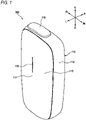
- Fig. 1 is a perspective view showing an overall configuration of the suction device 100.
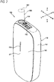
- Fig. 2 is a perspective view of the suction device 100 with the rod 500 attached.
- Fig. 3 is another perspective view of the suction device 100.
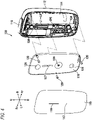
- Fig. 4 is an exploded perspective view of the suction device 100.
- a three-dimensional space orthogonal coordinate system is described in which three directions orthogonal to each other are referred to as a front-rear direction, a left-right direction, and an up-down direction for the sake of convenience.
- Fr denotes a front side
- Rr denotes a rear side
- R denotes a right side
- L denotes a left side
- U denotes an upper side
- D denotes a lower side.
- the suction device 100 is configured to generate aerosol containing flavor by heating the elongated, substantially cylindrical rod 500 (see Fig. 2 ) serving as an example of a flavor component generating base material having a filler containing an aerosol source, a flavor source, and the like.
- the rod 500 contains the filler containing the aerosol source that is heated at a predetermined temperature to generate the aerosol.
- a type of the aerosol source is not particularly limited, and extraction substances from various natural products and/or constituent components thereof can be selected according to an intended use.
- the aerosol source may be a solid, or may be, for example, a polyhydric alcohol such as glycerin or propylene glycol, or a liquid such as water.
- the aerosol source may contain the flavor source such as a cigarette raw material that releases a flavor component by heating or an extract derived from the cigarette raw material. Gas to which the flavor component is added is not limited to the aerosol, and for example, invisible steam may be generated.
- the filler of the rod 500 may contain cigarettes as the flavor source.
- a material of the cigarettes is not particularly limited, and known materials such as lamina and midbone can be used.
- the filler may contain one kind or two or more kinds of fragrances.
- a type of the fragrance is not particularly limited, and is preferably menthole from a viewpoint of imparting a good draft.
- the flavor source may contain a plant (for example, mint, Kampo, or herb) other than a cigarette. Depending on applications, the rod 500 may not include the flavor source.
- the suction device 100 includes a substantially rectangular parallelepiped case 110 having a front surface, a rear surface, a left surface, a right surface, an upper surface, and a lower surface.
- the case 110 includes a bottomed cylindrical case main body 112 in which the front surface, the rear surface, the upper surface, the lower surface, and the right surface are integrally formed, an outer panel 115 and an inner panel 118 that seal an opening 114 (see Fig. 4 ) of the case main body 112 and form the left surface, and a slider 119.
- the inner panel 118 is fixed to the case main body 112 by a bolt 120.
- the outer panel 115 is fixed to the case main body 112 so as to cover an outer surface of the inner panel 118 by magnets 124 held by a chassis 150 (see Fig. 5 ), which will be described later, housed in the case main body 112. Since the outer panel 115 is fixed by the magnets 124, a user can replace the outer panel 115 in accordance with his or her preference.
- the inner panel 118 is provided with two through holes 126 through which the magnets 124 penetrate.
- a vertically long hole 127 and a circular round hole 128 are further provided between the two through holes 126 disposed in the up-down direction.
- the long hole 127 is for transmitting light emitted from eight light emitting diodes (LEDs) L1 to L8 incorporated in the case main body 112.
- a button-type operation switch OPS incorporated in the case main body 112 passes through the round hole 128. Accordingly, the user can detect the light emitted from the eight LEDs L1 to L8 via an LED window 116 of the outer panel 115. Further, the user can press down the operation switch OPS via a pressing portion 117 of the outer panel 115.
- an opening 132 into which the rod 500 can be inserted is provided in the upper surface of the case main body 112.
- the slider 119 is coupled to the case main body 112 so as to be movable in the front-rear direction between a position (see Fig. 1 ) where the opening 132 is closed and a position (see Fig. 2 ) where the opening 132 is opened.
- the slider 119 is transparent and only an outer shape of the slider 119 is indicated by a two-dot chain line in order to facilitate understanding.
- the operation switch OPS is used to perform various operations of the suction device 100.
- the user operates the operation switch OPS via the pressing portion 117 in a state in which the rod 500 is inserted into and attached to the opening 132 as shown in Fig. 2 .
- the rod 500 is heated by a heating unit 170 (see Fig. 5 ) without being burned.
- the aerosol is generated from the aerosol source contained in the rod 500, and the flavor of the flavor source contained in the rod 500 is added to the aerosol.
- the user can suction the aerosol containing the flavor by holding a suction port 502 of the rod 500 protruding from the opening 132 in mouth and suctioning.
- a charging terminal 134 that is electrically connected to an external power source such as an outlet or a mobile battery to receive power supply is provided in the lower surface of the case main body 112.
- the charging terminal 134 is a universal serial bus (USB) Type-C receptacle, and is not limited thereto.
- the charging terminal 134 is hereinafter also referred to as a receptacle RCP.
- the charging terminal 134 may include, for example, a power receiving coil, and may be configured to receive electric power transmitted from the external power source in a non-contact manner.
- a power transmission (wireless power transfer) method may be an electromagnetic induction type, a magnetic resonance type, or a combination of the electromagnetic induction type and the magnetic resonance type.
- the charging terminal 134 can be connected to various USB terminals or the like, and may include the power receiving coil described above.
- the configuration of the suction device 100 shown in Figs. 1 to 4 is merely an example.
- the suction device 100 can be configured in various forms such that the gas to which the flavor component is imparted is generated from the rod 500 by holding the rod 500 and applying an action such as heating, and the user can suction the generated gas.
- FIG. 5 is a perspective view of the internal unit 140 of the suction device 100.
- Fig. 6 is an exploded perspective view of the internal unit 140 of Fig. 5 .
- Fig. 7 is a perspective view of the internal unit 140 from which a power source BAT and the chassis 150 are removed.
- Fig. 8 is another perspective view of the internal unit 140 from which the power source BAT and the chassis 150 are removed.
- the internal unit 140 housed in an internal space of the case 110 includes the chassis 150, the power source BAT, a circuit unit 160, the heating unit 170, a notification unit 180, and various sensors.
- the chassis 150 includes a plate-shaped chassis main body 151 that is disposed substantially at a center of the internal space of the case 110 in the front-rear direction and extends in the up-down direction and the front-rear direction, a plate-shaped front-rear dividing wall 152 that is disposed substantially at the center of the internal space of the case 110 in the front-rear direction and extends in the up-down direction and the left-right direction, a plate-shaped up-down dividing wall 153 that extends forward from substantially a center of the front-rear dividing wall 152 in the up-down direction, a plate-shaped chassis upper wall 154 that extends rearward from upper edge portions of the front-rear dividing wall 152 and the chassis main body 151, and a plate-shaped chassis lower wall 155 that extends rearward from lower edge portions of the front-rear dividing wall 152 and the chassis main body 151.
- a left surface of the chassis main body 151 is covered with the inner panel 118 and the outer panel 115 of the case
- a heating unit housing region 142 is defined and formed in an upper front portion by the chassis 150, a board housing region 144 is defined and formed in a lower front portion, and a power source housing space 146 is defined and formed in a rear portion along the up-down direction.
- the heating unit 170 housed in the heating unit housing region 142 is constituted by a plurality of cylindrical members, and the plurality of cylindrical members are concentrically arranged to form a cylindrical body as a whole.
- the heating unit 170 includes a rod housing portion 172 capable of housing a part of the rod 500 therein, and a heater HTR (see Figs. 10 to 16 ) that heats the rod 500 from an outer periphery or a center of the rod 500. It is preferable that a surface of the rod housing portion 172 and the heater HTR are insulated from each other by forming the rod housing portion 172 with a heat insulating material or providing the heat insulating material inside the rod housing portion 172.
- the heater HTR is an element capable of heating the rod 500.
- the heater HTR is, for example, a heating element.
- the heating element include a heating resistor, a ceramic heater, and an induction heating type heater.
- a heater having a positive temperature coefficient (PTC) characteristic in which a resistance value increases with an increase in temperature is preferably used.
- the heater HTR having a negative temperature coefficient (NTC) characteristic in which the resistance value decreases with the increase in temperature may be used.
- the heating unit 170 has a function of defining a flow path of air to be supplied to the rod 500 and a function of heating the rod 500.
- the case 110 is formed with a vent (not shown) through which the air flows in, and is configured such that the air can flow into the heating unit 170.
- the power source BAT housed in the power source housing space 146 is a rechargeable secondary battery, an electric double layer capacitor, or the like, and is preferably a lithium ion secondary battery.
- An electrolyte of the power source BAT may one or a combination of a gel electrolyte, an electrolytic solution, a solid electrolyte, and an ionic liquid.
- the notification unit 180 notifies various kinds of information such as a state of charge (SOC) indicating a charging state of the power source BAT, a preheating time at a time of suction, and a suction possible period.
- the notification unit 180 includes the eight LEDs L1 to L8 and a vibration motor M.
- the notification unit 180 may include a light emitting element such as the LEDs L1 to L8, may include a vibration element such as the vibration motor M, or may include a sound output element.
- the notification unit 180 may be a combination of two or more of the light emitting element, the vibration element, and the sound output element.
- the various sensors include an intake sensor that detects a puff operation (suction operation) of the user, a power source temperature sensor that detects a temperature of the power source BAT, a heater temperature sensor that detects a temperature of the heater HTR, a case temperature sensor that detects a temperature of the case 110, a cover position sensor that detects a position of the slider 119, a panel detection sensor that detects attachment and detachment of the outer panel 115, and the like.
- the intake sensor mainly includes, for example, a thermistor T2 disposed in the vicinity of the opening 132.
- the power source temperature sensor mainly includes, for example, a thermistor T1 disposed in the vicinity of the power source BAT.
- the heater temperature sensor mainly includes, for example, a thermistor T3 disposed in the vicinity of the heater HTR.
- the rod housing portion 172 is preferably insulated from the heater HTR.
- the thermistor T3 is preferably in contact with or close to the heater HTR inside the rod housing portion 172.
- the heater HTR has the PTC characteristic or the NTC characteristic, the heater HTR itself may be used as the heater temperature sensor.
- the case temperature sensor mainly includes, for example, a thermistor T4 disposed in the vicinity of the left surface of the case 110.
- the cover position sensor mainly includes a Hall IC 14 (see Figs. 10 to 16 ) including a Hall element disposed in the vicinity of the slider 119.
- the panel detection sensor mainly includes a Hall IC 13 (see Figs. 10 to 16 ) including a Hall element disposed in the vicinity of an inner surface of the inner panel 118.
- the circuit unit 160 includes four circuit boards, a plurality of integrate circuits (ICs), and a plurality of elements.
- the four circuit boards include an MCU-mounted board 161 on which a micro controller unit (MCU) 1 and a charging IC 2 to be described later are mainly disposed, a receptacle-mounted board 162 on which the charging terminal 134 is mainly disposed, an LED-mounted board 163 on which the operation switch OPS, the LEDs L1 to L8, and a communication IC 15 to be described later are disposed, and a Hall IC-mounted board 164 on which the Hall IC 14 to be described later including the Hall element constituting the cover position sensor is disposed.
- the MCU-mounted board 161 and the receptacle-mounted board 162 are arranged parallel to each other in the board housing region 144. Specifically, the MCU-mounted board 161 and the receptacle-mounted board 162 are arranged such that respective element arrangement surfaces thereof are arranged along the left-right direction and the up-down direction, and the MCU-mounted board 161 is arranged in front of the receptacle-mounted board 162.
- the MCU-mounted board 161 and the receptacle-mounted board 162 are provided with openings 175 and 176 (see Figs. 17 to 20 ), respectively.
- the MCU-mounted board 161 and the receptacle-mounted board 162 are fixed to the chassis 150 with a bolt 136 in a state in which a spacer 173 is interposed between opening peripheral edge portions 166 and 168 of the opening portions 175 and 176.
- Fig. 22 is a perspective view of the spacer 173.
- the spacer 173 includes a large diameter portion 191, a first small diameter portion 192a that is provided on one end side of the large diameter portion 191 and has a smaller diameter than that of the large diameter portion 191, a second small diameter portion 192b that is provided on the other end side of the large diameter portion 191 and has a smaller diameter than that of the large diameter portion 191, a first disk portion 193a that connects one end of the large diameter portion 191 and the first small diameter portion 192a, a second disk portion 193b that connects the other end of the large diameter portion 191 and the second small diameter portion 192b, and a through hole 194 that is formed across the first small diameter portion 192a, the large diameter portion 191, and the second small diameter portion 192b, and has a cylindrical shape as a whole.
- the first disk portion 193a and the second disk portion 193b are formed parallel to each other.
- the bolt 136 is inserted through the opening 175 of the MCU-mounted board 161, the through hole 194 of the cylindrical spacer 173, and the opening 176 of the receptacle-mounted board 162, and is fixed to a board fixing portion 156 of the front-rear dividing wall 152 disposed between the MCU-mounted board 161 and the receptacle-mounted board 162 and the power source BAT in the front-rear direction with the spacer 173 interposed therebetween.
- the first small diameter portion 192a is fitted into and connected to the opening 175 of the MCU-mounted board 161
- the second small diameter portion 192b is fitted into and connected to the opening 176 of the receptacle-mounted board 162.
- the first disk portion 193a comes into contact with the opening peripheral edge portion 166 (see Fig. 20 ) of a secondary surface 161b of the MCU-mounted board 161, and the second disk portion 193b comes into contact with the opening peripheral edge portion 168 (see Fig. 17 ) of a primary surface 162a of the receptacle-mounted board 162. Accordingly, the MCU-mounted board 161 and the receptacle-mounted board 162 are held in parallel by the spacer 173.
- the spacer 173 is a holding member that is disposed between the MCU-mounted board 161 and the receptacle-mounted board 162 and holds the MCU-mounted board 161 and the receptacle-mounted board 162 in parallel.
- the spacer 173 is a holding member that is disposed between the MCU-mounted board 161 and the receptacle-mounted board 162 and holds the MCU-mounted board 161 and the receptacle-mounted board 162 in parallel.
- the two boards 161 and 162 held in parallel can ensure an electrically safe region SP in the case 110, and the internal space of the case 110 can be effectively used.
- a width (a length in the front-rear direction) of the region SP is equal to a length of the large diameter portion 191 of the spacer 173.
- the spacer 173 has conductivity, and grounds of the MCU-mounted board 161 and the receptacle-mounted board 162 are connected via the spacer 173. More specifically, the first small diameter portion 192a fitted into the opening 175 of the MCU-mounted board 161 is connected to the ground inside the MCU-mounted board 161, and the second small diameter portion 192b fitted into the opening 176 of the receptacle-mounted board 162 is connected to the ground inside the receptacle-mounted board 162. Accordingly, ground potentials of the MCU-mounted board 161 and the receptacle-mounted board 162 can be equalized, and supply of charging power and operating power and communication between the MCU-mounted board 161 and the receptacle-mounted board 162 can be stabilized. Further, since a volume of the spacer 173 can be freely set, a resistance can be reduced by making the spacer 173 thick and short.
- the secondary surface 161b of the MCU-mounted board 161 and the primary surface 162a of the receptacle-mounted board 162 face each other with a predetermined gap therebetween, thereby forming the electrically safe region SP described above.
- the primary surface 161a of the MCU-mounted board 161 faces the front surface of the case 110
- the secondary surface 162b of the receptacle-mounted board 162 faces the front-rear dividing wall 152 of the chassis 150.
- the MCU-mounted board 161 and the receptacle-mounted board 162 are electrically connected to each other via a flexible wiring board 165.
- the flexible wiring board 165 that electrically connects the MCU-mounted board 161 and the receptacle-mounted board 162 connects FPC connection portions 231 and 232 of the MCU-mounted board 161 and the receptacle-mounted board 162 to each other (see Figs. 17 to 20 ).
- Elements and ICs mounted on the MCU-mounted board 161 and the receptacle-mounted board 162 will be described later.
- the LED-mounted board 163 is disposed on a left side surface of the chassis main body 151 and between the two magnets 124 disposed in the up-down direction.
- An element arrangement surface of the LED-mounted board 163 is disposed along the up-down direction and the front-rear direction.
- the element arrangement surface of each of the MCU-mounted board 161 and the receptacle-mounted board 162 is orthogonal to the element arrangement surface of the LED-mounted board 163.
- the element arrangement surface of each of the MCU-mounted board 161 and the receptacle-mounted board 162 and the element arrangement surface of the LED-mounted board 163 are not limited to be orthogonal to each other, and preferably intersect with each other (are not parallel to each other).
- the vibration motor M constituting the notification unit 180 together with the LEDs L1 to L8 is fixed to a lower surface of the chassis lower wall 155 and is electrically connected to the MCU-mounted board 161.
- the Hall IC-mounted board 164 is disposed on an upper surface of the chassis upper wall 154.
- Fig. 9 is a schematic diagram showing operation modes of the suction device 100.
- the operation modes of the suction device 100 include a charging mode, a sleep mode, an active mode, a heating initial setting mode, a heating mode, and a heating completion mode.
- the sleep mode is a mode in which power saving is achieved by mainly stopping power supply to electrical components necessary for heating control of the heater HTR.
- the active mode is a mode in which most of functions other than heating control of the heater HTR are enabled.
- the suction device 100 switches the operation mode to the active mode.
- the suction device 100 switches the operation mode to the sleep mode.
- the heating initial setting mode is a mode in which an initial setting of control parameters and the like for starting heating control of the heater HTR is performed.
- the suction device 100 detects an operation of the operation switch OPS while operating in the active mode, the suction device 100 switches the operation mode to the heating initial setting mode, and when the initial setting is finished, the suction device 100 switches the operation mode to the heating mode.
- the heating mode is a mode in which the heating control (heating control for aerosol generation and heating control for temperature detection) of the heater HTR is executed.
- the suction device 100 starts the heating control of the heater HTR.
- the heating completion mode is a mode in which processing (processing of storing a heating history or the like) of completing the heating control of the heater HTR is executed.
- processing processing of storing a heating history or the like
- the suction device 100 switches the operation mode to the heating completion mode, and when the completion processing is completed, the suction device 100 switches the operation mode to the active mode.
- the suction device 100 switches the operation mode to the heating completion mode when a USB connection is made while operating in the heating mode, and when the completion processing is completed, switches the operation mode to the charging mode. As shown in Fig.
- the operation mode may be switched to the active mode before the operation mode is switched to the charging mode.
- the suction device 100 may switch the operation mode in an order of the heating completion mode, the active mode, and the charging mode.
- the charging mode is a mode in which the power source BAT is charged with power supplied from the external power source connected to the receptacle RCP.
- the suction device 100 switches the operation mode to the charging mode.
- the suction device 100 switches the operation mode to the sleep mode.
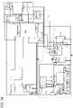
- Fig. 10 is a diagram showing a schematic configuration of an electric circuit of the internal unit 140. Fig. 10 only shows main elements and ICs.
- a wire indicated by a thick solid line in Fig. 10 is a wire (a wire connected to a ground provided in the internal unit 140) having the same potential as a reference potential (ground potential) of the internal unit 140, and this wire is hereinafter referred to as a ground line.
- electrical components obtained by chipping a plurality of circuit elements are indicated by rectangles, and reference numerals of various terminals are described inside the rectangles.
- a power source terminal VCC and a power source terminal VDD mounted on the chip indicate power source terminals on a high potential side, respectively.
- a power source terminal VSS and a ground terminal GND mounted on the chip are power source terminals on a low potential side (reference potential side), respectively.
- a difference between a potential of the power source terminal on the high potential side and a potential of the power source terminal on the low potential side is a power source voltage.
- the chipped electrical component executes various functions using the power source voltage.
- the MCU-mounted board 161 is provided with, as main electric components, an MCU 1 that performs overall control of the entire suction device 100, the charging IC 2 that performs charging control of the power source BAT, a load switch (hereinafter, LSW) 3 configured by combining a capacitor, a resistor, a transistor, and the like, and a voltage dividing circuit Pc for USB connection detection.
- LSW load switch
- the ground terminal GND of each of the charging IC 2 and the LSW 3 is connected to the ground line.
- the LED-mounted board 163 is provided with, as main electric components, the Hall IC 13 including a Hall element constituting the panel detection sensor, the LEDs L1 to L8, the operation switch OPS, and the communication IC 15.
- the communication IC 15 is a communication module for communicating with an electronic device such as a smartphone.
- Each of the power source terminal VSS of the Hall IC 13 and the ground terminal GND of the communication IC 15 is connected to the ground line.
- the communication IC 15 and the MCU 1 can communicate with each other through a communication line LN.
- One end of the operation switch OPS is connected to the ground line, and the other end of the operation switch OPS is connected to a terminal P4 of the MCU 1.
- the receptacle-mounted board 162 is provided with, as main electric components, a power source connector (in the drawing, the power source BAT connected to the power source connector is described) electrically connected to the power source BAT, a step-up DC/DC converter 9 (in the drawing, the step-up DC/DC 9 is described), a protection IC 10, an overvoltage protection IC 11, the receptacle RCP, switches S3 and S4 constituted by MOSFETs, an operational amplifier OP1, and a pair of (positive electrode side and negative electrode side) heater connectors Cn electrically connected to the heater HTR.
- a power source connector in the drawing, the power source BAT connected to the power source connector is described
- a step-up DC/DC converter 9 in the drawing, the step-up DC/DC 9 is described
- a protection IC 10 an overvoltage protection IC 11
- the receptacle RCP switches S3 and S4 constituted by MOSFETs
- an operational amplifier OP1 an operational amplifier
- the two ground terminals GND of the receptacle RCP, the ground terminal GND of the step-up DC/DC converter 9, the power source terminal VSS of the protection IC 10, the ground terminal GND of the overvoltage protection IC 11, and a negative power source terminal of the operational amplifier OP1 are each connected to the ground line.
- the Hall IC 14 including the Hall element constituting the cover position sensor is provided on the Hall IC-mounted board 164.
- the power source terminal VSS of the Hall IC 14 is connected to the ground line.
- An output terminal OUT of the Hall IC 14 is connected to a terminal P8 of the MCU 1.
- the MCU 1 detects opening and closing of the slider 119 based on a signal input to the terminal P8.
- Two power input terminals V BUS of the receptacle RCP are connected to an input terminal IN of the overvoltage protection IC 11 via a protection element such as a fuse Fs.
- a USB voltage V USB is supplied to two power input terminals V BUS of the receptacle RCP.
- the input terminal IN of the overvoltage protection IC 11 is connected to one end of a voltage dividing circuit Pa including a series circuit of two resistors.
- the other end of the voltage dividing circuit Pa is connected to the ground line.
- a connection point of the two resistors constituting the voltage dividing circuit Pa is connected to a voltage detection terminal OVLo of the overvoltage protection IC 11.
- the overvoltage protection IC 11 When a voltage input to the voltage detection terminal OVLo is less than a threshold, the overvoltage protection IC 11 outputs a voltage input to the input terminal IN from the output terminal OUT.
- the overvoltage protection IC 11 stops the voltage output from the output terminal OUT (cuts off the electrical connection between the LSW 3 and the receptacle RCP), thereby protecting the electrical components downstream of the overvoltage protection IC 11.
- the output terminal OUT of the overvoltage protection IC 11 is connected to an input terminal VIN of the LSW 3 and one end of the voltage dividing circuit Pc (the series circuit of two resistors) connected to the MCU 1.
- the other end of the voltage dividing circuit Pc is connected to the ground line.
- a connection point of the two resistors constituting the voltage dividing circuit Pc is connected to a terminal P17 of the MCU 1.
- One end of a voltage dividing circuit Pf including a series circuit of two resistors is connected to the input terminal VIN of the LSW 3.
- the other end of the voltage dividing circuit Pf is connected to the ground line.
- a connection point of the two resistors constituting the voltage dividing circuit Pf is connected to a control terminal ON of the LSW 3.
- a collector terminal of a bipolar transistor S2 is connected to the control terminal ON of the LSW 3.
- An emitter terminal of the bipolar transistor S2 is connected to the ground line.
- a base terminal of the bipolar transistor S2 is connected to a terminal P19 of the MCU 1.
- the MCU 1 turns on the bipolar transistor S2 while the USB connection is not made. Accordingly, since the control terminal ON of the LSW 3 is connected to the ground line via the bipolar transistor S2, a low-level signal is input to the control terminal ON of the LSW 3.
- the bipolar transistor S2 connected to the LSW 3 is turned off by the MCU 1 when the USB connection is made.
- the USB voltage V USB divided by the voltage dividing circuit Pf is input to the control terminal ON of the LSW 3. Therefore, when the USB connection is made and the bipolar transistor S2 is turned off, a high-level signal is input to the control terminal ON of the LSW 3. Accordingly, the LSW 3 outputs the USB voltage V USB supplied from the USB cable from the output terminal VOUT.
- a positive electrode terminal of the power source BAT is connected to the power source terminal VDD of the protection IC 10, the input terminal VIN of the step-up DC/DC converter 9, and a charging terminal bat of the charging IC 2. Therefore, a power source voltage V BAT of the power source BAT is supplied to the protection IC 10, the charging IC 2, and the step-up DC/DC converter 9.
- a resistor Ra, a switch Sa constituted by an MOSFET, and a switch Sb constituted by an MOSFET are connected in series in this order to a negative electrode terminal of the power source BAT.
- a current detection terminal CS of the protection IC 10 is connected to a connection point between the resistor Ra and the switch Sa.
- a control terminal of each of the switches Sa and Sb is connected to the protection IC 10.
- the protection IC 10 acquires a value of a current flowing through the resistor Ra at a time of charging and discharging of the power source BAT from a voltage input to the current detection terminal CS, and when the current value is excessive (in a case of an overcurrent), the protection IC 10 performs opening and closing control of the switch Sa and the switch Sb to stop charging or discharging of the power source BAT, thereby protecting the power source BAT. More specifically, when the protection IC 10 acquires the excessive current value at the time of charging the power source BAT, the protection IC 10 stops the charging of the power source BAT by turning off the switch Sb.
- the protection IC 10 When the protection IC 10 acquires the excessive current value at the time of discharging the power source BAT, the protection IC 10 stops the discharging of the power source BAT by turning off the switch Sa. Further, when a voltage value of the power source BAT is abnormal (in a case of overcharge or overvoltage) from the voltage input to the power source terminal VDD, the protection IC 10 performs opening and closing control of the switch Sa and the switch Sb to stop charging or discharging of the power source BAT, thereby protecting the power source BAT. More specifically, when the protection IC 10 detects the overcharge of the power source BAT, the protection IC 10 stops the charging of the power source BAT by turning off the switch Sb. When the protection IC 10 detects the overdischarge of the power source BAT, the protection IC 10 stops the discharge of the power source BAT by turning off the switch Sa.
- One end of a reactor Lc is connected to a switching terminal SW of the step-up DC/DC converter 9.
- the other end of the reactor Lc is connected to the input terminal VIN of the step-up DC/DC converter 9.
- the step-up DC/DC converter 9 steps up the input voltage by performing on and off control of a built-in transistor connected to the switching terminal SW, and outputs the stepped-up voltage from the output terminal VOUT.
- the input terminal VIN of the step-up DC/DC converter 9 constitutes a power source terminal on a high potential side of the step-up DC/DC converter 9.
- the step-up DC/DC converter 9 performs a step-up operation when a signal input to an enable terminal EN is at a high level.
- the signal input to the enable terminal EN of the step-up DC/DC converter 9 may be controlled to a low level by the MCU 1.
- the MCU 1 may not control the signal input to the enable terminal EN of the step-up DC/DC converter 9, thereby making a potential of the enable terminal EN indefinite.
- the output terminal VOUT of the step-up DC/DC converter 9 is connected to a source terminal of a switch S4 constituted by a P-channel MOSFET.
- a gate terminal of the switch S4 is connected to a terminal P15 of the MCU 1.
- One end of a resistor Rs is connected to a drain terminal of the switch S4.
- the other end of the resistor Rs is connected to the heater connector Cn on a positive electrode side connected to one end of the heater HTR.
- a voltage dividing circuit Pb including two resistors is connected to a connection point of the switch S4 and the resistor Rs.
- a connection point of the two resistors constituting the voltage dividing circuit Pb is connected to a terminal P18 of the MCU 1.
- the connection point of the switch S4 and the resistor Rs is further connected to a positive power source terminal of the operational amplifier OP1.
- a connection line of the output terminal VOUT of the step-up DC/DC converter 9 and the source terminal of the switch S4 is connected to a source terminal of the switch S3 constituted by a P-channel MOSFET.
- a gate terminal of the switch S3 is connected to a terminal P16 of the MCU 1.
- a drain terminal of the switch S3 is connected to a connection line of the resistor Rs and the heater connector Cn on the positive electrode side.
- a circuit including the switch S3 and a circuit including the switch S4 and the resistor Rs are connected in parallel between the output terminal VOUT of the step-up DC/DC converter 9 and the positive electrode side of the heater connector Cn. Since the circuit including the switch S3 does not include a resistor, the circuit including the switch S3 has a lower resistance than that of the circuit including the switch S4 and the resistor Rs.
- the enable terminal EN of the step-up DC/DC converter 9 is connected to a terminal P14 of the MCU 1.
- a non-inverting input terminal of the operational amplifier OP1 is connected to the connection line of the resistor Rs and the heater connector Cn on the positive electrode side.
- An inverting input terminal of the operational amplifier OP1 is connected to the heater connector Cn on a negative electrode side connected to the other end of the heater HTR and the ground line.
- One end of a resistor R4 is connected to an output terminal of the operational amplifier OP1. The other end of the resistor R4 is connected to a terminal P9 of the MCU 1.
- the input terminal VBUS of the charging IC 2 is connected to the anode of each of the LEDs L1 to L8.
- Cathodes of the LEDs L1 to L8 are connected to the control terminals PD1 to PD8 of the MCU 1 via resistors for current limitation. That is, the LEDs L1 to L8 are connected in parallel to the input terminal VBUS.
- the LEDs L1 to L8 are configured to be operable by the USB voltage V USB supplied from the USB cable connected to the receptacle RCP and the voltage supplied from the power source BAT via the charging IC 2.
- Transistors (switching elements) connected to the control terminals PD1 to PD8 and the ground terminal GND are incorporated in the MCU 1.
- the MCU 1 turns on the transistor connected to the control terminal PD1 to energize and turn on the LED L1, and turns off the transistor connected to the control terminal PD1 to turn off the LED L1.
- a luminance and a light emission pattern of the LED L1 can be dynamically controlled.
- the LEDs L2 to L8 are similarly controlled to be turned on by the MCU 1.
- the charging IC 2 has a charging function of charging the power source BAT based on the USB voltage V USB input to the input terminal VBUS.
- the charging IC 2 acquires a charging current or a charging voltage of the power source BAT from a terminal or a wiring (not shown), and performs the charging control of the power source BAT (power supply control from the charging terminal bat to the power source BAT) based on the acquired charging current or the charging voltage.
- the charging IC 2 further includes a V BAT power path function and an OTG function.
- the V BAT power path function is a function of outputting, from an output terminal SYS, a system power source voltage Vcc0 that is substantially the same as the power source voltage V BAT input to the charging terminal bat.
- the OTG function is a function of outputting, from the input terminal VBUS, a system power source voltage Vcc4 obtained by stepping up the power source voltage V BAT input to the charging terminal bat.
- ON/OFF of the OTG function of the charging IC 2 is controlled by the MCU 1 through serial communication using the communication line LN.
- the power source voltage V BAT input to the charging terminal bat may be output from the input terminal VBUS as it is.
- the power source voltage V BAT and the system power source voltage Vcc4 are substantially the same. It should be noted that in order to perform the serial communication, a plurality of signal lines such as a data line for data transmission and a clock line for synchronization are required, and only one signal line is shown in Figs. 10 to 16 for simplification.
- the output terminal SYS of the charging IC 2 is connected to the power source terminal VDD of the MCU 1, the power source terminal VDD of the Hall IC 13, the power source terminal VCC of the communication IC 15, the power source terminal VDD of the Hall IC 14, and a series circuit (a series circuit of a resistor and a capacitor) connected to the operation switch OPS.
- a charge enable terminal CE (-) of the charging IC 2 is connected to a terminal P22 of the MCU 1 via a resistor.
- a voltage regulator may be connected to the output terminal SYS of the charging IC 2.
- the output terminal OUT of the Hall IC 13 is connected to a terminal P3 of the MCU 1.
- a low-level signal is output from the output terminal OUT of the Hall IC 13.
- the MCU 1 determines whether the outer panel 115 is attached based on the signal input to the terminal P3.
- the LED-mounted board 163 is provided with a series circuit (a series circuit of a resistor and a capacitor) connected to the operation switch OPS.
- the series circuit is connected to a power source line that connects the output terminal SYS of the charging IC 2 to the power source terminal VDD of the MCU 1, the power source terminal VDD of the Hall IC 13, the power source terminal VDD of the Hall IC 14, and the power source terminal VCC of the communication IC 15.
- a connection point of the resistor and the capacitor of the series circuit is connected to the terminal P4 of the MCU 1 and the operation switch OPS.
- the operation switch OPS In a state in which the operation switch OPS is not pressed, the operation switch OPS is not conducted, and the signal input to the terminal P4 of the MCU 1 is a high level due to the voltage output from the output terminal SYS of the charging IC 2.
- the signal input to the terminal P4 of the MCU 1 is a low level because the MCU 1 is connected to the ground line.
- the MCU 1 detects an operation of the operation switch OPS based on the signal input to the terminal P4.
- Fig. 11 is a diagram showing an operation of the electric circuit in the sleep mode.
- Fig. 12 is a diagram showing an operation of the electric circuit in the active mode.
- Fig. 13 is a diagram showing an operation of the electric circuit in the heating initial setting mode.
- Fig. 14 is a diagram showing an operation of the electric circuit at a time of heating of the heater HTR in the heating mode.
- Fig. 15 is a diagram showing an operation of the electric circuit at a time of detecting a temperature of the heater HTR in the heating mode.
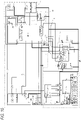
- Fig. 16 is a diagram showing an operation of the electric circuit in the charging mode. In each of Figs.
- the terminals surrounded by dashed ellipse indicate the terminals to and from which the power source voltage V BAT , the USB voltage V USB , the system power source voltage, and the like are input or output.
- the power source voltage V BAT is input to the power source terminal VDD of the protection IC 10, the input terminal VIN of the step-up DC/DC converter 9, and the charging terminal bat of the charging IC 2.
- the MCU 1 enables the V BAT power path function of the charging IC 2, and disables the OTG function and the charging function. Since the USB voltage V USB is not input to the input terminal VBUS of the charging IC 2, the V BAT power path function of the charging IC 2 is effective. Since a signal for enabling the OTG function is not output from the MCU 1 to the charging IC 2 through the communication line LN, the OTG function is disabled. Therefore, the charging IC 2 generates the system power source voltage Vcc0 from the power source voltage V BAT input to the charging terminal bat, and outputs the generated system power source voltage Vcc0 from the output terminal SYS.
- the system power source voltage Vcc0 output from the output terminal SYS is input to the power source terminal VDD of the MCU 1, the power source terminal VDD of the Hall IC 13, the power source terminal VCC of the communication IC 15, and the power source terminal VDD of the Hall IC 14.
- the system power source voltage Vcc0 is set to be lower than the USB voltage V USB input from the external power source to the power source input terminal V USB at the time of charging.
- the MCU 1 activates the OTG function of the charging IC 2 via the communication line LN when the signal input to the terminal P8 is the high level and the MCU 1 detects that the slider 119 is opened from the sleep mode state of Fig. 11 . Accordingly, the charging IC 2 outputs, from the input terminal VBUS, the system power source voltage Vcc4 obtained by stepping up the power source voltage V BAT input from the charging terminal bat. The system power source voltage Vcc4 output from the input terminal VBUS is supplied to the LEDs L1 to L8.
- the MCU 1 When the signal input to the terminal P4 is a low level (the operation switch OPS is pressed) from the state of Fig. 12 , the MCU 1 performs various settings necessary for the heating, and then inputs a high level enable signal from the terminal P14 to the enable terminal EN of the step-up DC/DC converter 9. Accordingly, the step-up DC/DC converter 9 outputs a drive voltage V bst obtained by stepping up the power source voltage V BAT from the output terminal VOUT. The drive voltage V bst is supplied to the switches S3 and S4. In this state, the switches S3 and S4 are turned off. Thereafter, the operation mode is shifted to the heating mode.
- the MCU 1 starts switching control of the switch S3 connected to the terminal P16 and switching control of the switch S4 connected to the terminal P15. These switching controls may be automatically started when the heating initial setting mode described above is completed, or may be started by further pressing the operation switch OPS. Specifically, as shown in Fig. 14 , the MCU 1 performs the heating control of turning on the switch S3, turning off the switch S4, supplying the drive voltage V bst to the heater HTR, and performing the heating of the heater HTR for generating the aerosol, and as shown in Fig. 15 , performs temperature detection control of turning off the switch S3, turning on the switch S4, and detecting the temperature of the heater HTR.
- the drive voltage V bst is input to the positive power source terminal of the operational amplifier OP1 and is also input to the voltage dividing circuit Pb.
- the voltage divided by the voltage dividing circuit Pb is input to the terminal P18 of the MCU 1.
- the MCU 1 acquires the voltage of the positive power source terminal of the operational amplifier OP1 at the time of the temperature detection control based on the voltage input to the terminal P18.
- the drive voltage V bst is supplied to the series circuit of the resistor Rs and the heater HTR. Then, a voltage V heat obtained by dividing the drive voltage V bst by the resistor Rs and the heater HTR is input to the non-inverting input terminal of the operational amplifier OP1.
- the operational amplifier OP1 amplifies and outputs a difference between the voltage input to the inverting input terminal and the voltage V heat input to the non-inverting input terminal.
- the output signal of the operational amplifier OP1 is input to the terminal P9 of the MCU 1.
- the MCU 1 acquires the temperature of the heater HTR based on the signal input to the terminal P9, the voltage of the positive power source terminal of the operational amplifier OP1 acquired based on the input voltage of the terminal P18, and a known electrical resistance value of the resistor Rs.
- Fig. 16 shows a case where the USB connection is made in the sleep mode.
- the USB voltage V USB is input to the input terminal VIN of the LSW 3 via the overvoltage protection IC 11.
- the USB voltage V USB is also supplied to the voltage dividing circuit Pf connected to the input terminal VIN of the LSW 3. Since the bipolar transistor S2 is turned on immediately after the USB connection is made, the signal input to the control terminal ON of the LSW 3 remains at the low level.
- the USB voltage V USB is also supplied to the voltage dividing circuit Pc connected to the terminal P17 of the MCU 1, and the voltage divided by the voltage dividing circuit Pc is input to the terminal P17.
- the MCU 1 detects the USB connection based on the voltage input to the terminal P17.
- the voltage dividing circuit Pc is configured to make the voltage input to the terminal P17 equal to or lower than the system power source voltage Vcc0 input to the power source terminal VDD of the MCU 1.
- the MCU 1 When the MCU 1 detects that the USB connection is made, the MCU 1 turns off the bipolar transistor S2 connected to the terminal P19.
- the USB voltage V USB divided by the voltage dividing circuit Pf is input to the control terminal ON of the LSW 3. Accordingly, the high-level signal is input to the control terminal ON of the LSW 3, and the LSW 3 outputs the USB voltage V USB from the output terminal VOUT.
- the USB voltage V USB output from the LSW 3 is input to the input terminal VBUS of the charging IC 2.
- the USB voltage V USB output from the LSW 3 is supplied as it is to the LEDs L1 to L8 as the system power source voltage Vcc4.
- the MCU 1 When the MCU 1 detects that the USB connection is made, the MCU 1 further outputs a low-level enable signal from the terminal P22 to the charge enable terminal CE (-) of the charging IC 2. Accordingly, the charging IC 2 enables the charging function of the power source BAT, and starts charging the power source BAT with the USB voltage V USB input to the input terminal VBUS. At this time, the MCU 1 does not perform the heating of the heater HTR for generating the aerosol while the switch S3 and the switch S4 are turned off. In other words, when the MCU 1 detects that the USB connection is made based on the voltage input to the terminal P17, the MCU 1 prohibits the supply of power from the power source BAT to the heater connector Cn. Accordingly, it is possible to avoid power consumption from the power source BAT at the time of charging.
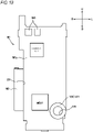
- Fig. 17 is a diagram showing the primary surface 162a of the receptacle-mounted board 162.
- the primary surface 162a of the receptacle-mounted board 162 is a surface on one side of the region SP formed by the two boards 161 and 162 held in parallel.
- the heater connector Cn is disposed in the vicinity of an upper end portion, the receptacle RCP is disposed at a lower end portion, and the reactor Lc of the step-up DC/DC converter 9 is disposed between the heater connector Cn and the receptacle RCP.
- a battery connector 222 on a positive electrode side (hereinafter, referred to as a positive electrode side battery connector 222) is disposed on a right side, and the opening 176 into which the second small diameter portion 192b of the spacer 173 is fitted is disposed on a left side.
- a battery connector 224 on a negative electrode side (hereinafter, referred to as a negative electrode side battery connector 224) and power source temperature detection connectors 234 connected to the thermistor T1 constituting the power source temperature sensor are disposed.
- a positive electrode side power source bus bar 236 (see Figs.
- a negative electrode side power source bus bar 238 (see Figs. 7 and 8 ) extending from the negative electrode terminal of the power source BAT is connected to the negative electrode side battery connector 224.
- the receptacle RCP is disposed at the lower end portion of the receptacle-mounted board 162, and the opening 176 to which the spacer 173 and the receptacle-mounted board 162 are connected is closer to the lower end portion side with respect to the upper end portion. That is, in the receptacle-mounted board 162 extending in the up-down direction, the receptacle RCP and the opening 176 are disposed close to the same side (lower end side in the present embodiment) in the up-down direction.
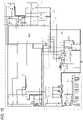
- Fig. 18 is a diagram showing the secondary surface 162b of the receptacle-mounted board 162.
- the overvoltage protection IC 11 is disposed below the opening 176
- the protection IC 10 the operational amplifier OP1, and the step-up DC/DC converter 9 are disposed above the opening 176 in this order from below.
- Fig. 19 is a diagram showing the primary surface 161a of the MCU-mounted board 161.
- heater temperature detection connectors 240 to which the thermistor T3 constituting the heater temperature sensor is connected via a conductive wire are disposed at an upper end portion, and the charging IC 2 is disposed below the heater temperature detection connectors 240.
- the opening 175 into which the first small diameter portion 192a of the spacer 173 is fitted is disposed at a position corresponding to the opening 176 of the receptacle-mounted board 162, and the MCU 1 is disposed in the vicinity of the opening 175.
- the MCU 1 is disposed on the lower side of the MCU-mounted board 161, and the opening 175 to which the spacer 173 and the MCU-mounted board 161 are connected is closer to the lower end portion side with respect to the upper end portion. That is, in the MCU-mounted board 161 extending in the up-down direction, the MCU 1 and the opening 175 are disposed close to the same side (the lower end side in the present embodiment) in the up-down direction.
- the opening peripheral edge portion 166 around the opening 175 of the MCU-mounted board 161 is an insulating portion 167, and a bolt head of the bolt 136 for fixing the MCU-mounted board 161 and the receptacle-mounted board 162 to the chassis 150 comes into contact with the opening peripheral edge portion 166.
- the electrical connection between the head of the bolt 136 and the opening peripheral edge portion 166 of the MCU-mounted board 161 is cut off by the insulating portion 167.
- the MCU 1 By disposing the MCU 1 on the MCU-mounted board 161 with respect to the receptacle-mounted board 162 on which the receptacle RCP is disposed, since the MCU 1 is separated from the receptacle RCP, the MCU 1 is less likely to be affected by static electricity or the like that may enter from the receptacle RCP. Accordingly, the operation of the suction device 100 can be made more stable.
- Fig. 20 is a diagram showing the secondary surface 161b of the MCU-mounted board 161.
- the secondary surface 161b of the MCU-mounted board 161 is a surface on the other side of the region SP formed by the two boards 161 and 162 held in parallel.
- a motor connector 226 to which the vibration motor M is connected via a conductive wire is disposed above the opening 175, and case temperature detection connectors 228 to which the thermistor T4 constituting the case temperature sensor is connected via a conductive wire and intake air detection connectors 230 to which the thermistor T2 constituting the intake sensor is connected via a conductive wire are disposed above the motor connector 226.
- Fig. 21 is a cross-sectional view of the suction device 100.
- a plurality of elements and ICs are mounted on the primary surface 161a and the secondary surface 161b of the MCU-mounted board 161 and the primary surface 162a and the secondary surface 162b of the receptacle-mounted board 162.
- the reactor Lc connected to the receptacle RCP and the step-up DC/DC converter 9 is disposed as described above.
- a reference numeral 300 denotes a heat diffusion member that dissipates heat generated by the step-up DC/DC converter 9 or the like.
- the board area can be effectively utilized. Accordingly, the cost and the size of the suction device 100 can be reduced.
- the size of the reactor Lc connected to the step-up DC/DC converter 9 increases in accordance with the current output from the step-up DC/DC converter 9.
- the reactor Lc is likely to be larger than the step-up DC/DC converter 9 itself.
- the spacer 173 has the cylindrical shape, but the present invention is not limited thereto, and the spacer 173 may have a tubular shape as long as there is the through hole 194 through which the bolt 136 is inserted.
- the power source unit of the aerosol generating device further includes: a chassis (chassis 150) disposed inside the case, in which the first board and the second board are fixed to the chassis.
- the cost of the power source unit of the aerosol generating device can be reduced by using the bolts having high versatility.
- the power supply unit of an aerosol generating device in which an opening peripheral edge portion (opening peripheral edge portion 166) of the first board in contact with a head of the bolt includes an insulating portion (insulating portion 167).
- the electrical connection between the head of the bolt and the opening peripheral edge portion of the first board is cut off by the insulating portion.
- the power supply unit of an aerosol generating device further includes:
- the ground potentials of the two grounds can be equalized, and the supply and communication of the charging power and the operating power between the IC of the first board and the IC of the second board can be stabilized. Further, since the volume of the spacer can be freely set, the resistance can be reduced by increasing the volume of the spacer.
- the power supply unit of an aerosol generating device further includes:
- the board area can be effectively utilized. Accordingly, the cost and the size of the power source unit of the aerosol generating device can be reduced.
- the power supply unit of an aerosol generating device further includes:
- the size of the reactor connected to the voltage conversion IC increases in accordance with the current output from the voltage conversion IC.
- the reactor is likely to be larger than the voltage conversion IC itself. According to (10), by disposing the reactor having a large volume between the first board and the second board, it is possible to prevent the reactor from protruding to the outside.
Landscapes
- Direct Current Feeding And Distribution (AREA)
- Charge And Discharge Circuits For Batteries Or The Like (AREA)
Abstract
Description
- The present invention relates to a power source unit of an aeroslo generating device.
- In a power source unit of an aerosol generating device, a plurality of boards may be disposed in a case.
- For example,
JP-T-2020-531015 - However, when a plurality of boards are arranged adjacent to each other in the case, the boards may come into contact with each other depending on a fixing method thereof or a usage environment of a user, which may cause a short circuit.
- The present invention provides a power source unit of an aerosol generating device capable of appropriately avoiding contact between boards in a case.
- According to an aspect of the present invention, there is provided a power source unit of an aerosol generating device including: a power source; a heater connector to which a heater configured to heat an aerosol source by consuming power supplied from the power source is connected; a first board; a second board separate from the first board; a case in which the power source, the heater connector, the first board, and the second board are housed; and a spacer disposed between the first board and the second board and configured to hold the first board and the second board in parallel.
- According to the aspect of the present invention, it is possible to appropriately avoid contact between the boards in the case.
-
-
Fig. 1 is a perspective view of a non-combustion-type suction device. -
Fig. 2 is a perspective view of the non-combustion-type suction device with a rod attached. -
Fig. 3 is another perspective view of the non-combustion-type suction device. -
Fig. 4 is an exploded perspective view of the non-combustion-type suction device. -
Fig. 5 is a perspective view of an internal unit of the non-combustion-type suction device. -
Fig. 6 is an exploded perspective view of the internal unit ofFig. 5 . -
Fig. 7 is a perspective view of the internal unit from which a power source and a chassis are removed. -
Fig. 8 is another perspective view of the internal unit from which the power source and the chassis are removed. -
Fig. 9 is a schematic diagram showing operation modes of the suction device. -
Fig. 10 is a diagram showing a schematic configuration of an electric circuit of the internal unit. -
Fig. 11 is a diagram showing an operation of the electric circuit in a sleep mode. -
Fig. 12 is a diagram showing an operation of the electric circuit in an active mode. -
Fig. 13 is a diagram showing an operation of the electric circuit in a heating initial setting mode. -
Fig. 14 is a diagram showing an operation of the electric circuit at a time of heating of a heater in a heating mode. -
Fig. 15 is a diagram showing an operation of the electric circuit at a time of detecting a temperature of the heater in the heating mode. -
Fig. 16 is a diagram showing an operation of the electric circuit in a charging mode. -
Fig. 17 is a view showing a primary surface of a receptacle-mounted board. -
Fig. 18 is a view showing a secondary surface of the receptacle-mounted board. -
Fig. 19 is a view showing a primary surface of an MCU-mounted board. -
Fig. 20 is a view showing a secondary surface of the MCU-mounted board. -
Fig. 21 is a cross-sectional view of the non-combustion-type suction device. -
Fig. 22 is a perspective view of a spacer. - Hereinafter, a suction system according to an embodiment of an aerosol generating device in the present invention will be described with reference to the drawings. The suction system includes a non-combustion-type suction device 100 (hereinafter, also simply referred to as the "
suction device 100") that is an embodiment of a power source unit of the present invention, and arod 500 heated by thesuction device 100. In the following description, a configuration in which thesuction device 100 undetachably houses a heating unit will be described as an example. However, the heating unit may be configured to be detachable from thesuction device 100. For example, a unit in which therod 500 and the heating unit are integrated may be configured to be detachable from thesuction device 100. That is, the power source unit of an aerosol generating device may not include the heating unit as a constituent element. The term "undetachable" refers to a mode in which detachment cannot be performed as long as intended use is intended. Alternatively, the heating unit may be configured by cooperation of an induction heating coil provided in thesuction device 100 and a susceptor incorporated in therod 500. -
Fig. 1 is a perspective view showing an overall configuration of thesuction device 100.Fig. 2 is a perspective view of thesuction device 100 with therod 500 attached.Fig. 3 is another perspective view of thesuction device 100.Fig. 4 is an exploded perspective view of thesuction device 100. In the following description, a three-dimensional space orthogonal coordinate system is described in which three directions orthogonal to each other are referred to as a front-rear direction, a left-right direction, and an up-down direction for the sake of convenience. In the drawings, Fr denotes a front side, Rr denotes a rear side, R denotes a right side, L denotes a left side, U denotes an upper side, and D denotes a lower side. - The
suction device 100 is configured to generate aerosol containing flavor by heating the elongated, substantially cylindrical rod 500 (seeFig. 2 ) serving as an example of a flavor component generating base material having a filler containing an aerosol source, a flavor source, and the like. - The
rod 500 contains the filler containing the aerosol source that is heated at a predetermined temperature to generate the aerosol. - A type of the aerosol source is not particularly limited, and extraction substances from various natural products and/or constituent components thereof can be selected according to an intended use. The aerosol source may be a solid, or may be, for example, a polyhydric alcohol such as glycerin or propylene glycol, or a liquid such as water. The aerosol source may contain the flavor source such as a cigarette raw material that releases a flavor component by heating or an extract derived from the cigarette raw material. Gas to which the flavor component is added is not limited to the aerosol, and for example, invisible steam may be generated.
- The filler of the
rod 500 may contain cigarettes as the flavor source. A material of the cigarettes is not particularly limited, and known materials such as lamina and midbone can be used. The filler may contain one kind or two or more kinds of fragrances. A type of the fragrance is not particularly limited, and is preferably menthole from a viewpoint of imparting a good draft. The flavor source may contain a plant (for example, mint, Kampo, or herb) other than a cigarette. Depending on applications, therod 500 may not include the flavor source. - Next, the overall configuration of the
suction device 100 will be described with reference toFigs. 1 to 4 . Thesuction device 100 includes a substantially rectangularparallelepiped case 110 having a front surface, a rear surface, a left surface, a right surface, an upper surface, and a lower surface. Thecase 110 includes a bottomed cylindrical casemain body 112 in which the front surface, the rear surface, the upper surface, the lower surface, and the right surface are integrally formed, anouter panel 115 and aninner panel 118 that seal an opening 114 (seeFig. 4 ) of the casemain body 112 and form the left surface, and aslider 119. - The
inner panel 118 is fixed to the casemain body 112 by abolt 120. Theouter panel 115 is fixed to the casemain body 112 so as to cover an outer surface of theinner panel 118 bymagnets 124 held by a chassis 150 (seeFig. 5 ), which will be described later, housed in the casemain body 112. Since theouter panel 115 is fixed by themagnets 124, a user can replace theouter panel 115 in accordance with his or her preference. - The
inner panel 118 is provided with two throughholes 126 through which themagnets 124 penetrate. In theinner panel 118, a verticallylong hole 127 and a circularround hole 128 are further provided between the two throughholes 126 disposed in the up-down direction. Thelong hole 127 is for transmitting light emitted from eight light emitting diodes (LEDs) L1 to L8 incorporated in the casemain body 112. A button-type operation switch OPS incorporated in the casemain body 112 passes through theround hole 128. Accordingly, the user can detect the light emitted from the eight LEDs L1 to L8 via anLED window 116 of theouter panel 115. Further, the user can press down the operation switch OPS via apressing portion 117 of theouter panel 115. - As shown in
Fig. 2 , anopening 132 into which therod 500 can be inserted is provided in the upper surface of the casemain body 112. Theslider 119 is coupled to the casemain body 112 so as to be movable in the front-rear direction between a position (seeFig. 1 ) where theopening 132 is closed and a position (seeFig. 2 ) where theopening 132 is opened. InFig. 2 , it should be noted that theslider 119 is transparent and only an outer shape of theslider 119 is indicated by a two-dot chain line in order to facilitate understanding. - The operation switch OPS is used to perform various operations of the
suction device 100. For example, the user operates the operation switch OPS via thepressing portion 117 in a state in which therod 500 is inserted into and attached to theopening 132 as shown inFig. 2 . Accordingly, therod 500 is heated by a heating unit 170 (seeFig. 5 ) without being burned. When therod 500 is heated, the aerosol is generated from the aerosol source contained in therod 500, and the flavor of the flavor source contained in therod 500 is added to the aerosol. The user can suction the aerosol containing the flavor by holding asuction port 502 of therod 500 protruding from theopening 132 in mouth and suctioning. - As shown in
Fig. 3 , a chargingterminal 134 that is electrically connected to an external power source such as an outlet or a mobile battery to receive power supply is provided in the lower surface of the casemain body 112. In the present embodiment, the chargingterminal 134 is a universal serial bus (USB) Type-C receptacle, and is not limited thereto. The chargingterminal 134 is hereinafter also referred to as a receptacle RCP. - The charging
terminal 134 may include, for example, a power receiving coil, and may be configured to receive electric power transmitted from the external power source in a non-contact manner. In this case, a power transmission (wireless power transfer) method may be an electromagnetic induction type, a magnetic resonance type, or a combination of the electromagnetic induction type and the magnetic resonance type. As another example, the chargingterminal 134 can be connected to various USB terminals or the like, and may include the power receiving coil described above. - The configuration of the
suction device 100 shown inFigs. 1 to 4 is merely an example. Thesuction device 100 can be configured in various forms such that the gas to which the flavor component is imparted is generated from therod 500 by holding therod 500 and applying an action such as heating, and the user can suction the generated gas. - An
internal unit 140 of thesuction device 100 will be described with reference toFigs. 5 to 8 .Fig. 5 is a perspective view of theinternal unit 140 of thesuction device 100.Fig. 6 is an exploded perspective view of theinternal unit 140 ofFig. 5 .Fig. 7 is a perspective view of theinternal unit 140 from which a power source BAT and thechassis 150 are removed.Fig. 8 is another perspective view of theinternal unit 140 from which the power source BAT and thechassis 150 are removed. - The
internal unit 140 housed in an internal space of thecase 110 includes thechassis 150, the power source BAT, acircuit unit 160, theheating unit 170, anotification unit 180, and various sensors. - The
chassis 150 includes a plate-shaped chassismain body 151 that is disposed substantially at a center of the internal space of thecase 110 in the front-rear direction and extends in the up-down direction and the front-rear direction, a plate-shaped front-rear dividing wall 152 that is disposed substantially at the center of the internal space of thecase 110 in the front-rear direction and extends in the up-down direction and the left-right direction, a plate-shaped up-downdividing wall 153 that extends forward from substantially a center of the front-rear dividing wall 152 in the up-down direction, a plate-shaped chassisupper wall 154 that extends rearward from upper edge portions of the front-rear dividing wall 152 and the chassismain body 151, and a plate-shaped chassislower wall 155 that extends rearward from lower edge portions of the front-rear dividing wall 152 and the chassismain body 151. A left surface of the chassismain body 151 is covered with theinner panel 118 and theouter panel 115 of thecase 110 described above. - In the internal space of the
case 110, a heatingunit housing region 142 is defined and formed in an upper front portion by thechassis 150, aboard housing region 144 is defined and formed in a lower front portion, and a powersource housing space 146 is defined and formed in a rear portion along the up-down direction. - The
heating unit 170 housed in the heatingunit housing region 142 is constituted by a plurality of cylindrical members, and the plurality of cylindrical members are concentrically arranged to form a cylindrical body as a whole. Theheating unit 170 includes arod housing portion 172 capable of housing a part of therod 500 therein, and a heater HTR (seeFigs. 10 to 16 ) that heats therod 500 from an outer periphery or a center of therod 500. It is preferable that a surface of therod housing portion 172 and the heater HTR are insulated from each other by forming therod housing portion 172 with a heat insulating material or providing the heat insulating material inside therod housing portion 172. It is sufficient that the heater HTR is an element capable of heating therod 500. The heater HTR is, for example, a heating element. Examples of the heating element include a heating resistor, a ceramic heater, and an induction heating type heater. As the heater HTR, for example, a heater having a positive temperature coefficient (PTC) characteristic in which a resistance value increases with an increase in temperature is preferably used. Alternatively, the heater HTR having a negative temperature coefficient (NTC) characteristic in which the resistance value decreases with the increase in temperature may be used. Theheating unit 170 has a function of defining a flow path of air to be supplied to therod 500 and a function of heating therod 500. Thecase 110 is formed with a vent (not shown) through which the air flows in, and is configured such that the air can flow into theheating unit 170. - The power source BAT housed in the power
source housing space 146 is a rechargeable secondary battery, an electric double layer capacitor, or the like, and is preferably a lithium ion secondary battery. An electrolyte of the power source BAT may one or a combination of a gel electrolyte, an electrolytic solution, a solid electrolyte, and an ionic liquid. - The
notification unit 180 notifies various kinds of information such as a state of charge (SOC) indicating a charging state of the power source BAT, a preheating time at a time of suction, and a suction possible period. Thenotification unit 180 according to the present embodiment includes the eight LEDs L1 to L8 and a vibration motor M. Thenotification unit 180 may include a light emitting element such as the LEDs L1 to L8, may include a vibration element such as the vibration motor M, or may include a sound output element. Thenotification unit 180 may be a combination of two or more of the light emitting element, the vibration element, and the sound output element. - The various sensors include an intake sensor that detects a puff operation (suction operation) of the user, a power source temperature sensor that detects a temperature of the power source BAT, a heater temperature sensor that detects a temperature of the heater HTR, a case temperature sensor that detects a temperature of the
case 110, a cover position sensor that detects a position of theslider 119, a panel detection sensor that detects attachment and detachment of theouter panel 115, and the like. - The intake sensor mainly includes, for example, a thermistor T2 disposed in the vicinity of the
opening 132. The power source temperature sensor mainly includes, for example, a thermistor T1 disposed in the vicinity of the power source BAT. The heater temperature sensor mainly includes, for example, a thermistor T3 disposed in the vicinity of the heater HTR. As described above, therod housing portion 172 is preferably insulated from the heater HTR. In this case, the thermistor T3 is preferably in contact with or close to the heater HTR inside therod housing portion 172. When the heater HTR has the PTC characteristic or the NTC characteristic, the heater HTR itself may be used as the heater temperature sensor. The case temperature sensor mainly includes, for example, a thermistor T4 disposed in the vicinity of the left surface of thecase 110. The cover position sensor mainly includes a Hall IC 14 (seeFigs. 10 to 16 ) including a Hall element disposed in the vicinity of theslider 119. The panel detection sensor mainly includes a Hall IC 13 (seeFigs. 10 to 16 ) including a Hall element disposed in the vicinity of an inner surface of theinner panel 118. - The
circuit unit 160 includes four circuit boards, a plurality of integrate circuits (ICs), and a plurality of elements. The four circuit boards include an MCU-mountedboard 161 on which a micro controller unit (MCU) 1 and a chargingIC 2 to be described later are mainly disposed, a receptacle-mountedboard 162 on which the chargingterminal 134 is mainly disposed, an LED-mountedboard 163 on which the operation switch OPS, the LEDs L1 to L8, and acommunication IC 15 to be described later are disposed, and a Hall IC-mountedboard 164 on which theHall IC 14 to be described later including the Hall element constituting the cover position sensor is disposed. - The MCU-mounted
board 161 and the receptacle-mountedboard 162 are arranged parallel to each other in theboard housing region 144. Specifically, the MCU-mountedboard 161 and the receptacle-mountedboard 162 are arranged such that respective element arrangement surfaces thereof are arranged along the left-right direction and the up-down direction, and the MCU-mountedboard 161 is arranged in front of the receptacle-mountedboard 162. The MCU-mountedboard 161 and the receptacle-mountedboard 162 are provided withopenings 175 and 176 (seeFigs. 17 to 20 ), respectively. The MCU-mountedboard 161 and the receptacle-mountedboard 162 are fixed to thechassis 150 with abolt 136 in a state in which aspacer 173 is interposed between openingperipheral edge portions portions -
Fig. 22 is a perspective view of thespacer 173. - As shown in
Fig. 22 , thespacer 173 includes alarge diameter portion 191, a firstsmall diameter portion 192a that is provided on one end side of thelarge diameter portion 191 and has a smaller diameter than that of thelarge diameter portion 191, a secondsmall diameter portion 192b that is provided on the other end side of thelarge diameter portion 191 and has a smaller diameter than that of thelarge diameter portion 191, afirst disk portion 193a that connects one end of thelarge diameter portion 191 and the firstsmall diameter portion 192a, asecond disk portion 193b that connects the other end of thelarge diameter portion 191 and the secondsmall diameter portion 192b, and a throughhole 194 that is formed across the firstsmall diameter portion 192a, thelarge diameter portion 191, and the secondsmall diameter portion 192b, and has a cylindrical shape as a whole. Thefirst disk portion 193a and thesecond disk portion 193b are formed parallel to each other. - The
bolt 136 is inserted through theopening 175 of the MCU-mountedboard 161, the throughhole 194 of thecylindrical spacer 173, and theopening 176 of the receptacle-mountedboard 162, and is fixed to aboard fixing portion 156 of the front-rear dividing wall 152 disposed between the MCU-mountedboard 161 and the receptacle-mountedboard 162 and the power source BAT in the front-rear direction with thespacer 173 interposed therebetween. At this time, the firstsmall diameter portion 192a is fitted into and connected to theopening 175 of the MCU-mountedboard 161, and the secondsmall diameter portion 192b is fitted into and connected to theopening 176 of the receptacle-mountedboard 162. Meanwhile, thefirst disk portion 193a comes into contact with the opening peripheral edge portion 166 (seeFig. 20 ) of asecondary surface 161b of the MCU-mountedboard 161, and thesecond disk portion 193b comes into contact with the opening peripheral edge portion 168 (seeFig. 17 ) of aprimary surface 162a of the receptacle-mountedboard 162. Accordingly, the MCU-mountedboard 161 and the receptacle-mountedboard 162 are held in parallel by thespacer 173. - That is, the
spacer 173 is a holding member that is disposed between the MCU-mountedboard 161 and the receptacle-mountedboard 162 and holds the MCU-mountedboard 161 and the receptacle-mountedboard 162 in parallel. In this way, by holding the twoboards case 110 in parallel via thespacer 173, it is possible to prevent theboards boards case 110, and the internal space of thecase 110 can be effectively used. A width (a length in the front-rear direction) of the region SP is equal to a length of thelarge diameter portion 191 of thespacer 173. By fixing the MCU-mountedboard 161 and the receptacle-mountedboard 162 to thechassis 150 in thecase 110, the twoboards rear dividing wall 152 of thechassis 150 is disposed between the MCU-mountedboard 161 and the receptacle-mountedboard 162 and the power source BAT, the power source BAT and the twoboards boards - The
spacer 173 has conductivity, and grounds of the MCU-mountedboard 161 and the receptacle-mountedboard 162 are connected via thespacer 173. More specifically, the firstsmall diameter portion 192a fitted into theopening 175 of the MCU-mountedboard 161 is connected to the ground inside the MCU-mountedboard 161, and the secondsmall diameter portion 192b fitted into theopening 176 of the receptacle-mountedboard 162 is connected to the ground inside the receptacle-mountedboard 162. Accordingly, ground potentials of the MCU-mountedboard 161 and the receptacle-mountedboard 162 can be equalized, and supply of charging power and operating power and communication between the MCU-mountedboard 161 and the receptacle-mountedboard 162 can be stabilized. Further, since a volume of thespacer 173 can be freely set, a resistance can be reduced by making thespacer 173 thick and short. - For the sake of convenience, when surfaces of the MCU-mounted
board 161 and the receptacle-mountedboard 162 facing forward are defined asprimary surfaces primary surfaces secondary surfaces secondary surface 161b of the MCU-mountedboard 161 and theprimary surface 162a of the receptacle-mountedboard 162 face each other with a predetermined gap therebetween, thereby forming the electrically safe region SP described above. Theprimary surface 161a of the MCU-mountedboard 161 faces the front surface of thecase 110, and thesecondary surface 162b of the receptacle-mountedboard 162 faces the front-rear dividing wall 152 of thechassis 150. - The MCU-mounted
board 161 and the receptacle-mountedboard 162 are electrically connected to each other via aflexible wiring board 165. Theflexible wiring board 165 that electrically connects the MCU-mountedboard 161 and the receptacle-mountedboard 162 connectsFPC connection portions board 161 and the receptacle-mountedboard 162 to each other (seeFigs. 17 to 20 ). Elements and ICs mounted on the MCU-mountedboard 161 and the receptacle-mountedboard 162 will be described later. - The LED-mounted
board 163 is disposed on a left side surface of the chassismain body 151 and between the twomagnets 124 disposed in the up-down direction. An element arrangement surface of the LED-mountedboard 163 is disposed along the up-down direction and the front-rear direction. In other words, the element arrangement surface of each of the MCU-mountedboard 161 and the receptacle-mountedboard 162 is orthogonal to the element arrangement surface of the LED-mountedboard 163. In this way, the element arrangement surface of each of the MCU-mountedboard 161 and the receptacle-mountedboard 162 and the element arrangement surface of the LED-mountedboard 163 are not limited to be orthogonal to each other, and preferably intersect with each other (are not parallel to each other). The vibration motor M constituting thenotification unit 180 together with the LEDs L1 to L8 is fixed to a lower surface of the chassislower wall 155 and is electrically connected to the MCU-mountedboard 161. - The Hall IC-mounted
board 164 is disposed on an upper surface of the chassisupper wall 154. -
Fig. 9 is a schematic diagram showing operation modes of thesuction device 100. As shown inFig. 9 , the operation modes of thesuction device 100 include a charging mode, a sleep mode, an active mode, a heating initial setting mode, a heating mode, and a heating completion mode. - The sleep mode is a mode in which power saving is achieved by mainly stopping power supply to electrical components necessary for heating control of the heater HTR.
- The active mode is a mode in which most of functions other than heating control of the heater HTR are enabled. When the
slider 119 is opened while thesuction device 100 is operating in the sleep mode, thesuction device 100 switches the operation mode to the active mode. When theslider 119 is closed or a non-operation time of the operation switch OPS reaches a predetermined time while thesuction device 100 is operating in the active mode, thesuction device 100 switches the operation mode to the sleep mode. - The heating initial setting mode is a mode in which an initial setting of control parameters and the like for starting heating control of the heater HTR is performed. When the
suction device 100 detects an operation of the operation switch OPS while operating in the active mode, thesuction device 100 switches the operation mode to the heating initial setting mode, and when the initial setting is finished, thesuction device 100 switches the operation mode to the heating mode. - The heating mode is a mode in which the heating control (heating control for aerosol generation and heating control for temperature detection) of the heater HTR is executed. When the operation mode is switched to the heating mode, the
suction device 100 starts the heating control of the heater HTR. - The heating completion mode is a mode in which processing (processing of storing a heating history or the like) of completing the heating control of the heater HTR is executed. When an energization time of the heater HTR or the number of times user suctions reaches an upper limit or the
slider 119 is closed while thesuction device 100 is operating in the heating mode, thesuction device 100 switches the operation mode to the heating completion mode, and when the completion processing is completed, thesuction device 100 switches the operation mode to the active mode. Thesuction device 100 switches the operation mode to the heating completion mode when a USB connection is made while operating in the heating mode, and when the completion processing is completed, switches the operation mode to the charging mode. As shown inFig. 9 , in this case, the operation mode may be switched to the active mode before the operation mode is switched to the charging mode. In other words, when the USB connection is made while thesuction device 100 is operating in the heating mode, thesuction device 100 may switch the operation mode in an order of the heating completion mode, the active mode, and the charging mode. - The charging mode is a mode in which the power source BAT is charged with power supplied from the external power source connected to the receptacle RCP. When the external power source is connected (USB-connected) to the receptacle RCP while the
suction device 100 is operating in the sleep mode or the active mode, thesuction device 100 switches the operation mode to the charging mode. When the charging of the power source BAT is completed or the connection between the receptacle RCP and the external power source is released while thesuction device 100 is operating in the charging mode, thesuction device 100 switches the operation mode to the sleep mode. -
Fig. 10 is a diagram showing a schematic configuration of an electric circuit of theinternal unit 140.Fig. 10 only shows main elements and ICs. - A wire indicated by a thick solid line in
Fig. 10 is a wire (a wire connected to a ground provided in the internal unit 140) having the same potential as a reference potential (ground potential) of theinternal unit 140, and this wire is hereinafter referred to as a ground line. InFig. 10 , electrical components obtained by chipping a plurality of circuit elements are indicated by rectangles, and reference numerals of various terminals are described inside the rectangles. A power source terminal VCC and a power source terminal VDD mounted on the chip indicate power source terminals on a high potential side, respectively. A power source terminal VSS and a ground terminal GND mounted on the chip are power source terminals on a low potential side (reference potential side), respectively. In the chipped electrical component, a difference between a potential of the power source terminal on the high potential side and a potential of the power source terminal on the low potential side is a power source voltage. The chipped electrical component executes various functions using the power source voltage. - The MCU-mounted
board 161 is provided with, as main electric components, anMCU 1 that performs overall control of theentire suction device 100, the chargingIC 2 that performs charging control of the power source BAT, a load switch (hereinafter, LSW) 3 configured by combining a capacitor, a resistor, a transistor, and the like, and a voltage dividing circuit Pc for USB connection detection. - The ground terminal GND of each of the charging
IC 2 and theLSW 3 is connected to the ground line. - The LED-mounted
board 163 is provided with, as main electric components, theHall IC 13 including a Hall element constituting the panel detection sensor, the LEDs L1 to L8, the operation switch OPS, and thecommunication IC 15. Thecommunication IC 15 is a communication module for communicating with an electronic device such as a smartphone. Each of the power source terminal VSS of theHall IC 13 and the ground terminal GND of thecommunication IC 15 is connected to the ground line. Thecommunication IC 15 and theMCU 1 can communicate with each other through a communication line LN. One end of the operation switch OPS is connected to the ground line, and the other end of the operation switch OPS is connected to a terminal P4 of theMCU 1. - The receptacle-mounted
board 162 is provided with, as main electric components, a power source connector (in the drawing, the power source BAT connected to the power source connector is described) electrically connected to the power source BAT, a step-up DC/DC converter 9 (in the drawing, the step-up DC/DC 9 is described), aprotection IC 10, anovervoltage protection IC 11, the receptacle RCP, switches S3 and S4 constituted by MOSFETs, an operational amplifier OP1, and a pair of (positive electrode side and negative electrode side) heater connectors Cn electrically connected to the heater HTR. - The two ground terminals GND of the receptacle RCP, the ground terminal GND of the step-up DC/
DC converter 9, the power source terminal VSS of theprotection IC 10, the ground terminal GND of theovervoltage protection IC 11, and a negative power source terminal of the operational amplifier OP1 are each connected to the ground line. - The
Hall IC 14 including the Hall element constituting the cover position sensor is provided on the Hall IC-mountedboard 164. The power source terminal VSS of theHall IC 14 is connected to the ground line. An output terminal OUT of theHall IC 14 is connected to a terminal P8 of theMCU 1. TheMCU 1 detects opening and closing of theslider 119 based on a signal input to the terminal P8. - Hereinafter, a connection relationship and the like of each of the electrical components will be described with reference to
Fig. 10 . - Two power input terminals VBUS of the receptacle RCP are connected to an input terminal IN of the
overvoltage protection IC 11 via a protection element such as a fuse Fs. When a USB plug is connected to the receptacle RCP and a USB cable including the USB plug is connected to the external power source, a USB voltage VUSB is supplied to two power input terminals VBUS of the receptacle RCP. - The input terminal IN of the
overvoltage protection IC 11 is connected to one end of a voltage dividing circuit Pa including a series circuit of two resistors. The other end of the voltage dividing circuit Pa is connected to the ground line. A connection point of the two resistors constituting the voltage dividing circuit Pa is connected to a voltage detection terminal OVLo of theovervoltage protection IC 11. When a voltage input to the voltage detection terminal OVLo is less than a threshold, theovervoltage protection IC 11 outputs a voltage input to the input terminal IN from the output terminal OUT. When the voltage input to the voltage detection terminal OVLo is equal to or higher than a threshold (overvoltage), theovervoltage protection IC 11 stops the voltage output from the output terminal OUT (cuts off the electrical connection between theLSW 3 and the receptacle RCP), thereby protecting the electrical components downstream of theovervoltage protection IC 11. The output terminal OUT of theovervoltage protection IC 11 is connected to an input terminal VIN of theLSW 3 and one end of the voltage dividing circuit Pc (the series circuit of two resistors) connected to theMCU 1. The other end of the voltage dividing circuit Pc is connected to the ground line. A connection point of the two resistors constituting the voltage dividing circuit Pc is connected to a terminal P17 of theMCU 1. - One end of a voltage dividing circuit Pf including a series circuit of two resistors is connected to the input terminal VIN of the
LSW 3. The other end of the voltage dividing circuit Pf is connected to the ground line. A connection point of the two resistors constituting the voltage dividing circuit Pf is connected to a control terminal ON of theLSW 3. A collector terminal of a bipolar transistor S2 is connected to the control terminal ON of theLSW 3. An emitter terminal of the bipolar transistor S2 is connected to the ground line. A base terminal of the bipolar transistor S2 is connected to a terminal P19 of theMCU 1. When a signal input to the control terminal ON is a high level, theLSW 3 outputs a voltage input to the input terminal VIN from an output terminal VOUT. The output terminal VOUT of theLSW 3 is connected to an input terminal VBUS of the chargingIC 2 and an anode of each of the LEDs L1 to L8. - The
MCU 1 turns on the bipolar transistor S2 while the USB connection is not made. Accordingly, since the control terminal ON of theLSW 3 is connected to the ground line via the bipolar transistor S2, a low-level signal is input to the control terminal ON of theLSW 3. - The bipolar transistor S2 connected to the
LSW 3 is turned off by theMCU 1 when the USB connection is made. When the bipolar transistor S2 is turned off, the USB voltage VUSB divided by the voltage dividing circuit Pf is input to the control terminal ON of theLSW 3. Therefore, when the USB connection is made and the bipolar transistor S2 is turned off, a high-level signal is input to the control terminal ON of theLSW 3. Accordingly, theLSW 3 outputs the USB voltage VUSB supplied from the USB cable from the output terminal VOUT. It should be noted that even when the USB connection is made in a state in which the bipolar transistor S2 is not turned off, since the control terminal ON of theLSW 3 is connected to the ground line via the bipolar transistor S2, the low-level signal continues to be input to the control terminal ON of theLSW 3 unless theMCU 1 turns off the bipolar transistor S2. - A positive electrode terminal of the power source BAT is connected to the power source terminal VDD of the
protection IC 10, the input terminal VIN of the step-up DC/DC converter 9, and a charging terminal bat of the chargingIC 2. Therefore, a power source voltage VBAT of the power source BAT is supplied to theprotection IC 10, the chargingIC 2, and the step-up DC/DC converter 9. A resistor Ra, a switch Sa constituted by an MOSFET, and a switch Sb constituted by an MOSFET are connected in series in this order to a negative electrode terminal of the power source BAT. A current detection terminal CS of theprotection IC 10 is connected to a connection point between the resistor Ra and the switch Sa. A control terminal of each of the switches Sa and Sb is connected to theprotection IC 10. - The
protection IC 10 acquires a value of a current flowing through the resistor Ra at a time of charging and discharging of the power source BAT from a voltage input to the current detection terminal CS, and when the current value is excessive (in a case of an overcurrent), theprotection IC 10 performs opening and closing control of the switch Sa and the switch Sb to stop charging or discharging of the power source BAT, thereby protecting the power source BAT. More specifically, when theprotection IC 10 acquires the excessive current value at the time of charging the power source BAT, theprotection IC 10 stops the charging of the power source BAT by turning off the switch Sb. When theprotection IC 10 acquires the excessive current value at the time of discharging the power source BAT, theprotection IC 10 stops the discharging of the power source BAT by turning off the switch Sa. Further, when a voltage value of the power source BAT is abnormal (in a case of overcharge or overvoltage) from the voltage input to the power source terminal VDD, theprotection IC 10 performs opening and closing control of the switch Sa and the switch Sb to stop charging or discharging of the power source BAT, thereby protecting the power source BAT. More specifically, when theprotection IC 10 detects the overcharge of the power source BAT, theprotection IC 10 stops the charging of the power source BAT by turning off the switch Sb. When theprotection IC 10 detects the overdischarge of the power source BAT, theprotection IC 10 stops the discharge of the power source BAT by turning off the switch Sa. - One end of a reactor Lc is connected to a switching terminal SW of the step-up DC/
DC converter 9. The other end of the reactor Lc is connected to the input terminal VIN of the step-up DC/DC converter 9. The step-up DC/DC converter 9 steps up the input voltage by performing on and off control of a built-in transistor connected to the switching terminal SW, and outputs the stepped-up voltage from the output terminal VOUT. The input terminal VIN of the step-up DC/DC converter 9 constitutes a power source terminal on a high potential side of the step-up DC/DC converter 9. The step-up DC/DC converter 9 performs a step-up operation when a signal input to an enable terminal EN is at a high level. In the USB-connected state, the signal input to the enable terminal EN of the step-up DC/DC converter 9 may be controlled to a low level by theMCU 1. Alternatively, in the USB-connected state, theMCU 1 may not control the signal input to the enable terminal EN of the step-up DC/DC converter 9, thereby making a potential of the enable terminal EN indefinite. - The output terminal VOUT of the step-up DC/
DC converter 9 is connected to a source terminal of a switch S4 constituted by a P-channel MOSFET. A gate terminal of the switch S4 is connected to a terminal P15 of theMCU 1. One end of a resistor Rs is connected to a drain terminal of the switch S4. The other end of the resistor Rs is connected to the heater connector Cn on a positive electrode side connected to one end of the heater HTR. A voltage dividing circuit Pb including two resistors is connected to a connection point of the switch S4 and the resistor Rs. A connection point of the two resistors constituting the voltage dividing circuit Pb is connected to a terminal P18 of theMCU 1. The connection point of the switch S4 and the resistor Rs is further connected to a positive power source terminal of the operational amplifier OP1. - A connection line of the output terminal VOUT of the step-up DC/
DC converter 9 and the source terminal of the switch S4 is connected to a source terminal of the switch S3 constituted by a P-channel MOSFET. A gate terminal of the switch S3 is connected to a terminal P16 of theMCU 1. A drain terminal of the switch S3 is connected to a connection line of the resistor Rs and the heater connector Cn on the positive electrode side. In this way, a circuit including the switch S3 and a circuit including the switch S4 and the resistor Rs are connected in parallel between the output terminal VOUT of the step-up DC/DC converter 9 and the positive electrode side of the heater connector Cn. Since the circuit including the switch S3 does not include a resistor, the circuit including the switch S3 has a lower resistance than that of the circuit including the switch S4 and the resistor Rs. - The enable terminal EN of the step-up DC/
DC converter 9 is connected to a terminal P14 of theMCU 1. - A non-inverting input terminal of the operational amplifier OP1 is connected to the connection line of the resistor Rs and the heater connector Cn on the positive electrode side. An inverting input terminal of the operational amplifier OP1 is connected to the heater connector Cn on a negative electrode side connected to the other end of the heater HTR and the ground line. One end of a resistor R4 is connected to an output terminal of the operational amplifier OP1. The other end of the resistor R4 is connected to a terminal P9 of the
MCU 1. - The input terminal VBUS of the charging
IC 2 is connected to the anode of each of the LEDs L1 to L8. Cathodes of the LEDs L1 to L8 are connected to the control terminals PD1 to PD8 of theMCU 1 via resistors for current limitation. That is, the LEDs L1 to L8 are connected in parallel to the input terminal VBUS. The LEDs L1 to L8 are configured to be operable by the USB voltage VUSB supplied from the USB cable connected to the receptacle RCP and the voltage supplied from the power source BAT via the chargingIC 2. Transistors (switching elements) connected to the control terminals PD1 to PD8 and the ground terminal GND are incorporated in theMCU 1. TheMCU 1 turns on the transistor connected to the control terminal PD1 to energize and turn on the LED L1, and turns off the transistor connected to the control terminal PD1 to turn off the LED L1. By switching on and off of the transistor connected to the control terminal PD1 at a high speed, a luminance and a light emission pattern of the LED L1 can be dynamically controlled. The LEDs L2 to L8 are similarly controlled to be turned on by theMCU 1. - The charging
IC 2 has a charging function of charging the power source BAT based on the USB voltage VUSB input to the input terminal VBUS. The chargingIC 2 acquires a charging current or a charging voltage of the power source BAT from a terminal or a wiring (not shown), and performs the charging control of the power source BAT (power supply control from the charging terminal bat to the power source BAT) based on the acquired charging current or the charging voltage. - The charging
IC 2 further includes a VBAT power path function and an OTG function. The VBAT power path function is a function of outputting, from an output terminal SYS, a system power source voltage Vcc0 that is substantially the same as the power source voltage VBAT input to the charging terminal bat. The OTG function is a function of outputting, from the input terminal VBUS, a system power source voltage Vcc4 obtained by stepping up the power source voltage VBAT input to the charging terminal bat. ON/OFF of the OTG function of the chargingIC 2 is controlled by theMCU 1 through serial communication using the communication line LN. In the OTG function, the power source voltage VBAT input to the charging terminal bat may be output from the input terminal VBUS as it is. In this case, the power source voltage VBAT and the system power source voltage Vcc4 are substantially the same. It should be noted that in order to perform the serial communication, a plurality of signal lines such as a data line for data transmission and a clock line for synchronization are required, and only one signal line is shown inFigs. 10 to 16 for simplification. - The output terminal SYS of the charging
IC 2 is connected to the power source terminal VDD of theMCU 1, the power source terminal VDD of theHall IC 13, the power source terminal VCC of thecommunication IC 15, the power source terminal VDD of theHall IC 14, and a series circuit (a series circuit of a resistor and a capacitor) connected to the operation switch OPS. A charge enable terminal CE (-) of the chargingIC 2 is connected to a terminal P22 of theMCU 1 via a resistor. In order to stabilize the voltage supplied to these power source terminals, a voltage regulator may be connected to the output terminal SYS of the chargingIC 2. - The output terminal OUT of the
Hall IC 13 is connected to a terminal P3 of theMCU 1. When theouter panel 115 is detached, a low-level signal is output from the output terminal OUT of theHall IC 13. TheMCU 1 determines whether theouter panel 115 is attached based on the signal input to the terminal P3. - The LED-mounted
board 163 is provided with a series circuit (a series circuit of a resistor and a capacitor) connected to the operation switch OPS. The series circuit is connected to a power source line that connects the output terminal SYS of the chargingIC 2 to the power source terminal VDD of theMCU 1, the power source terminal VDD of theHall IC 13, the power source terminal VDD of theHall IC 14, and the power source terminal VCC of thecommunication IC 15. A connection point of the resistor and the capacitor of the series circuit is connected to the terminal P4 of theMCU 1 and the operation switch OPS. In a state in which the operation switch OPS is not pressed, the operation switch OPS is not conducted, and the signal input to the terminal P4 of theMCU 1 is a high level due to the voltage output from the output terminal SYS of the chargingIC 2. When the operation switch OPS is pressed down and the operation switch OPS is conductive, the signal input to the terminal P4 of theMCU 1 is a low level because theMCU 1 is connected to the ground line. TheMCU 1 detects an operation of the operation switch OPS based on the signal input to the terminal P4. - Hereinafter, operations of the electric circuit shown in
Fig. 10 will be described with reference toFigs. 11 to 16 .Fig. 11 is a diagram showing an operation of the electric circuit in the sleep mode.Fig. 12 is a diagram showing an operation of the electric circuit in the active mode.Fig. 13 is a diagram showing an operation of the electric circuit in the heating initial setting mode.Fig. 14 is a diagram showing an operation of the electric circuit at a time of heating of the heater HTR in the heating mode.Fig. 15 is a diagram showing an operation of the electric circuit at a time of detecting a temperature of the heater HTR in the heating mode.Fig. 16 is a diagram showing an operation of the electric circuit in the charging mode. In each ofFigs. 11 to 16 , among the terminals of the chipped electrical components, the terminals surrounded by dashed ellipse indicate the terminals to and from which the power source voltage VBAT, the USB voltage VUSB, the system power source voltage, and the like are input or output. - In any operation mode, the power source voltage VBAT is input to the power source terminal VDD of the
protection IC 10, the input terminal VIN of the step-up DC/DC converter 9, and the charging terminal bat of the chargingIC 2. - The
MCU 1 enables the VBAT power path function of the chargingIC 2, and disables the OTG function and the charging function. Since the USB voltage VUSB is not input to the input terminal VBUS of the chargingIC 2, the VBAT power path function of the chargingIC 2 is effective. Since a signal for enabling the OTG function is not output from theMCU 1 to the chargingIC 2 through the communication line LN, the OTG function is disabled. Therefore, the chargingIC 2 generates the system power source voltage Vcc0 from the power source voltage VBAT input to the charging terminal bat, and outputs the generated system power source voltage Vcc0 from the output terminal SYS. The system power source voltage Vcc0 output from the output terminal SYS is input to the power source terminal VDD of theMCU 1, the power source terminal VDD of theHall IC 13, the power source terminal VCC of thecommunication IC 15, and the power source terminal VDD of theHall IC 14. The system power source voltage Vcc0 is set to be lower than the USB voltage VUSB input from the external power source to the power source input terminal VUSB at the time of charging. - In this way, in the sleep mode, since the OTG function of the charging
IC 2 is stopped, the power supply to the LEDs L1 to L8 is stopped. - The
MCU 1 activates the OTG function of the chargingIC 2 via the communication line LN when the signal input to the terminal P8 is the high level and theMCU 1 detects that theslider 119 is opened from the sleep mode state ofFig. 11 . Accordingly, the chargingIC 2 outputs, from the input terminal VBUS, the system power source voltage Vcc4 obtained by stepping up the power source voltage VBAT input from the charging terminal bat. The system power source voltage Vcc4 output from the input terminal VBUS is supplied to the LEDs L1 to L8. - When the signal input to the terminal P4 is a low level (the operation switch OPS is pressed) from the state of
Fig. 12 , theMCU 1 performs various settings necessary for the heating, and then inputs a high level enable signal from the terminal P14 to the enable terminal EN of the step-up DC/DC converter 9. Accordingly, the step-up DC/DC converter 9 outputs a drive voltage Vbst obtained by stepping up the power source voltage VBAT from the output terminal VOUT. The drive voltage Vbst is supplied to the switches S3 and S4. In this state, the switches S3 and S4 are turned off. Thereafter, the operation mode is shifted to the heating mode. - In the state of
Fig. 13 , theMCU 1 starts switching control of the switch S3 connected to the terminal P16 and switching control of the switch S4 connected to the terminal P15. These switching controls may be automatically started when the heating initial setting mode described above is completed, or may be started by further pressing the operation switch OPS. Specifically, as shown inFig. 14 , theMCU 1 performs the heating control of turning on the switch S3, turning off the switch S4, supplying the drive voltage Vbst to the heater HTR, and performing the heating of the heater HTR for generating the aerosol, and as shown inFig. 15 , performs temperature detection control of turning off the switch S3, turning on the switch S4, and detecting the temperature of the heater HTR. - As shown in
Fig. 15 , at a time of the temperature detection control, the drive voltage Vbst is input to the positive power source terminal of the operational amplifier OP1 and is also input to the voltage dividing circuit Pb. The voltage divided by the voltage dividing circuit Pb is input to the terminal P18 of theMCU 1. TheMCU 1 acquires the voltage of the positive power source terminal of the operational amplifier OP1 at the time of the temperature detection control based on the voltage input to the terminal P18. - During the temperature detection control, the drive voltage Vbst is supplied to the series circuit of the resistor Rs and the heater HTR. Then, a voltage Vheat obtained by dividing the drive voltage Vbst by the resistor Rs and the heater HTR is input to the non-inverting input terminal of the operational amplifier OP1. The operational amplifier OP1 amplifies and outputs a difference between the voltage input to the inverting input terminal and the voltage Vheat input to the non-inverting input terminal.
- The output signal of the operational amplifier OP1 is input to the terminal P9 of the
MCU 1. TheMCU 1 acquires the temperature of the heater HTR based on the signal input to the terminal P9, the voltage of the positive power source terminal of the operational amplifier OP1 acquired based on the input voltage of the terminal P18, and a known electrical resistance value of the resistor Rs. -
Fig. 16 shows a case where the USB connection is made in the sleep mode. When the USB connection is made, the USB voltage VUSB is input to the input terminal VIN of theLSW 3 via theovervoltage protection IC 11. The USB voltage VUSB is also supplied to the voltage dividing circuit Pf connected to the input terminal VIN of theLSW 3. Since the bipolar transistor S2 is turned on immediately after the USB connection is made, the signal input to the control terminal ON of theLSW 3 remains at the low level. The USB voltage VUSB is also supplied to the voltage dividing circuit Pc connected to the terminal P17 of theMCU 1, and the voltage divided by the voltage dividing circuit Pc is input to the terminal P17. TheMCU 1 detects the USB connection based on the voltage input to the terminal P17. The voltage dividing circuit Pc is configured to make the voltage input to the terminal P17 equal to or lower than the system power source voltage Vcc0 input to the power source terminal VDD of theMCU 1. - When the
MCU 1 detects that the USB connection is made, theMCU 1 turns off the bipolar transistor S2 connected to the terminal P19. When a low-level signal is input to the gate terminal of the bipolar transistor S2, the USB voltage VUSB divided by the voltage dividing circuit Pf is input to the control terminal ON of theLSW 3. Accordingly, the high-level signal is input to the control terminal ON of theLSW 3, and theLSW 3 outputs the USB voltage VUSB from the output terminal VOUT. The USB voltage VUSB output from theLSW 3 is input to the input terminal VBUS of the chargingIC 2. The USB voltage VUSB output from theLSW 3 is supplied as it is to the LEDs L1 to L8 as the system power source voltage Vcc4. - When the
MCU 1 detects that the USB connection is made, theMCU 1 further outputs a low-level enable signal from the terminal P22 to the charge enable terminal CE (-) of the chargingIC 2. Accordingly, the chargingIC 2 enables the charging function of the power source BAT, and starts charging the power source BAT with the USB voltage VUSB input to the input terminal VBUS. At this time, theMCU 1 does not perform the heating of the heater HTR for generating the aerosol while the switch S3 and the switch S4 are turned off. In other words, when theMCU 1 detects that the USB connection is made based on the voltage input to the terminal P17, theMCU 1 prohibits the supply of power from the power source BAT to the heater connector Cn. Accordingly, it is possible to avoid power consumption from the power source BAT at the time of charging. -
Fig. 17 is a diagram showing theprimary surface 162a of the receptacle-mountedboard 162. Theprimary surface 162a of the receptacle-mountedboard 162 is a surface on one side of the region SP formed by the twoboards - On the
primary surface 162a of the receptacle-mountedboard 162 extending in the up-down direction, the heater connector Cn is disposed in the vicinity of an upper end portion, the receptacle RCP is disposed at a lower end portion, and the reactor Lc of the step-up DC/DC converter 9 is disposed between the heater connector Cn and the receptacle RCP. - In the vicinity of the receptacle RCP, a
battery connector 222 on a positive electrode side (hereinafter, referred to as a positive electrode side battery connector 222) is disposed on a right side, and theopening 176 into which the secondsmall diameter portion 192b of thespacer 173 is fitted is disposed on a left side. Further, on a left side of the reactor Lc, abattery connector 224 on a negative electrode side (hereinafter, referred to as a negative electrode side battery connector 224) and power sourcetemperature detection connectors 234 connected to the thermistor T1 constituting the power source temperature sensor are disposed. A positive electrode side power source bus bar 236 (seeFigs. 7 and8 ) extending from the positive electrode terminal of the power source BAT is connected to the positive electrodeside battery connector 222, and a negative electrode side power source bus bar 238 (seeFigs. 7 and8 ) extending from the negative electrode terminal of the power source BAT is connected to the negative electrodeside battery connector 224. - The receptacle RCP is disposed at the lower end portion of the receptacle-mounted
board 162, and theopening 176 to which thespacer 173 and the receptacle-mountedboard 162 are connected is closer to the lower end portion side with respect to the upper end portion. That is, in the receptacle-mountedboard 162 extending in the up-down direction, the receptacle RCP and theopening 176 are disposed close to the same side (lower end side in the present embodiment) in the up-down direction. In the vicinity of a path through which the power supplied from the external power source passes, noise due to the current may be generated, and by providing thespacer 173 which is not affected by the noise in the vicinity of the path, a board area of the receptacle-mountedboard 162 can be effectively utilized. Accordingly, since an increase in the size of the receptacle-mountedboard 162 can be prevented, a cost and a size of the power source unit of the aerosol generating device can be reduced. -
Fig. 18 is a diagram showing thesecondary surface 162b of the receptacle-mountedboard 162. On thesecondary surface 162b of the receptacle-mountedboard 162, theovervoltage protection IC 11 is disposed below theopening 176, and theprotection IC 10, the operational amplifier OP1, and the step-up DC/DC converter 9 are disposed above theopening 176 in this order from below. -
Fig. 19 is a diagram showing theprimary surface 161a of the MCU-mountedboard 161. On theprimary surface 161a of the MCU-mountedboard 161 extending in the up-down direction, heatertemperature detection connectors 240 to which the thermistor T3 constituting the heater temperature sensor is connected via a conductive wire are disposed at an upper end portion, and the chargingIC 2 is disposed below the heatertemperature detection connectors 240. Further, theopening 175 into which the firstsmall diameter portion 192a of thespacer 173 is fitted is disposed at a position corresponding to theopening 176 of the receptacle-mountedboard 162, and theMCU 1 is disposed in the vicinity of theopening 175. - The
MCU 1 is disposed on the lower side of the MCU-mountedboard 161, and theopening 175 to which thespacer 173 and the MCU-mountedboard 161 are connected is closer to the lower end portion side with respect to the upper end portion. That is, in the MCU-mountedboard 161 extending in the up-down direction, theMCU 1 and theopening 175 are disposed close to the same side (the lower end side in the present embodiment) in the up-down direction. Here, the openingperipheral edge portion 166 around theopening 175 of the MCU-mountedboard 161 is an insulatingportion 167, and a bolt head of thebolt 136 for fixing the MCU-mountedboard 161 and the receptacle-mountedboard 162 to thechassis 150 comes into contact with the openingperipheral edge portion 166. The electrical connection between the head of thebolt 136 and the openingperipheral edge portion 166 of the MCU-mountedboard 161 is cut off by the insulatingportion 167. By disposing theMCU 1 in the vicinity of the insulatingportion 167 of the MCU-mountedboard 161, the noise entering theMCU 1 can be reduced. - By disposing the
MCU 1 on the MCU-mountedboard 161 with respect to the receptacle-mountedboard 162 on which the receptacle RCP is disposed, since theMCU 1 is separated from the receptacle RCP, theMCU 1 is less likely to be affected by static electricity or the like that may enter from the receptacle RCP. Accordingly, the operation of thesuction device 100 can be made more stable. -
Fig. 20 is a diagram showing thesecondary surface 161b of the MCU-mountedboard 161. Thesecondary surface 161b of the MCU-mountedboard 161 is a surface on the other side of the region SP formed by the twoboards - On the
secondary surface 161b of the MCU-mountedboard 161, amotor connector 226 to which the vibration motor M is connected via a conductive wire is disposed above theopening 175, and casetemperature detection connectors 228 to which the thermistor T4 constituting the case temperature sensor is connected via a conductive wire and intakeair detection connectors 230 to which the thermistor T2 constituting the intake sensor is connected via a conductive wire are disposed above themotor connector 226. -
Fig. 21 is a cross-sectional view of thesuction device 100. - In this way, a plurality of elements and ICs are mounted on the
primary surface 161a and thesecondary surface 161b of the MCU-mountedboard 161 and theprimary surface 162a and thesecondary surface 162b of the receptacle-mountedboard 162. As shown inFig. 21 , in the region SP formed by theprimary surface 162a of the receptacle-mountedboard 162 and thesecondary surface 161b of the MCU-mountedboard 161 held in parallel, the reactor Lc connected to the receptacle RCP and the step-up DC/DC converter 9 is disposed as described above. InFig. 21 , areference numeral 300 denotes a heat diffusion member that dissipates heat generated by the step-up DC/DC converter 9 or the like. - By disposing the receptacle RCP having a relatively large volume in the region SP between the receptacle-mounted
board 162 and the MCU-mountedboard 161, the board area can be effectively utilized. Accordingly, the cost and the size of thesuction device 100 can be reduced. - In general, the size of the reactor Lc connected to the step-up DC/
DC converter 9 increases in accordance with the current output from the step-up DC/DC converter 9. In thesuction device 100, since the heater HTR is a component having the largest power consumption, the reactor Lc is likely to be larger than the step-up DC/DC converter 9 itself. By disposing the reactor Lc having a large volume in the region SP between the receptacle-mountedboard 162 and the MCU-mountedboard 161, it is possible to prevent the reactor Lc from protruding to the outside. - Although the embodiments are described above with reference to the drawings, it is needless to say that the present invention is not limited to such examples. It will be apparent to those skilled in the art that various changes and modifications may be conceived within the scope of the claims. It is also understood that the various changes and modifications belong to the technical scope of the present invention. Further, constituent elements in the embodiments described above may be combined freely within a range not departing from the spirit of the present invention.
- For example, in the above-described embodiment, the
spacer 173 has the cylindrical shape, but the present invention is not limited thereto, and thespacer 173 may have a tubular shape as long as there is the throughhole 194 through which thebolt 136 is inserted. - At least the following matters are described in the present description. Corresponding constituent elements or the like in the above-described embodiments are shown in parentheses. However, the present invention is not limited thereto.
- (1) A power supply unit of an aeroslo generating device (non-combustion-type suction device 100) includes:
- a power source (power source BAT);
- a heater connector (heater connectors Cn) to which a heater (heater HTR) configured to heat an aerosol source by consuming power supplied from the power source is connected;
- a first board (MCU-mounted board 161);
- a second board (receptacle-mounted board 162) separate from the first board;
- a case (case 110) in which the power source, the heater connector, the first board, and the second board are housed; and
- a spacer (spacer 173) disposed between the first board and the second board and configured to hold the first board and the second board in parallel.
- According to (1), by holding the two boards arranged in the case in parallel via the spacer, it is possible to prevent the boards from coming into contact with each other and causing a short circuit. Further, an electrically safe region can be ensured in the case by the two boards held in parallel, and the space in the case can be effectively utilized.
- (2) The power source unit of the aerosol generating device according to claim (1) further includes:
a chassis (chassis 150) disposed inside the case, in which
the first board and the second board are fixed to the chassis. - According to (2), by fixing the first board and the second board to the chassis in the case, the two boards can be held in a stable state.
- (3) The power supply unit of an aerosol generating device according to (2), in which
at least a part (front-rear dividing wall 152) of the chassis is disposed between the power source and the first board and the second board. - According to (3), it is possible to separate the power source from the first board and the second board, and it is possible to prevent the heat of the power source from being transmitted to the first board and the second board.
- (4) The power supply unit of an aerosol generating device according to (2) or (3), in which
- the spacer has a cylindrical shape having a through hole (through hole 194),
- the first board and the second board have openings (
openings 175 and 176), respectively, and - the first board and the second board are fixed to the chassis in a state where the spacer is sandwiched between the first board and the second board by a bolt (bolt 136) inserted through the through hole and the openings.
- According to (4), the cost of the power source unit of the aerosol generating device can be reduced by using the bolts having high versatility.
- (5) The power supply unit of an aerosol generating device according to (4), in which
an opening peripheral edge portion (opening peripheral edge portion 166) of the first board in contact with a head of the bolt includes an insulating portion (insulating portion 167). - According to (5), the electrical connection between the head of the bolt and the opening peripheral edge portion of the first board is cut off by the insulating portion.
- (6) The power supply unit of an aerosol generating device according to (5) further includes:
- a controller (MCU 1) disposed on the first board and configured to be capable of controlling supply of power from the power source to the heater connector, in which
- the first board extends in a predetermined direction (up-down direction),
- the controller is provided on one end side (lower side) in the predetermined direction, and
- a portion (opening 175) where the spacer and the first board are connected to each other is closer to the one end side with respect to the other end side (upper side) in the predetermined direction.
- According to (6), by disposing the controller in the vicinity of the insulating portion of the first board, noise entering the controller can be reduced.
- (7) The power supply unit of an aerosol generating device according to any one of (1) to (6), in which
- the spacer has conductivity, and
- connects a ground of the first board and a ground of the second board with each other.
- According to (7), by connecting the grounds of the two boards via the spacer, the ground potentials of the two grounds can be equalized, and the supply and communication of the charging power and the operating power between the IC of the first board and the IC of the second board can be stabilized. Further, since the volume of the spacer can be freely set, the resistance can be reduced by increasing the volume of the spacer.
- (8) The power supply unit of an aerosol generating device according to any one of (1) to (7) further includes:
- a receptacle (receptacle RCP) capable of being electrically connected to an external power source, in which
- the receptacle is disposed between the first board and the second board.
- According to (8), since the receptacle having a relatively large volume is disposed in the space defined by the two boards held in parallel, the board area can be effectively utilized. Accordingly, the cost and the size of the power source unit of the aerosol generating device can be reduced.
- (9) The power supply unit of an aerosol generating device according to (8), in which
- the second board extends in the predetermined direction (up-down direction),
- the receptacle is disposed on one end side (lower side) of the second board in the predetermined direction, and
- a portion (opening 176) where the spacer and the second board are connected to each other is closer to the one end side with respect to the other end side (upper side) in the predetermined direction.
- In the vicinity of the path through which the power supplied from the external power source passes, noise due to the current may be generated. According to (9), the spacer that is not affected by noise is provided in the vicinity of the path, thereby effectively utilizing the board area of the second board. Accordingly, since an increase in the size of the second board can be prevented, the cost and the size of the power source unit of the aerosol generating device can be reduced.
- (10) The power supply unit of an aerosol generating device according to any one of (1) to (9) further includes:
- a voltage conversion IC (step-up DC/DC converter 9) including an input terminal (input terminal VIN) connected to the power source and an output terminal (output terminal VOUT) connected to the heater connector; and
- a reactor (reactor Lc) connected to the voltage conversion IC, in which
- the reactor is disposed between the first board and the second board.
- The size of the reactor connected to the voltage conversion IC increases in accordance with the current output from the voltage conversion IC. In the aerosol generating device, since the heater is a component having the largest power consumption, the reactor is likely to be larger than the voltage conversion IC itself. According to (10), by disposing the reactor having a large volume between the first board and the second board, it is possible to prevent the reactor from protruding to the outside.
Claims (10)
- A power source unit of an aerosol generating device comprising:a power source;a heater connector to which a heater configured to heat an aerosol source by consuming power supplied from the power source is connected;a first board;a second board separate from the first board;a case in which the power source, the heater connector, the first board, and the second board are housed; anda spacer disposed between the first board and the second board and configured to hold the first board and the second board in parallel.
- The power source unit of an aerosol generating device according to claim 1, further comprising:a chassis disposed inside the case, whereinthe first board and the second board are fixed to the chassis.
- The power source unit of an aerosol generating device according to claim 2, wherein
at least a part of the chassis is disposed between the power source and the first board and the second board. - The power source unit of an aerosol generating device according to claim 2 or 3, wherein:the spacer has a cylindrical shape having a through hole;the first board and the second board have openings, respectively; andthe first board and the second board are fixed to the chassis in a state in which the spacer is sandwiched between the first board and the second board by a bolt inserted through the through hole and the openings.
- The power supply unit of an aeroslo generating device according to claim 4, wherein
an opening peripheral edge portion of the first board in contact with a head of the bolt includes an insulating portion. - The power source unit of an aerosol generating device according to claim 5, further comprising:
a controller disposed on the first board and configured to control supply of power from the power source to the heater connector, wherein:the first board extends in a predetermined direction;the controller is provided on one end side in the predetermined direction; anda portion where the spacer and the first board are connected to each other is closer to the one end side with respect to the other end side in the predetermined direction. - The power source unit of an aerosol generating device according to any one of claims 1 to 6, wherein:the spacer has conductivity; andconnects a ground of the first board and a ground of the second board with each other.
- The power source unit of an aerosol generating device according to any one of claims 1 to 7, further comprising:a receptacle configured to be electrically connected to an external power source, whereinthe receptacle is disposed between the first board and the second board.
- The power source unit of an aerosol generating device according to claim 8, wherein:the second board extends in the predetermined direction;the receptacle is disposed on one end side of the second board in the predetermined direction; anda portion where the spacer and the second board are connected to each other is closer to the one end side with respect to the other end side in the predetermined direction.
- The power source unit of an aerosol generating device according to any one of claims 1 to 9, further comprising:a voltage conversion IC including an input terminal connected to the power source and an output terminal connected to the heater connector; anda reactor connected to the voltage conversion IC, whereinthe reactor is disposed between the first board and the second board.
Applications Claiming Priority (1)
| Application Number | Priority Date | Filing Date | Title |
|---|---|---|---|
| JP2021079902A JP7767025B2 (en) | 2021-05-10 | 2021-05-10 | Aerosol generator power supply unit |
Publications (3)
| Publication Number | Publication Date |
|---|---|
| EP4088591A1 true EP4088591A1 (en) | 2022-11-16 |
| EP4088591C0 EP4088591C0 (en) | 2026-03-18 |
| EP4088591B1 EP4088591B1 (en) | 2026-03-18 |
Family
ID=81595796
Family Applications (1)
| Application Number | Title | Priority Date | Filing Date |
|---|---|---|---|
| EP22172271.3A Active EP4088591B1 (en) | 2021-05-10 | 2022-05-09 | Power supply unit of aerosol generating device |
Country Status (3)
| Country | Link |
|---|---|
| EP (1) | EP4088591B1 (en) |
| JP (1) | JP7767025B2 (en) |
| PL (1) | PL4088591T3 (en) |
Cited By (1)
| Publication number | Priority date | Publication date | Assignee | Title |
|---|---|---|---|---|
| WO2024138401A1 (en) * | 2022-12-28 | 2024-07-04 | Philip Morris Products S.A. | Control board assembly for an aerosol-generating system and a method of assembling an aerosol-generating device |
Families Citing this family (2)
| Publication number | Priority date | Publication date | Assignee | Title |
|---|---|---|---|---|
| JPWO2024127653A1 (en) * | 2022-12-16 | 2024-06-20 | ||
| JPWO2025004265A1 (en) * | 2023-06-29 | 2025-01-02 |
Citations (5)
| Publication number | Priority date | Publication date | Assignee | Title |
|---|---|---|---|---|
| GB2559683A (en) * | 2016-11-11 | 2018-08-15 | Shenzhen Ivps Tech Co Ltd | Fixing structure and electronic cigarette having same |
| CN208941042U (en) * | 2018-07-09 | 2019-06-07 | 深圳市众达安科技有限公司 | Circuit board unit for electronic cigarette |
| JP2020065543A (en) * | 2018-10-26 | 2020-04-30 | 日本たばこ産業株式会社 | Body unit for aerosol generation device, aerosol generation device, and non-combustion-type inhaler |
| WO2020199217A1 (en) * | 2019-04-04 | 2020-10-08 | Nicoventures Trading Limited | Apparatus for heating aerosolisable material and method of arranging an apparatus |
| JP2020531015A (en) | 2017-10-30 | 2020-11-05 | ケイティー アンド ジー コーポレイション | Aerosol generator |
Family Cites Families (1)
| Publication number | Priority date | Publication date | Assignee | Title |
|---|---|---|---|---|
| SE516315C2 (en) * | 1994-11-07 | 2001-12-17 | Atlas Copco Controls Ab | Control circuit arrangement for a drive unit for an electric motor |
-
2021
- 2021-05-10 JP JP2021079902A patent/JP7767025B2/en active Active
-
2022
- 2022-05-09 PL PL22172271.3T patent/PL4088591T3/en unknown
- 2022-05-09 EP EP22172271.3A patent/EP4088591B1/en active Active
Patent Citations (5)
| Publication number | Priority date | Publication date | Assignee | Title |
|---|---|---|---|---|
| GB2559683A (en) * | 2016-11-11 | 2018-08-15 | Shenzhen Ivps Tech Co Ltd | Fixing structure and electronic cigarette having same |
| JP2020531015A (en) | 2017-10-30 | 2020-11-05 | ケイティー アンド ジー コーポレイション | Aerosol generator |
| CN208941042U (en) * | 2018-07-09 | 2019-06-07 | 深圳市众达安科技有限公司 | Circuit board unit for electronic cigarette |
| JP2020065543A (en) * | 2018-10-26 | 2020-04-30 | 日本たばこ産業株式会社 | Body unit for aerosol generation device, aerosol generation device, and non-combustion-type inhaler |
| WO2020199217A1 (en) * | 2019-04-04 | 2020-10-08 | Nicoventures Trading Limited | Apparatus for heating aerosolisable material and method of arranging an apparatus |
Cited By (1)
| Publication number | Priority date | Publication date | Assignee | Title |
|---|---|---|---|---|
| WO2024138401A1 (en) * | 2022-12-28 | 2024-07-04 | Philip Morris Products S.A. | Control board assembly for an aerosol-generating system and a method of assembling an aerosol-generating device |
Also Published As
| Publication number | Publication date |
|---|---|
| EP4088591C0 (en) | 2026-03-18 |
| JP7767025B2 (en) | 2025-11-11 |
| PL4088591T3 (en) | 2026-05-25 |
| JP2022173879A (en) | 2022-11-22 |
| EP4088591B1 (en) | 2026-03-18 |
Similar Documents
| Publication | Publication Date | Title |
|---|---|---|
| US11980236B2 (en) | Power supply unit of aerosol generation device | |
| EP4088591B1 (en) | Power supply unit of aerosol generating device | |
| US20240057677A1 (en) | Power supply unit for aerosol generating device | |
| US12184109B2 (en) | Power supply unit for aerosol generation device | |
| US20240065344A1 (en) | Power supply unit for aerosol generating device | |
| JP7066927B1 (en) | Power supply unit for aerosol generator | |
| US20240057689A1 (en) | Power source unit for aerosol generating device | |
| US20240074496A1 (en) | Power supply unit of aerosol generation device | |
| US20240057678A1 (en) | Power supply unit for aerosol generation device | |
| US20240057679A1 (en) | Power supply unit for aerosol generating device | |
| US20240122247A1 (en) | Power supply unit for aerosol generating device | |
| WO2022239387A1 (en) | Power supply unit for aerosol generation device | |
| EA049259B1 (en) | POWER SUPPLY UNIT FOR AEROSOL GENERATING DEVICE |
Legal Events
| Date | Code | Title | Description |
|---|---|---|---|
| PUAI | Public reference made under article 153(3) epc to a published international application that has entered the european phase |
Free format text: ORIGINAL CODE: 0009012 |
|
| STAA | Information on the status of an ep patent application or granted ep patent |
Free format text: STATUS: REQUEST FOR EXAMINATION WAS MADE |
|
| STAA | Information on the status of an ep patent application or granted ep patent |
Free format text: STATUS: EXAMINATION IS IN PROGRESS |
|
| 17P | Request for examination filed |
Effective date: 20220509 |
|
| AK | Designated contracting states |
Kind code of ref document: A1 Designated state(s): AL AT BE BG CH CY CZ DE DK EE ES FI FR GB GR HR HU IE IS IT LI LT LU LV MC MK MT NL NO PL PT RO RS SE SI SK SM TR |
|
| 17Q | First examination report despatched |
Effective date: 20221031 |
|
| GRAP | Despatch of communication of intention to grant a patent |
Free format text: ORIGINAL CODE: EPIDOSNIGR1 |
|
| STAA | Information on the status of an ep patent application or granted ep patent |
Free format text: STATUS: GRANT OF PATENT IS INTENDED |
|
| RIC1 | Information provided on ipc code assigned before grant |
Ipc: A24F 40/40 20200101AFI20251001BHEP Ipc: H05K 1/14 20060101ALI20251001BHEP Ipc: A24F 40/20 20200101ALN20251001BHEP |
|
| INTG | Intention to grant announced |
Effective date: 20251010 |
|
| GRAS | Grant fee paid |
Free format text: ORIGINAL CODE: EPIDOSNIGR3 |
|
| GRAA | (expected) grant |
Free format text: ORIGINAL CODE: 0009210 |
|
| STAA | Information on the status of an ep patent application or granted ep patent |
Free format text: STATUS: THE PATENT HAS BEEN GRANTED |
|
| AK | Designated contracting states |
Kind code of ref document: B1 Designated state(s): AL AT BE BG CH CY CZ DE DK EE ES FI FR GB GR HR HU IE IS IT LI LT LU LV MC MK MT NL NO PL PT RO RS SE SI SK SM TR |
|
| REG | Reference to a national code |
Ref country code: CH Ref legal event code: F10 Free format text: ST27 STATUS EVENT CODE: U-0-0-F10-F00 (AS PROVIDED BY THE NATIONAL OFFICE) Effective date: 20260318 Ref country code: GB Ref legal event code: FG4D |
|
| REG | Reference to a national code |
Ref country code: DE Ref legal event code: R096 Ref document number: 602022032402 Country of ref document: DE |
|
| REG | Reference to a national code |
Ref country code: IE Ref legal event code: FG4D |
|
| U01 | Request for unitary effect filed |
Effective date: 20260414 |
|
| U07 | Unitary effect registered |
Designated state(s): AT BE BG DE DK EE FI FR IT LT LU LV MT NL PT RO SE SI Effective date: 20260423 |
|
| REG | Reference to a national code |
Ref country code: CH Ref legal event code: U11 Free format text: ST27 STATUS EVENT CODE: U-0-0-U10-U11 (AS PROVIDED BY THE NATIONAL OFFICE) Effective date: 20260601 |
|
| U20 | Renewal fee for the european patent with unitary effect paid |
Year of fee payment: 5 Effective date: 20260527 |
|
| PG25 | Lapsed in a contracting state [announced via postgrant information from national office to epo] |
Ref country code: RS Free format text: LAPSE BECAUSE OF FAILURE TO SUBMIT A TRANSLATION OF THE DESCRIPTION OR TO PAY THE FEE WITHIN THE PRESCRIBED TIME-LIMIT Effective date: 20260618 |
|
| PGFP | Annual fee paid to national office [announced via postgrant information from national office to epo] |
Ref country code: GB Payment date: 20260522 Year of fee payment: 5 |
|
| PG25 | Lapsed in a contracting state [announced via postgrant information from national office to epo] |
Ref country code: GR Free format text: LAPSE BECAUSE OF FAILURE TO SUBMIT A TRANSLATION OF THE DESCRIPTION OR TO PAY THE FEE WITHIN THE PRESCRIBED TIME-LIMIT Effective date: 20260619 |
|
| PG25 | Lapsed in a contracting state [announced via postgrant information from national office to epo] |
Ref country code: NO Free format text: LAPSE BECAUSE OF FAILURE TO SUBMIT A TRANSLATION OF THE DESCRIPTION OR TO PAY THE FEE WITHIN THE PRESCRIBED TIME-LIMIT Effective date: 20260618 |
|
| PGFP | Annual fee paid to national office [announced via postgrant information from national office to epo] |
Ref country code: CH Payment date: 20260601 Year of fee payment: 5 |
|
| PG25 | Lapsed in a contracting state [announced via postgrant information from national office to epo] |
Ref country code: HR Free format text: LAPSE BECAUSE OF FAILURE TO SUBMIT A TRANSLATION OF THE DESCRIPTION OR TO PAY THE FEE WITHIN THE PRESCRIBED TIME-LIMIT Effective date: 20260318 |