EP4087232A1 - Electronic device, and method for performing autofocus - Google Patents
Electronic device, and method for performing autofocus Download PDFInfo
- Publication number
- EP4087232A1 EP4087232A1 EP21751143.5A EP21751143A EP4087232A1 EP 4087232 A1 EP4087232 A1 EP 4087232A1 EP 21751143 A EP21751143 A EP 21751143A EP 4087232 A1 EP4087232 A1 EP 4087232A1
- Authority
- EP
- European Patent Office
- Prior art keywords
- data
- paf
- electronic device
- calculation
- processing unit
- Prior art date
- Legal status (The legal status is an assumption and is not a legal conclusion. Google has not performed a legal analysis and makes no representation as to the accuracy of the status listed.)
- Pending
Links
- 238000000034 method Methods 0.000 title claims description 35
- 238000012545 processing Methods 0.000 claims abstract description 129
- 238000004364 calculation method Methods 0.000 claims description 84
- 230000008569 process Effects 0.000 claims description 27
- 238000005259 measurement Methods 0.000 claims description 5
- 238000004891 communication Methods 0.000 description 38
- 230000006870 function Effects 0.000 description 15
- 238000010586 diagram Methods 0.000 description 11
- 238000013473 artificial intelligence Methods 0.000 description 6
- 239000000872 buffer Substances 0.000 description 6
- 238000001514 detection method Methods 0.000 description 6
- 238000013528 artificial neural network Methods 0.000 description 5
- 239000003381 stabilizer Substances 0.000 description 5
- 238000004590 computer program Methods 0.000 description 4
- 230000004044 response Effects 0.000 description 4
- 230000008859 change Effects 0.000 description 3
- 238000003708 edge detection Methods 0.000 description 3
- 230000003287 optical effect Effects 0.000 description 3
- WQZGKKKJIJFFOK-GASJEMHNSA-N Glucose Natural products OC[C@H]1OC(O)[C@H](O)[C@@H](O)[C@@H]1O WQZGKKKJIJFFOK-GASJEMHNSA-N 0.000 description 2
- 230000001133 acceleration Effects 0.000 description 2
- 230000000712 assembly Effects 0.000 description 2
- 238000000429 assembly Methods 0.000 description 2
- 239000008280 blood Substances 0.000 description 2
- 210000004369 blood Anatomy 0.000 description 2
- 238000006243 chemical reaction Methods 0.000 description 2
- 238000013527 convolutional neural network Methods 0.000 description 2
- 230000003111 delayed effect Effects 0.000 description 2
- 230000000694 effects Effects 0.000 description 2
- 238000005516 engineering process Methods 0.000 description 2
- 239000008103 glucose Substances 0.000 description 2
- 230000001537 neural effect Effects 0.000 description 2
- 230000000306 recurrent effect Effects 0.000 description 2
- 230000035807 sensation Effects 0.000 description 2
- 230000002457 bidirectional effect Effects 0.000 description 1
- 230000036772 blood pressure Effects 0.000 description 1
- 230000036760 body temperature Effects 0.000 description 1
- 230000010267 cellular communication Effects 0.000 description 1
- 230000001413 cellular effect Effects 0.000 description 1
- 230000000295 complement effect Effects 0.000 description 1
- 239000004020 conductor Substances 0.000 description 1
- 230000009977 dual effect Effects 0.000 description 1
- 230000005611 electricity Effects 0.000 description 1
- 230000007613 environmental effect Effects 0.000 description 1
- 238000000605 extraction Methods 0.000 description 1
- 239000004744 fabric Substances 0.000 description 1
- 239000000446 fuel Substances 0.000 description 1
- 239000011521 glass Substances 0.000 description 1
- 230000010354 integration Effects 0.000 description 1
- 230000003155 kinesthetic effect Effects 0.000 description 1
- 238000010801 machine learning Methods 0.000 description 1
- 229910044991 metal oxide Inorganic materials 0.000 description 1
- 150000004706 metal oxides Chemical class 0.000 description 1
- 238000012986 modification Methods 0.000 description 1
- 230000004048 modification Effects 0.000 description 1
- 238000012806 monitoring device Methods 0.000 description 1
- 230000002093 peripheral effect Effects 0.000 description 1
- 238000007781 pre-processing Methods 0.000 description 1
- 230000009467 reduction Effects 0.000 description 1
- 230000002787 reinforcement Effects 0.000 description 1
- 239000004065 semiconductor Substances 0.000 description 1
- 230000005236 sound signal Effects 0.000 description 1
- 239000000758 substrate Substances 0.000 description 1
- 230000002194 synthesizing effect Effects 0.000 description 1
- 238000012546 transfer Methods 0.000 description 1
- 238000005406 washing Methods 0.000 description 1
- XLYOFNOQVPJJNP-UHFFFAOYSA-N water Substances O XLYOFNOQVPJJNP-UHFFFAOYSA-N 0.000 description 1
- 229910052724 xenon Inorganic materials 0.000 description 1
- FHNFHKCVQCLJFQ-UHFFFAOYSA-N xenon atom Chemical compound [Xe] FHNFHKCVQCLJFQ-UHFFFAOYSA-N 0.000 description 1
Images


Classifications
-
- H—ELECTRICITY
- H04—ELECTRIC COMMUNICATION TECHNIQUE
- H04N—PICTORIAL COMMUNICATION, e.g. TELEVISION
- H04N23/00—Cameras or camera modules comprising electronic image sensors; Control thereof
- H04N23/60—Control of cameras or camera modules
- H04N23/67—Focus control based on electronic image sensor signals
- H04N23/672—Focus control based on electronic image sensor signals based on the phase difference signals
-
- H—ELECTRICITY
- H01—ELECTRIC ELEMENTS
- H01L—SEMICONDUCTOR DEVICES NOT COVERED BY CLASS H10
- H01L27/00—Devices consisting of a plurality of semiconductor or other solid-state components formed in or on a common substrate
- H01L27/14—Devices consisting of a plurality of semiconductor or other solid-state components formed in or on a common substrate including semiconductor components sensitive to infrared radiation, light, electromagnetic radiation of shorter wavelength or corpuscular radiation and specially adapted either for the conversion of the energy of such radiation into electrical energy or for the control of electrical energy by such radiation
- H01L27/144—Devices controlled by radiation
- H01L27/146—Imager structures
- H01L27/14643—Photodiode arrays; MOS imagers
- H01L27/14645—Colour imagers
-
- H—ELECTRICITY
- H04—ELECTRIC COMMUNICATION TECHNIQUE
- H04N—PICTORIAL COMMUNICATION, e.g. TELEVISION
- H04N25/00—Circuitry of solid-state image sensors [SSIS]; Control thereof
- H04N25/10—Circuitry of solid-state image sensors [SSIS]; Control thereof for transforming different wavelengths into image signals
- H04N25/11—Arrangement of colour filter arrays [CFA]; Filter mosaics
-
- H—ELECTRICITY
- H04—ELECTRIC COMMUNICATION TECHNIQUE
- H04N—PICTORIAL COMMUNICATION, e.g. TELEVISION
- H04N25/00—Circuitry of solid-state image sensors [SSIS]; Control thereof
- H04N25/70—SSIS architectures; Circuits associated therewith
- H04N25/703—SSIS architectures incorporating pixels for producing signals other than image signals
- H04N25/704—Pixels specially adapted for focusing, e.g. phase difference pixel sets
-
- H—ELECTRICITY
- H01—ELECTRIC ELEMENTS
- H01L—SEMICONDUCTOR DEVICES NOT COVERED BY CLASS H10
- H01L27/00—Devices consisting of a plurality of semiconductor or other solid-state components formed in or on a common substrate
- H01L27/14—Devices consisting of a plurality of semiconductor or other solid-state components formed in or on a common substrate including semiconductor components sensitive to infrared radiation, light, electromagnetic radiation of shorter wavelength or corpuscular radiation and specially adapted either for the conversion of the energy of such radiation into electrical energy or for the control of electrical energy by such radiation
- H01L27/144—Devices controlled by radiation
- H01L27/146—Imager structures
- H01L27/14601—Structural or functional details thereof
- H01L27/14625—Optical elements or arrangements associated with the device
- H01L27/14627—Microlenses
Definitions
- Various embodiments of the disclosure relate to an electronic device for capturing an image and a method for performing auto focus (AF).
- AF auto focus
- the electronic device may recognize an object to perform auto focus (AF).
- AF auto focus
- a phase auto focus (PAF) scheme for detecting a phase difference between two pixels adjacent to each other and determining a focus is used as a method for performing auto focus (AF).
- the PAF scheme may be compared with a continuous AF scheme for measuring a focus depending on a change in planar frequency characteristics of an image to obtain more accurate and fast result in determining directionality of the focus.
- two-dimensional image pixels arranged consecutively and periodically on adjacent positions have a plurality of photo diodes (hereinafter, PDs) sharing one microlens.
- PDs photo diodes
- the PAF scheme may analyze pieces of information among the plurality of PDs, which are detected when they are not focused, and may determine the consistency of AF.
- An image sensor of an electronic device may perform AF by detecting a phase difference between 2 PDs arranged in a horizontal direction.
- 2 PDs separated horizontally may share one microlens and may be separated by a pixel wall. Lights incident through the microlens may be differently refracted along a path to be separated from each other. Because the image is formed horizontally by the same lens, when the focus is matched and there is a subject in an arrangement direction of pixels, characteristics and level values of pixels located horizontally may be varied. In this case, an edge separated in a vertical direction causes a problem incapable of detecting an ideal value irrespective of whether the focus is matched.
- an AF detection circuit When using a 4PD image sensor including 4 (2x2) PDs separated in a horizontal direction and a vertical direction, an AF detection circuit performs calculation in the horizontal direction and calculation in the vertical direction at the same time, thus needing relatively many buffers therein to check a correlation between pixels adjacent to each other. Furthermore, the calculation process becomes complicated and there may occur a problem due to an increase in power consumption or cost.
- Various embodiments of the disclosure may simultaneously or sequentially process AF data in a plurality of directions using data obtained by a 4PD image sensor.
- an electronic device may include an image sensor including a plurality of pixels, an AF processing unit that performs calculation for performing auto focus based on a phase difference, a memory, and a controller that delivers data obtained by the image sensor to the AF processing unit or the memory.
- Each pixel included in the plurality of pixels may include a plurality of photo diodes and a microlens that covers the plurality of photo diodes.
- the controller may provide the AF processing unit with at least one of first AF data of photo diodes arranged in a first direction among the plurality of photo diodes or second AF data of photo diodes arranged in a second direction among the plurality of photo diodes.
- the AF processing unit may perform first phase auto focus (PAF) calculation based on the first AF data or may perform second PAF calculation based on the second AF data.
- PAF phase auto focus
- the electronic device may simultaneously or sequentially process AF data in a plurality of directions using data obtained by an image sensor.
- the electronic device may detect directionality of an edge and may reorder AF data in an edge direction, thus simplifying calculation of an AF detection circuit.
- the electronic device may reduce a calculation time and may enhance AF accuracy by means of rotation or reordering of the AF data of the image sensor.
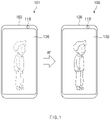
- FIG. 1 illustrates an electronic device capable of capturing an image according to an embodiment.
- an electronic device 100 may generate a preview image based on image data obtained using a camera module (or a camera device) 110 and may output the generated preview image to a display 120.
- the camera module 110 may include, for example, a lens assembly including one or more lens and an image sensor. Each pixel of the image sensor may include a plurality of photo diodes.
- the electronic device 100 may generate phase difference data (or depth data) by optical path differences generated by the plurality of photo diodes (hereinafter, PDs) which share a microlens.
- PDs photo diodes
- the electronic device 100 may adjust a focus on an external object 150 by moving the one or more lenses included in the camera module 110, based on the generated phase difference data.
- the electronic device 100 may display a preview image focusing on the external object on the display 120.
- the camera module 110 is the front camera of the electronic device 100 in FIG. 1 , but not limited thereto.
- the camera module 110 may be disposed on at least one of a rear surface or a side surface of the electronic device 100.
- FIG. 2 illustrates a configuration of an image sensor according to an embodiment.
- an image sensor 200 included in a camera module may include a plurality of pixels. It is illustratively shown that the image sensor 200 outputs a Bayer-patterned image based on a signal generated by a 4PD image sensor in FIG. 2 , but not limited thereto.
- one 210 of a plurality of pixels may include a microlens 205, a color filter 206, a first PD (or a first sub-pixel) (PD1) 211, a second PD (or a second sub-pixel) (PD2) 212, a third PD (or a third sub-pixel) (PD3) 213, and a fourth PD (or a fourth sub-pixel) (PD4) 214.
- the microlens 205 may cover the first to fourth PDs 211, 212, 213, and 214.
- the microlens 205 may adjust a path of an incident light such that a light incident from the outside may arrive at the first to fourth PDs 211, 212, 213, and 214.
- the color filter 206 may be disposed between the microlens 205 and the first to fourth PDs 211, 212, 213, and 214 to pass a light of a specified wavelength range (e.g., a wavelength range corresponding to a green light).
- the color filter 206 may allow only the light of the specified wavelength range in the light passing through the microlens 205 and may limit a light except from the specified wavelength range.
- Each of the first to fourth PDs 211, 212, 213, and 214 may convert the light passing through the microlens 205 and the color filter 206 into an electrical signal.
- the light introduced from the outside may be refracted by the microlens 205 to be changed in progress path.
- the light passing through the microlens 205 may be directly introduced into the PD or may be reflected from a pixel wall W between the PDs to be introduced into the PD.
- FIG. 3 is a drawing illustrating describing an edge direction and AF detection of an object various embodiments.
- an image sensor 200 may include a plurality of pixels.
- One 210 of the plurality of pixels may be covered by one microlens 205.
- the one pixel 210 may include first to fourth PDs 211, 212, 213, and 214.
- a first object 310 disposed in a vertical direction may form an edge 311 in a horizontal direction.
- the two pixels e.g., the first PD 211 and the second PD 212
- Lights incident through the microlens 205 may be differently refracted along a path to be separated from each other. Because the image is formed by the same microlens 205, characteristics and level values of pixels (e.g., the first PD 211 and the second PD 212) located horizontally may be varied for the first object 310 which has an identical focus and is present in an arrangement direction of pixels.
- a second object 320 disposed in the horizontal direction may form an edge 321 in the vertical direction.
- the two pixels e.g., the first PD 211 and the second PD 212
- the two pixels e.g., the first PD 211 and the second PD 212
- Lights incident through the microlens 205 may be differently refracted along a path to be separated from each other. Because the image is formed by the same microlens, characteristics and level values of pixels (e.g., the first PD 211 and the third PD 213) located vertically may be varied for the second object 320 which has an identical focus and is present in an arrangement direction of pixels.
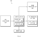
- FIG. 4 illustrates a camera module according to various embodiments.
- a camera module 400 may include an image sensor 410, a controller 420, a memory 430, an image processing unit 440, and an AF processing unit 450.
- FIG. 4 is separated according to a function, but not limited thereto.
- the image sensor 410 and the controller 420 may be integrated into one, or the controller 420 and the AF processing unit 450 may be integrated into one.
- the image sensor 410 may convert a light incident from the outside into an electrical signal.
- the image sensor 410 may be composed of a plurality of pixels.
- Each pixel may include a plurality of PDs.
- PDs a description will be given of, but not limited to, the case where each pixel includes four PDs.
- the image sensor 410 may generate image data for taking a picture or a moving image or image data for displaying a preview screen. Furthermore, the image sensor 410 may generate data (or a signal) (hereinafter, AF data) for performing AF.
- AF data data (or a signal) for performing AF.
- the image sensor 410 when the image sensor 410 is composed of a plurality of PDs sharing the same one microlens, data of the plurality of PDs may be output in an arranged order (e.g., a Bayer pattern).
- the image sensor 410 may generate and output a signal of a format processed through an output mode such as binning to reduce output data.
- the image sensor 410 may output a signal of a format processed by performing image processing in a horizontal/vertical direction or a diagonal direction depending on the arrangement of pixels and if necessary.
- the controller (or a preprocessing unit or a data conversion unit) 420 may process image data or AF data received from the image sensor 410.
- the controller 420 may provide the image data to the image processing unit (e.g., an ISP) 440.
- the controller 420 may temporarily store the AF data in the memory 430 or may deliver the AF data to the AF processing unit 450.
- the controller 420 may detect directionality from the AF data of the image sensor 410 for accurate and simple AF calculation with respect to horizontal and vertical or more directions and may reorder data in a dominant direction, such that the AF processing unit 450 performs AF calculation.
- the controller 420 may maintain AF data in a first direction (e.g., a horizontal direction) and may rotate or reorder AF data in a second direction (e.g., a vertical direction) and may deliver the AF data to the AF processing unit 450.
- a first direction e.g., a horizontal direction
- a second direction e.g., a vertical direction
- the AF processing unit 450 may consistently perform PAF calculation irrespective of directionality.
- the controller 420 may convert and deliver the image data or the AF data, received from the image sensor 410, to the memory 430, the image processing unit 440, or the AF processing unit 450 or may deliver the image data or the AF data to the memory 430, the image processing unit 440, or the AF processing unit 450 without a separate conversion task.
- the controller 420 may include a direction filter 421 or a rotator 422.
- the direction filter 421 may be used to determine a dominant direction among edge directions of an object.
- the rotator 422 may change the direction of the AF data to change the AF data in the form of data capable of being easily processed by the AF processing unit 450.
- the storage unit 430 may store the AF data (or the converted AF data).
- the storage unit 430 may be a DRAM.
- the stored AF data may be delivered to the AF processing unit 450 depending on directionality of an edge.
- the image processing unit (e.g., the ISP) 440 may process image data.
- the received image data may be processed to be displayed as a preview image.
- the AF processing unit 450 may perform AF (PAF) using a phase difference based on the received AF data.
- the AF processing unit 450 may include at least one or more PAF circuits 451. It is illustratively shown that the one PAF circuit is included in FIG. 4 , but not limited thereto.
- the PAF circuit 451 may perform PAF calculation in a specified direction.
- the PAF circuit 451 may process AF data of some (e.g., two) of a plurality of photo diodes (e.g., first to fourth PDs) included in one pixel of the image sensor 410.
- the PAF circuit 451 may perform PAF calculation using AF data extracted from pixels (e.g., the first PD and the second PD or the third PD and the fourth PD) separated horizontally or may perform PAF calculation using AF data extracted from pixels (e.g., the first PD and the third PD or the second PD and the fourth PD) separated vertically.
- AF data extracted from pixels e.g., the first PD and the second PD or the third PD and the fourth PD
- AF circuit 451 may perform PAF calculation using AF data extracted from pixels (e.g., the first PD and the second PD or the third PD and the fourth PD) separated horizontally or may perform PAF calculation using AF data extracted from pixels (e.g., the first PD and the third PD or the second PD and the fourth PD) separated vertically.
- 2PD PAF circuit but not limited thereto.
- the camera module 400 may include a plurality of PAF circuits respectively corresponding to a plurality of edge directions capable of being detected by the image sensor 200.
- a plurality of PAF circuits respectively corresponding to a plurality of edge directions capable of being detected by the image sensor 200.
- two PAF circuits may be included.
- eight PAF circuits may be included.
- the camera module 400 may perform PAF calculation for the plurality of edge directions using one PAF circuit. For example, in case of the edge detection in the vertical/horizontal direction, PAF calculation of the edge in the horizontal direction may be primarily performed and PAF calculation of the edge in the vertical direction may be secondarily performed.
- the camera module 400 may determine a dominant direction among directions of edges using one PAF circuit, perform PAF for one dominant direction, and may fail to, or subsidiarily, proceed with PAF for other directions.
- the controller 420, the image processing unit 440, or the AF processing unit 450 may be performed by a processor (e.g., an AP) of an electronic device (e.g., an electronic device 100 of FIG. 1 ) including the camera module 400.
- a processor e.g., an AP
- an electronic device e.g., an electronic device 100 of FIG. 1
- controller 420, the image processing unit 440, or the AF processing unit 450 may be components (e.g., chips) separated in hardware.
- controller 420, the image processing unit 440, or the AF processing unit 450 may be operations separated in software in the same calculation element.
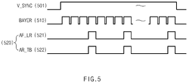
- FIG. 5 is an output timing diagram of image data and AF data according to various embodiments.
- the image sensor 410 may output image data (e.g., a Bayer signal) 510.
- image data e.g., a Bayer signal
- the image sensor 410 may output AF data 520 output at a longer time interval than the image data (e.g., the Bayer signal) 510, together with the image data (e.g., the Bayer signal) 510.
- the image sensor 410 may process AF data in a direction to obtain AF from the image data (e.g., the Bayer signal) 510 and may output the AF data 520 with smaller resolution than the image data (e.g., the Bayer signal) 510 by means of binning or the like.
- the image data e.g., the Bayer signal
- the image sensor 410 may process AF data in a direction to obtain AF from the image data (e.g., the Bayer signal) 510 and may output the AF data 520 with smaller resolution than the image data (e.g., the Bayer signal) 510 by means of binning or the like.
- the AF data AF_LR 521 in the horizontal direction and the AF data AF TB 522 in the vertical direction are output at the same timing in FIG. 5 , but not limited thereto.
- the AF data AF LR 521 in the horizontal direction and the AF data AF TB 522 in the vertical direction are output at different timings.
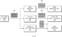
- FIG. 6 illustrates AF processing using two 2PD PAF circuits in a Bayer pattern according to various embodiments.
- Two 2PD PAF circuits are illustratively shown in FIG. 6 , but not limited thereto.
- a 4PD image sensor 610 may include four PDs in one pixel.
- the 4PD image sensor 610 may sequentially read out PDs included in each pixel to generate a multi-PD signal (or raw data) 601.
- An image generator 620 may integrate values of four PDs included in one pixel to generate image data 602.
- the image generator 620 may transmit the image data 602 to an image processing unit (e.g., an ISP) 625.
- an image processing unit e.g., an ISP
- a first AF data generator 630 may deliver AF data 603 in a first direction (e.g., a horizontal direction) in the multi-PD signal 601 to a first PAF circuit 635.
- a second AF data generator 640 may deliver AF data 604 in a second direction (e.g., a vertical direction) in the multi-PD signal 601 to a second PAF circuit 645.
- a second direction e.g., a vertical direction
- Each of the first PAF circuit 635 and the second PAF circuit 645 may perform PAF calculation for a different direction.
- the first PAF circuit 635 and the second PAF circuit 645 may perform AF calculation at the same time. As a result, quick and accurate AF may be performed.
- AF data for eight directions may be simultaneously and separately processed by eight PAF circuits.
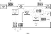
- FIG. 7A illustrates AF processing using one 2PD PAF circuit in a Bayer pattern according to various embodiments.
- a 4PD image sensor 710 may include four PDs in one pixel.
- the 4PD image sensor 710 may sequentially read out PDs included in each pixel to generate a multi-PD signal (or raw data) 701.
- An image generator 720 may integrate values of four PDs included in one pixel to generate main image data 702.
- the image generator 720 may transmit the image data 702 to an image processing unit (e.g., an ISP) 725.
- an image processing unit e.g., an ISP
- An AF data generator 730 may convert the multi-PD signal 701 into AF data 703 capable of being processed by a PAF circuit 735 and may store the AF data 703 in a memory (e.g., a DRAM) 750.
- a memory e.g., a DRAM
- vertical data 703a and horizontal data 703b may be stored.
- the memory 750 may store the AF data 703.
- a storage unit 740 may be a memory buffer included in a camera module or a memory area formed independently of the camera module.
- the PAF circuit 735 may process the AF data 703 stored for each direction from the memory 750. According to an embodiment, the PAF circuit 735 may sequentially process the AF data 703 depending on a direction. For example, the PAF circuit 735 may primarily process the horizontal data 703b and may secondarily process the vertical data 703a.
- the rotator 760 may rotate and deliver signals in the other directions except for a first direction (e.g., a horizontal direction) to the PAF circuit 735.
- a first direction e.g., a horizontal direction
- the vertical data 703a may rotate at 90 degrees to be provided to the PAF circuit 735 (703a-1).
- the horizontal data 703b and the converted vertical data 703a-1 may have a data structure similar to each other, and the calculation process of the PAF circuit 735 may be simplified.
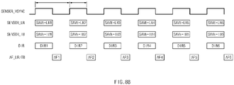
- FIG. 7B is an output timing diagram of processing image data and AF data according to various embodiments.
- the image sensor 710 may store AF data SAVE_LR and SAVE TB at a specified time interval.
- a PAF circuit 735 may start PAF using the horizontal data SAVE LR at a time when the storage of the horizontal data SAVE LR is completed.
- PAF (AF_LR) for a horizontal direction may be completed at the same time that the storage of the horizontal data SAVE LR is ended (or as a portion of the storage of the horizontal data SAVE LR is delayed).
- the PAF circuit 735 may start PAF (AF_TB) using the stored vertical data SAVE TB.
- PAF using the vertical data SAVE TB may proceed in a state where the vertical data SAVE TB in stored (a state where a timing signal SENSOR VSYNC is low).
- AF data may be converted into a size smaller than image data to be output. It is possible to process PAF (AF TB) within a relatively short time using the PAF (AF LR) for the horizontal direction or the vertical data SAVE TB. It may be possible to proceed with PAF (AF_TB), after the readout of all frames is completed because of having a different readout direction, using the vertical data SAVE TB.
- the PAF circuit 735 may perform PAF calculation for a plurality of directions in the state where the timing signal SENSOR VSYNC is low.
- the PAF circuit 735 may perform PAF calculation for the plurality of directions in a vertical direction, a 45-degree direction, and a 125-degree direction in the state where the timing signal SENSOR VSYNC is low.
- FIG. 8A illustrates AF processing using a direction filter in a Bayer pattern according to various embodiments.
- a 4PD image sensor 810 may include four PDs in one pixel.
- the 4PD image sensor 810 may sequentially read out PDs included in each pixel to generate a multi-PD signal (or raw data) 801.
- An image generator 820 may integrate values of four PDs included in one pixel to generate main image data 802.
- the image generator 820 may transmit the image data 802 to an image processing unit (e.g., an ISP) 825.
- an image processing unit e.g., an ISP
- An AF data generator 830 may convert the multi-PD signal 801 into AF data 803 capable of being processed by a PAF circuit 835 and may store the AF data 803 in a memory (e.g., a DRAM) 850.
- a memory e.g., a DRAM
- vertical data 803a and horizontal data 803b may be stored.
- the memory 850 may store the AF data 803.
- a storage unit 840 may be a memory buffer included in a camera module or a memory area formed independently of the camera module.
- a direction filter 860 may detect an edge direction, using the AF data 803.
- the PAF circuit 835 may process AF data for one direction among the AF data 803 stored for each direction from the memory 850.
- the PAF circuit 835 may perform one PAF calculation for one direction determined by means of the direction filter 860.
- the vertical data 803a which is one direction according to an arrangement direction of an edge (or an arrangement direction of an object) may be selected between the horizontal data 703a and the vertical data 703b.
- the PAF circuit 835 may rotate the vertical data 803a by means of a rotator 860 (803a-1) to perform one PAF calculation.
- the rotator 860 may rotate and deliver signals in the other directions except for a first direction (e.g., a horizontal direction) to the PAF circuit 835.
- a first direction e.g., a horizontal direction
- the vertical data 803a may rotate at 90 degrees to be delivered to the PAF circuit 835 (803a-1).
- the horizontal data 803b and the converted vertical data 803a-1 may have a data structure similar to each other, and the calculation process of the PAF circuit 835 may be simplified.
- FIG. 8B is an output timing diagram of selective AF processing using a direction filter according to various embodiments.
- the image sensor 810 may store AF data SAVE LR and SAVE TB at a specified time interval.
- a PAF circuit 835 may perform edge detection (or directionality determination of an image) using a direction filter 870.
- the PAF circuit 835 may proceed with PAF for one direction selected by means of the direction filter 870. In a state where the timing signal SENSOR VSYNC is low, one PAF may proceed.
- FIG. 9 illustrates AF processing using two 2PD PAF circuits in a processing pattern according to various embodiments.
- the two 2PD PAF circuits are illustratively shown in FIG. 9 , but not limited thereto.
- a 4PD image sensor 910 may include four PDs in one pixel.
- the 4PD image sensor 910 may integrate values of four PDs included in one pixel to generate image data 902.
- the 4PD image sensor 910 may transmit the image data 902 to an image processing unit (e.g., an ISP) 925.
- an image processing unit e.g., an ISP
- the 4PD image sensor 910 may deliver first processing data 903 obtained by processing AF data in a first direction (e.g., a horizontal direction) to a first PAF circuit 935.
- a first direction e.g., a horizontal direction
- the 4PD image sensor 910 may deliver second processing data 904 obtained by processing AF data in a second direction (e.g., a vertical direction) to a second PAF circuit 945.
- a second direction e.g., a vertical direction
- Each of the first PAF circuit 935 and the second PAF circuit 945 may perform PAF calculation for a different direction.
- the first PAF circuit 935 and the second PAF circuit 945 may perform AF calculation at the same time. As a result, quick and accurate AF may be performed.
- AF data for eight directions may be simultaneously and separately processed by eight PAF circuits.
- FIG. 10 illustrates AF processing using one 2PD PAF circuit in a processing pattern according to various embodiments.
- a 4PD image sensor 1010 may include four PDs in one pixel.
- the 4PD image sensor 1010 may integrate values of four PDs included in one pixel to generate image data 1002.
- the 4PD image sensor 1010 may transmit the image data 1002 to an image processing unit (e.g., an ISP) 1025.
- an image processing unit e.g., an ISP
- the 4PD image sensor 1010 may store first processing data 903 obtained by processing AF data in a first direction (e.g., a horizontal direction) in a memory (e.g., a DRAM) 1050.
- first direction e.g., a horizontal direction
- a memory e.g., a DRAM
- vertical data 1003a and horizontal data 1003b may be stored.
- the memory 1050 may store the AF data 1003.
- a storage unit 1040 may be a memory buffer included in a camera module or a memory area formed independently of the camera module.
- a PAF circuit 1035 may process the AF data 1003 stored for each direction from the memory 1050. According to an embodiment, the PAF circuit 1035 may sequentially process the AF data 1003 depending on a direction. For example, the PAF circuit 1035 may primarily process the horizontal data 1003b and may secondarily process the vertical data 1003a.
- a rotator 1060 may rotate and deliver signals in the other directions except for the first direction (e.g., the horizontal direction) to the PAF circuit 1035.
- the vertical data 1003a may rotate at 90 degrees to be provided to the PAF circuit 1035 (1003a-1).
- the horizontal data 1003b and the converted vertical data 1003a-1 may have a data structure similar to each other, and the calculation process of the PAF circuit 1035 may be simplified.
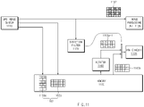
- FIG. 11 illustrates AF processing using a direction filter in a processing pattern according to various embodiments.
- a 4PD image sensor 1110 may include 4 PDs in one pixel.
- the 4PD image sensor 1110 may integrate values of four PDs included in one pixel to generate image data 1102.
- the 4PD image sensor 1110 may transmit the image data 1102 to an image processing unit (e.g., an ISP) 1125.
- an image processing unit e.g., an ISP
- the 4PD image sensor 1110 may store first processing data 1103 obtained by processing AF data in a first direction (e.g., a horizontal direction) in a memory (e.g., a DRAM) 1150.
- first direction e.g., a horizontal direction
- a memory e.g., a DRAM
- vertical data 1103a and horizontal data 1103b may be stored.
- the memory 1150 may store the AF data 1103.
- a storage unit 1140 may be a memory buffer included in a camera module or a memory area formed independently of the camera module.
- a direction filter 1160 may detect an edge direction, using the AF data 1103.
- the PAF circuit 1135 may process AF data for one direction among the AF data 1103 stored for each direction from the memory 1150.
- the PAF circuit 1135 may perform one PAF calculation for one direction determined by means of the direction filter 1160.
- the vertical data 1103a which is one direction according to an arrangement direction of an edge (or an arrangement direction of an object) may be selected between the horizontal data 1103a and the vertical data 1103b.
- the PAF circuit 1135 may rotate the vertical data 1103a by means of a rotator 1160 (1103a-1) to perform one PAF calculation.
- the rotator 1160 may rotate and deliver signals in the other directions except for the first direction (e.g., the horizontal direction) to the PAF circuit 1135.
- the vertical data 1103a may rotate at 90 degrees to be provided to the PAF circuit 1135 (1103a-1).
- the horizontal data 1103b and the converted vertical data 1103a-1 may have a data structure similar to each other, and the calculation process of the PAF circuit 1135 may be simplified.
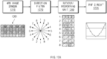
- FIGS. 12A and 12B are drawings illustrating detecting an edge in a plurality of directions by means of a direction filter and performing PAF calculation according to various embodiments.
- a 4PD image sensor 1210 may include four PDs in one pixel.
- the 4PD image sensor 1210 may sequentially read out PDs included in each pixel to generate a multi-PD signal (or raw data) 1201.
- a direction filter 1270 may compare detection values for the plurality of directions, in AF data using the multi-PD signal (or the raw data), to detect directionality (an edge direction) of an image. For example, when data of a first portion and a second portion are changed to a specified value or more by an external object among all pixels of the AF data, it may be determined that a boundary (edge) of the first portion and the second portion is formed.
- data of a first portion 1201a1 and a second portion 1201a2 of the 4PD image sensor 1210 may be changed to the specified value or more by a first object 1251.
- the direction filter 1270 may compare values of image data to detect an edge direction 1251a perpendicular to a boundary of the first portion 1201al and the second portion 1201a2 as a fifth direction (0 degree).
- data of a first portion 1201b1 and a second portion 1201b2 of the 4PD image sensor 1210 may be changed to the specified value or more by a second object 1252.
- the direction filter 1270 may compare values of image data to detect an edge direction 1252a perpendicular to a boundary of the first portion 1201b1 and the second portion 1201b2 as a third direction (45 degrees).
- data of a first portion 1201c1 and a second portion 1201c2 of the 4PD image sensor 1210 may be changed to the specified value or more by a third object 1253.
- the direction filter 1270 may compare values of image data to detect an edge direction 1253a perpendicular to a boundary of the first portion 1201c1 and the second portion 1201c2 as a first direction (90 degrees).
- data of a first portion 1201d1 and a second portion 1201d2 of the 4PD image sensor 1210 may be changed to the specified value or more by a fourth object 1254.
- the direction filter 1270 may compare values of image data to detect an edge direction 1254a perpendicular to a boundary of the first portion 1201d1 and the second portion 1201d2 as a seventh direction (135 degrees).
- a reordering unit 1280 may rotate or reorder AF data for each direction (or a direction where an edge is mainly disposed).
- the reordering unit 1280 may rotate or reorder AF data in an edge direction 1251a, 1252a, 1253a, or 1254a perpendicular to the boundary of the first portion 1201a1, 1201b1, 1201c1, or 1201dl and the second portion 1201a2, 1201b2, 1201c2, or 1201d2.
- the PAF circuit 1235 may perform PAF calculation depending on directionality of an edge.
- the PAF circuit 1235 performs determined calculation irrespective of information about directionality, it may perform PAF calculation depending on directionality of an edge to obtain a PAF result with high reliability.
- the PAF circuit 1235 may extract a statistical value for each direction and may perform AF determination.
- FIG. 13 is a block diagram of an electronic device 1301 in a network environment 1300 according to various embodiments of the present disclosure.
- the electronic device may be a device of various types.
- the electronic device includes, for example, at least one of a portable communication device (e.g., smartphone), a computer device (e.g., a personal digital assistant; PDA), a tablet PC, a laptop PC (a desktop PC, a workstation, or a server), a portable multimedia device (e.g., an e-book reader or an MP3 player), a portable medical device devices (e.g., heartbeat measuring devices, blood glucose monitoring devices, blood pressure measuring devices, and body temperature measuring devices), a camera, or a wearable device.
- a portable communication device e.g., smartphone
- PDA personal digital assistant
- PDA personal digital assistant
- tablet PC e.g., a laptop PC (a desktop PC, a workstation, or a server
- a portable multimedia device e.g., an e
- the wearable device may include at least one of an accessory type (e.g., watches, rings, bracelets, anklets, necklaces, glasses, contact lens, or head-mounted-devices (HMDs)), a fabric or garment-integrated type (e.g., an electronic apparel), a body-attached type (e.g., a skin pad or tattoos), or a bio-implantable type (e.g., an implantable circuit).
- an accessory type e.g., watches, rings, bracelets, anklets, necklaces, glasses, contact lens, or head-mounted-devices (HMDs)
- a fabric or garment-integrated type e.g., an electronic apparel
- a body-attached type e.g., a skin pad or tattoos
- a bio-implantable type e.g., an implantable circuit
- the electronic device may include at least one of, for example, televisions (TVs), digital versatile disk (DVD) players, audios, audio accessory devices (e.g., speakers, headphones, or headsets), refrigerators, air conditioners, cleaners, ovens, microwave ovens, washing machines, air cleaners, set-top boxes, home automation control panels, security control panels, game consoles, electronic dictionaries, electronic keys, camcorders, or electronic picture frames.
- TVs televisions
- DVD digital versatile disk
- audio accessory devices e.g., speakers, headphones, or headsets
- refrigerators air conditioners, cleaners, ovens, microwave ovens, washing machines, air cleaners, set-top boxes, home automation control panels, security control panels, game consoles, electronic dictionaries, electronic keys, camcorders, or electronic picture frames.
- the electronic device may include at least one of navigation devices, satellite navigation system (e.g., Global Navigation Satellite System (GNSS)), event data recorders (EDRs) (e.g., black box for a car, a ship, or a plane), vehicle infotainment devices (e.g., head-up display for vehicle), industrial or home robots, drones, automatic teller's machines (ATMs), points of sales (POSs), measuring instruments (e.g., water meters, electricity meters, or gas meters), or internet of things (e.g., light bulbs, sprinkler devices, fire alarms, thermostats, or street lamps).
- satellite navigation system e.g., Global Navigation Satellite System (GNSS)
- EDRs event data recorders
- vehicle infotainment devices e.g., head-up display for vehicle
- industrial or home robots drones, automatic teller's machines (ATMs), points of sales (POSs), measuring instruments (e.g., water meters, electricity meters, or gas meters), or internet of things (
- the electronic device may not be limited to the above-described devices, and may provide functions of a plurality of devices like smartphones which has measurement function of personal biometric information (e.g., heart rate or blood glucose).
- personal biometric information e.g., heart rate or blood glucose
- the term "user” may refer to a person who uses an electronic device or may refer to a device (e.g., an artificial intelligence electronic device) that uses the electronic device.
- Fig. 13 is a block diagram illustrating an electronic device 1301 (e.g., the foldable electronic device 101 of FIG. 1 ) in a network environment 1300 according to various embodiments.
- the electronic device 1301 in the network environment 1300 may communicate with an electronic device 1302 via a first network 1398 (e.g., a short-range wireless communication network), or at least one of an electronic device 1304 or a server 1308 via a second network 1399 (e.g., a long-range wireless communication network).
- the electronic device 1301 may communicate with the electronic device 1304 via the server 1308.
- the electronic device 1301 may include a processor 1320, memory 1330, an input module 1350, a sound output module 1355, a display module 1360, an audio module 1370, a sensor module 1376, an interface 1377, a connecting terminal 1378, a haptic module 1379, a camera module 1380, a power management module 1388, a battery 1389, a communication module 1390, a subscriber identification module (SIM) 1396, or an antenna module 1397.
- at least one of the components e.g., the connecting terminal 1378) may be omitted from the electronic device 1301, or one or more other components may be added in the electronic device 1301.
- some of the components e.g., the sensor module 1376, the camera module 1380, or the antenna module 1397) may be implemented as a single component (e.g., the display module 1360).
- the processor 1320 may execute, for example, software (e.g., a program 1340) to control at least one other component (e.g., a hardware or software component) of the electronic device 1301 coupled with the processor 1320, and may perform various data processing or computation. According to one embodiment, as at least part of the data processing or computation, the processor 1320 may store a command or data received from another component (e.g., the sensor module 1376 or the communication module 1390) in volatile memory 1332, process the command or the data stored in the volatile memory 1332, and store resulting data in non-volatile memory 1334.
- software e.g., a program 1340
- the processor 1320 may store a command or data received from another component (e.g., the sensor module 1376 or the communication module 1390) in volatile memory 1332, process the command or the data stored in the volatile memory 1332, and store resulting data in non-volatile memory 1334.
- the processor 1320 may include a main processor 1321 (e.g., a central processing unit (CPU) or an application processor (AP)), or an auxiliary processor 1323 (e.g., a graphics processing unit (GPU), a neural processing unit (NPU), an image signal processor (ISP), a sensor hub processor, or a communication processor (CP)) that is operable independently from, or in conjunction with, the main processor 1321.
- a main processor 1321 e.g., a central processing unit (CPU) or an application processor (AP)
- auxiliary processor 1323 e.g., a graphics processing unit (GPU), a neural processing unit (NPU), an image signal processor (ISP), a sensor hub processor, or a communication processor (CP)
- the auxiliary processor 1323 may be adapted to consume less power than the main processor 1321, or to be specific to a specified function.
- the auxiliary processor 1323 may be implemented as separate from, or as part of the main processor 1321.
- the auxiliary processor 1323 may control at least some of functions or states related to at least one component (e.g., the display module 1360, the sensor module 1376, or the communication module 1390) among the components of the electronic device 1301, instead of the main processor 1321 while the main processor 1321 is in an inactive (e.g., sleep) state, or together with the main processor 1321 while the main processor 1321 is in an active state (e.g., executing an application).
- the auxiliary processor 1323 e.g., an image signal processor or a communication processor
- the auxiliary processor 1323 may include a hardware structure specified for artificial intelligence model processing.
- An artificial intelligence model may be generated by machine learning. Such learning may be performed, e.g., by the electronic device 1301 where the artificial intelligence is performed or via a separate server (e.g., the server 1308). Learning algorithms may include, but are not limited to, e.g., supervised learning, unsupervised learning, semi-supervised learning, or reinforcement learning.
- the artificial intelligence model may include a plurality of artificial neural network layers.
- the artificial neural network may be a deep neural network (DNN), a convolutional neural network (CNN), a recurrent neural network (RNN), a restricted boltzmann machine (RBM), a deep belief network (DBN), a bidirectional recurrent deep neural network (BRDNN), deep Q-network or a combination of two or more thereof but is not limited thereto.
- the artificial intelligence model may, additionally or alternatively, include a software structure other than the hardware structure.
- the memory 1330 may store various data used by at least one component (e.g., the processor 1320 or the sensor module 1376) of the electronic device 1301.
- the various data may include, for example, software (e.g., the program 1340) and input data or output data for a command related thererto.
- the memory 1330 may include the volatile memory 1332 or the non-volatile memory 1334.
- the program 1340 may be stored in the memory 1330 as software, and may include, for example, an operating system (OS) 1342, middleware 1344, or an application 1346.
- OS operating system
- middleware middleware
- application application
- the input module 1350 may receive a command or data to be used by another component (e.g., the processor 1320) of the electronic device 1301, from the outside (e.g., a user) of the electronic device 1301.
- the input module 1350 may include, for example, a microphone, a mouse, a keyboard, a key (e.g., a button), or a digital pen (e.g., a stylus pen).
- the sound output module 1355 may output sound signals to the outside of the electronic device 1301.
- the sound output module 1355 may include, for example, a speaker or a receiver.
- the speaker may be used for general purposes, such as playing multimedia or playing record.
- the receiver may be used for receiving incoming calls. According to an embodiment, the receiver may be implemented as separate from, or as part of the speaker.
- the display module 1360 may visually provide information to the outside (e.g., a user) of the electronic device 1301.
- the display module 1360 may include, for example, a display, a hologram device, or a projector and control circuitry to control a corresponding one of the display, hologram device, and projector.
- the display module 1360 may include a touch sensor adapted to detect a touch, or a pressure sensor adapted to measure the intensity of force incurred by the touch.
- the audio module 1370 may convert a sound into an electrical signal and vice versa. According to an embodiment, the audio module 1370 may obtain the sound via the input module 1350, or output the sound via the sound output module 1355 or a headphone of an external electronic device (e.g., an electronic device 1302) directly (e.g., wiredly) or wirelessly coupled with the electronic device 1301.
- an external electronic device e.g., an electronic device 1302
- directly e.g., wiredly
- wirelessly e.g., wirelessly
- the sensor module 1376 may detect an operational state (e.g., power or temperature) of the electronic device 1301 or an environmental state (e.g., a state of a user) external to the electronic device 1301, and then generate an electrical signal or data value corresponding to the detected state.
- the sensor module 1376 may include, for example, a gesture sensor, a gyro sensor, an atmospheric pressure sensor, a magnetic sensor, an acceleration sensor, a grip sensor, a proximity sensor, a color sensor, an infrared (IR) sensor, a biometric sensor, a temperature sensor, a humidity sensor, or an illuminance sensor.
- the interface 1377 may support one or more specified protocols to be used for the electronic device 1301 to be coupled with the external electronic device (e.g., the electronic device 1302) directly (e.g., wiredly) or wirelessly.
- the interface 1377 may include, for example, a high definition multimedia interface (HDMI), a universal serial bus (USB) interface, a secure digital (SD) card interface, or an audio interface.
- HDMI high definition multimedia interface
- USB universal serial bus
- SD secure digital
- a connecting terminal 1378 may include a connector via which the electronic device 1301 may be physically connected with the external electronic device (e.g., the electronic device 1302).
- the connecting terminal 1378 may include, for example, a HDMI connector, a USB connector, a SD card connector, or an audio connector (e.g., a headphone connector).
- the haptic module 1379 may convert an electrical signal into a mechanical stimulus (e.g., a vibration or a movement) or electrical stimulus which may be recognized by a user via his tactile sensation or kinesthetic sensation.
- the haptic module 1379 may include, for example, a motor, a piezoelectric element, or an electric stimulator.
- the camera module 1380 may capture a still image or moving images.
- the camera module 1380 may include one or more lenses, image sensors, image signal processors, or flashes.
- the power management module 1388 may manage power supplied to the electronic device 1301. According to one embodiment, the power management module 1388 may be implemented as at least part of, for example, a power management integrated circuit (PMIC).
- PMIC power management integrated circuit
- the battery 1389 may supply power to at least one component of the electronic device 1301.
- the battery 1389 may include, for example, a primary cell which is not rechargeable, a secondary cell which is rechargeable, or a fuel cell.
- the communication module 1390 may support establishing a direct (e.g., wired) communication channel or a wireless communication channel between the electronic device 1301 and the external electronic device (e.g., the electronic device 1302, the electronic device 1304, or the server 1308) and performing communication via the established communication channel.
- the communication module 1390 may include one or more communication processors that are operable independently from the processor 1320 (e.g., the application processor (AP)) and supports a direct (e.g., wired) communication or a wireless communication.
- AP application processor
- the communication module 1390 may include a wireless communication module 1392 (e.g., a cellular communication module, a short-range wireless communication module, or a global navigation satellite system (GNSS) communication module) or a wired communication module 1394 (e.g., a local area network (LAN) communication module or a power line communication (PLC) module).
- a wireless communication module 1392 e.g., a cellular communication module, a short-range wireless communication module, or a global navigation satellite system (GNSS) communication module
- GNSS global navigation satellite system
- wired communication module 1394 e.g., a local area network (LAN) communication module or a power line communication (PLC) module.
- LAN local area network
- PLC power line communication
- a corresponding one of these communication modules may communicate with the external electronic device via the first network 1398 (e.g., a short-range communication network, such as Bluetooth TM , wireless-fidelity (Wi-Fi) direct, or infrared data association (IrDA)) or the second network 1399 (e.g., a long-range communication network, such as a cellular network, the Internet, or a computer network (e.g., LAN or wide area network (WAN)).
- the first network 1398 e.g., a short-range communication network, such as Bluetooth TM , wireless-fidelity (Wi-Fi) direct, or infrared data association (IrDA)
- the second network 1399 e.g., a long-range communication network, such as a cellular network, the Internet, or a computer network (e.g., LAN or wide area network (WAN)
- These various types of communication modules may be implemented as a single component (e.g., a single chip), or may be implemented as multi
- the wireless communication module 1392 may identify and authenticate the electronic device 1301 in a communication network, such as the first network 1398 or the second network 1399, using subscriber information (e.g., international mobile subscriber identity (IMSI)) stored in the subscriber identification module 1396.
- subscriber information e.g., international mobile subscriber identity (IMSI)
- the antenna module 1397 may transmit or receive a signal or power to or from the outside (e.g., the external electronic device) of the electronic device 1301.
- the antenna module 1397 may include an antenna including a radiating element composed of a conductive material or a conductive pattern formed in or on a substrate (e.g., PCB).
- the antenna module 1397 may include a plurality of antennas. In such a case, at least one antenna appropriate for a communication scheme used in the communication network, such as the first network 1398 or the second network 1399, may be selected, for example, by the communication module 1390 (e.g., the wireless communication module 1392) from the plurality of antennas.
- the signal or the power may then be transmitted or received between the communication module 1390 and the external electronic device via the selected at least one antenna.
- another component e.g., a radio frequency integrated circuit (RFIC)
- RFIC radio frequency integrated circuit
- At least some of the above-described components may be coupled mutually and communicate signals (e.g., commands or data) therebetween via an inter-peripheral communication scheme (e.g., a bus, general purpose input and output (GPIO), serial peripheral interface (SPI), or mobile industry processor interface (MIPI)).
- an inter-peripheral communication scheme e.g., a bus, general purpose input and output (GPIO), serial peripheral interface (SPI), or mobile industry processor interface (MIPI)
- commands or data may be transmitted or received between the electronic device 1301 and the external electronic device 1304 via the server 1308 coupled with the second network 1399.
- Each of the electronic devices 1302 and 1304 may be a device of a same type as, or a different type, from the electronic device 1301.
- all or some of operations to be executed at the electronic device 1301 may be executed at one or more of the external electronic devices 1302, 1304, or 1308.
- the electronic device 1301, instead of, or in addition to, executing the function or the service may request the one or more external electronic devices to perform at least part of the function or the service.
- the one or more external electronic devices receiving the request may perform the at least part of the function or the service requested, or an additional function or an additional service related to the request, and transfer an outcome of the performing to the electronic device 1301.
- the electronic device 1301 may provide the outcome, with or without further processing of the outcome, as at least part of a reply to the request.
- a cloud computing, distributed computing, or client-server computing technology may be used, for example.
- FIG. 14 is a block diagram 1400 illustrating the camera module 1380 according to various embodiments.
- the camera module 1380 may include a lens assembly 1410, a flash 1420, an image sensor 1430, an image stabilizer 1440, memory 1450 (e.g., buffer memory), or an image signal processor 1460.
- the lens assembly 1410 may collect light emitted or reflected from an object whose image is to be taken.
- the lens assembly 1410 may include one or more lenses.
- the camera module 1380 may include a plurality of lens assemblies 1410. In such a case, the camera module 1380 may form, for example, a dual camera, a 360-degree camera, or a spherical camera.
- Some of the plurality of lens assemblies 1410 may have the same lens attribute (e.g., view angle, focal length, auto-focusing, f number, or optical zoom), or at least one lens assembly may have one or more lens attributes different from those of another lens assembly.
- the lens assembly 1410 may include, for example, a wide-angle lens or a telephoto lens.
- the flash 1420 may emit light that is used to reinforce light reflected from an object.
- the flash 1420 may include one or more light emitting diodes (LEDs) (e.g., a red-green-blue (RGB) LED, a white LED, an infrared (IR) LED, or an ultraviolet (UV) LED) or a xenon lamp.
- LEDs light emitting diodes
- the image sensor 1430 may obtain an image corresponding to an object by converting light emitted or reflected from the object and transmitted via the lens assembly 1410 into an electrical signal.
- the image sensor 1430 may include one selected from image sensors having different attributes, such as a RGB sensor, a black-and-white (BW) sensor, an IR sensor, or a UV sensor, a plurality of image sensors having the same attribute, or a plurality of image sensors having different attributes.
- Each image sensor included in the image sensor 1430 may be implemented using, for example, a charged coupled device (CCD) sensor or a complementary metal oxide semiconductor (CMOS) sensor.
- CCD charged coupled device
- CMOS complementary metal oxide semiconductor
- the image stabilizer 1440 may move the image sensor 1430 or at least one lens included in the lens assembly 1410 in a particular direction, or control an operational attribute (e.g., adjust the read-out timing) of the image sensor 1430 in response to the movement of the camera module 1380 or the electronic device 1301 including the camera module 1380. This allows compensating for at least part of a negative effect (e.g., image blurring) by the movement on an image being captured.
- the image stabilizer 1440 may sense such a movement by the camera module 1380 or the electronic device 1301 using a gyro sensor (not shown) or an acceleration sensor (not shown) disposed inside or outside the camera module 1380.
- the image stabilizer 1440 may be implemented, for example, as an optical image stabilizer.
- the memory 1450 may store, at least temporarily, at least part of an image obtained via the image sensor 1430 for a subsequent image processing task. For example, if image capturing is delayed due to shutter lag or multiple images are quickly captured, a raw image obtained (e.g., a Bayer-patterned image, a high-resolution image) may be stored in the memory 1450, and its corresponding copy image (e.g., a low-resolution image) may be previewed via the display device 1360.
- a raw image obtained e.g., a Bayer-patterned image, a high-resolution image
- its corresponding copy image e.g., a low-resolution image
- the memory 1450 may be configured as at least part of the memory 1330 or as a separate memory that is operated independently from the memory 1330.
- the image signal processor 1460 may perform one or more image processing with respect to an image obtained via the image sensor 1430 or an image stored in the memory 1450.
- the one or more image processing may include, for example, depth map generation, three-dimensional (3D) modeling, panorama generation, feature point extraction, image synthesizing, or image compensation (e.g., noise reduction, resolution adjustment, brightness adjustment, blurring, sharpening, or softening).
- the image signal processor 1460 may perform control (e.g., exposure time control or read-out timing control) with respect to at least one (e.g., the image sensor 1430) of the components included in the camera module 1380.
- An image processed by the image signal processor 1460 may be stored back in the memory 1450 for further processing, or may be provided to an external component (e.g., the memory 1330, the display device 1360, the electronic device 1302, the electronic device 1304, or the server 1308) outside the camera module 1380.
- the image signal processor 1460 may be configured as at least part of the processor 1320, or as a separate processor that is operated independently from the processor 1320. If the image signal processor 1460 is configured as a separate processor from the processor 1320, at least one image processed by the image signal processor 1460 may be displayed, by the processor 1320, via the display device 1360 as it is or after being further processed.
- the electronic device 1301 may include a plurality of camera modules 1380 having different attributes or functions.
- at least one of the plurality of camera modules 1380 may form, for example, a wide-angle camera and at least another of the plurality of camera modules1380 may form a telephoto camera.
- at least one of the plurality of camera modules 1380 may form, for example, a front camera and at least another of the plurality of camera modules1380 may form a rear camera.
- An electronic device may include an image sensor (e.g., an image sensor 200 of FIG. 2 or an image sensor 1430 of FIG. 14 ) including a plurality of pixels, an AF processing unit (e.g., an AF processing unit 450 of FIG. 4 ) for performing calculation for performing auto focus based on a phase difference, a memory (e.g., a memory 430 of FIG. 4 , a memory 1330 of FIG. 13 , or a memory 1450 of FIG. 14 ), and a controller (e.g., a controller 420 of FIG.
- an image sensor e.g., an image sensor 200 of FIG. 2 or an image sensor 1430 of FIG. 14
- an AF processing unit e.g., an AF processing unit 450 of FIG. 4
- a memory e.g., a memory 430 of FIG. 4 , a memory 1330 of FIG. 13 , or a memory 1450 of FIG. 14
- controller e.g., a controller 420 of FIG
- Each pixel included in the plurality of pixels may include a plurality of photo diodes and a microlens for covering the plurality of photo diodes.
- the controller e.g., the controller 420 of FIG. 4
- may provide the AF processing unit e.g., the AF processing unit 450 of FIG.
- the AF processing unit may perform first phase auto focus (PAF) calculation based on the first AF data or may perform second PAF calculation based on the second AF data.
- PAF phase auto focus
- the AF processing unit may include a first AF circuit and a second AF circuit.
- the second AF circuit may perform the second phase auto focus (PAF) calculation, while the first AF circuit performs the first phase auto focus (PAF) calculation.
- PAF phase auto focus
- the AF processing unit may include one AF circuit.
- the AF circuit may perform the first phase auto focus (PAF) calculation and may perform the second PAF, when the first phase auto focus (PAF) calculation is ended.
- PAF phase auto focus
- the controller may rotate the second AF data to correspond to the first direction and may provide the AF processing unit (e.g., the AF processing unit 450 of FIG. 4 ) with the second AF data.
- the AF processing unit may select one of the first direction or the second direction by means of a direction filter and may perform PAF calculation for AF data corresponding to the selected direction.
- the AF controller may store the first AF data or the second AF data in the memory (e.g., the memory 430 of FIG. 4 , the memory 1330 of FIG. 13 , or the memory 1450 of FIG. 14 ).
- the AF controller e.g., the controller 420 of FIG. 4
- the AF controller may provide the AF processing unit (e.g., the AF processing unit 450 of FIG. 4 ) with the first AF data or the second AF data with a Bayer pattern or a processing pattern.
- the AF processing unit may perform the first PAF calculation during a process where the first AF data and the second AF data are stored in the memory (e.g., the memory 430 of FIG. 4 , the memory 1330 of FIG. 13 , or the memory 1450 of FIG. 14 ) and may calculate the second PAF calculation after the process is ended.
- the memory e.g., the memory 430 of FIG. 4 , the memory 1330 of FIG. 13 , or the memory 1450 of FIG. 14
- the AF processing unit may perform the first PAF calculation while the first AF data and the second AF data are read out by means of the image sensor (e.g., the image sensor 200 of FIG. 2 or the image sensor 1430 of FIG. 14 ) and may perform the second PAF calculation after the readout is ended.
- the image sensor e.g., the image sensor 200 of FIG. 2 or the image sensor 1430 of FIG. 14
- the image sensor (e.g., the image sensor 200 of FIG. 2 or the image sensor 1430 of FIG. 14 ) may be formed such that one microlens covers four photo diodes.
- the AF processing unit (e.g., the AF processing unit 450 of FIG. 4 ) may compare measurement values of the two photo diodes to perform PAF calculation.
- An electronic device may include an image sensor (e.g., an image sensor 200 of FIG. 2 or an image sensor 1430 of FIG. 14 ) including a plurality of pixels, wherein each pixel included in the plurality of pixels includes a plurality of photo diodes and a microlens for covering the plurality of photo diodes, an AF processing unit (e.g., an AF processing unit 450 of FIG. 4 ) for performing calculation for performing auto focus based on a phase difference, a memory (e.g., a memory 430 of FIG. 4 , a memory 1330 of FIG. 13 , or a memory 1450 of FIG.
- an image sensor e.g., an image sensor 200 of FIG. 2 or an image sensor 1430 of FIG. 14
- an AF processing unit e.g., an AF processing unit 450 of FIG. 4
- a memory e.g., a memory 430 of FIG. 4 , a memory 1330 of FIG. 13 , or a memory 1450 of
- a controller e.g., a controller 420 of FIG. 4 for delivering data obtained by the image sensor (e.g., the image sensor 200 of FIG. 2 or the image sensor 1430 of FIG. 14 ) to the AF processing unit or the memory (e.g., the memory 430 of FIG. 4 , the memory 1330 of FIG. 13 , or the memory 1450 of FIG. 14 ).
- the controller e.g., the controller 420 of FIG. 4
- the controller may set priorities based on measurement values of photo diodes corresponding to a plurality of directions.
- the AF processing unit e.g., the AF processing unit 450 of FIG. 4
- the AF processing unit may include a plurality of PAF circuits respectively corresponding to the plurality of directions. Each of the plurality of PAF circuits may start PAF calculation at the same time.
- the AF processing unit may include one AF circuit.
- the AF circuit may sequentially perform the PAF calculation in the priorities.
- a method for performing auto focus (AF) performed in an electronic device may include obtaining image data by means of an image sensor (e.g., an image sensor 200 of FIG. 2 or an image sensor 1430 of FIG.
- the electronic device may include a first AF circuit and a second AF circuit.
- the performing of the first PAF calculation or the second PAF calculation may include performing the second phase auto focus (PAF) calculation by means of the second AF circuit, while performing the first phase auto focus (PAF) by means of the first AF circuit.
- PAF phase auto focus
- the electronic device may include one AF circuit.
- the performing of the first PAF calculation or the second PAF calculation may include performing the first phase auto focus (PAF) using the AF circuit and performing the second PAF calculation, when the first phase auto focus (PAF) calculation is ended.
- PAF phase auto focus
- the obtaining of the second AF data may include rotating the second AF data to correspond to the first direction.
- the performing of the first PAF calculation or the second PAF calculation may include selecting one of the first direction or the second direction by means of a direction filter of the electronic device (e.g., the electronic device 100 of FIG. 1 or the electronic device 1301 of FIG. 13 ) and performing PAF calculation for AF data corresponding to the selected direction.
- a direction filter of the electronic device e.g., the electronic device 100 of FIG. 1 or the electronic device 1301 of FIG. 13
- the method for performing the AF may further include storing the first AF data or the second AF data in a memory (e.g., a memory 430 of FIG. 4 , a memory 1330 of FIG. 13 , or a memory 1450 of FIG. 14 ) of the electronic device (e.g., the electronic device 100 of FIG. 1 or the electronic device 1301 of FIG. 13 ).
- a memory e.g., a memory 430 of FIG. 4 , a memory 1330 of FIG. 13 , or a memory 1450 of FIG. 14
- the electronic device e.g., the electronic device 100 of FIG. 1 or the electronic device 1301 of FIG. 13 .
- the electronic device may be one of various types of electronic devices.
- the electronic devices may include, for example, a portable communication device (e.g., a smartphone), a computer device, a portable multimedia device, a portable medical device, a camera, a wearable device, or a home appliance. According to an embodiment of the disclosure, the electronic devices are not limited to those described above.
- each of such phrases as “A or B”, “at least one of A and B”, “at least one of A or B”, “A, B, or C”, “at least one of A, B, and C”, and “at least one of A, B, or C” may include any one of, or all possible combinations of the items enumerated together in a corresponding one of the phrases.
- such terms as “1st” and “2nd”, or “first” and “second” may be used to simply distinguish a corresponding component from another, and does not limit the components in other aspect (e.g., importance or order).
- an element e.g., a first element
- the element may be coupled with the other element directly (e.g., wiredly), wirelessly, or via a third element.
- module may include a unit implemented in hardware, software, or firmware, and may interchangeably be used with other terms, for example, “logic”, “logic block”, “part”, or “circuitry”.
- a module may be a single integral component, or a minimum unit or part thereof, adapted to perform one or more functions.
- the module may be implemented in a form of an application-specific integrated circuit (ASIC).
- ASIC application-specific integrated circuit
- Various embodiments as set forth herein may be implemented as software (e.g., the program 1340) including one or more instructions that are stored in a storage medium (e.g., internal memory 1336 or external memory 1338) that is readable by a machine (e.g., the electronic device 1301).
- a processor(e.g., the processor 1320) of the machine e.g., the electronic device 1301) may invoke at least one of the one or more instructions stored in the storage medium, and execute it, with or without using one or more other components under the control of the processor. This allows the machine to be operated to perform at least one function according to the at least one instruction invoked.
- the one or more instructions may include a code generated by a compiler or a code executable by an interpreter.
- the machine-readable storage medium may be provided in the form of a non-transitory storage medium.
- non-transitory simply means that the storage medium is a tangible device, and does not include a signal (e.g., an electromagnetic wave), but this term does not differentiate between where data is semi-permanently stored in the storage medium and where the data is temporarily stored in the storage medium.
- a method may be included and provided in a computer program product.
- the computer program product may be traded as a product between a seller and a buyer.
- the computer program product may be distributed in the form of a machine-readable storage medium (e.g., compact disc read only memory (CD-ROM)), or be distributed (e.g., downloaded or uploaded) online via an application store (e.g., PlayStore TM ), or between two user devices (e.g., smart phones) directly. If distributed online, at least part of the computer program product may be temporarily generated or at least temporarily stored in the machine-readable storage medium, such as memory of the manufacturer's server, a server of the application store, or a relay server.
- CD-ROM compact disc read only memory
- an application store e.g., PlayStore TM
- two user devices e.g., smart phones
- each component e.g., a module or a program of the above-described components may include a single entity or multiple entities. According to various embodiments, one or more of the above-described components may be omitted, or one or more other components may be added. Alternatively or additionally, a plurality of components (e.g., modules or programs) may be integrated into a single component. In such a case, according to various embodiments, the integrated component may still perform one or more functions of each of the plurality of components in the same or similar manner as they are performed by a corresponding one of the plurality of components before the integration.
- operations performed by the module, the program, or another component may be carried out sequentially, in parallel, repeatedly, or heuristically, or one or more of the operations may be executed in a different order or omitted, or one or more other operations may be added.
Abstract
Description
- Various embodiments of the disclosure relate to an electronic device for capturing an image and a method for performing auto focus (AF).
- Various types of electronic devices (e.g., smartphones, tablet PCs, and camera devices) capable of capturing images have come to the market. The electronic device may recognize an object to perform auto focus (AF).
- A phase auto focus (PAF) scheme for detecting a phase difference between two pixels adjacent to each other and determining a focus is used as a method for performing auto focus (AF). The PAF scheme may be compared with a continuous AF scheme for measuring a focus depending on a change in planar frequency characteristics of an image to obtain more accurate and fast result in determining directionality of the focus.
- In the PAF scheme, two-dimensional image pixels arranged consecutively and periodically on adjacent positions have a plurality of photo diodes (hereinafter, PDs) sharing one microlens. When PDs which are electrically separated from each other and optically have the same characteristic are not accurately focused, they may indicate different detection characteristics. The PAF scheme may analyze pieces of information among the plurality of PDs, which are detected when they are not focused, and may determine the consistency of AF.
- An image sensor of an electronic device according to an existing technology may perform AF by detecting a phase difference between 2 PDs arranged in a horizontal direction. 2 PDs separated horizontally may share one microlens and may be separated by a pixel wall. Lights incident through the microlens may be differently refracted along a path to be separated from each other. Because the image is formed horizontally by the same lens, when the focus is matched and there is a subject in an arrangement direction of pixels, characteristics and level values of pixels located horizontally may be varied. In this case, an edge separated in a vertical direction causes a problem incapable of detecting an ideal value irrespective of whether the focus is matched.
- When using a 4PD image sensor including 4 (2x2) PDs separated in a horizontal direction and a vertical direction, an AF detection circuit performs calculation in the horizontal direction and calculation in the vertical direction at the same time, thus needing relatively many buffers therein to check a correlation between pixels adjacent to each other. Furthermore, the calculation process becomes complicated and there may occur a problem due to an increase in power consumption or cost.
- Various embodiments of the disclosure may simultaneously or sequentially process AF data in a plurality of directions using data obtained by a 4PD image sensor.
- In accordance with an aspect of the disclosure, an electronic device is provided. The electronic device may include an image sensor including a plurality of pixels, an AF processing unit that performs calculation for performing auto focus based on a phase difference, a memory, and a controller that delivers data obtained by the image sensor to the AF processing unit or the memory. Each pixel included in the plurality of pixels may include a plurality of photo diodes and a microlens that covers the plurality of photo diodes. The controller may provide the AF processing unit with at least one of first AF data of photo diodes arranged in a first direction among the plurality of photo diodes or second AF data of photo diodes arranged in a second direction among the plurality of photo diodes. The AF processing unit may perform first phase auto focus (PAF) calculation based on the first AF data or may perform second PAF calculation based on the second AF data.
- The electronic device according to embodiments disclosed in the disclosure may simultaneously or sequentially process AF data in a plurality of directions using data obtained by an image sensor.
- The electronic device according to embodiments disclosed in the disclosure may detect directionality of an edge and may reorder AF data in an edge direction, thus simplifying calculation of an AF detection circuit.
- The electronic device according to embodiments disclosed in the disclosure may reduce a calculation time and may enhance AF accuracy by means of rotation or reordering of the AF data of the image sensor.
-
-
FIG. 1 illustrates an electronic device capable of capturing an image according to an embodiment; -
FIG. 2 illustrates a configuration of an image sensor according to an embodiment; -
FIG. 3 is a drawing illustrating describing an edge direction and AF detection of an object various embodiments; -
FIG. 4 illustrates a camera module according to various embodiments; -
FIG. 5 is an output timing diagram of image data and AF data according to various embodiments; -
FIG. 6 illustrates AF processing using two 2PD PAF circuits in a Bayer pattern according to various embodiments; -
FIG. 7A illustrates AF processing using one 2PD PAF circuit in a Bayer pattern according to various embodiments; -
FIG. 7B is an output timing diagram of processing image data and AF data according to various embodiments; -
FIG. 8A illustrates AF processing using a direction filter in a Bayer pattern according to various embodiments; -
FIG. 8B is an output timing diagram of selective AF processing using a direction filter according to various embodiments; -
FIG. 9 illustrates AF processing using two 2PD PAF circuits in a processing pattern according to various embodiments; -
FIG. 10 illustrates AF processing using one 2PD PAF circuit in a processing pattern according to various embodiments; -
FIG. 11 illustrates AF processing using a direction filter in a processing pattern according to various embodiments; -
FIGS. 12A and12B are drawings illustrating detecting an edge in a plurality of directions by means of a direction filter and performing PAF calculation according to various embodiments; -
FIG. 13 is a block diagram illustrating an electronic device in a network environment according to various embodiments; and -
FIG. 14 is a block diagram illustrating a camera module according to various embodiments. - With regard to description of drawings, the same or similar denotations may be used for the same or similar components.
- Hereinafter, various embodiments of the disclosure are described with reference to the accompanying drawings. Accordingly, those of ordinary skill in the art will recognize that modification, equivalent, and/or alternative on the various embodiments described herein can be variously made without departing from the scope and spirit of the present disclosure. With regard to description of drawings, similar denotations may be used for similar components.
-
FIG. 1 illustrates an electronic device capable of capturing an image according to an embodiment. - Referring to
FIG. 1 , anelectronic device 100 according to an embodiment may generate a preview image based on image data obtained using a camera module (or a camera device) 110 and may output the generated preview image to adisplay 120. - The
camera module 110 may include, for example, a lens assembly including one or more lens and an image sensor. Each pixel of the image sensor may include a plurality of photo diodes. - On a
first screen 101, theelectronic device 100 may generate phase difference data (or depth data) by optical path differences generated by the plurality of photo diodes (hereinafter, PDs) which share a microlens. - On a
second screen 105, theelectronic device 100 may adjust a focus on an external object 150 by moving the one or more lenses included in thecamera module 110, based on the generated phase difference data. Thus, theelectronic device 100 may display a preview image focusing on the external object on thedisplay 120. - It is illustratively shown that the
camera module 110 is the front camera of theelectronic device 100 inFIG. 1 , but not limited thereto. For example, thecamera module 110 may be disposed on at least one of a rear surface or a side surface of theelectronic device 100. -
FIG. 2 illustrates a configuration of an image sensor according to an embodiment. - Referring to
FIG. 2 , animage sensor 200 included in a camera module (e.g., acamera module 110 ofFIG. 1 ) may include a plurality of pixels. It is illustratively shown that theimage sensor 200 outputs a Bayer-patterned image based on a signal generated by a 4PD image sensor inFIG. 2 , but not limited thereto. - According to an embodiment, one 210 of a plurality of pixels may include a
microlens 205, acolor filter 206, a first PD (or a first sub-pixel) (PD1) 211, a second PD (or a second sub-pixel) (PD2) 212, a third PD (or a third sub-pixel) (PD3) 213, and a fourth PD (or a fourth sub-pixel) (PD4) 214. - The
microlens 205 may cover the first tofourth PDs microlens 205 may adjust a path of an incident light such that a light incident from the outside may arrive at the first tofourth PDs - The
color filter 206 may be disposed between themicrolens 205 and the first tofourth PDs color filter 206 may allow only the light of the specified wavelength range in the light passing through themicrolens 205 and may limit a light except from the specified wavelength range. - Each of the first to
fourth PDs microlens 205 and thecolor filter 206 into an electrical signal. - The light introduced from the outside may be refracted by the
microlens 205 to be changed in progress path. The light passing through themicrolens 205 may be directly introduced into the PD or may be reflected from a pixel wall W between the PDs to be introduced into the PD. -
FIG. 3 is a drawing illustrating describing an edge direction and AF detection of an object various embodiments. - Referring to
FIG. 3 , animage sensor 200 may include a plurality of pixels. One 210 of the plurality of pixels may be covered by onemicrolens 205. For example, the onepixel 210 may include first tofourth PDs - A
first object 310 disposed in a vertical direction may form anedge 311 in a horizontal direction. The two pixels (e.g., thefirst PD 211 and the second PD 212) separated horizontally may be separated by apixel wall 312. Lights incident through themicrolens 205 may be differently refracted along a path to be separated from each other. Because the image is formed by thesame microlens 205, characteristics and level values of pixels (e.g., thefirst PD 211 and the second PD 212) located horizontally may be varied for thefirst object 310 which has an identical focus and is present in an arrangement direction of pixels. - A
second object 320 disposed in the horizontal direction may form anedge 321 in the vertical direction. The two pixels (e.g., thefirst PD 211 and the second PD 212) separated vertically may be separated by apixel wall 322. Lights incident through themicrolens 205 may be differently refracted along a path to be separated from each other. Because the image is formed by the same microlens, characteristics and level values of pixels (e.g., thefirst PD 211 and the third PD 213) located vertically may be varied for thesecond object 320 which has an identical focus and is present in an arrangement direction of pixels. -
FIG. 4 illustrates a camera module according to various embodiments. - Referring to
FIG. 4 , acamera module 400 may include animage sensor 410, acontroller 420, amemory 430, animage processing unit 440, and anAF processing unit 450.FIG. 4 is separated according to a function, but not limited thereto. For example, theimage sensor 410 and thecontroller 420 may be integrated into one, or thecontroller 420 and theAF processing unit 450 may be integrated into one. - The
image sensor 410 may convert a light incident from the outside into an electrical signal. Theimage sensor 410 may be composed of a plurality of pixels. Each pixel may include a plurality of PDs. Hereinafter, a description will be given of, but not limited to, the case where each pixel includes four PDs. - According to an embodiment, the
image sensor 410 may generate image data for taking a picture or a moving image or image data for displaying a preview screen. Furthermore, theimage sensor 410 may generate data (or a signal) (hereinafter, AF data) for performing AF. - According to an embodiment, when the
image sensor 410 is composed of a plurality of PDs sharing the same one microlens, data of the plurality of PDs may be output in an arranged order (e.g., a Bayer pattern). According to another embodiment, theimage sensor 410 may generate and output a signal of a format processed through an output mode such as binning to reduce output data. Theimage sensor 410 may output a signal of a format processed by performing image processing in a horizontal/vertical direction or a diagonal direction depending on the arrangement of pixels and if necessary. - The controller (or a preprocessing unit or a data conversion unit) 420 may process image data or AF data received from the
image sensor 410. Thecontroller 420 may provide the image data to the image processing unit (e.g., an ISP) 440. Thecontroller 420 may temporarily store the AF data in thememory 430 or may deliver the AF data to theAF processing unit 450. - The
controller 420 may detect directionality from the AF data of theimage sensor 410 for accurate and simple AF calculation with respect to horizontal and vertical or more directions and may reorder data in a dominant direction, such that theAF processing unit 450 performs AF calculation. - For example, the
controller 420 may maintain AF data in a first direction (e.g., a horizontal direction) and may rotate or reorder AF data in a second direction (e.g., a vertical direction) and may deliver the AF data to theAF processing unit 450. As a result, theAF processing unit 450 may consistently perform PAF calculation irrespective of directionality. - According to an embodiment, the
controller 420 may convert and deliver the image data or the AF data, received from theimage sensor 410, to thememory 430, theimage processing unit 440, or theAF processing unit 450 or may deliver the image data or the AF data to thememory 430, theimage processing unit 440, or theAF processing unit 450 without a separate conversion task. - According to various embodiments, the
controller 420 may include adirection filter 421 or arotator 422. Thedirection filter 421 may be used to determine a dominant direction among edge directions of an object. Therotator 422 may change the direction of the AF data to change the AF data in the form of data capable of being easily processed by theAF processing unit 450. - The
storage unit 430 may store the AF data (or the converted AF data). For example, thestorage unit 430 may be a DRAM. The stored AF data may be delivered to theAF processing unit 450 depending on directionality of an edge. - The image processing unit (e.g., the ISP) 440 may process image data. For example, the received image data may be processed to be displayed as a preview image.
- The
AF processing unit 450 may perform AF (PAF) using a phase difference based on the received AF data. TheAF processing unit 450 may include at least one ormore PAF circuits 451. It is illustratively shown that the one PAF circuit is included inFIG. 4 , but not limited thereto. - The
PAF circuit 451 may perform PAF calculation in a specified direction. For example, thePAF circuit 451 may process AF data of some (e.g., two) of a plurality of photo diodes (e.g., first to fourth PDs) included in one pixel of theimage sensor 410. - According to an embodiment, the
PAF circuit 451 may perform PAF calculation using AF data extracted from pixels (e.g., the first PD and the second PD or the third PD and the fourth PD) separated horizontally or may perform PAF calculation using AF data extracted from pixels (e.g., the first PD and the third PD or the second PD and the fourth PD) separated vertically. Hereinafter, a description will be given of a 2PD PAF circuit, but not limited thereto. - According to an embodiment, the
camera module 400 may include a plurality of PAF circuits respectively corresponding to a plurality of edge directions capable of being detected by theimage sensor 200. For example, in case of edge detection in a vertical/horizontal direction, two PAF circuits may be included. For another example, when it is possible to detect edges in eight directions, eight PAF circuits may be included. - According to another embodiment, the
camera module 400 may perform PAF calculation for the plurality of edge directions using one PAF circuit. For example, in case of the edge detection in the vertical/horizontal direction, PAF calculation of the edge in the horizontal direction may be primarily performed and PAF calculation of the edge in the vertical direction may be secondarily performed. - According to another embodiment, the
camera module 400 may determine a dominant direction among directions of edges using one PAF circuit, perform PAF for one dominant direction, and may fail to, or subsidiarily, proceed with PAF for other directions. - According to various embodiments, at least some of the functions performed by the
controller 420, theimage processing unit 440, or theAF processing unit 450 may be performed by a processor (e.g., an AP) of an electronic device (e.g., anelectronic device 100 ofFIG. 1 ) including thecamera module 400. - According to various embodiments, at least some of the
controller 420, theimage processing unit 440, or theAF processing unit 450 may be components (e.g., chips) separated in hardware. Alternatively, at least some of thecontroller 420, theimage processing unit 440, or theAF processing unit 450 may be operations separated in software in the same calculation element. -
FIG. 5 is an output timing diagram of image data and AF data according to various embodiments. - Referring to
FIG. 5 , when a state of an enable signal 501 of animage sensor 410 is changed, theimage sensor 410 may output image data (e.g., a Bayer signal) 510. Theimage sensor 410 mayoutput AF data 520 output at a longer time interval than the image data (e.g., the Bayer signal) 510, together with the image data (e.g., the Bayer signal) 510. - The
image sensor 410 may process AF data in a direction to obtain AF from the image data (e.g., the Bayer signal) 510 and may output theAF data 520 with smaller resolution than the image data (e.g., the Bayer signal) 510 by means of binning or the like. - It is illustratively shown that the
AF data AF_LR 521 in the horizontal direction and the AFdata AF TB 522 in the vertical direction are output at the same timing inFIG. 5 , but not limited thereto. For example, the AFdata AF LR 521 in the horizontal direction and the AFdata AF TB 522 in the vertical direction are output at different timings. -
FIG. 6 illustrates AF processing using two 2PD PAF circuits in a Bayer pattern according to various embodiments. Two 2PD PAF circuits are illustratively shown inFIG. 6 , but not limited thereto. - Referring to
FIG. 6 , a4PD image sensor 610 may include four PDs in one pixel. The4PD image sensor 610 may sequentially read out PDs included in each pixel to generate a multi-PD signal (or raw data) 601. - An
image generator 620 may integrate values of four PDs included in one pixel to generateimage data 602. Theimage generator 620 may transmit theimage data 602 to an image processing unit (e.g., an ISP) 625. - A first AF data generator 630 may deliver
AF data 603 in a first direction (e.g., a horizontal direction) in themulti-PD signal 601 to afirst PAF circuit 635. - A second AF data generator 640 may deliver
AF data 604 in a second direction (e.g., a vertical direction) in themulti-PD signal 601 to asecond PAF circuit 645. - Each of the
first PAF circuit 635 and thesecond PAF circuit 645 may perform PAF calculation for a different direction. Thefirst PAF circuit 635 and thesecond PAF circuit 645 may perform AF calculation at the same time. As a result, quick and accurate AF may be performed. - It is illustratively shown that the two PAF circuits are included in
FIG. 6 , but not limited thereto. For example, AF data for eight directions may be simultaneously and separately processed by eight PAF circuits. -
FIG. 7A illustrates AF processing using one 2PD PAF circuit in a Bayer pattern according to various embodiments. - Referring to
FIG. 7A , a4PD image sensor 710 may include four PDs in one pixel. The4PD image sensor 710 may sequentially read out PDs included in each pixel to generate a multi-PD signal (or raw data) 701. - An
image generator 720 may integrate values of four PDs included in one pixel to generatemain image data 702. Theimage generator 720 may transmit theimage data 702 to an image processing unit (e.g., an ISP) 725. - An
AF data generator 730 may convert themulti-PD signal 701 intoAF data 703 capable of being processed by aPAF circuit 735 and may store theAF data 703 in a memory (e.g., a DRAM) 750. For example,vertical data 703a andhorizontal data 703b may be stored. - The
memory 750 may store theAF data 703. A storage unit 740 may be a memory buffer included in a camera module or a memory area formed independently of the camera module. - The
PAF circuit 735 may process theAF data 703 stored for each direction from thememory 750. According to an embodiment, thePAF circuit 735 may sequentially process theAF data 703 depending on a direction. For example, thePAF circuit 735 may primarily process thehorizontal data 703b and may secondarily process thevertical data 703a. - According to an embodiment, the
rotator 760 may rotate and deliver signals in the other directions except for a first direction (e.g., a horizontal direction) to thePAF circuit 735. - For example, the
vertical data 703a may rotate at 90 degrees to be provided to the PAF circuit 735 (703a-1). As a result, thehorizontal data 703b and the convertedvertical data 703a-1 may have a data structure similar to each other, and the calculation process of thePAF circuit 735 may be simplified. -
FIG. 7B is an output timing diagram of processing image data and AF data according to various embodiments. - Referring to
FIG. 7B , in response to a timing signal SENSOR VSYNC of animage sensor 710, theimage sensor 710 may store AF data SAVE_LR and SAVE TB at a specified time interval. - A
PAF circuit 735 may start PAF using the horizontal data SAVE LR at a time when the storage of the horizontal data SAVE LR is completed. PAF (AF_LR) for a horizontal direction may be completed at the same time that the storage of the horizontal data SAVE LR is ended (or as a portion of the storage of the horizontal data SAVE LR is delayed). - After the PAF for the horizontal direction is completed, the
PAF circuit 735 may start PAF (AF_TB) using the stored vertical data SAVE TB. PAF using the vertical data SAVE TB may proceed in a state where the vertical data SAVE TB in stored (a state where a timing signal SENSOR VSYNC is low). - AF data may be converted into a size smaller than image data to be output. It is possible to process PAF (AF TB) within a relatively short time using the PAF (AF LR) for the horizontal direction or the vertical data SAVE TB. It may be possible to proceed with PAF (AF_TB), after the readout of all frames is completed because of having a different readout direction, using the vertical data SAVE TB.
- According to various embodiments, the
PAF circuit 735 may perform PAF calculation for a plurality of directions in the state where the timing signal SENSOR VSYNC is low. For example, thePAF circuit 735 may perform PAF calculation for the plurality of directions in a vertical direction, a 45-degree direction, and a 125-degree direction in the state where the timing signal SENSOR VSYNC is low. -
FIG. 8A illustrates AF processing using a direction filter in a Bayer pattern according to various embodiments. - Referring to
FIG. 8A , a4PD image sensor 810 may include four PDs in one pixel. The4PD image sensor 810 may sequentially read out PDs included in each pixel to generate a multi-PD signal (or raw data) 801. - An
image generator 820 may integrate values of four PDs included in one pixel to generatemain image data 802. Theimage generator 820 may transmit theimage data 802 to an image processing unit (e.g., an ISP) 825. - An
AF data generator 830 may convert themulti-PD signal 801 intoAF data 803 capable of being processed by aPAF circuit 835 and may store theAF data 803 in a memory (e.g., a DRAM) 850. For example,vertical data 803a andhorizontal data 803b may be stored. - The
memory 850 may store theAF data 803. A storage unit 840 may be a memory buffer included in a camera module or a memory area formed independently of the camera module. - A
direction filter 860 may detect an edge direction, using theAF data 803. ThePAF circuit 835 may process AF data for one direction among theAF data 803 stored for each direction from thememory 850. ThePAF circuit 835 may perform one PAF calculation for one direction determined by means of thedirection filter 860. - For example, the
vertical data 803a which is one direction according to an arrangement direction of an edge (or an arrangement direction of an object) may be selected between thehorizontal data 703a and thevertical data 703b. ThePAF circuit 835 may rotate thevertical data 803a by means of a rotator 860 (803a-1) to perform one PAF calculation. - According to an embodiment, the
rotator 860 may rotate and deliver signals in the other directions except for a first direction (e.g., a horizontal direction) to thePAF circuit 835. For example, thevertical data 803a may rotate at 90 degrees to be delivered to the PAF circuit 835 (803a-1). As a result, thehorizontal data 803b and the convertedvertical data 803a-1 may have a data structure similar to each other, and the calculation process of thePAF circuit 835 may be simplified. -
FIG. 8B is an output timing diagram of selective AF processing using a direction filter according to various embodiments. - Referring to
FIG. 8B , in response to a timing signal SENSOR_VSYNC of animage sensor 810, theimage sensor 810 may store AF data SAVE LR and SAVE TB at a specified time interval. - While the storage of the horizontal data SAVE_LR and the horizontal data SAVE LR proceed, a
PAF circuit 835 may perform edge detection (or directionality determination of an image) using adirection filter 870. - After the storage of the horizontal data SAVE LR and the horizontal data SAVE LR is ended, the
PAF circuit 835 may proceed with PAF for one direction selected by means of thedirection filter 870. In a state where the timing signal SENSOR VSYNC is low, one PAF may proceed. -
FIG. 9 illustrates AF processing using two 2PD PAF circuits in a processing pattern according to various embodiments. The two 2PD PAF circuits are illustratively shown inFIG. 9 , but not limited thereto. - Referring to
FIG. 9 , a4PD image sensor 910 may include four PDs in one pixel. The4PD image sensor 910 may integrate values of four PDs included in one pixel to generateimage data 902. The4PD image sensor 910 may transmit theimage data 902 to an image processing unit (e.g., an ISP) 925. - The
4PD image sensor 910 may deliverfirst processing data 903 obtained by processing AF data in a first direction (e.g., a horizontal direction) to afirst PAF circuit 935. - The
4PD image sensor 910 may deliversecond processing data 904 obtained by processing AF data in a second direction (e.g., a vertical direction) to asecond PAF circuit 945. - Each of the
first PAF circuit 935 and thesecond PAF circuit 945 may perform PAF calculation for a different direction. Thefirst PAF circuit 935 and thesecond PAF circuit 945 may perform AF calculation at the same time. As a result, quick and accurate AF may be performed. - It is illustratively shown that the two PAF circuits are included in
FIG. 9 , but not limited thereto. For example, AF data for eight directions may be simultaneously and separately processed by eight PAF circuits. -
FIG. 10 illustrates AF processing using one 2PD PAF circuit in a processing pattern according to various embodiments. - Referring to
FIG. 10 , a4PD image sensor 1010 may include four PDs in one pixel. The4PD image sensor 1010 may integrate values of four PDs included in one pixel to generateimage data 1002. The4PD image sensor 1010 may transmit theimage data 1002 to an image processing unit (e.g., an ISP) 1025. - The
4PD image sensor 1010 may storefirst processing data 903 obtained by processing AF data in a first direction (e.g., a horizontal direction) in a memory (e.g., a DRAM) 1050. For example,vertical data 1003a andhorizontal data 1003b may be stored. - The
memory 1050 may store theAF data 1003. A storage unit 1040 may be a memory buffer included in a camera module or a memory area formed independently of the camera module. - A
PAF circuit 1035 may process theAF data 1003 stored for each direction from thememory 1050. According to an embodiment, thePAF circuit 1035 may sequentially process theAF data 1003 depending on a direction. For example, thePAF circuit 1035 may primarily process thehorizontal data 1003b and may secondarily process thevertical data 1003a. - According to an embodiment, a
rotator 1060 may rotate and deliver signals in the other directions except for the first direction (e.g., the horizontal direction) to thePAF circuit 1035. For example, thevertical data 1003a may rotate at 90 degrees to be provided to the PAF circuit 1035 (1003a-1). As a result, thehorizontal data 1003b and the convertedvertical data 1003a-1 may have a data structure similar to each other, and the calculation process of thePAF circuit 1035 may be simplified. -
FIG. 11 illustrates AF processing using a direction filter in a processing pattern according to various embodiments. - Referring to
FIG. 11 , a4PD image sensor 1110 may include 4 PDs in one pixel. The4PD image sensor 1110 may integrate values of four PDs included in one pixel to generateimage data 1102. The4PD image sensor 1110 may transmit theimage data 1102 to an image processing unit (e.g., an ISP) 1125. - The
4PD image sensor 1110 may storefirst processing data 1103 obtained by processing AF data in a first direction (e.g., a horizontal direction) in a memory (e.g., a DRAM) 1150. For example,vertical data 1103a andhorizontal data 1103b may be stored. - The
memory 1150 may store theAF data 1103. A storage unit 1140 may be a memory buffer included in a camera module or a memory area formed independently of the camera module. - A
direction filter 1160 may detect an edge direction, using theAF data 1103. ThePAF circuit 1135 may process AF data for one direction among theAF data 1103 stored for each direction from thememory 1150. ThePAF circuit 1135 may perform one PAF calculation for one direction determined by means of thedirection filter 1160. - For example, the
vertical data 1103a which is one direction according to an arrangement direction of an edge (or an arrangement direction of an object) may be selected between thehorizontal data 1103a and thevertical data 1103b. ThePAF circuit 1135 may rotate thevertical data 1103a by means of a rotator 1160 (1103a-1) to perform one PAF calculation. - According to an embodiment, the
rotator 1160 may rotate and deliver signals in the other directions except for the first direction (e.g., the horizontal direction) to thePAF circuit 1135. For example, thevertical data 1103a may rotate at 90 degrees to be provided to the PAF circuit 1135 (1103a-1). As a result, thehorizontal data 1103b and the convertedvertical data 1103a-1 may have a data structure similar to each other, and the calculation process of thePAF circuit 1135 may be simplified. -
FIGS. 12A and12B are drawings illustrating detecting an edge in a plurality of directions by means of a direction filter and performing PAF calculation according to various embodiments. - Referring to
FIG. 12A , a4PD image sensor 1210 may include four PDs in one pixel. The4PD image sensor 1210 may sequentially read out PDs included in each pixel to generate a multi-PD signal (or raw data) 1201. - A
direction filter 1270 may compare detection values for the plurality of directions, in AF data using the multi-PD signal (or the raw data), to detect directionality (an edge direction) of an image. For example, when data of a first portion and a second portion are changed to a specified value or more by an external object among all pixels of the AF data, it may be determined that a boundary (edge) of the first portion and the second portion is formed. - For example, in
FIG. 12B , data of a first portion 1201a1 and a second portion 1201a2 of the4PD image sensor 1210 may be changed to the specified value or more by afirst object 1251. Thedirection filter 1270 may compare values of image data to detect anedge direction 1251a perpendicular to a boundary of the first portion 1201al and the second portion 1201a2 as a fifth direction (0 degree). - For another example, data of a first portion 1201b1 and a second portion 1201b2 of the
4PD image sensor 1210 may be changed to the specified value or more by asecond object 1252. Thedirection filter 1270 may compare values of image data to detect anedge direction 1252a perpendicular to a boundary of the first portion 1201b1 and the second portion 1201b2 as a third direction (45 degrees). - For example, data of a first portion 1201c1 and a second portion 1201c2 of the
4PD image sensor 1210 may be changed to the specified value or more by athird object 1253. Thedirection filter 1270 may compare values of image data to detect anedge direction 1253a perpendicular to a boundary of the first portion 1201c1 and the second portion 1201c2 as a first direction (90 degrees). - For another example, data of a first portion 1201d1 and a second portion 1201d2 of the
4PD image sensor 1210 may be changed to the specified value or more by afourth object 1254. Thedirection filter 1270 may compare values of image data to detect anedge direction 1254a perpendicular to a boundary of the first portion 1201d1 and the second portion 1201d2 as a seventh direction (135 degrees). - A
reordering unit 1280 may rotate or reorder AF data for each direction (or a direction where an edge is mainly disposed). Thereordering unit 1280 may rotate or reorder AF data in anedge direction PAF circuit 1235 may perform PAF calculation depending on directionality of an edge. - Although the
PAF circuit 1235 performs determined calculation irrespective of information about directionality, it may perform PAF calculation depending on directionality of an edge to obtain a PAF result with high reliability. ThePAF circuit 1235 may extract a statistical value for each direction and may perform AF determination. -
FIG. 13 is a block diagram of anelectronic device 1301 in anetwork environment 1300 according to various embodiments of the present disclosure. The electronic device according to various embodiments disclosed in this document may be a device of various types. The electronic device includes, for example, at least one of a portable communication device (e.g., smartphone), a computer device (e.g., a personal digital assistant; PDA), a tablet PC, a laptop PC (a desktop PC, a workstation, or a server), a portable multimedia device (e.g., an e-book reader or an MP3 player), a portable medical device devices (e.g., heartbeat measuring devices, blood glucose monitoring devices, blood pressure measuring devices, and body temperature measuring devices), a camera, or a wearable device. The wearable device may include at least one of an accessory type (e.g., watches, rings, bracelets, anklets, necklaces, glasses, contact lens, or head-mounted-devices (HMDs)), a fabric or garment-integrated type (e.g., an electronic apparel), a body-attached type (e.g., a skin pad or tattoos), or a bio-implantable type (e.g., an implantable circuit). According to various embodiments, the electronic device may include at least one of, for example, televisions (TVs), digital versatile disk (DVD) players, audios, audio accessory devices (e.g., speakers, headphones, or headsets), refrigerators, air conditioners, cleaners, ovens, microwave ovens, washing machines, air cleaners, set-top boxes, home automation control panels, security control panels, game consoles, electronic dictionaries, electronic keys, camcorders, or electronic picture frames. - In another embodiment, the electronic device may include at least one of navigation devices, satellite navigation system (e.g., Global Navigation Satellite System (GNSS)), event data recorders (EDRs) (e.g., black box for a car, a ship, or a plane), vehicle infotainment devices (e.g., head-up display for vehicle), industrial or home robots, drones, automatic teller's machines (ATMs), points of sales (POSs), measuring instruments (e.g., water meters, electricity meters, or gas meters), or internet of things (e.g., light bulbs, sprinkler devices, fire alarms, thermostats, or street lamps). The electronic device according to an embodiment of this disclosure may not be limited to the above-described devices, and may provide functions of a plurality of devices like smartphones which has measurement function of personal biometric information (e.g., heart rate or blood glucose). In this disclosure, the term "user" may refer to a person who uses an electronic device or may refer to a device (e.g., an artificial intelligence electronic device) that uses the electronic device.
-
Fig. 13 is a block diagram illustrating an electronic device 1301 (e.g., the foldableelectronic device 101 ofFIG. 1 ) in anetwork environment 1300 according to various embodiments. Referring toFig. 13 , theelectronic device 1301 in thenetwork environment 1300 may communicate with anelectronic device 1302 via a first network 1398 (e.g., a short-range wireless communication network), or at least one of anelectronic device 1304 or aserver 1308 via a second network 1399 (e.g., a long-range wireless communication network). According to an embodiment, theelectronic device 1301 may communicate with theelectronic device 1304 via theserver 1308. According to an embodiment, theelectronic device 1301 may include aprocessor 1320,memory 1330, aninput module 1350, asound output module 1355, adisplay module 1360, anaudio module 1370, asensor module 1376, aninterface 1377, a connecting terminal 1378, ahaptic module 1379, acamera module 1380, apower management module 1388, abattery 1389, acommunication module 1390, a subscriber identification module (SIM) 1396, or anantenna module 1397. In some embodiments, at least one of the components (e.g., the connecting terminal 1378) may be omitted from theelectronic device 1301, or one or more other components may be added in theelectronic device 1301. In some embodiments, some of the components (e.g., thesensor module 1376, thecamera module 1380, or the antenna module 1397) may be implemented as a single component (e.g., the display module 1360). - The
processor 1320 may execute, for example, software (e.g., a program 1340) to control at least one other component (e.g., a hardware or software component) of theelectronic device 1301 coupled with theprocessor 1320, and may perform various data processing or computation. According to one embodiment, as at least part of the data processing or computation, theprocessor 1320 may store a command or data received from another component (e.g., thesensor module 1376 or the communication module 1390) involatile memory 1332, process the command or the data stored in thevolatile memory 1332, and store resulting data innon-volatile memory 1334. According to an embodiment, theprocessor 1320 may include a main processor 1321 (e.g., a central processing unit (CPU) or an application processor (AP)), or an auxiliary processor 1323 (e.g., a graphics processing unit (GPU), a neural processing unit (NPU), an image signal processor (ISP), a sensor hub processor, or a communication processor (CP)) that is operable independently from, or in conjunction with, themain processor 1321. For example, when theelectronic device 1301 includes themain processor 1321 and theauxiliary processor 1323, theauxiliary processor 1323 may be adapted to consume less power than themain processor 1321, or to be specific to a specified function. Theauxiliary processor 1323 may be implemented as separate from, or as part of themain processor 1321. - The
auxiliary processor 1323 may control at least some of functions or states related to at least one component (e.g., thedisplay module 1360, thesensor module 1376, or the communication module 1390) among the components of theelectronic device 1301, instead of themain processor 1321 while themain processor 1321 is in an inactive (e.g., sleep) state, or together with themain processor 1321 while themain processor 1321 is in an active state (e.g., executing an application). According to an embodiment, the auxiliary processor 1323 (e.g., an image signal processor or a communication processor) may be implemented as part of another component (e.g., thecamera module 1380 or the communication module 1390) functionally related to theauxiliary processor 1323. According to an embodiment, the auxiliary processor 1323 (e.g., the neural processing unit) may include a hardware structure specified for artificial intelligence model processing. An artificial intelligence model may be generated by machine learning. Such learning may be performed, e.g., by theelectronic device 1301 where the artificial intelligence is performed or via a separate server (e.g., the server 1308). Learning algorithms may include, but are not limited to, e.g., supervised learning, unsupervised learning, semi-supervised learning, or reinforcement learning. The artificial intelligence model may include a plurality of artificial neural network layers. The artificial neural network may be a deep neural network (DNN), a convolutional neural network (CNN), a recurrent neural network (RNN), a restricted boltzmann machine (RBM), a deep belief network (DBN), a bidirectional recurrent deep neural network (BRDNN), deep Q-network or a combination of two or more thereof but is not limited thereto. The artificial intelligence model may, additionally or alternatively, include a software structure other than the hardware structure. - The
memory 1330 may store various data used by at least one component (e.g., theprocessor 1320 or the sensor module 1376) of theelectronic device 1301. The various data may include, for example, software (e.g., the program 1340) and input data or output data for a command related thererto. Thememory 1330 may include thevolatile memory 1332 or thenon-volatile memory 1334. - The
program 1340 may be stored in thememory 1330 as software, and may include, for example, an operating system (OS) 1342,middleware 1344, or anapplication 1346. - The
input module 1350 may receive a command or data to be used by another component (e.g., the processor 1320) of theelectronic device 1301, from the outside (e.g., a user) of theelectronic device 1301. Theinput module 1350 may include, for example, a microphone, a mouse, a keyboard, a key (e.g., a button), or a digital pen (e.g., a stylus pen). - The
sound output module 1355 may output sound signals to the outside of theelectronic device 1301. Thesound output module 1355 may include, for example, a speaker or a receiver. The speaker may be used for general purposes, such as playing multimedia or playing record. The receiver may be used for receiving incoming calls. According to an embodiment, the receiver may be implemented as separate from, or as part of the speaker. - The
display module 1360 may visually provide information to the outside (e.g., a user) of theelectronic device 1301. Thedisplay module 1360 may include, for example, a display, a hologram device, or a projector and control circuitry to control a corresponding one of the display, hologram device, and projector. According to an embodiment, thedisplay module 1360 may include a touch sensor adapted to detect a touch, or a pressure sensor adapted to measure the intensity of force incurred by the touch. - The
audio module 1370 may convert a sound into an electrical signal and vice versa. According to an embodiment, theaudio module 1370 may obtain the sound via theinput module 1350, or output the sound via thesound output module 1355 or a headphone of an external electronic device (e.g., an electronic device 1302) directly (e.g., wiredly) or wirelessly coupled with theelectronic device 1301. - The
sensor module 1376 may detect an operational state (e.g., power or temperature) of theelectronic device 1301 or an environmental state (e.g., a state of a user) external to theelectronic device 1301, and then generate an electrical signal or data value corresponding to the detected state. According to an embodiment, thesensor module 1376 may include, for example, a gesture sensor, a gyro sensor, an atmospheric pressure sensor, a magnetic sensor, an acceleration sensor, a grip sensor, a proximity sensor, a color sensor, an infrared (IR) sensor, a biometric sensor, a temperature sensor, a humidity sensor, or an illuminance sensor. - The
interface 1377 may support one or more specified protocols to be used for theelectronic device 1301 to be coupled with the external electronic device (e.g., the electronic device 1302) directly (e.g., wiredly) or wirelessly. According to an embodiment, theinterface 1377 may include, for example, a high definition multimedia interface (HDMI), a universal serial bus (USB) interface, a secure digital (SD) card interface, or an audio interface. - A connecting terminal 1378 may include a connector via which the
electronic device 1301 may be physically connected with the external electronic device (e.g., the electronic device 1302). According to an embodiment, the connecting terminal 1378 may include, for example, a HDMI connector, a USB connector, a SD card connector, or an audio connector (e.g., a headphone connector). - The
haptic module 1379 may convert an electrical signal into a mechanical stimulus (e.g., a vibration or a movement) or electrical stimulus which may be recognized by a user via his tactile sensation or kinesthetic sensation. According to an embodiment, thehaptic module 1379 may include, for example, a motor, a piezoelectric element, or an electric stimulator. - The
camera module 1380 may capture a still image or moving images. According to an embodiment, thecamera module 1380 may include one or more lenses, image sensors, image signal processors, or flashes. - The
power management module 1388 may manage power supplied to theelectronic device 1301. According to one embodiment, thepower management module 1388 may be implemented as at least part of, for example, a power management integrated circuit (PMIC). - The
battery 1389 may supply power to at least one component of theelectronic device 1301. According to an embodiment, thebattery 1389 may include, for example, a primary cell which is not rechargeable, a secondary cell which is rechargeable, or a fuel cell. - The
communication module 1390 may support establishing a direct (e.g., wired) communication channel or a wireless communication channel between theelectronic device 1301 and the external electronic device (e.g., theelectronic device 1302, theelectronic device 1304, or the server 1308) and performing communication via the established communication channel. Thecommunication module 1390 may include one or more communication processors that are operable independently from the processor 1320 (e.g., the application processor (AP)) and supports a direct (e.g., wired) communication or a wireless communication. According to an embodiment, thecommunication module 1390 may include a wireless communication module 1392 (e.g., a cellular communication module, a short-range wireless communication module, or a global navigation satellite system (GNSS) communication module) or a wired communication module 1394 (e.g., a local area network (LAN) communication module or a power line communication (PLC) module). A corresponding one of these communication modules may communicate with the external electronic device via the first network 1398 (e.g., a short-range communication network, such as Bluetooth™, wireless-fidelity (Wi-Fi) direct, or infrared data association (IrDA)) or the second network 1399 (e.g., a long-range communication network, such as a cellular network, the Internet, or a computer network (e.g., LAN or wide area network (WAN)). These various types of communication modules may be implemented as a single component (e.g., a single chip), or may be implemented as multi components (e.g., multi chips) separate from each other. Thewireless communication module 1392 may identify and authenticate theelectronic device 1301 in a communication network, such as thefirst network 1398 or thesecond network 1399, using subscriber information (e.g., international mobile subscriber identity (IMSI)) stored in thesubscriber identification module 1396. - The
antenna module 1397 may transmit or receive a signal or power to or from the outside (e.g., the external electronic device) of theelectronic device 1301. According to an embodiment, theantenna module 1397 may include an antenna including a radiating element composed of a conductive material or a conductive pattern formed in or on a substrate (e.g., PCB). According to an embodiment, theantenna module 1397 may include a plurality of antennas. In such a case, at least one antenna appropriate for a communication scheme used in the communication network, such as thefirst network 1398 or thesecond network 1399, may be selected, for example, by the communication module 1390 (e.g., the wireless communication module 1392) from the plurality of antennas. The signal or the power may then be transmitted or received between thecommunication module 1390 and the external electronic device via the selected at least one antenna. According to an embodiment, another component (e.g., a radio frequency integrated circuit (RFIC)) other than the radiating element may be additionally formed as part of theantenna module 1397. - At least some of the above-described components may be coupled mutually and communicate signals (e.g., commands or data) therebetween via an inter-peripheral communication scheme (e.g., a bus, general purpose input and output (GPIO), serial peripheral interface (SPI), or mobile industry processor interface (MIPI)).
- According to an embodiment, commands or data may be transmitted or received between the
electronic device 1301 and the externalelectronic device 1304 via theserver 1308 coupled with thesecond network 1399. Each of theelectronic devices electronic device 1301. According to an embodiment, all or some of operations to be executed at theelectronic device 1301 may be executed at one or more of the externalelectronic devices electronic device 1301 should perform a function or a service automatically, or in response to a request from a user or another device, theelectronic device 1301, instead of, or in addition to, executing the function or the service, may request the one or more external electronic devices to perform at least part of the function or the service. The one or more external electronic devices receiving the request may perform the at least part of the function or the service requested, or an additional function or an additional service related to the request, and transfer an outcome of the performing to theelectronic device 1301. Theelectronic device 1301 may provide the outcome, with or without further processing of the outcome, as at least part of a reply to the request. To that end, a cloud computing, distributed computing, or client-server computing technology may be used, for example. -
FIG. 14 is a block diagram 1400 illustrating thecamera module 1380 according to various embodiments. - Referring to
FIG. 14 , thecamera module 1380 may include alens assembly 1410, aflash 1420, animage sensor 1430, animage stabilizer 1440, memory 1450 (e.g., buffer memory), or animage signal processor 1460. Thelens assembly 1410 may collect light emitted or reflected from an object whose image is to be taken. Thelens assembly 1410 may include one or more lenses. According to an embodiment, thecamera module 1380 may include a plurality oflens assemblies 1410. In such a case, thecamera module 1380 may form, for example, a dual camera, a 360-degree camera, or a spherical camera. Some of the plurality oflens assemblies 1410 may have the same lens attribute (e.g., view angle, focal length, auto-focusing, f number, or optical zoom), or at least one lens assembly may have one or more lens attributes different from those of another lens assembly. Thelens assembly 1410 may include, for example, a wide-angle lens or a telephoto lens. - The
flash 1420 may emit light that is used to reinforce light reflected from an object. According to an embodiment, theflash 1420 may include one or more light emitting diodes (LEDs) (e.g., a red-green-blue (RGB) LED, a white LED, an infrared (IR) LED, or an ultraviolet (UV) LED) or a xenon lamp. Theimage sensor 1430 may obtain an image corresponding to an object by converting light emitted or reflected from the object and transmitted via thelens assembly 1410 into an electrical signal. According to an embodiment, theimage sensor 1430 may include one selected from image sensors having different attributes, such as a RGB sensor, a black-and-white (BW) sensor, an IR sensor, or a UV sensor, a plurality of image sensors having the same attribute, or a plurality of image sensors having different attributes. Each image sensor included in theimage sensor 1430 may be implemented using, for example, a charged coupled device (CCD) sensor or a complementary metal oxide semiconductor (CMOS) sensor. - The
image stabilizer 1440 may move theimage sensor 1430 or at least one lens included in thelens assembly 1410 in a particular direction, or control an operational attribute (e.g., adjust the read-out timing) of theimage sensor 1430 in response to the movement of thecamera module 1380 or theelectronic device 1301 including thecamera module 1380. This allows compensating for at least part of a negative effect (e.g., image blurring) by the movement on an image being captured. According to an embodiment, theimage stabilizer 1440 may sense such a movement by thecamera module 1380 or theelectronic device 1301 using a gyro sensor (not shown) or an acceleration sensor (not shown) disposed inside or outside thecamera module 1380. According to an embodiment, theimage stabilizer 1440 may be implemented, for example, as an optical image stabilizer. Thememory 1450 may store, at least temporarily, at least part of an image obtained via theimage sensor 1430 for a subsequent image processing task. For example, if image capturing is delayed due to shutter lag or multiple images are quickly captured, a raw image obtained (e.g., a Bayer-patterned image, a high-resolution image) may be stored in thememory 1450, and its corresponding copy image (e.g., a low-resolution image) may be previewed via thedisplay device 1360. Thereafter, if a specified condition is met (e.g., by a user's input or system command), at least part of the raw image stored in thememory 1450 may be obtained and processed, for example, by theimage signal processor 1460. According to an embodiment, thememory 1450 may be configured as at least part of thememory 1330 or as a separate memory that is operated independently from thememory 1330. - The
image signal processor 1460 may perform one or more image processing with respect to an image obtained via theimage sensor 1430 or an image stored in thememory 1450. The one or more image processing may include, for example, depth map generation, three-dimensional (3D) modeling, panorama generation, feature point extraction, image synthesizing, or image compensation (e.g., noise reduction, resolution adjustment, brightness adjustment, blurring, sharpening, or softening). Additionally or alternatively, theimage signal processor 1460 may perform control (e.g., exposure time control or read-out timing control) with respect to at least one (e.g., the image sensor 1430) of the components included in thecamera module 1380. An image processed by theimage signal processor 1460 may be stored back in thememory 1450 for further processing, or may be provided to an external component (e.g., thememory 1330, thedisplay device 1360, theelectronic device 1302, theelectronic device 1304, or the server 1308) outside thecamera module 1380. According to an embodiment, theimage signal processor 1460 may be configured as at least part of theprocessor 1320, or as a separate processor that is operated independently from theprocessor 1320. If theimage signal processor 1460 is configured as a separate processor from theprocessor 1320, at least one image processed by theimage signal processor 1460 may be displayed, by theprocessor 1320, via thedisplay device 1360 as it is or after being further processed. - According to an embodiment, the
electronic device 1301 may include a plurality ofcamera modules 1380 having different attributes or functions. In such a case, at least one of the plurality ofcamera modules 1380 may form, for example, a wide-angle camera and at least another of the plurality of camera modules1380 may form a telephoto camera. Similarly, at least one of the plurality ofcamera modules 1380 may form, for example, a front camera and at least another of the plurality of camera modules1380 may form a rear camera. - An electronic device (e.g., an
electronic device 100 ofFIG. 1 or anelectronic device 1301 ofFIG. 13 ) according to various embodiments may include an image sensor (e.g., animage sensor 200 ofFIG. 2 or animage sensor 1430 ofFIG. 14 ) including a plurality of pixels, an AF processing unit (e.g., anAF processing unit 450 ofFIG. 4 ) for performing calculation for performing auto focus based on a phase difference, a memory (e.g., amemory 430 ofFIG. 4 , amemory 1330 ofFIG. 13 , or amemory 1450 ofFIG. 14 ), and a controller (e.g., acontroller 420 ofFIG. 4 ) for delivering data obtained by the image sensor (e.g., theimage sensor 200 ofFIG. 2 or theimage sensor 1430 ofFIG. 14 ) to the AF processing unit or the memory (e.g., thememory 430 ofFIG. 4 , thememory 1330 ofFIG. 13 , or thememory 1450 ofFIG. 14 ). Each pixel included in the plurality of pixels may include a plurality of photo diodes and a microlens for covering the plurality of photo diodes. The controller (e.g., thecontroller 420 ofFIG. 4 ) may provide the AF processing unit (e.g., theAF processing unit 450 ofFIG. 4 ) with at least one of first AF data of photo diodes arranged in a first direction among the plurality of photo diodes or second AF data of photo diodes arranged in a second direction among the plurality of photo diodes. The AF processing unit (e.g., theAF processing unit 450 ofFIG. 4 ) may perform first phase auto focus (PAF) calculation based on the first AF data or may perform second PAF calculation based on the second AF data. - According to various embodiments, the AF processing unit (e.g., the
AF processing unit 450 ofFIG. 4 ) may include a first AF circuit and a second AF circuit. The second AF circuit may perform the second phase auto focus (PAF) calculation, while the first AF circuit performs the first phase auto focus (PAF) calculation. - According to various embodiments, the AF processing unit (e.g., the
AF processing unit 450 ofFIG. 4 ) may include one AF circuit. The AF circuit may perform the first phase auto focus (PAF) calculation and may perform the second PAF, when the first phase auto focus (PAF) calculation is ended. - According to various embodiments, the controller (e.g., the
controller 420 ofFIG. 4 ) may rotate the second AF data to correspond to the first direction and may provide the AF processing unit (e.g., theAF processing unit 450 ofFIG. 4 ) with the second AF data. - According to various embodiments, the AF processing unit (e.g., the
AF processing unit 450 ofFIG. 4 ) may select one of the first direction or the second direction by means of a direction filter and may perform PAF calculation for AF data corresponding to the selected direction. - According to various embodiments, the AF controller (e.g., the
controller 420 ofFIG. 4 ) may store the first AF data or the second AF data in the memory (e.g., thememory 430 ofFIG. 4 , thememory 1330 ofFIG. 13 , or thememory 1450 ofFIG. 14 ). The AF controller (e.g., thecontroller 420 ofFIG. 4 ) may rotate or reorder and store at least one of the first AF data or the second AF data in the memory (e.g., thememory 430 ofFIG. 4 , thememory 1330 ofFIG. 13 , or thememory 1450 ofFIG. 14 ). - According to various embodiments, the AF controller (e.g., the
controller 420 ofFIG. 4 ) may provide the AF processing unit (e.g., theAF processing unit 450 ofFIG. 4 ) with the first AF data or the second AF data with a Bayer pattern or a processing pattern. - According to various embodiments, the AF processing unit (e.g., the
AF processing unit 450 ofFIG. 4 ) may perform the first PAF calculation during a process where the first AF data and the second AF data are stored in the memory (e.g., thememory 430 ofFIG. 4 , thememory 1330 ofFIG. 13 , or thememory 1450 ofFIG. 14 ) and may calculate the second PAF calculation after the process is ended. - According to various embodiments, the AF processing unit (e.g., the
AF processing unit 450 ofFIG. 4 ) may perform the first PAF calculation while the first AF data and the second AF data are read out by means of the image sensor (e.g., theimage sensor 200 ofFIG. 2 or theimage sensor 1430 ofFIG. 14 ) and may perform the second PAF calculation after the readout is ended. - According to various embodiments, the image sensor (e.g., the
image sensor 200 ofFIG. 2 or theimage sensor 1430 ofFIG. 14 ) may be formed such that one microlens covers four photo diodes. The AF processing unit (e.g., theAF processing unit 450 ofFIG. 4 ) may compare measurement values of the two photo diodes to perform PAF calculation. - An electronic device (e.g., an
electronic device 100 ofFIG. 1 or anelectronic device 1301 ofFIG. 13 ) according to various embodiments may include an image sensor (e.g., animage sensor 200 ofFIG. 2 or animage sensor 1430 ofFIG. 14 ) including a plurality of pixels, wherein each pixel included in the plurality of pixels includes a plurality of photo diodes and a microlens for covering the plurality of photo diodes, an AF processing unit (e.g., anAF processing unit 450 ofFIG. 4 ) for performing calculation for performing auto focus based on a phase difference, a memory (e.g., amemory 430 ofFIG. 4 , amemory 1330 ofFIG. 13 , or amemory 1450 ofFIG. 14 ), and a controller (e.g., acontroller 420 ofFIG. 4 ) for delivering data obtained by the image sensor (e.g., theimage sensor 200 ofFIG. 2 or theimage sensor 1430 ofFIG. 14 ) to the AF processing unit or the memory (e.g., thememory 430 ofFIG. 4 , thememory 1330 ofFIG. 13 , or thememory 1450 ofFIG. 14 ). The controller (e.g., thecontroller 420 ofFIG. 4 ) may set priorities based on measurement values of photo diodes corresponding to a plurality of directions. The AF processing unit (e.g., theAF processing unit 450 ofFIG. 4 ) may perform PAF calculation, based on the priorities. - According to various embodiments, the AF processing unit (e.g., the
AF processing unit 450 ofFIG. 4 ) may include a plurality of PAF circuits respectively corresponding to the plurality of directions. Each of the plurality of PAF circuits may start PAF calculation at the same time. - According to various embodiments, the AF processing unit (e.g., the
AF processing unit 450 ofFIG. 4 ) may include one AF circuit. The AF circuit may sequentially perform the PAF calculation in the priorities. - A method for performing auto focus (AF) performed in an electronic device (e.g., an
electronic device 100 ofFIG. 1 or anelectronic device 1301 ofFIG. 13 ) according to various embodiments may include obtaining image data by means of an image sensor (e.g., animage sensor 200 ofFIG. 2 or animage sensor 1430 ofFIG. 14 ) including a plurality of pixels, obtaining first AF data of photo diodes arranged in a first direction among a plurality of photo diodes included in each pixel included in the plurality of pixels based on the image data, obtaining second AF data of photo diodes arranged in a second direction among the plurality of photo diodes based on the image data, and performing first phase auto focus (PAF) calculation based on the first AF data or performing second PAF calculation based on the second AF data. - According to various embodiments, the electronic device (e.g., the
electronic device 100 ofFIG. 1 or theelectronic device 1301 ofFIG. 13 ) may include a first AF circuit and a second AF circuit. The performing of the first PAF calculation or the second PAF calculation may include performing the second phase auto focus (PAF) calculation by means of the second AF circuit, while performing the first phase auto focus (PAF) by means of the first AF circuit. - According to various embodiments, the electronic device (e.g., the
electronic device 100 ofFIG. 1 or theelectronic device 1301 ofFIG. 13 ) may include one AF circuit. The performing of the first PAF calculation or the second PAF calculation may include performing the first phase auto focus (PAF) using the AF circuit and performing the second PAF calculation, when the first phase auto focus (PAF) calculation is ended. - According to various embodiments, the obtaining of the second AF data may include rotating the second AF data to correspond to the first direction.
- According to various embodiments, the performing of the first PAF calculation or the second PAF calculation may include selecting one of the first direction or the second direction by means of a direction filter of the electronic device (e.g., the
electronic device 100 ofFIG. 1 or theelectronic device 1301 ofFIG. 13 ) and performing PAF calculation for AF data corresponding to the selected direction. - According to various embodiments, the method for performing the AF may further include storing the first AF data or the second AF data in a memory (e.g., a
memory 430 ofFIG. 4 , amemory 1330 ofFIG. 13 , or amemory 1450 ofFIG. 14 ) of the electronic device (e.g., theelectronic device 100 ofFIG. 1 or theelectronic device 1301 ofFIG. 13 ). - The electronic device according to various embodiments may be one of various types of electronic devices. The electronic devices may include, for example, a portable communication device (e.g., a smartphone), a computer device, a portable multimedia device, a portable medical device, a camera, a wearable device, or a home appliance. According to an embodiment of the disclosure, the electronic devices are not limited to those described above.
- It should be appreciated that various embodiments of the present disclosure and the terms used therein are not intended to limit the technological features set forth herein to particular embodiments and include various changes, equivalents, or replacements for a corresponding embodiment. With regard to the description of the drawings, similar reference numerals may be used to refer to similar or related elements. It is to be understood that a singular form of a noun corresponding to an item may include one or more of the things, unless the relevant context clearly indicates otherwise. As used herein, each of such phrases as "A or B", "at least one of A and B", "at least one of A or B", "A, B, or C", "at least one of A, B, and C", and "at least one of A, B, or C" may include any one of, or all possible combinations of the items enumerated together in a corresponding one of the phrases. As used herein, such terms as "1st" and "2nd", or "first" and "second" may be used to simply distinguish a corresponding component from another, and does not limit the components in other aspect (e.g., importance or order). It is to be understood that if an element (e.g., a first element) is referred to, with or without the term "operatively" or "communicatively", as "coupled with", "coupled to", "connected with", or "connected to" another element (e.g., a second element), it means that the element may be coupled with the other element directly (e.g., wiredly), wirelessly, or via a third element.
- As used herein, the term "module" may include a unit implemented in hardware, software, or firmware, and may interchangeably be used with other terms, for example, "logic", "logic block", "part", or "circuitry". A module may be a single integral component, or a minimum unit or part thereof, adapted to perform one or more functions. For example, according to an embodiment, the module may be implemented in a form of an application-specific integrated circuit (ASIC).
- Various embodiments as set forth herein may be implemented as software (e.g., the program 1340) including one or more instructions that are stored in a storage medium (e.g.,
internal memory 1336 or external memory 1338) that is readable by a machine (e.g., the electronic device 1301). For example, a processor(e.g., the processor 1320) of the machine (e.g., the electronic device 1301) may invoke at least one of the one or more instructions stored in the storage medium, and execute it, with or without using one or more other components under the control of the processor. This allows the machine to be operated to perform at least one function according to the at least one instruction invoked. The one or more instructions may include a code generated by a compiler or a code executable by an interpreter. The machine-readable storage medium may be provided in the form of a non-transitory storage medium. Wherein, the term "non-transitory" simply means that the storage medium is a tangible device, and does not include a signal (e.g., an electromagnetic wave), but this term does not differentiate between where data is semi-permanently stored in the storage medium and where the data is temporarily stored in the storage medium. - According to an embodiment, a method according to various embodiments of the disclosure may be included and provided in a computer program product. The computer program product may be traded as a product between a seller and a buyer. The computer program product may be distributed in the form of a machine-readable storage medium (e.g., compact disc read only memory (CD-ROM)), or be distributed (e.g., downloaded or uploaded) online via an application store (e.g., PlayStore™), or between two user devices (e.g., smart phones) directly. If distributed online, at least part of the computer program product may be temporarily generated or at least temporarily stored in the machine-readable storage medium, such as memory of the manufacturer's server, a server of the application store, or a relay server.
- According to various embodiments, each component (e.g., a module or a program) of the above-described components may include a single entity or multiple entities. According to various embodiments, one or more of the above-described components may be omitted, or one or more other components may be added. Alternatively or additionally, a plurality of components (e.g., modules or programs) may be integrated into a single component. In such a case, according to various embodiments, the integrated component may still perform one or more functions of each of the plurality of components in the same or similar manner as they are performed by a corresponding one of the plurality of components before the integration. According to various embodiments, operations performed by the module, the program, or another component may be carried out sequentially, in parallel, repeatedly, or heuristically, or one or more of the operations may be executed in a different order or omitted, or one or more other operations may be added.
Claims (15)
- An electronic device, comprising:an image sensor including a plurality of pixels;an AF processing unit configured to perform calculation for performing auto focus based on a phase difference;a memory; anda controller configured to deliver data obtained by the image sensor to the AF processing unit or the memory,wherein each pixel included in the plurality of pixels includes a plurality of photo diodes and a microlens configured to cover the plurality of photo diodes,wherein the controller provides the AF processing unit with at least one of first AF data of photo diodes arranged in a first direction among the plurality of photo diodes or second AF data of photo diodes arranged in a second direction among the plurality of photo diodes, andwherein the AF processing unit performs first phase auto focus (PAF) calculation based on the first AF data or performs second PAF calculation based on the second AF data.
- The electronic device of claim 1, wherein the AF processing unit includes a first AF circuit and a second AF circuit, and
wherein the second AF circuit performs the second phase auto focus (PAF) calculation, while the first AF circuit performs the first phase auto focus (PAF) calculation. - The electronic device of claim 1, wherein the AF processing unit includes one AF circuit, and
wherein the AF circuit performs the first phase auto focus (PAF) calculation and performs the second PAF, when the first phase auto focus (PAF) calculation is ended. - The electronic device of claim 1, wherein the controller rotates the second AF data to correspond to the first direction and provides the AF processing unit with the second AF data.
- The electronic device of claim 1, wherein the AF processing unit selects one of the first direction or the second direction by means of a direction filter and performs PAF calculation for AF data corresponding to the selected direction.
- The electronic device of claim 1, wherein the controller stores the first AF data or the second AF data in the memory.
- The electronic device of claim 6, wherein the controller rotates or reorders and stores at least one of the first AF data or the second AF data in the memory.
- The electronic device of claim 1, wherein the controller provides the AF processing unit with the first AF data or the second AF data with a Bayer pattern or a processing pattern.
- The electronic device of claim 1, wherein the AF processing unit performs the first PAF calculation during a process where the first AF data and the second AF data are stored in the memory and calculates the second PAF calculation after the process is ended.
- The electronic device of claim 1, wherein the AF processing unit performs the first PAF calculation while the first AF data and the second AF data are read out by means of the image sensor and performs the second PAF calculation after the readout is ended.
- The electronic device of claim 1, wherein the image sensor is formed such that one microlens covers four photo diodes, and
wherein the AF processing unit compares measurement values of the two photo diodes to perform PAF calculation. - The electronic device of claim 1, wherein the controller sets priorities based on measurement values of photo diodes corresponding to a plurality of directions, and
wherein the AF processing unit performs PAF calculation, based on the priorities. - The electronic device of claim 12, wherein the AF processing unit includes a plurality of PAF circuits respectively corresponding to the plurality of directions, and
wherein each of the plurality of PAF circuits starts the PAF calculation at the same time. - The electronic device of claim 12, wherein the AF processing unit includes one AF circuit, and
wherein the AF processing unit sequentially performs PAF calculation in the priorities. - A method for performing auto focus (AF) performed in an electronic device, the method comprising:obtaining image data by means of an image sensor including a plurality of pixels;obtaining first AF data of photo diodes arranged in a first direction among a plurality of photo diodes included in each pixel included in the plurality of pixels based on the image data;obtaining second AF data of photo diodes arranged in a second direction among the plurality of photo diodes based on the image data; andperforming first phase auto focus (PAF) calculation based on the first AF data or performing second PAF calculation based on the second AF data.
Applications Claiming Priority (2)
| Application Number | Priority Date | Filing Date | Title |
|---|---|---|---|
| KR1020200013175A KR20210099379A (en) | 2020-02-04 | 2020-02-04 | The electronic device and the method for performing auto focus |
| PCT/KR2021/001496 WO2021158043A1 (en) | 2020-02-04 | 2021-02-04 | Electronic device, and method for performing autofocus |
Publications (2)
| Publication Number | Publication Date |
|---|---|
| EP4087232A1 true EP4087232A1 (en) | 2022-11-09 |
| EP4087232A4 EP4087232A4 (en) | 2023-09-27 |
Family
ID=77200265
Family Applications (1)
| Application Number | Title | Priority Date | Filing Date |
|---|---|---|---|
| EP21751143.5A Pending EP4087232A4 (en) | 2020-02-04 | 2021-02-04 | Electronic device, and method for performing autofocus |
Country Status (5)
| Country | Link |
|---|---|
| US (1) | US20220359597A1 (en) |
| EP (1) | EP4087232A4 (en) |
| KR (1) | KR20210099379A (en) |
| CN (1) | CN115066882A (en) |
| WO (1) | WO2021158043A1 (en) |
Families Citing this family (1)
| Publication number | Priority date | Publication date | Assignee | Title |
|---|---|---|---|---|
| WO2023140678A1 (en) * | 2022-01-21 | 2023-07-27 | 삼성전자 주식회사 | Electronic device comprising image sensor and operating method thereof |
Family Cites Families (6)
| Publication number | Priority date | Publication date | Assignee | Title |
|---|---|---|---|---|
| US11017250B2 (en) * | 2010-06-07 | 2021-05-25 | Affectiva, Inc. | Vehicle manipulation using convolutional image processing |
| JP5856376B2 (en) * | 2011-01-27 | 2016-02-09 | キヤノン株式会社 | Imaging apparatus and control method thereof |
| WO2016115338A1 (en) * | 2015-01-14 | 2016-07-21 | Emanuele Mandelli | Phase-detect autofocus |
| CN107105141B (en) * | 2017-04-28 | 2019-06-28 | Oppo广东移动通信有限公司 | Imaging sensor, image processing method, imaging device and mobile terminal |
| US10440301B2 (en) * | 2017-09-08 | 2019-10-08 | Apple Inc. | Image capture device, pixel, and method providing improved phase detection auto-focus performance |
| KR20190042353A (en) * | 2017-10-16 | 2019-04-24 | 엘지전자 주식회사 | Mobile terminal and method for controlling the same |
-
2020
- 2020-02-04 KR KR1020200013175A patent/KR20210099379A/en unknown
-
2021
- 2021-02-04 EP EP21751143.5A patent/EP4087232A4/en active Pending
- 2021-02-04 WO PCT/KR2021/001496 patent/WO2021158043A1/en unknown
- 2021-02-04 CN CN202180012317.5A patent/CN115066882A/en active Pending
-
2022
- 2022-07-26 US US17/873,468 patent/US20220359597A1/en active Pending
Also Published As
| Publication number | Publication date |
|---|---|
| WO2021158043A1 (en) | 2021-08-12 |
| KR20210099379A (en) | 2021-08-12 |
| CN115066882A (en) | 2022-09-16 |
| US20220359597A1 (en) | 2022-11-10 |
| EP4087232A4 (en) | 2023-09-27 |
Similar Documents
| Publication | Publication Date | Title |
|---|---|---|
| US10924677B2 (en) | Electronic device and method for providing notification related to image displayed through display and image stored in memory based on image analysis | |
| US20200265234A1 (en) | Electronic device for providing shooting mode based on virtual character and operation method thereof | |
| US11252306B2 (en) | Method for generating depth information and electronic device supporting the same | |
| US11048923B2 (en) | Electronic device and gesture recognition method thereof | |
| US11563889B2 (en) | Electronic device and method for controlling camera using external electronic device | |
| US11258962B2 (en) | Electronic device, method, and computer-readable medium for providing bokeh effect in video | |
| US20210248218A1 (en) | Electronic device and method for recognizing object | |
| US11509815B2 (en) | Electronic device and method for processing image having human object and providing indicator indicating a ratio for the human object | |
| KR20200067027A (en) | Electronic device for acquiring depth information using at least one of cameras or depth sensor | |
| US11102409B2 (en) | Electronic device and method for obtaining images | |
| CN113366527A (en) | Electronic device and method for processing image | |
| KR20200094500A (en) | Electronic device and method for processing line data included in image frame data into multiple intervals | |
| EP3621292B1 (en) | Electronic device for obtaining images by controlling frame rate for external moving object through point of interest, and operating method thereof | |
| US11601590B2 (en) | Interface connected to image sensor and electronic device comprising interfaces connected among plurality of processors | |
| US11297266B2 (en) | Electronic device and method for obtaining data from second image sensor by means of signal provided from first image sensor | |
| US11190682B2 (en) | Electronic device and method for controlling plurality of image sensors | |
| US20220359597A1 (en) | Electronic device, and method for performing autofocus | |
| EP4138034A1 (en) | Electronic device for detecting defect in image on basis of difference among sub-images acquired by multiple photodiode sensor, and operation method thereof | |
| US11070751B2 (en) | Electronic device and image up-sampling method for electronic device | |
| US20240086512A1 (en) | Electronic device including image sensor and dynamic vison sensor, and operation method thereof | |
| US20230026684A1 (en) | Biometric authentication system and electronic device for same | |
| US20230169723A1 (en) | Electronic device for providing contents in connection with external electronic device and method of the same | |
| US20230360245A1 (en) | Measurement method using ar, and electronic device | |
| US20240098347A1 (en) | Electronic device comprising image sensor and dynamic vision sensor, and operating method therefor |
Legal Events
| Date | Code | Title | Description |
|---|---|---|---|
| STAA | Information on the status of an ep patent application or granted ep patent |
Free format text: STATUS: THE INTERNATIONAL PUBLICATION HAS BEEN MADE |
|
| PUAI | Public reference made under article 153(3) epc to a published international application that has entered the european phase |
Free format text: ORIGINAL CODE: 0009012 |
|
| STAA | Information on the status of an ep patent application or granted ep patent |
Free format text: STATUS: REQUEST FOR EXAMINATION WAS MADE |
|
| 17P | Request for examination filed |
Effective date: 20220804 |
|
| AK | Designated contracting states |
Kind code of ref document: A1 Designated state(s): AL AT BE BG CH CY CZ DE DK EE ES FI FR GB GR HR HU IE IS IT LI LT LU LV MC MK MT NL NO PL PT RO RS SE SI SK SM TR |
|
| DAV | Request for validation of the european patent (deleted) | ||
| DAX | Request for extension of the european patent (deleted) | ||
| REG | Reference to a national code |
Ref country code: DE Ref legal event code: R079 Free format text: PREVIOUS MAIN CLASS: H04N0005232000 Ipc: H01L0027146000 |
|
| RIC1 | Information provided on ipc code assigned before grant |
Ipc: H04N 23/67 20230101ALI20230522BHEP Ipc: H01L 27/146 20060101AFI20230522BHEP |
|
| A4 | Supplementary search report drawn up and despatched |
Effective date: 20230829 |
|
| RIC1 | Information provided on ipc code assigned before grant |
Ipc: H04N 23/67 20230101ALI20230823BHEP Ipc: H01L 27/146 20060101AFI20230823BHEP |